US4810992A - Digitizer pad - Google Patents
Digitizer padDownload PDFInfo
- Publication number
- US4810992A US4810992AUS07/183,118US18311888AUS4810992AUS 4810992 AUS4810992 AUS 4810992AUS 18311888 AUS18311888 AUS 18311888AUS 4810992 AUS4810992 AUS 4810992A
- Authority
- US
- United States
- Prior art keywords
- ply
- terminals
- resistor
- base
- conductors
- Prior art date
- Legal status (The legal status is an assumption and is not a legal conclusion. Google has not performed a legal analysis and makes no representation as to the accuracy of the status listed.)
- Expired - Lifetime
Links
Images


Classifications
- G—PHYSICS
- G06—COMPUTING OR CALCULATING; COUNTING
- G06F—ELECTRIC DIGITAL DATA PROCESSING
- G06F3/00—Input arrangements for transferring data to be processed into a form capable of being handled by the computer; Output arrangements for transferring data from processing unit to output unit, e.g. interface arrangements
- G06F3/01—Input arrangements or combined input and output arrangements for interaction between user and computer
- G06F3/03—Arrangements for converting the position or the displacement of a member into a coded form
- G06F3/041—Digitisers, e.g. for touch screens or touch pads, characterised by the transducing means
- G06F3/045—Digitisers, e.g. for touch screens or touch pads, characterised by the transducing means using resistive elements, e.g. a single continuous surface or two parallel surfaces put in contact
Definitions
- the present inventionrelates to an electronic position sensing device and in particular to digitizer pads, also referred to as bit pads and graphics input tablets, capable of three parameter sensing.
- the present inventionis a sensor device, referred to as a digitizer pad, which presents a surface area against which a point contact can be made.
- the sensoris configured to locate the point of contact in relationship to a predefined linear or non-linear potential field.
- Such spatial location sensingmay be provided in any suitable coordinate system such as an orthogonal coordinate system or a polar coordinate system.
- a third parameternamely pressure, can be sensed to provide a digitizer pad capable of sensing two spatial parameters and one pressure parameter to provide a three parameter sensing digitizer pad.
- Such three parameter digitizer padscan be used in signature analysis by generating samples at a plurality of points as the signature is made where each sample includes two dimensional spatial information and pressure information to indicate the varying pressure used by the person signing his signature.
- Such digitizer padscould also provide parameter inputs for computer games, keyboards, graphics display inputs and the like.
- digitizer padshave, at most, included spatial location sensing in only two dimensions without the ability to sense pressure. Furthermore, prior digitizer pads have been highly complex and very expensive thereby limiting their usefulness in most applications.
- the present inventionprovides a digitizer pad which is very accurate, and yet is inexpensive and easy to construct. Additionally, the present invention includes a pressure sensitive semiconducting ply as described in connection with U.S. Pat. No. 4,315,238 issued Feb. 9, 1982, which patent is hereby incorporated by reference. This semiconducting ply enables measurement of a pressure parameter in addition to the two dimensional spatial parameters of the point of contact on the digitizer pad.
- a digitizer pad apparatusincludes at least two set of terminals where each set includes at least a first terminal and a second terminal. Also included is a resistor ply disposed to electrically interconnect the terminals in each set. The resistor has an electrical contact surface and is characterized by a resistance gradient along the spatial dimension between selected pairs of terminals in each set.
- the digitizer padfurther includes a third (output) terminal and means for electrically interconnecting the third terminal to a selected location along the electrical contact surface of the resistor ply.
- At least one voltage sourceis coupled to be selectively interconnected between at least two of the terminals.
- a switching meansintermittently selects one of the sets of terminals and connects the voltage source across one pair of the terminals of the selected set to provide a voltage drop between the two terminals. Simultaneously, the switching means is interconnected to provide a substantially zero voltage drop between the other terminals whereby the voltage at the third terminal is a measure of the spatial location of the selected location along the parameter dimension defined by the terminal across which
- a pressure sensitive layeris, in the preferred embodiment, disposed between the resistor ply and the third terminal.
- the switching meansis further interconnected to the voltage source for selectively providing a voltage differential across the pressure sensitive layer while simultaneously interconnecting the terminals so that the voltage drop across the terminals will be substantially zero.
- the voltage across the first pressure sensitive layerwill therefore vary inversely with the magnitude of applied force.
- a digitizer pad apparatusincludes two base plys, each having disposed thereon at least three terminals, a resistor ply connected across two of the terminals with a plurality of first conductors extending from each resistor ply and a plurality of second conductors interleaved with but spaced from the first conductors and extending from the third terminals.
- the respective base plys' conductor surfacesface each other and are sandwiched about a nonconductive ply that includes a pressure sensitive semiconductive layer on each side, the area of which layer covers at least a portion of the area encompassed by the interleaved conductors (interdigitizing fingers) on each base ply.
- a switching meansmay be interconnected to a voltage source for applying a voltage across sequentially selected pairs of the terminals on each base ply to measure in sequence position in one or more coordinates and pressure.
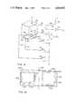
- FIG. 1is a cross sectional view of a digitizer pad having four terminals on a base ply in accordance with the invention.
- FIG. 2is a top view of the digitizer pad illustrated in FIG. 1 through section 2--2.
- FIG. 3is a cross-sectional view of a digitizer pad incorporating two facing pressure sensitive semiconducting layers in accordance with the invention.
- FIG. 4is a cross sectional view of a digitizer pad wherein the pressure sensitive semiconducting layer is disposed to cover the conductor on the top ply.
- FIG. 5is a top view of a digitizer pad in accordance with one embodiment of the invention where the resistor ply has a greater resistive gradient adjacent the terminals and a smaller resistive gradient across the center region.
- FIG. 6is a top view of one embodiment of a digitizer pad in accordance with the invention, having a variable resistance gradient across its surface in one of its spatial dimensions.
- FIG. 7is a top view of another embodiment of the digitizer pad in accordance with the invention comprising multiple pairs of terminals in a circular configuration.
- FIG. 8is another embodiment of the digitizer pad in accordance with the invention, having opposing nonparallel terminals for altering the potential profile across the surface of the digitizer pad.
- FIG. 9is a digitizer pad, such as that illustrated in FIG. 1, interconnected to appropriate switching circuitry to illustrate the operation and means of sequentially sensing the spatial characteristic of the point of contact in the x and y dimensions and the pressure dimension at the point of contact.
- FIG. 10is a folded digitizer pad in accordance with the invention wherein terminals and resistor plys are provided on both the base and the top plies.
- FIGS. 11A, 11B and 11Cillustrate the operation of the digitizer pad embodiment illustrated in FIG. 10.
- FIGS. 12A and 12Billustrate an embodiment of the digitizer pad having three terminals in each set whereby the sensing area is divided into quadrants.
- FIG. 13illustrates an embodiment somewhat similar to the embodiment of FIG. 12 wherein the terminals are lead pairs to facilitate electrical isolation of the quadrants.
- FIGS. 14A and 14Bare top views of two base plys, each having three terminals, a resistor ply, and a series of interdigitizing conductors.
- the base plysare shown at an angle with each other to illustrate two different axes.
- FIG. 15is a cross-sectional view of a digitizer pad, which includes the plys of FIGS. 14A and 14B.
- a digitizer pad 20in accordance with the invention comprises a base ply 22 and a top ply 24. Disposed at selected spaced locations on the top surface 34 of the base ply 22 are conductive terminals 26, 28, 30 and 32. The terminals 26 and 28 are paired together and positioned on opposite sides of the base ply 22 in parallel relationship to one another. Similarly, the terminals 30 and 32 are likewise paired together and oriented parallel to one another on opposite edges of the base ply 22.
- a resistor ply 36is disposed on the top surface 34 of the base ply 22 so that the resistor ply 36 is in electrical contact with the terminals 26, 28, 30 and 32 and extends across the region of the top surface 34 interior to and bounded by the terminals 26, 28, 30 and 32.
- the resistor ply 36does not extend to cover corner regions 40, 42, 44 and 46 so that the conduction paths through the resistor ply 36 between the edges of adjacent terminals will be made longer thereby increasing the resistance along each such conduction path. Such increased resistance results in increased isolation between adjacent terminals.
- the digitizer pad 20includes the top ply 24 which has a surface 50 on which is disposed a conductive ply 52.
- a pressure sensitive, semiconductive ply 54is incorporated between the conductive ply 52 and the resistor ply 36.
- the conductive ply 52is in normally nonconducting relationship to the resistor ply 36. This may be accomplished in any of a number of ways.
- the conductive ply 52may be physically spaced from the resistor ply 36 as illustrated in FIG. 1 so that the top ply 24 will have to be displaced downwardly to force the conductive ply 52 into electrically conductive relationship with the resistor ply 36.
- the pressure sensitive ply 54is disposed in intimate, electrically conducting relationship on top of the resistor ply 36.
- an additional pressure sensitive ply 56is disposed to cover and is in intimate, electrically conducting relationship with the conductive ply 52.
- the pressure sensitive conductive ply 54 of FIG. 3is eliminated and the pressure sensitive ply 56 is applied to cover the surface of the conductive ply 52.
- a pressure sensitive plysuch the plys 54 or 56 or both 54 and 56 are disposed between the conductor ply 52 and the resistor ply 36, facing contact surfaces 60 and 62 (also shown in FIGS. 1 and 3) of the base ply 22 and the top ply 24, respectively, may be in touching relationship.
- a light touching of the contact surfaces 60 and 62 in such an embodimentwill result in virtually no conduction through the pressure sensitive ply resulting in a normally opened, that is, a normally non-conducting relationship between the conductive ply 52 and the terminals 26, 28, 30 and 32.
- a force Fis applied to the top ply 24
- the junction resistance across the junction between the surfaces 60 and 62will decrease, thereby allowing conduction to occur between the conductive ply 52 and one of the terminals 26, 30, 28 or 32.
- a complete description and explanation of the pressure sensitive plyis described in U.S. Pat. No. 4,315,238.
- the conductive ply 52may be made of silver, copper, aluminum, or any other suitable conductive material.
- the resistor plymay be formed from a composition including, for example, carbon particles or from carbon ruthenium or any other suitable material which exhibits a resistance gradient along a length of the resistor material.
- electrical isolation between adjacent terminalsmay be enhanced by providing a resistor ply with a varying resistance gradient across the resistor ply.
- the resistor ply 36may be configured to have greater resistance in the regions 80, 82, 84, 86 adjacent to terminals 26, 28, 30 and 32, respectively, with the central region 88 of the resistor ply having a lesser resistive gradient.
- Such a variable resistive gradientmay be provided in any of a number of different ways such as by varying the concentration of conductive particles in the various regions. Hence, in the regions 80, 82, 84 and 86, the concentration of conductive particles would be lessened to increase the resistive gradient whereas the concentration of conductive particles in the region 88 would be increased to lower the resistive gradient.k
- the resistor ply 36may have a varying or non-linear resistive gradient across its length and width.
- FIG. 6shows a resistor ply 36 which as a resistive gradient which increases from right to left. This may be accomplished by providing a resistive ply with an increasing concentration of conductive particles in a direction from left to right.
- the resistive gradient between terminals 26 and 28will be non-linear.
- the resistive gradient between terminals 30 and 32will be substantially constant.
- the resistor ply 36allows for the creation of an electrical potential profile across the surface of the resistor ply which can be varied in accordance with user requirements.
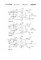
- a circular digitizer pad apparatus 100in accordance with the invention has three pairs of terminals, for example, terminal pair 102 and 104, terminal pair 106 and 108, and terminal pair 110 and 112.
- a resistor ply 114is provided in the central region bounded by the terminals where resistor ply 114 is configured to increase electrical isolation between adjacent terminals.
- a central, preferably grounded, terminal 116may be provided.
- the digitizer pad apparatus 100will comprise six terminal pairs where each terminal pair includes the terminal 116 and one of the terminals 102, 104, 106, 108, 110 or 112.
- another embodimentincludes a first pair of terminals comprising a terminal 120 and an opposite, spaced apart, parallel terminal 122 and a second pair of terminals comprising a first terminal 124 and a second terminal 126.
- the terminals 124 and 126are in a non-parallel orientation relative to each other. The voltage drop across the resistor ply between the two terminals 124 and 126 will therefore occur across a progressively shorter physical distance. This, of course, will affect the potential profile across the width and length of a resistor ply 128 between the terminals.
- the digitizer padidentifies both the spatial location and the magnitude of force applied at a point on the surface of the digitizer pad.
- a switching apparatus 160is provided whereby each terminal 26, 28, 30 and 32 is coupled via suitable lead 70, 72, 74 and 76, respectively (see FIG. 1 also), to selectively couple the terminals to an open switch contact, a grounded switch contact or a switch contact 6 to which a voltage from a voltage source is applied.
- the operation of the switchmay be sequential under either manual or computer control to determine the X-coordinate, Y-coordinate and then pressure (Z coordinate) of the point of contact 80 between the conductive ply 52 and the resistor ply 36.
- terminal 30 and 32are connected to the opened contact of switches 92 and 90, respectively.
- the lead 72is connected via switch 91 to the voltage source +V and the terminal 26 is connected via lead 70 and switch 93 to ground.
- a lead 78connected to the conductive ply 52, is coupled to an amplifier 79 so that the voltage at the output of the amplifier 79 will be the same as the voltage drop along the resistor ply 36 from the contact point 80 to the terminal 26.
- the point of contact 80moves closer to the terminal 26, the voltage will decrease and the output voltage from the amplifier 79 will decrease.
- a direct relationship between the voltage and the "X" coordinate locationexists and the "X" coordinate can therefore be determined from the value of the output voltage from amplifier 79.
- the Y-coordinate voltagemay be determined by interconnecting the terminal 32 to the voltage source +V via switch 90, interconnecting the terminal 30 to ground via switch 92, and coupling the terminals 26 and 28 to the opened contacts of switches 91 and 93, respectively.
- the voltage drop between the point of contact 80 and the terminal 32will be a measure of the distance Y from the terminal 30 to the contact point 80 as described in conjunction with the measurement of the coordinate X.
- the pressurecan be determined if a pressure sensitive ply 54 is disposed between the conductive ply 52 and the resistor ply 36 by coupling the terminals 26, 28, 30 and 32 to ground via switches 90, 91, 92 and 93 while simultaneously using switch 94 to connect the conductive ply 52 to a voltage source through resistor 161.
- switch 94to connect the conductive ply 52 to a voltage source through resistor 161.
- FIG. 10another embodiment of the present invention is illustrated whereby one pair of terminals 202 and 204 are disposed in spaced relationship to one another on a base ply 200 and a second pair of terminals 206 and 208 are disposed in spaced relationship on a top ply 210.
- the base ply 200 and the top ply 210may be a single ply with a fold 212 in the center whereby the top and base plys are folded into facing relationship to each other.
- the base ply 200 and the top ply 210may be entirely separate.
- a resistor ply 214Disposed between the terminals 202 and 204 is a resistor ply 214 on top of which is disposed a pressure sensitive ply 216 such as the particulated molybdenum disulfide material described in U.S. Pat. No. 4,315,238.
- the top ply 210has disposed thereon, between the terminals 206 and 208, a resistor ply 218 on top of which may be disposed a pressure sensitive semiconductor ply 220.
- the terminals 206 and 208will not come in contact with the terminals 202 and 204.
- FIGS. 11A, 11B and 11CThe operation of the embodiment of FIG. 10 is illustrated in FIGS. 11A, 11B and 11C.
- the terminal 202is connected to ground via switch 230 and the terminal 204 is connected to the voltage source +V via switch 230 to provide a voltage drop across the resistor ply between terminals 202 and 204.
- terminals 206 and 208are each coupled via switch 232 and 236 to the input of an amplifier 238.
- the voltage at the point of contact between the base ply 200 and the top ply 210will be applied to the input of the amplifier 238 and hence the output of the amplifier 238.
- the terminals 202 and 204are connected via switch 230 to the input of the amplifier 238 while the terminal 206 is connected to ground via switch 232.
- the Y-coordinate voltage at point 240which is the point on the surface of the digitizer pad at which the force F is applied, will appear at the output of the amplifier 238.
- the measure of pressuremay be obtained by connecting terminals 202 and 204 to voltage source +V via appropriate switching of switches 230 and 234 while simultaneously connecting the terminals 206 and 208 to ground via appropriate switching of switches 232 and 236.
- the voltage drop between the top ply 210 and the bottom ply 200will then be the voltage drop across the junction between the base ply 200 and the top ply 210 with the resistance varying, and hence the potential drop across the junction varying, as the pressure varies.
- another digitizer pad 300is illustrated including a base ply 302 on which is disposed three terminals 304, 306 and 308 in space apart, preferably parallel relationship. Disposed across a surface 310 of the base ply 302 on which the terminals 304, 306 and 308 are affixed is a resistor ply 312.
- the resistor plymay be of any configuration and may have any desired resistive gradient profile. In any event, the resistor ply 312 is applied to cover each of the terminals 304, 306 and 308 so as to be in electrical conducting relationship with those terminals.
- Digitizer pad 300also includes a top ply 314 which, like the base ply 302, includes three terminals 3-6, 318 and 320 which are in parallel orientation relative to one another and are spaced apart from one another.
- insulator pads 322are positioned at selected locations along each of the terminals 316, 318 and 320. The insulator pads 322 are positioned so that when the top ply 314 is folded over onto the base ply 302, the pads 322 will be between the crossover points between the terminals 316, 318 and 320 and the terminals 304, 306 and 308.
- the terminals 304, 306 and 308are orthogonally oriented with respect to the terminals on the top ply at the terminals 316, 318 and 320 on the top ply 314.
- a pressure sensitive semiconductive ply 324is disposed over the surface of the top ply 314 covering the terminals 316, 318 and 320 so that the semiconductor ply 324 will be located immediately adjacent to but in normally nonconducting relationship to the resistor ply 312.
- a switching network 326has leads X1, X2 and X3 which are coupled respectively to terminals 304, 306 and 308 and leads Y1, Y2 and Y3, respectively coupled to leads 316, 318 and 320.
- the switching network 326provides a means of applying the voltage from voltage source 328 across a selected two terminals from the set of three terminals on the base ply 302 or a select pair of terminals from the set of three terminals on the top ply 314.
- thee voltage from voltage source 328may be applied to the terminal 306 through lead X2 with terminal 304 coupled to ground.
- lead 316 and 318will be coupled by the switching network 326 to the output.
- the output voltagewill be a measure of the X dimension spatial coordinate in quadrant I.
- the Y-coordinate in quadrant Ican likewise be determined.
- the switching network 326can be configured to sequentially monitor quadrants I, II, III and IV in the X, Y and pressure (Z) coordinates to identify any point of force application. Once a particular point of force application is identified, the switching network 326 can eliminate scanning of all four quadrants and can remain in the quadrant of force application, continually sequencing through and determining the X, Y and pressure (Z) coordinates. By recording the parameters in the coordinates for a period of time, a profile of a change in the location of the application of force can be stored for later use in verifying future profiles.
- FIG. 13an embodiment of a digitizer pad 400 is illustrated having a configuration somewhat similar to that disclosed in FIGS. 12A and 12B.
- each terminalconsists of a pair of leads.
- terminal 404(corresponding to terminal 304) consists of a pair of leads W7 and W8.
- terminal 406consists of a pair of leads W9 an W10.
- leads W7 and W10are also coupled to ground.
- leads W1 and W4will be coupled to ground when a voltage is applied across leads W2 and W3.
- leads W9 and W12, W6 and W3will be coupled to ground while leads W10 and W11 and leads W4 and W5 are alternately coupled across the voltage source 428 and ground to sequentially determine a voltage constituting a measure of the X and Y coordinates of the point of force application in quadrant IV.
- the coupling of the leads W9, W12 and W6 and W3 to groundsurrounds the fourth quadrant with grounded leads thereby isolating quadrant IV.
- a digitizer padcapable of measuring position and pressure along three axes.
- the digitizer padcomprises a sandwich arrangement having two conductor plys respectively defining the X-axis and Y-axis with an insulative substrate between having a pressure sensitive semiconductive ply disposed on each side which is used in measuring the "Z-axis" or pressure parameter.
- a base ply 500has thereon three terminals 512, 514 and 516, a resistor ply 502, and a plurality of conductors 504 extending from resistor ply 501 and a plurality of second conductors 505, interleaved between but spaced from conductors 504. Terminals 512 and 514 are coupled across resistor ply 502.
- a base ply 506has thereon three terminals 518, 520 and 522, resistor ply 508, and a plurality of third conductors 510, extending from the resistor ply 508 and a plurality of fourth conductors 511 interleaved between but spaced from conductors 510. Terminals 518 and 520 are coupled across resistor ply 508.
- a nonconductive ply 528has disposed thereon a first pressure sensitive semiconductive layer 524 and a second pressure sensitive semiconductive layer 526.
- the pressure sensitive semiconductive layer 524generally corresponds to the area covered by conductors 504 and 505.
- the pressure sensitive semiconductive layer 526generally corresponds to the area covered by conductors 510 and 511.
- This nonconductive ply 528is then sandwiched between base plys 500 and 506 with conductors 504 and 505 correspondingly placed adjacent to pressure sensitive semiconductive layer 524 and conductors 510 and 511 being adjacent to pressure sensitive semiconductive layer 526.
- Ply 530represents the aggregate conductors and terminals 502, 504, 505, 512, 514, and 516.
- Ply 532represents the aggregate conductors and terminals 508, 510, 511, 518, 520 and 522.
- a force Fis applied to the digital pad illustrated in FIG. 15 and is registered via use of a switching means interconnected to the terminals and to a voltage source for selectively providing a voltage differential singly across selected pairs of terminals.
- a voltagemay be applied across terminal 512 and 514 (or 518 and 520) with the voltage at terminal 516 being proportional to the spatial location along the axis defined between terminal 512 and 514 (518 and 520) at which pressure is applied.
- the amount of pressure (a "Z" axis parameter) appliedis measured by setting the voltage at terminals 512 and 514 (518 and 520) at the same value (connecting the two terminals together) and applying a voltage across the terminals 512 and 516 (or 514 and 516) and then measuring the voltage drop across those terminals when pressure is applied.
- AC voltageseither in-phase or out-of-phase
- DC voltageseither in-phase or out-of-phase
Landscapes
- Engineering & Computer Science (AREA)
- General Engineering & Computer Science (AREA)
- Theoretical Computer Science (AREA)
- Human Computer Interaction (AREA)
- Physics & Mathematics (AREA)
- General Physics & Mathematics (AREA)
- Measurement Of Length, Angles, Or The Like Using Electric Or Magnetic Means (AREA)
Abstract
Description
Claims (2)
Priority Applications (1)
| Application Number | Priority Date | Filing Date | Title |
|---|---|---|---|
| US07/183,118US4810992A (en) | 1986-01-17 | 1988-04-19 | Digitizer pad |
Applications Claiming Priority (2)
| Application Number | Priority Date | Filing Date | Title |
|---|---|---|---|
| US06/820,757US4739299A (en) | 1986-01-17 | 1986-01-17 | Digitizer pad |
| US07/183,118US4810992A (en) | 1986-01-17 | 1988-04-19 | Digitizer pad |
Related Parent Applications (1)
| Application Number | Title | Priority Date | Filing Date |
|---|---|---|---|
| US06/820,757Continuation-In-PartUS4739299A (en) | 1986-01-17 | 1986-01-17 | Digitizer pad |
Publications (1)
| Publication Number | Publication Date |
|---|---|
| US4810992Atrue US4810992A (en) | 1989-03-07 |
Family
ID=26878772
Family Applications (1)
| Application Number | Title | Priority Date | Filing Date |
|---|---|---|---|
| US07/183,118Expired - LifetimeUS4810992A (en) | 1986-01-17 | 1988-04-19 | Digitizer pad |
Country Status (1)
| Country | Link |
|---|---|
| US (1) | US4810992A (en) |
Cited By (130)
| Publication number | Priority date | Publication date | Assignee | Title |
|---|---|---|---|---|
| US5008497A (en)* | 1990-03-22 | 1991-04-16 | Asher David J | Touch controller |
| US5159159A (en)* | 1990-12-07 | 1992-10-27 | Asher David J | Touch sensor and controller |
| US5184120A (en)* | 1991-04-04 | 1993-02-02 | Motorola, Inc. | Menu selection using adaptive force sensing resistor |
| US5192826A (en)* | 1990-01-09 | 1993-03-09 | Yamaha Corporation | Electronic musical instrument having an effect manipulator |
| US5243317A (en)* | 1991-12-11 | 1993-09-07 | Industrial Technology Research Institute | Magneto-resistor digitizer |
| US5266737A (en)* | 1990-01-10 | 1993-11-30 | Yamaha Corporation | Positional and pressure-sensitive apparatus for manually controlling musical tone of electronic musical instrument |
| US5272276A (en)* | 1990-01-16 | 1993-12-21 | Yamaha Corporation | Electronic musical instrument adapted to simulate a rubbed string instrument |
| US5278557A (en)* | 1991-02-19 | 1994-01-11 | Key Tronic Corporation | Cursor movement control key and electronic computer keyboard for computers having a video display |
| DE4221300A1 (en)* | 1992-06-29 | 1994-01-13 | Siemens Audiologische Technik | Data entry for a hearing aid |
| US5341433A (en)* | 1991-12-17 | 1994-08-23 | Siemens Aktiengesellschaft | Hearing aid device |
| US5431064A (en)* | 1992-09-18 | 1995-07-11 | Home Row, Inc. | Transducer array |
| GB2288665A (en)* | 1994-04-21 | 1995-10-25 | Samsung Display Devices Co Ltd | Information input apparatus having functions of both touch panel and digitizer, and driving method therof |
| US5502274A (en)* | 1989-01-03 | 1996-03-26 | The Hotz Corporation | Electronic musical instrument for playing along with prerecorded music and method of operation |
| US5532753A (en)* | 1993-03-22 | 1996-07-02 | Sony Deutschland Gmbh | Remote-controlled on-screen audio/video receiver control apparatus |
| US5550339A (en)* | 1994-10-31 | 1996-08-27 | Cts Corporation | Variable speed tactile switch |
| US5565657A (en)* | 1993-11-01 | 1996-10-15 | Xerox Corporation | Multidimensional user interface input device |
| US5573626A (en)* | 1993-05-26 | 1996-11-12 | Minnesota Mining And Manufacturing Company | Tape supply and applicator system including a tape splicing mechanism |
| US5581052A (en)* | 1993-10-18 | 1996-12-03 | Summagraphics Corporation | Pressure sensitive stylus having resiliently compressible tip element |
| US5583476A (en)* | 1990-07-13 | 1996-12-10 | Sensitron, Inc. | Flexible potentiometer |
| US5634476A (en)* | 1992-03-17 | 1997-06-03 | Fredric I. Orkin | Uterine contraction sensing device and method for manufacture and use thereof |
| US5656988A (en)* | 1995-07-24 | 1997-08-12 | Breed Technologies, Inc. | Force sensors with segmental electrodes |
| US5695473A (en)* | 1994-07-27 | 1997-12-09 | Sims Deltec, Inc. | Occlusion detection system for an infusion pump |
| US5711672A (en)* | 1994-07-01 | 1998-01-27 | Tv Interactive Data Corporation | Method for automatically starting execution and ending execution of a process in a host device based on insertion and removal of a storage media into the host device |
| WO1998014345A2 (en) | 1996-10-03 | 1998-04-09 | I.E.E. International Electronics & Engineering S.A.R.L. | Method and device for determining several parameters of a seated person |
| US5749735A (en)* | 1994-07-01 | 1998-05-12 | Tv Interactive Data Corporation | Interactive book, magazine and audio/video compact disk box |
| US5757304A (en)* | 1996-09-13 | 1998-05-26 | Tv Interactive Data Corporation | Remote control including an integrated circuit die supported by a printed publication and method for forming the remote control |
| US5789827A (en)* | 1993-05-10 | 1998-08-04 | Sensitron, Inc. | Two-wire interface to automobile horn relay circuit |
| US5864083A (en)* | 1997-12-18 | 1999-01-26 | Caren; Michael P. | Musical effect controller and system for an electric guitar |
| US5905485A (en)* | 1997-02-13 | 1999-05-18 | Breed Automotive Technology, Inc. | Controller with tactile sensors and method of fabricating same |
| US5935099A (en) | 1992-09-09 | 1999-08-10 | Sims Deltec, Inc. | Drug pump systems and methods |
| US5943044A (en)* | 1996-08-05 | 1999-08-24 | Interlink Electronics | Force sensing semiconductive touchpad |
| US5949354A (en)* | 1997-05-10 | 1999-09-07 | Acer Peripherals, Inc. | Computer pointing device |
| US6005181A (en)* | 1998-04-07 | 1999-12-21 | Interval Research Corporation | Electronic musical instrument |
| US6015163A (en)* | 1996-10-09 | 2000-01-18 | Langford; Gordon B. | System for measuring parameters related to automobile seat |
| US6131047A (en)* | 1997-12-30 | 2000-10-10 | Ericsson Inc. | Radiotelephones having contact-sensitive user interfaces and methods of operating same |
| EP0989509A3 (en)* | 1998-09-26 | 2001-03-21 | Electrotextiles Company Limited | Position detector constructed from fabric |
| US6223606B1 (en) | 1997-01-08 | 2001-05-01 | Trustees Of Boston University | Center of weight sensor |
| US6236301B1 (en) | 1996-09-04 | 2001-05-22 | Sensitron, Inc. | Cantilevered deflection sensing system |
| WO2001045032A1 (en)* | 1999-12-14 | 2001-06-21 | Moore Corporation Limited | Radio frequency identification tagging, encoding/reading through a digitizer tablet |
| US6360597B1 (en) | 1997-01-08 | 2002-03-26 | The Trustees Of Boston University | In-shoe remote telemetry gait analysis system |
| US6392527B1 (en) | 1996-09-04 | 2002-05-21 | Sensitron, Inc. | Impact detection system |
| US20020183693A1 (en)* | 1992-09-09 | 2002-12-05 | Sims Deltec, Inc. | Drug pump systems and methods |
| US6546813B2 (en) | 1997-01-08 | 2003-04-15 | The Trustees Of Boston University | Patient monitoring system employing array of force sensors on a bedsheet or similar substrate |
| US20030076301A1 (en)* | 2001-10-22 | 2003-04-24 | Apple Computer, Inc. | Method and apparatus for accelerated scrolling |
| US20030163789A1 (en)* | 2002-02-28 | 2003-08-28 | Blomquist Michael L. | Programmable medical infusion pump displaying a banner |
| US6650867B2 (en) | 1997-03-14 | 2003-11-18 | Smartpaper Networks Corporation | Remote control apparatus and method of transmitting data to a host device |
| US6703552B2 (en) | 2001-07-19 | 2004-03-09 | Lippold Haken | Continuous music keyboard |
| US20040130528A1 (en)* | 2003-01-07 | 2004-07-08 | Baker Jeffrey R. | Miniature highly manufacturable mouse pointing device |
| EP1469378A1 (en)* | 2003-04-16 | 2004-10-20 | IEE INTERNATIONAL ELECTRONICS & ENGINEERING S.A. | Position detection apparatus |
| EP1487114A1 (en)* | 2003-05-28 | 2004-12-15 | Freescale Semiconductor, Inc. | Keypad signal input apparatus |
| US20050052425A1 (en)* | 2003-08-18 | 2005-03-10 | Zadesky Stephen Paul | Movable touch pad with added functionality |
| US20050110768A1 (en)* | 2003-11-25 | 2005-05-26 | Greg Marriott | Touch pad for handheld device |
| US6909354B2 (en) | 2001-02-08 | 2005-06-21 | Interlink Electronics, Inc. | Electronic pressure sensitive transducer apparatus and method for manufacturing same |
| WO2006002661A1 (en)* | 2004-06-30 | 2006-01-12 | Freescale Semiconductor, Inc. | Keypad signal input apparatus |
| US20060007172A1 (en)* | 2004-06-23 | 2006-01-12 | Interlink Electronics, Inc. | Force sensing resistor with calibration element and method of manufacturing same |
| US20060020418A1 (en)* | 2004-05-14 | 2006-01-26 | Moore Robert H | Nip press sensing system including a sensor strip having sensor interface electronics associated therewith and methods of operating the same |
| US20060032680A1 (en)* | 2004-08-16 | 2006-02-16 | Fingerworks, Inc. | Method of increasing the spatial resolution of touch sensitive devices |
| US20060158433A1 (en)* | 2002-11-25 | 2006-07-20 | Iee International Electronics & Engineering S.A. | Data input device |
| US20060181517A1 (en)* | 2005-02-11 | 2006-08-17 | Apple Computer, Inc. | Display actuator |
| EP1462925A3 (en)* | 2003-03-11 | 2006-10-25 | Eastman Kodak Company | Resistive touch screen with variable resistivity layer |
| US20070013671A1 (en)* | 2001-10-22 | 2007-01-18 | Apple Computer, Inc. | Touch pad for handheld device |
| WO2007016876A1 (en)* | 2005-08-11 | 2007-02-15 | Yuancai Wu | An information inputting device |
| US20070052044A1 (en)* | 2005-09-06 | 2007-03-08 | Larry Forsblad | Scrolling input arrangements using capacitive sensors on a flexible membrane |
| US20070083822A1 (en)* | 2001-10-22 | 2007-04-12 | Apple Computer, Inc. | Method and apparatus for use of rotational user inputs |
| US20070080952A1 (en)* | 2005-10-11 | 2007-04-12 | Brian Lynch | Center button isolation ring |
| US20070085841A1 (en)* | 2001-10-22 | 2007-04-19 | Apple Computer, Inc. | Method and apparatus for accelerated scrolling |
| US20070084331A1 (en)* | 2005-10-15 | 2007-04-19 | Lippold Haken | Position correction for an electronic musical instrument |
| US20070146349A1 (en)* | 2005-12-27 | 2007-06-28 | Interlink Electronics, Inc. | Touch input device having interleaved scroll sensors |
| US20070152977A1 (en)* | 2005-12-30 | 2007-07-05 | Apple Computer, Inc. | Illuminated touchpad |
| US20070152983A1 (en)* | 2005-12-30 | 2007-07-05 | Apple Computer, Inc. | Touch pad with symbols based on mode |
| US20070242057A1 (en)* | 2002-02-25 | 2007-10-18 | Apple Inc. | Touch pad for handheld device |
| US20080006453A1 (en)* | 2006-07-06 | 2008-01-10 | Apple Computer, Inc., A California Corporation | Mutual capacitance touch sensing device |
| US20080007533A1 (en)* | 2006-07-06 | 2008-01-10 | Apple Computer, Inc., A California Corporation | Capacitance sensing electrode with integrated I/O mechanism |
| US20080006454A1 (en)* | 2006-07-10 | 2008-01-10 | Apple Computer, Inc. | Mutual capacitance touch sensing device |
| US20080018616A1 (en)* | 2003-11-25 | 2008-01-24 | Apple Computer, Inc. | Techniques for interactive input to portable electronic devices |
| US20080018609A1 (en)* | 2006-07-20 | 2008-01-24 | Interlink Electronics, Inc. | Shape adaptable resistive touchpad |
| US20080088600A1 (en)* | 2006-10-11 | 2008-04-17 | Apple Inc. | Method and apparatus for implementing multiple push buttons in a user input device |
| US20080087476A1 (en)* | 2006-10-11 | 2008-04-17 | Apple Inc. | Sensor configurations in a user input device |
| US20080088596A1 (en)* | 2006-10-11 | 2008-04-17 | Apple Inc. | Gimballed scroll wheel |
| US20080111795A1 (en)* | 2006-11-13 | 2008-05-15 | Apple Inc. | Method of capacitively sensing finger position |
| WO2008080812A1 (en) | 2006-12-21 | 2008-07-10 | Dav | Electric control module, particularly for motor vehicles |
| US20080314165A1 (en)* | 2005-06-16 | 2008-12-25 | Rosenberg Ilya D | Method for Manufacturing Long Force Sensors Using Screen Printing Technology |
| US20090020343A1 (en)* | 2007-07-17 | 2009-01-22 | Apple Inc. | Resistive force sensor with capacitive discrimination |
| US20090050376A1 (en)* | 2007-08-21 | 2009-02-26 | Jin Jeon | Method of detecting a touch position and touch panel for performing the same |
| US20090058687A1 (en)* | 2007-09-04 | 2009-03-05 | Apple Inc. | Compact input device |
| US20090064031A1 (en)* | 2007-09-04 | 2009-03-05 | Apple Inc. | Scrolling techniques for user interfaces |
| EP2037473A1 (en) | 2007-09-17 | 2009-03-18 | Dav | Electric switch with tactile surface |
| US20090073130A1 (en)* | 2007-09-17 | 2009-03-19 | Apple Inc. | Device having cover with integrally formed sensor |
| WO2009047235A2 (en) | 2007-10-08 | 2009-04-16 | Dav | Method for controlling a touch surface control device and electric touch surface control device including means for implementing said method |
| US20090141046A1 (en)* | 2007-12-03 | 2009-06-04 | Apple Inc. | Multi-dimensional scroll wheel |
| WO2009083493A1 (en) | 2007-12-20 | 2009-07-09 | Dav | Method of controlling a touch-surface control device and corresponding control device |
| US20090179854A1 (en)* | 2008-01-11 | 2009-07-16 | Apple Inc. | Dynamic input graphic display |
| US20090197059A1 (en)* | 2008-02-01 | 2009-08-06 | Apple Inc. | Co-extruded materials and methods |
| US20090273573A1 (en)* | 2006-07-06 | 2009-11-05 | Apple Inc. | Mutual capacitance touch sensing device |
| US20100020028A1 (en)* | 2006-08-23 | 2010-01-28 | Patrice Laurent | Control Module, In Particular For An Automotive Vehicle |
| US20100058251A1 (en)* | 2008-08-27 | 2010-03-04 | Apple Inc. | Omnidirectional gesture detection |
| US20100149127A1 (en)* | 2008-12-17 | 2010-06-17 | Apple Inc. | Integrated contact switch and touch sensor elements |
| US20100182167A1 (en)* | 2007-06-25 | 2010-07-22 | Dav | Electric control device |
| US20100201503A1 (en)* | 2007-06-01 | 2010-08-12 | Dav | Haptic feedback tactile control device |
| US7795553B2 (en) | 2006-09-11 | 2010-09-14 | Apple Inc. | Hybrid button |
| US20100289759A1 (en)* | 2009-05-15 | 2010-11-18 | Apple Inc. | Input device with optimized capacitive sensing |
| US20100288568A1 (en)* | 2007-07-31 | 2010-11-18 | Dav | Pressure sensitive touch-surface control device |
| US20110000773A1 (en)* | 2007-03-02 | 2011-01-06 | Dav | Electric control device for an automobile |
| US20110007022A1 (en)* | 2007-03-02 | 2011-01-13 | Dav | Touch surface sensor |
| US20110005845A1 (en)* | 2009-07-07 | 2011-01-13 | Apple Inc. | Touch sensing device having conductive nodes |
| US20110025618A1 (en)* | 2007-12-20 | 2011-02-03 | Dav | Method for detecting an angular variation of a control path on a touch surface and corresponding control module |
| USRE42738E1 (en) | 1997-10-28 | 2011-09-27 | Apple Inc. | Portable computers |
| US8133197B2 (en) | 2008-05-02 | 2012-03-13 | Smiths Medical Asd, Inc. | Display for pump |
| US8149131B2 (en) | 2006-08-03 | 2012-04-03 | Smiths Medical Asd, Inc. | Interface for medical infusion pump |
| WO2012085363A1 (en) | 2010-12-22 | 2012-06-28 | Valeo Systemes Thermiques | Multifunction control button and device |
| WO2012085360A1 (en) | 2010-12-21 | 2012-06-28 | Valeo Systemes Thermiques | Motor vehicle control device |
| US8435206B2 (en) | 2006-08-03 | 2013-05-07 | Smiths Medical Asd, Inc. | Interface for medical infusion pump |
| US8504179B2 (en) | 2002-02-28 | 2013-08-06 | Smiths Medical Asd, Inc. | Programmable medical infusion pump |
| US8587422B2 (en) | 2010-03-31 | 2013-11-19 | Tk Holdings, Inc. | Occupant sensing system |
| US8607651B2 (en) | 2011-09-30 | 2013-12-17 | Sensitronics, LLC | Hybrid capacitive force sensors |
| US8725230B2 (en) | 2010-04-02 | 2014-05-13 | Tk Holdings Inc. | Steering wheel with hand sensors |
| US8816967B2 (en) | 2008-09-25 | 2014-08-26 | Apple Inc. | Capacitive sensor having electrodes arranged on the substrate and the flex circuit |
| US8858526B2 (en) | 2006-08-03 | 2014-10-14 | Smiths Medical Asd, Inc. | Interface for medical infusion pump |
| US8954336B2 (en) | 2004-02-23 | 2015-02-10 | Smiths Medical Asd, Inc. | Server for medical device |
| US8965707B2 (en) | 2006-08-03 | 2015-02-24 | Smiths Medical Asd, Inc. | Interface for medical infusion pump |
| US8983732B2 (en) | 2010-04-02 | 2015-03-17 | Tk Holdings Inc. | Steering wheel with hand pressure sensing |
| US9007190B2 (en) | 2010-03-31 | 2015-04-14 | Tk Holdings Inc. | Steering wheel sensors |
| US9111516B1 (en)* | 2014-06-08 | 2015-08-18 | Remo Saraceni | Portable floor piano with folding keyboard |
| US9214146B2 (en)* | 2013-03-15 | 2015-12-15 | Sensitronics, LLC | Electronic musical instruments using mouthpieces and FSR sensors |
| US20160124559A1 (en)* | 2014-11-05 | 2016-05-05 | Roger Linn | Polyphonic Multi-Dimensional Controller with Sensor Having Force-Sensing Potentiometers |
| US9454256B2 (en) | 2008-03-14 | 2016-09-27 | Apple Inc. | Sensor configurations of an input device that are switchable based on mode |
| US9696223B2 (en) | 2012-09-17 | 2017-07-04 | Tk Holdings Inc. | Single layer force sensor |
| US9727031B2 (en) | 2012-04-13 | 2017-08-08 | Tk Holdings Inc. | Pressure sensor including a pressure sensitive material for use with control systems and methods of using the same |
| US20190073076A1 (en)* | 2017-09-07 | 2019-03-07 | Acer Incorporated | Pressure Sensor and Pressure Sensing Method |
| US10682460B2 (en) | 2013-01-28 | 2020-06-16 | Smiths Medical Asd, Inc. | Medication safety devices and methods |
Citations (5)
| Publication number | Priority date | Publication date | Assignee | Title |
|---|---|---|---|---|
| US4315238A (en)* | 1979-09-24 | 1982-02-09 | Eventoff Franklin Neal | Bounceless switch apparatus |
| US4319078A (en)* | 1979-04-02 | 1982-03-09 | Nippon Telegraph & Telephone Public Corporation | Apparatus for detecting X and Y coordinates of input points |
| US4441097A (en)* | 1979-01-29 | 1984-04-03 | Antroy Enterprises, Inc. | Device for controlling a circuit |
| US4484026A (en)* | 1983-03-15 | 1984-11-20 | Koala Technologies Corporation | Touch tablet data device |
| US4570149A (en)* | 1983-03-15 | 1986-02-11 | Koala Technologies Corporation | Simplified touch tablet data device |
- 1988
- 1988-04-19USUS07/183,118patent/US4810992A/ennot_activeExpired - Lifetime
Patent Citations (5)
| Publication number | Priority date | Publication date | Assignee | Title |
|---|---|---|---|---|
| US4441097A (en)* | 1979-01-29 | 1984-04-03 | Antroy Enterprises, Inc. | Device for controlling a circuit |
| US4319078A (en)* | 1979-04-02 | 1982-03-09 | Nippon Telegraph & Telephone Public Corporation | Apparatus for detecting X and Y coordinates of input points |
| US4315238A (en)* | 1979-09-24 | 1982-02-09 | Eventoff Franklin Neal | Bounceless switch apparatus |
| US4484026A (en)* | 1983-03-15 | 1984-11-20 | Koala Technologies Corporation | Touch tablet data device |
| US4570149A (en)* | 1983-03-15 | 1986-02-11 | Koala Technologies Corporation | Simplified touch tablet data device |
Cited By (268)
| Publication number | Priority date | Publication date | Assignee | Title |
|---|---|---|---|---|
| US5502274A (en)* | 1989-01-03 | 1996-03-26 | The Hotz Corporation | Electronic musical instrument for playing along with prerecorded music and method of operation |
| US5619003A (en)* | 1989-01-03 | 1997-04-08 | The Hotz Corporation | Electronic musical instrument dynamically responding to varying chord and scale input information |
| US5192826A (en)* | 1990-01-09 | 1993-03-09 | Yamaha Corporation | Electronic musical instrument having an effect manipulator |
| US5266737A (en)* | 1990-01-10 | 1993-11-30 | Yamaha Corporation | Positional and pressure-sensitive apparatus for manually controlling musical tone of electronic musical instrument |
| US5272276A (en)* | 1990-01-16 | 1993-12-21 | Yamaha Corporation | Electronic musical instrument adapted to simulate a rubbed string instrument |
| US5008497A (en)* | 1990-03-22 | 1991-04-16 | Asher David J | Touch controller |
| US5583476A (en)* | 1990-07-13 | 1996-12-10 | Sensitron, Inc. | Flexible potentiometer |
| US5159159A (en)* | 1990-12-07 | 1992-10-27 | Asher David J | Touch sensor and controller |
| US5278557A (en)* | 1991-02-19 | 1994-01-11 | Key Tronic Corporation | Cursor movement control key and electronic computer keyboard for computers having a video display |
| US5184120A (en)* | 1991-04-04 | 1993-02-02 | Motorola, Inc. | Menu selection using adaptive force sensing resistor |
| US5243317A (en)* | 1991-12-11 | 1993-09-07 | Industrial Technology Research Institute | Magneto-resistor digitizer |
| US5341433A (en)* | 1991-12-17 | 1994-08-23 | Siemens Aktiengesellschaft | Hearing aid device |
| US5634476A (en)* | 1992-03-17 | 1997-06-03 | Fredric I. Orkin | Uterine contraction sensing device and method for manufacture and use thereof |
| DE4221300A1 (en)* | 1992-06-29 | 1994-01-13 | Siemens Audiologische Technik | Data entry for a hearing aid |
| US5935099A (en) | 1992-09-09 | 1999-08-10 | Sims Deltec, Inc. | Drug pump systems and methods |
| US7347836B2 (en) | 1992-09-09 | 2008-03-25 | Smiths Medical, Inc. | Drug pump systems and methods |
| US7654976B2 (en) | 1992-09-09 | 2010-02-02 | Smiths Medical Asd, Inc. | Drug pump systems and methods |
| US20020183693A1 (en)* | 1992-09-09 | 2002-12-05 | Sims Deltec, Inc. | Drug pump systems and methods |
| US5578765A (en)* | 1992-09-18 | 1996-11-26 | Incontrol Solutions, Inc. | Transducer array |
| US5583303A (en)* | 1992-09-18 | 1996-12-10 | Incontrol Solutions, Inc. | Transducer array |
| US5431064A (en)* | 1992-09-18 | 1995-07-11 | Home Row, Inc. | Transducer array |
| US5532753A (en)* | 1993-03-22 | 1996-07-02 | Sony Deutschland Gmbh | Remote-controlled on-screen audio/video receiver control apparatus |
| US5789827A (en)* | 1993-05-10 | 1998-08-04 | Sensitron, Inc. | Two-wire interface to automobile horn relay circuit |
| US5573626A (en)* | 1993-05-26 | 1996-11-12 | Minnesota Mining And Manufacturing Company | Tape supply and applicator system including a tape splicing mechanism |
| US5581052A (en)* | 1993-10-18 | 1996-12-03 | Summagraphics Corporation | Pressure sensitive stylus having resiliently compressible tip element |
| US5565657A (en)* | 1993-11-01 | 1996-10-15 | Xerox Corporation | Multidimensional user interface input device |
| GB2288665B (en)* | 1994-04-21 | 1998-05-13 | Samsung Display Devices Co Ltd | Information input apparatus having functions of both touch panel and digitizer,and driving method thereof |
| GB2288665A (en)* | 1994-04-21 | 1995-10-25 | Samsung Display Devices Co Ltd | Information input apparatus having functions of both touch panel and digitizer, and driving method therof |
| US5839905A (en)* | 1994-07-01 | 1998-11-24 | Tv Interactive Data Corporation | Remote control for indicating specific information to be displayed by a host device |
| US5957695A (en)* | 1994-07-01 | 1999-09-28 | Tv Interactive Corporation | Structure and method for displaying commercials and sending purchase orders by computer |
| US5788507A (en)* | 1994-07-01 | 1998-08-04 | Tv Interactive Data Corporation | Method for remotely controlling a display of information from a storage media |
| US5749735A (en)* | 1994-07-01 | 1998-05-12 | Tv Interactive Data Corporation | Interactive book, magazine and audio/video compact disk box |
| US5795156A (en)* | 1994-07-01 | 1998-08-18 | Tv Interactive Data Corporation | Host device equipped with means for starting a process in response to detecting insertion of a storage media |
| US6249863B1 (en) | 1994-07-01 | 2001-06-19 | Tv Interactive Data Corporation | Host device equipped with means for starting a process in response to detecting insertion of a storage media |
| US5911582A (en)* | 1994-07-01 | 1999-06-15 | Tv Interactive Data Corporation | Interactive system including a host device for displaying information remotely controlled by a remote control |
| US5711672A (en)* | 1994-07-01 | 1998-01-27 | Tv Interactive Data Corporation | Method for automatically starting execution and ending execution of a process in a host device based on insertion and removal of a storage media into the host device |
| US5695473A (en)* | 1994-07-27 | 1997-12-09 | Sims Deltec, Inc. | Occlusion detection system for an infusion pump |
| US5550339A (en)* | 1994-10-31 | 1996-08-27 | Cts Corporation | Variable speed tactile switch |
| US5656988A (en)* | 1995-07-24 | 1997-08-12 | Breed Technologies, Inc. | Force sensors with segmental electrodes |
| US6239790B1 (en) | 1996-08-05 | 2001-05-29 | Interlink Electronics | Force sensing semiconductive touchpad |
| US5943044A (en)* | 1996-08-05 | 1999-08-24 | Interlink Electronics | Force sensing semiconductive touchpad |
| US6236301B1 (en) | 1996-09-04 | 2001-05-22 | Sensitron, Inc. | Cantilevered deflection sensing system |
| US6392527B1 (en) | 1996-09-04 | 2002-05-21 | Sensitron, Inc. | Impact detection system |
| US5757304A (en)* | 1996-09-13 | 1998-05-26 | Tv Interactive Data Corporation | Remote control including an integrated circuit die supported by a printed publication and method for forming the remote control |
| US6348663B1 (en) | 1996-10-03 | 2002-02-19 | I.E.E. International Electronics & Engineering S.A.R.L. | Method and device for determining several parameters of a seated person |
| WO1998014345A3 (en)* | 1996-10-03 | 1998-06-04 | Iee Sarl | Method and device for determining several parameters of a seated person |
| WO1998014345A2 (en) | 1996-10-03 | 1998-04-09 | I.E.E. International Electronics & Engineering S.A.R.L. | Method and device for determining several parameters of a seated person |
| US6015163A (en)* | 1996-10-09 | 2000-01-18 | Langford; Gordon B. | System for measuring parameters related to automobile seat |
| US6223606B1 (en) | 1997-01-08 | 2001-05-01 | Trustees Of Boston University | Center of weight sensor |
| US6546813B2 (en) | 1997-01-08 | 2003-04-15 | The Trustees Of Boston University | Patient monitoring system employing array of force sensors on a bedsheet or similar substrate |
| US6840117B2 (en) | 1997-01-08 | 2005-01-11 | The Trustees Of Boston University | Patient monitoring system employing array of force sensors on a bedsheet or similar substrate |
| US6360597B1 (en) | 1997-01-08 | 2002-03-26 | The Trustees Of Boston University | In-shoe remote telemetry gait analysis system |
| US5905485A (en)* | 1997-02-13 | 1999-05-18 | Breed Automotive Technology, Inc. | Controller with tactile sensors and method of fabricating same |
| US6968151B2 (en) | 1997-03-14 | 2005-11-22 | Smartpaper Networks Corporation | Remote control |
| US6650867B2 (en) | 1997-03-14 | 2003-11-18 | Smartpaper Networks Corporation | Remote control apparatus and method of transmitting data to a host device |
| US20040086840A1 (en)* | 1997-03-14 | 2004-05-06 | Redford Peter M. | Method of detachably attaching an insert to a remote control base and the resulting remot control |
| US20050255435A1 (en)* | 1997-03-14 | 2005-11-17 | Redford Peter M | Insert for use with a remote control base |
| US5949354A (en)* | 1997-05-10 | 1999-09-07 | Acer Peripherals, Inc. | Computer pointing device |
| USRE45559E1 (en) | 1997-10-28 | 2015-06-09 | Apple Inc. | Portable computers |
| USRE46548E1 (en) | 1997-10-28 | 2017-09-12 | Apple Inc. | Portable computers |
| USRE42738E1 (en) | 1997-10-28 | 2011-09-27 | Apple Inc. | Portable computers |
| USRE44855E1 (en) | 1997-10-28 | 2014-04-22 | Apple Inc. | Multi-functional cellular telephone |
| USRE44103E1 (en) | 1997-10-28 | 2013-03-26 | Apple Inc. | Portable computers |
| US5864083A (en)* | 1997-12-18 | 1999-01-26 | Caren; Michael P. | Musical effect controller and system for an electric guitar |
| US8812059B2 (en) | 1997-12-30 | 2014-08-19 | Ericsson, Inc. | Radiotelephones having contact-sensitive user interfaces and methods of operating same |
| US6131047A (en)* | 1997-12-30 | 2000-10-10 | Ericsson Inc. | Radiotelephones having contact-sensitive user interfaces and methods of operating same |
| US6278888B1 (en) | 1997-12-30 | 2001-08-21 | Ericsson Inc. | Radiotelephones having contact-sensitive user interfaces and methods of operating same |
| USRE43931E1 (en) | 1997-12-30 | 2013-01-15 | Ericsson Inc. | Radiotelephones having contact-sensitive user interfaces and methods of operating same |
| US6005181A (en)* | 1998-04-07 | 1999-12-21 | Interval Research Corporation | Electronic musical instrument |
| EP1132854A1 (en)* | 1998-09-26 | 2001-09-12 | Electrotextiles Company Limited | Detector constructed from fabric |
| US6501465B2 (en) | 1998-09-26 | 2002-12-31 | Eleksen Limited | Detector constructed from fabric using measured current to determine pressure |
| EP0989509A3 (en)* | 1998-09-26 | 2001-03-21 | Electrotextiles Company Limited | Position detector constructed from fabric |
| EP1100044A1 (en)* | 1998-09-26 | 2001-05-16 | Electrotextiles Company Limited | Detector constructed from fabric |
| EP1132853A1 (en)* | 1998-09-26 | 2001-09-12 | Electrotextiles Company Limited | Detector constructed from fabric |
| US6369804B1 (en) | 1998-09-26 | 2002-04-09 | Eleksen Limited | Detector constructed from fabric having non-uniform conductivity |
| US6437258B1 (en) | 1998-09-26 | 2002-08-20 | Eleksen Limited | Detector constructed from fabric having planes with differing conductance |
| US6492980B2 (en) | 1998-09-26 | 2002-12-10 | Eleksen Limited | Multiplexing detector constructed from fabric |
| WO2001045032A1 (en)* | 1999-12-14 | 2001-06-21 | Moore Corporation Limited | Radio frequency identification tagging, encoding/reading through a digitizer tablet |
| AU783209B2 (en)* | 1999-12-14 | 2005-10-06 | Moore Corporation Limited | Radio frequency identification tagging, encoding/reading through a digitizer tablet |
| US20050156705A1 (en)* | 2001-02-08 | 2005-07-21 | Interlink Electronics, Inc. | Electronic pressure sensitive transducer apparatus and method for manufacturing same |
| US6909354B2 (en) | 2001-02-08 | 2005-06-21 | Interlink Electronics, Inc. | Electronic pressure sensitive transducer apparatus and method for manufacturing same |
| US7213323B2 (en) | 2001-02-08 | 2007-05-08 | Interlink Electronics, Inc. | Method of forming an electronic pressure sensitive transducer on a printed circuit board |
| US6703552B2 (en) | 2001-07-19 | 2004-03-09 | Lippold Haken | Continuous music keyboard |
| US20070083822A1 (en)* | 2001-10-22 | 2007-04-12 | Apple Computer, Inc. | Method and apparatus for use of rotational user inputs |
| US7345671B2 (en) | 2001-10-22 | 2008-03-18 | Apple Inc. | Method and apparatus for use of rotational user inputs |
| US20070290990A1 (en)* | 2001-10-22 | 2007-12-20 | Robbin Jeffrey L | Method and Apparatus for Use of Rotational User Inputs |
| US9977518B2 (en) | 2001-10-22 | 2018-05-22 | Apple Inc. | Scrolling based on rotational movement |
| US7710393B2 (en) | 2001-10-22 | 2010-05-04 | Apple Inc. | Method and apparatus for accelerated scrolling |
| US7710394B2 (en) | 2001-10-22 | 2010-05-04 | Apple Inc. | Method and apparatus for use of rotational user inputs |
| US7710409B2 (en) | 2001-10-22 | 2010-05-04 | Apple Inc. | Method and apparatus for use of rotational user inputs |
| US20030076301A1 (en)* | 2001-10-22 | 2003-04-24 | Apple Computer, Inc. | Method and apparatus for accelerated scrolling |
| US7312785B2 (en) | 2001-10-22 | 2007-12-25 | Apple Inc. | Method and apparatus for accelerated scrolling |
| US20070013671A1 (en)* | 2001-10-22 | 2007-01-18 | Apple Computer, Inc. | Touch pad for handheld device |
| US7348967B2 (en) | 2001-10-22 | 2008-03-25 | Apple Inc. | Touch pad for handheld device |
| US9009626B2 (en) | 2001-10-22 | 2015-04-14 | Apple Inc. | Method and apparatus for accelerated scrolling |
| US20070085841A1 (en)* | 2001-10-22 | 2007-04-19 | Apple Computer, Inc. | Method and apparatus for accelerated scrolling |
| US8952886B2 (en) | 2001-10-22 | 2015-02-10 | Apple Inc. | Method and apparatus for accelerated scrolling |
| US20070080936A1 (en)* | 2001-10-22 | 2007-04-12 | Apple Computer, Inc. | Method and apparatus for accelerated scrolling |
| US20080018615A1 (en)* | 2002-02-25 | 2008-01-24 | Apple Inc. | Touch pad for handheld device |
| US7333092B2 (en) | 2002-02-25 | 2008-02-19 | Apple Computer, Inc. | Touch pad for handheld device |
| US8446370B2 (en) | 2002-02-25 | 2013-05-21 | Apple Inc. | Touch pad for handheld device |
| US10353565B2 (en) | 2002-02-25 | 2019-07-16 | Apple Inc. | Input apparatus and button arrangement for handheld device |
| US20070242057A1 (en)* | 2002-02-25 | 2007-10-18 | Apple Inc. | Touch pad for handheld device |
| US20070276525A1 (en)* | 2002-02-25 | 2007-11-29 | Apple Inc. | Touch pad for handheld device |
| US8504179B2 (en) | 2002-02-28 | 2013-08-06 | Smiths Medical Asd, Inc. | Programmable medical infusion pump |
| US8250483B2 (en) | 2002-02-28 | 2012-08-21 | Smiths Medical Asd, Inc. | Programmable medical infusion pump displaying a banner |
| US20030163789A1 (en)* | 2002-02-28 | 2003-08-28 | Blomquist Michael L. | Programmable medical infusion pump displaying a banner |
| US20060158433A1 (en)* | 2002-11-25 | 2006-07-20 | Iee International Electronics & Engineering S.A. | Data input device |
| US7800586B2 (en)* | 2002-11-25 | 2010-09-21 | IEE International Elecronics & Engineering S.A. | Data input device |
| US7050045B2 (en) | 2003-01-07 | 2006-05-23 | Interlink Electronics, Inc. | Miniature highly manufacturable mouse pointing device |
| US20040130528A1 (en)* | 2003-01-07 | 2004-07-08 | Baker Jeffrey R. | Miniature highly manufacturable mouse pointing device |
| EP1462925A3 (en)* | 2003-03-11 | 2006-10-25 | Eastman Kodak Company | Resistive touch screen with variable resistivity layer |
| WO2004092940A3 (en)* | 2003-04-16 | 2005-03-03 | Iee Sarl | Position detection device |
| CN100381989C (en)* | 2003-04-16 | 2008-04-16 | Iee国际电子及工程股份有限公司 | Position detection device |
| US8184106B2 (en) | 2003-04-16 | 2012-05-22 | Iee International Electronics & Engineering S.A. | Position detection device |
| EP1469378A1 (en)* | 2003-04-16 | 2004-10-20 | IEE INTERNATIONAL ELECTRONICS & ENGINEERING S.A. | Position detection apparatus |
| EP1487114A1 (en)* | 2003-05-28 | 2004-12-15 | Freescale Semiconductor, Inc. | Keypad signal input apparatus |
| US20070052691A1 (en)* | 2003-08-18 | 2007-03-08 | Apple Computer, Inc. | Movable touch pad with added functionality |
| US7499040B2 (en) | 2003-08-18 | 2009-03-03 | Apple Inc. | Movable touch pad with added functionality |
| US20050052425A1 (en)* | 2003-08-18 | 2005-03-10 | Zadesky Stephen Paul | Movable touch pad with added functionality |
| US8749493B2 (en) | 2003-08-18 | 2014-06-10 | Apple Inc. | Movable touch pad with added functionality |
| US20060250377A1 (en)* | 2003-08-18 | 2006-11-09 | Apple Computer, Inc. | Actuating user interface for media player |
| US20070273671A1 (en)* | 2003-08-18 | 2007-11-29 | Zadesky Stephen P | Movable touch pad with added functionality |
| US8552990B2 (en) | 2003-11-25 | 2013-10-08 | Apple Inc. | Touch pad for handheld device |
| US20050110768A1 (en)* | 2003-11-25 | 2005-05-26 | Greg Marriott | Touch pad for handheld device |
| US7495659B2 (en) | 2003-11-25 | 2009-02-24 | Apple Inc. | Touch pad for handheld device |
| US8933890B2 (en) | 2003-11-25 | 2015-01-13 | Apple Inc. | Techniques for interactive input to portable electronic devices |
| US20080018616A1 (en)* | 2003-11-25 | 2008-01-24 | Apple Computer, Inc. | Techniques for interactive input to portable electronic devices |
| US20080012837A1 (en)* | 2003-11-25 | 2008-01-17 | Apple Computer, Inc. | Touch pad for handheld device |
| US8954336B2 (en) | 2004-02-23 | 2015-02-10 | Smiths Medical Asd, Inc. | Server for medical device |
| US7305894B2 (en) | 2004-05-14 | 2007-12-11 | Stowe Woodward, L.L.C. | Nip press sensing system including a sensor strip having sensor interface electronics associated therewith and methods of operating the same |
| US20060020418A1 (en)* | 2004-05-14 | 2006-01-26 | Moore Robert H | Nip press sensing system including a sensor strip having sensor interface electronics associated therewith and methods of operating the same |
| US7113179B2 (en) | 2004-06-23 | 2006-09-26 | Interlink Electronics, Inc. | Force sensing resistor with calibration element and method of manufacturing same |
| US20060007172A1 (en)* | 2004-06-23 | 2006-01-12 | Interlink Electronics, Inc. | Force sensing resistor with calibration element and method of manufacturing same |
| WO2006002661A1 (en)* | 2004-06-30 | 2006-01-12 | Freescale Semiconductor, Inc. | Keypad signal input apparatus |
| US7339499B2 (en) | 2004-06-30 | 2008-03-04 | Freescale Semiconductor, Inc. | Keypad signal input apparatus |
| US20060284741A1 (en)* | 2004-06-30 | 2006-12-21 | Nadim Khlat | Keypad signal input apparatus |
| US7932897B2 (en) | 2004-08-16 | 2011-04-26 | Apple Inc. | Method of increasing the spatial resolution of touch sensitive devices |
| US20060032680A1 (en)* | 2004-08-16 | 2006-02-16 | Fingerworks, Inc. | Method of increasing the spatial resolution of touch sensitive devices |
| US20060181517A1 (en)* | 2005-02-11 | 2006-08-17 | Apple Computer, Inc. | Display actuator |
| US20080314165A1 (en)* | 2005-06-16 | 2008-12-25 | Rosenberg Ilya D | Method for Manufacturing Long Force Sensors Using Screen Printing Technology |
| US20090143174A1 (en)* | 2005-06-16 | 2009-06-04 | Brandt Richard A | Automated line calling system |
| US7984544B2 (en)* | 2005-06-16 | 2011-07-26 | Ilya D. Rosenberg | Method for manufacturing long force sensors using screen printing technology |
| WO2007016876A1 (en)* | 2005-08-11 | 2007-02-15 | Yuancai Wu | An information inputting device |
| US20080036734A1 (en)* | 2005-09-06 | 2008-02-14 | Apple Computer, Inc. | Scrolling input arrangements using capacitive sensors on a flexible membrane |
| US7671837B2 (en) | 2005-09-06 | 2010-03-02 | Apple Inc. | Scrolling input arrangements using capacitive sensors on a flexible membrane |
| US20070052044A1 (en)* | 2005-09-06 | 2007-03-08 | Larry Forsblad | Scrolling input arrangements using capacitive sensors on a flexible membrane |
| US20070080952A1 (en)* | 2005-10-11 | 2007-04-12 | Brian Lynch | Center button isolation ring |
| US7880729B2 (en) | 2005-10-11 | 2011-02-01 | Apple Inc. | Center button isolation ring |
| US20070084331A1 (en)* | 2005-10-15 | 2007-04-19 | Lippold Haken | Position correction for an electronic musical instrument |
| US7619156B2 (en) | 2005-10-15 | 2009-11-17 | Lippold Haken | Position correction for an electronic musical instrument |
| US7791596B2 (en) | 2005-12-27 | 2010-09-07 | Interlink Electronics, Inc. | Touch input device having interleaved scroll sensors |
| US20070146349A1 (en)* | 2005-12-27 | 2007-06-28 | Interlink Electronics, Inc. | Touch input device having interleaved scroll sensors |
| US9367151B2 (en) | 2005-12-30 | 2016-06-14 | Apple Inc. | Touch pad with symbols based on mode |
| US20070152983A1 (en)* | 2005-12-30 | 2007-07-05 | Apple Computer, Inc. | Touch pad with symbols based on mode |
| US20070152977A1 (en)* | 2005-12-30 | 2007-07-05 | Apple Computer, Inc. | Illuminated touchpad |
| US8537132B2 (en) | 2005-12-30 | 2013-09-17 | Apple Inc. | Illuminated touchpad |
| US20080018617A1 (en)* | 2005-12-30 | 2008-01-24 | Apple Computer, Inc. | Illuminated touch pad |
| US8059099B2 (en) | 2006-06-02 | 2011-11-15 | Apple Inc. | Techniques for interactive input to portable electronic devices |
| US8743060B2 (en) | 2006-07-06 | 2014-06-03 | Apple Inc. | Mutual capacitance touch sensing device |
| US20080007533A1 (en)* | 2006-07-06 | 2008-01-10 | Apple Computer, Inc., A California Corporation | Capacitance sensing electrode with integrated I/O mechanism |
| US20080007539A1 (en)* | 2006-07-06 | 2008-01-10 | Steve Hotelling | Mutual capacitance touch sensing device |
| US10890953B2 (en) | 2006-07-06 | 2021-01-12 | Apple Inc. | Capacitance sensing electrode with integrated I/O mechanism |
| US8022935B2 (en) | 2006-07-06 | 2011-09-20 | Apple Inc. | Capacitance sensing electrode with integrated I/O mechanism |
| US9360967B2 (en) | 2006-07-06 | 2016-06-07 | Apple Inc. | Mutual capacitance touch sensing device |
| US20080006453A1 (en)* | 2006-07-06 | 2008-01-10 | Apple Computer, Inc., A California Corporation | Mutual capacitance touch sensing device |
| US9405421B2 (en) | 2006-07-06 | 2016-08-02 | Apple Inc. | Mutual capacitance touch sensing device |
| US10359813B2 (en) | 2006-07-06 | 2019-07-23 | Apple Inc. | Capacitance sensing electrode with integrated I/O mechanism |
| US10139870B2 (en) | 2006-07-06 | 2018-11-27 | Apple Inc. | Capacitance sensing electrode with integrated I/O mechanism |
| US8514185B2 (en) | 2006-07-06 | 2013-08-20 | Apple Inc. | Mutual capacitance touch sensing device |
| US20090273573A1 (en)* | 2006-07-06 | 2009-11-05 | Apple Inc. | Mutual capacitance touch sensing device |
| US20080006454A1 (en)* | 2006-07-10 | 2008-01-10 | Apple Computer, Inc. | Mutual capacitance touch sensing device |
| US7573464B2 (en) | 2006-07-20 | 2009-08-11 | Interlink Electronics, Inc. | Shape adaptable resistive touchpad |
| US20080018609A1 (en)* | 2006-07-20 | 2008-01-24 | Interlink Electronics, Inc. | Shape adaptable resistive touchpad |
| US8965707B2 (en) | 2006-08-03 | 2015-02-24 | Smiths Medical Asd, Inc. | Interface for medical infusion pump |
| US9740829B2 (en) | 2006-08-03 | 2017-08-22 | Smiths Medical Asd, Inc. | Interface for medical infusion pump |
| US8858526B2 (en) | 2006-08-03 | 2014-10-14 | Smiths Medical Asd, Inc. | Interface for medical infusion pump |
| US8952794B2 (en) | 2006-08-03 | 2015-02-10 | Smiths Medical Asd, Inc. | Interface for medical infusion pump |
| US8435206B2 (en) | 2006-08-03 | 2013-05-07 | Smiths Medical Asd, Inc. | Interface for medical infusion pump |
| US10255408B2 (en) | 2006-08-03 | 2019-04-09 | Smiths Medical Asd, Inc. | Interface for medical infusion pump |
| US8149131B2 (en) | 2006-08-03 | 2012-04-03 | Smiths Medical Asd, Inc. | Interface for medical infusion pump |
| US10437963B2 (en) | 2006-08-03 | 2019-10-08 | Smiths Medical Asd, Inc. | Interface for medical infusion pump |
| US20100020028A1 (en)* | 2006-08-23 | 2010-01-28 | Patrice Laurent | Control Module, In Particular For An Automotive Vehicle |
| US8773363B2 (en)* | 2006-08-23 | 2014-07-08 | Dav | Control module for an automotive vehicle using a touch sensor |
| US8044314B2 (en) | 2006-09-11 | 2011-10-25 | Apple Inc. | Hybrid button |
| US7795553B2 (en) | 2006-09-11 | 2010-09-14 | Apple Inc. | Hybrid button |
| US20080087476A1 (en)* | 2006-10-11 | 2008-04-17 | Apple Inc. | Sensor configurations in a user input device |
| US20080088582A1 (en)* | 2006-10-11 | 2008-04-17 | Apple Inc. | Gimballed scroll wheel |
| US20080088596A1 (en)* | 2006-10-11 | 2008-04-17 | Apple Inc. | Gimballed scroll wheel |
| US8274479B2 (en) | 2006-10-11 | 2012-09-25 | Apple Inc. | Gimballed scroll wheel |
| US20080088600A1 (en)* | 2006-10-11 | 2008-04-17 | Apple Inc. | Method and apparatus for implementing multiple push buttons in a user input device |
| US20080088597A1 (en)* | 2006-10-11 | 2008-04-17 | Apple Inc. | Sensor configurations in a user input device |
| US10180732B2 (en) | 2006-10-11 | 2019-01-15 | Apple Inc. | Gimballed scroll wheel |
| US20080111795A1 (en)* | 2006-11-13 | 2008-05-15 | Apple Inc. | Method of capacitively sensing finger position |
| US8482530B2 (en) | 2006-11-13 | 2013-07-09 | Apple Inc. | Method of capacitively sensing finger position |
| WO2008080812A1 (en) | 2006-12-21 | 2008-07-10 | Dav | Electric control module, particularly for motor vehicles |
| US20100096247A1 (en)* | 2006-12-21 | 2010-04-22 | Dav | Electric control module, particularly for motor vehicles |
| US8390422B2 (en) | 2007-03-02 | 2013-03-05 | Dav | Electric control device for an automobile |
| US20110000773A1 (en)* | 2007-03-02 | 2011-01-06 | Dav | Electric control device for an automobile |
| US20110007022A1 (en)* | 2007-03-02 | 2011-01-13 | Dav | Touch surface sensor |
| US20100201503A1 (en)* | 2007-06-01 | 2010-08-12 | Dav | Haptic feedback tactile control device |
| US8279092B2 (en) | 2007-06-25 | 2012-10-02 | Dav | Electric control device |
| US20100182167A1 (en)* | 2007-06-25 | 2010-07-22 | Dav | Electric control device |
| US20090020343A1 (en)* | 2007-07-17 | 2009-01-22 | Apple Inc. | Resistive force sensor with capacitive discrimination |
| US9654104B2 (en) | 2007-07-17 | 2017-05-16 | Apple Inc. | Resistive force sensor with capacitive discrimination |
| US20100288568A1 (en)* | 2007-07-31 | 2010-11-18 | Dav | Pressure sensitive touch-surface control device |
| US8378991B2 (en)* | 2007-08-21 | 2013-02-19 | Samsung Display Co., Ltd. | Method of detecting a touch position and touch panel for performing the same |
| US20090050376A1 (en)* | 2007-08-21 | 2009-02-26 | Jin Jeon | Method of detecting a touch position and touch panel for performing the same |
| US7910843B2 (en) | 2007-09-04 | 2011-03-22 | Apple Inc. | Compact input device |
| US8683378B2 (en) | 2007-09-04 | 2014-03-25 | Apple Inc. | Scrolling techniques for user interfaces |
| US10866718B2 (en) | 2007-09-04 | 2020-12-15 | Apple Inc. | Scrolling techniques for user interfaces |
| US8330061B2 (en) | 2007-09-04 | 2012-12-11 | Apple Inc. | Compact input device |
| US20090058687A1 (en)* | 2007-09-04 | 2009-03-05 | Apple Inc. | Compact input device |
| US20090064031A1 (en)* | 2007-09-04 | 2009-03-05 | Apple Inc. | Scrolling techniques for user interfaces |
| US20110169667A1 (en)* | 2007-09-04 | 2011-07-14 | Apple Inc. | Compact input device |
| US12159028B2 (en) | 2007-09-04 | 2024-12-03 | Apple Inc. | Scrolling techniques for user interfaces |
| EP2037473A1 (en) | 2007-09-17 | 2009-03-18 | Dav | Electric switch with tactile surface |
| US20090073130A1 (en)* | 2007-09-17 | 2009-03-19 | Apple Inc. | Device having cover with integrally formed sensor |
| US8564554B2 (en) | 2007-10-08 | 2013-10-22 | Dav | Method for controlling a touch surface control device and electric touch surface control device including means for implementing said method |
| US20110025648A1 (en)* | 2007-10-08 | 2011-02-03 | Dav | Method for controlling a touch surface control device and electric touch surface control device including means for implementing said method |
| WO2009047235A2 (en) | 2007-10-08 | 2009-04-16 | Dav | Method for controlling a touch surface control device and electric touch surface control device including means for implementing said method |
| US20090141046A1 (en)* | 2007-12-03 | 2009-06-04 | Apple Inc. | Multi-dimensional scroll wheel |
| US8866780B2 (en) | 2007-12-03 | 2014-10-21 | Apple Inc. | Multi-dimensional scroll wheel |
| US8416198B2 (en) | 2007-12-03 | 2013-04-09 | Apple Inc. | Multi-dimensional scroll wheel |
| US20110037709A1 (en)* | 2007-12-20 | 2011-02-17 | Dav | Method of controlling a touch-surface control device and corresponding control device |
| US9880732B2 (en)* | 2007-12-20 | 2018-01-30 | Dav | Method for detecting an angular variation of a control path on a touch surface and corresponding control module |
| US20110025618A1 (en)* | 2007-12-20 | 2011-02-03 | Dav | Method for detecting an angular variation of a control path on a touch surface and corresponding control module |
| WO2009083493A1 (en) | 2007-12-20 | 2009-07-09 | Dav | Method of controlling a touch-surface control device and corresponding control device |
| US9170729B2 (en) | 2007-12-20 | 2015-10-27 | Dav | Method of controlling a touch-surface control device and corresponding control device |
| US8125461B2 (en) | 2008-01-11 | 2012-02-28 | Apple Inc. | Dynamic input graphic display |
| US20090179854A1 (en)* | 2008-01-11 | 2009-07-16 | Apple Inc. | Dynamic input graphic display |
| US8820133B2 (en) | 2008-02-01 | 2014-09-02 | Apple Inc. | Co-extruded materials and methods |
| US20090197059A1 (en)* | 2008-02-01 | 2009-08-06 | Apple Inc. | Co-extruded materials and methods |
| US9454256B2 (en) | 2008-03-14 | 2016-09-27 | Apple Inc. | Sensor configurations of an input device that are switchable based on mode |
| US11488549B2 (en) | 2008-05-02 | 2022-11-01 | Tandem Diabetes Care, Inc. | Display for pump |
| US11580918B2 (en) | 2008-05-02 | 2023-02-14 | Tandem Diabetes Care, Inc. | Display for pump |
| US8133197B2 (en) | 2008-05-02 | 2012-03-13 | Smiths Medical Asd, Inc. | Display for pump |
| US10726100B2 (en) | 2008-05-02 | 2020-07-28 | Tandem Diabetes Care, Inc. | Display for pump |
| US20100058251A1 (en)* | 2008-08-27 | 2010-03-04 | Apple Inc. | Omnidirectional gesture detection |
| US8816967B2 (en) | 2008-09-25 | 2014-08-26 | Apple Inc. | Capacitive sensor having electrodes arranged on the substrate and the flex circuit |
| US8395590B2 (en) | 2008-12-17 | 2013-03-12 | Apple Inc. | Integrated contact switch and touch sensor elements |
| US20100149127A1 (en)* | 2008-12-17 | 2010-06-17 | Apple Inc. | Integrated contact switch and touch sensor elements |
| US9354751B2 (en) | 2009-05-15 | 2016-05-31 | Apple Inc. | Input device with optimized capacitive sensing |
| US20100289759A1 (en)* | 2009-05-15 | 2010-11-18 | Apple Inc. | Input device with optimized capacitive sensing |
| US20110005845A1 (en)* | 2009-07-07 | 2011-01-13 | Apple Inc. | Touch sensing device having conductive nodes |
| US8872771B2 (en) | 2009-07-07 | 2014-10-28 | Apple Inc. | Touch sensing device having conductive nodes |
| US8587422B2 (en) | 2010-03-31 | 2013-11-19 | Tk Holdings, Inc. | Occupant sensing system |
| US9007190B2 (en) | 2010-03-31 | 2015-04-14 | Tk Holdings Inc. | Steering wheel sensors |
| US8725230B2 (en) | 2010-04-02 | 2014-05-13 | Tk Holdings Inc. | Steering wheel with hand sensors |
| US8983732B2 (en) | 2010-04-02 | 2015-03-17 | Tk Holdings Inc. | Steering wheel with hand pressure sensing |
| WO2012085360A1 (en) | 2010-12-21 | 2012-06-28 | Valeo Systemes Thermiques | Motor vehicle control device |
| WO2012085363A1 (en) | 2010-12-22 | 2012-06-28 | Valeo Systemes Thermiques | Multifunction control button and device |
| US8607651B2 (en) | 2011-09-30 | 2013-12-17 | Sensitronics, LLC | Hybrid capacitive force sensors |
| US9727031B2 (en) | 2012-04-13 | 2017-08-08 | Tk Holdings Inc. | Pressure sensor including a pressure sensitive material for use with control systems and methods of using the same |
| US9696223B2 (en) | 2012-09-17 | 2017-07-04 | Tk Holdings Inc. | Single layer force sensor |
| US10881784B2 (en) | 2013-01-28 | 2021-01-05 | Smiths Medical Asd, Inc. | Medication safety devices and methods |
| US10682460B2 (en) | 2013-01-28 | 2020-06-16 | Smiths Medical Asd, Inc. | Medication safety devices and methods |
| US9842578B2 (en)* | 2013-03-15 | 2017-12-12 | Sensitronics, LLC | Electronic musical instruments |
| US10181311B2 (en)* | 2013-03-15 | 2019-01-15 | Sensitronics, LLC | Electronic musical instruments |
| US20170178611A1 (en)* | 2013-03-15 | 2017-06-22 | Sensitronics, LLC | Electronic musical instruments |
| US9589554B2 (en)* | 2013-03-15 | 2017-03-07 | Sensitronics, LLC | Electronic musical instruments |
| US9361870B2 (en)* | 2013-03-15 | 2016-06-07 | Sensitronics, LLC | Electronic musical instruments |
| US9214146B2 (en)* | 2013-03-15 | 2015-12-15 | Sensitronics, LLC | Electronic musical instruments using mouthpieces and FSR sensors |
| US9111516B1 (en)* | 2014-06-08 | 2015-08-18 | Remo Saraceni | Portable floor piano with folding keyboard |
| US9779709B2 (en)* | 2014-11-05 | 2017-10-03 | Roger Linn | Polyphonic multi-dimensional controller with sensor having force-sensing potentiometers |
| US20160124559A1 (en)* | 2014-11-05 | 2016-05-05 | Roger Linn | Polyphonic Multi-Dimensional Controller with Sensor Having Force-Sensing Potentiometers |
| US10592035B2 (en)* | 2017-09-07 | 2020-03-17 | Acer Incorporated | Pressure sensor and pressure sensing method |
| US20190073076A1 (en)* | 2017-09-07 | 2019-03-07 | Acer Incorporated | Pressure Sensor and Pressure Sensing Method |
Similar Documents
| Publication | Publication Date | Title |
|---|---|---|
| US4810992A (en) | Digitizer pad | |
| US4739299A (en) | Digitizer pad | |
| US4587378A (en) | Two-layer touch tablet | |
| EP0194861B1 (en) | Electrographic touch sensor with z-axis capability | |
| US4484026A (en) | Touch tablet data device | |
| US4570149A (en) | Simplified touch tablet data device | |
| JP2520848B2 (en) | Magnetic surface pressure input panel | |
| US4301337A (en) | Dual lateral switch device | |
| US4071691A (en) | Human-machine interface apparatus | |
| JPS63276117A (en) | Graphic input tablet | |
| US7800586B2 (en) | Data input device | |
| US7215330B2 (en) | Touch-sensitive surface which is also sensitive to pressure levels | |
| JPH0352090B2 (en) | ||
| KR20060013507A (en) | Position detection device | |
| JPH0267936A (en) | Tactile sensor | |
| US4725695A (en) | Touch panel with discontinuities in touch sensitive surface | |
| JPS5852268B2 (en) | handwriting input device | |
| US4178481A (en) | Electrical data entry devices | |
| US5392035A (en) | Transparent coordinate detection device | |
| JPH0667788A (en) | Tablet device | |
| JPS58207186A (en) | Method for detecting plural simultaneous input positions | |
| JPS59603A (en) | Detecting method of contacting part data by contact sensor | |
| JPS61292730A (en) | position detection device | |
| JPS62206423A (en) | Tactile sense detection by distribution type tactile sensor and circuit therefor | |
| JPH10198502A (en) | Coordinate position input device |
Legal Events
| Date | Code | Title | Description |
|---|---|---|---|
| AS | Assignment | Owner name:INTERLINK ELECTRONICS, INC., 535 EAST MONTECITO ST Free format text:ASSIGNMENT OF ASSIGNORS INTEREST.;ASSIGNOR:EVENTOFF, FRANKLIN N.;REEL/FRAME:004935/0749 Effective date:19880505 | |
| STCF | Information on status: patent grant | Free format text:PATENTED CASE | |
| FEPP | Fee payment procedure | Free format text:PAT HLDR NO LONGER CLAIMS SMALL ENT STAT AS SMALL BUSINESS (ORIGINAL EVENT CODE: LSM2); ENTITY STATUS OF PATENT OWNER: SMALL ENTITY Free format text:PAYOR NUMBER ASSIGNED (ORIGINAL EVENT CODE: ASPN); ENTITY STATUS OF PATENT OWNER: SMALL ENTITY | |
| FPAY | Fee payment | Year of fee payment:4 | |
| AS | Assignment | Owner name:INTERLINK ELECTRONICS, INC., CALIFORNIA Free format text:A CORRECTIVE ASSIGNMENT ON REEL 4922 FRAME 066;ASSIGNOR:EVENTOFF, FRANKLIN N;REEL/FRAME:006903/0427 Effective date:19930626 | |
| FEPP | Fee payment procedure | Free format text:PAT HOLDER CLAIMS SMALL ENTITY STATUS - SMALL BUSINESS (ORIGINAL EVENT CODE: SM02); ENTITY STATUS OF PATENT OWNER: SMALL ENTITY | |
| FPAY | Fee payment | Year of fee payment:8 | |
| FPAY | Fee payment | Year of fee payment:12 | |
| AS | Assignment | Owner name:SILICON VALLEY BANK, CALIFORNIA Free format text:SECURITY AGREEMENT;ASSIGNOR:INTERLINK ELECTRONICS, INC.;REEL/FRAME:020143/0271 Effective date:20061219 | |
| AS | Assignment | Owner name:INTERLINK ELECTRONICS INC, CALIFORNIA Free format text:RELEASE;ASSIGNOR:SILICON VALLEY BANK;REEL/FRAME:022685/0637 Effective date:20090513 |