US4804490A - Method of fabricating stabilized threshold switching material - Google Patents
Method of fabricating stabilized threshold switching materialDownload PDFInfo
- Publication number
- US4804490A US4804490AUS07/107,318US10731887AUS4804490AUS 4804490 AUS4804490 AUS 4804490AUS 10731887 AUS10731887 AUS 10731887AUS 4804490 AUS4804490 AUS 4804490A
- Authority
- US
- United States
- Prior art keywords
- chalcogenide glass
- hydrogen
- glass material
- recited
- chalcogenide
- Prior art date
- Legal status (The legal status is an assumption and is not a legal conclusion. Google has not performed a legal analysis and makes no representation as to the accuracy of the status listed.)
- Expired - Lifetime
Links
- 239000000463materialSubstances0.000titleclaimsabstractdescription144
- 238000004519manufacturing processMethods0.000titledescription6
- 239000005387chalcogenide glassSubstances0.000claimsabstractdescription73
- 238000000034methodMethods0.000claimsabstractdescription53
- 239000012298atmosphereSubstances0.000claimsabstractdescription25
- 239000010409thin filmSubstances0.000claimsabstractdescription19
- XKRFYHLGVUSROY-UHFFFAOYSA-NArgonChemical compound[Ar]XKRFYHLGVUSROY-UHFFFAOYSA-N0.000claimsabstractdescription10
- 230000000087stabilizing effectEffects0.000claimsabstractdescription9
- 229910052786argonInorganic materials0.000claimsabstractdescription5
- 238000005984hydrogenation reactionMethods0.000claimsabstractdescription3
- UFHFLCQGNIYNRP-UHFFFAOYSA-NHydrogenChemical compound[H][H]UFHFLCQGNIYNRP-UHFFFAOYSA-N0.000claimsdescription45
- 239000001257hydrogenSubstances0.000claimsdescription43
- 229910052739hydrogenInorganic materials0.000claimsdescription43
- 230000008569processEffects0.000claimsdescription23
- 150000004770chalcogenidesChemical class0.000claimsdescription17
- 239000004065semiconductorSubstances0.000claimsdescription13
- 150000002431hydrogenChemical class0.000claimsdescription9
- 238000005546reactive sputteringMethods0.000claimsdescription5
- 230000006641stabilisationEffects0.000claims1
- 238000011105stabilizationMethods0.000claims1
- 125000004435hydrogen atomChemical class[H]*0.000abstract1
- 239000010410layerSubstances0.000description33
- 238000000151depositionMethods0.000description15
- OKTJSMMVPCPJKN-UHFFFAOYSA-NCarbonChemical compound[C]OKTJSMMVPCPJKN-UHFFFAOYSA-N0.000description14
- 229910052799carbonInorganic materials0.000description13
- 230000008021depositionEffects0.000description13
- 239000000758substrateSubstances0.000description12
- 238000000137annealingMethods0.000description11
- 230000001976improved effectEffects0.000description11
- 239000011159matrix materialSubstances0.000description10
- 230000001939inductive effectEffects0.000description8
- 230000001052transient effectEffects0.000description8
- 238000004544sputter depositionMethods0.000description7
- 230000015556catabolic processEffects0.000description5
- 238000005137deposition processMethods0.000description5
- 238000004377microelectronicMethods0.000description5
- 239000000203mixtureSubstances0.000description5
- 229910052760oxygenInorganic materials0.000description5
- 239000001301oxygenSubstances0.000description5
- QVGXLLKOCUKJST-UHFFFAOYSA-Natomic oxygenChemical compound[O]QVGXLLKOCUKJST-UHFFFAOYSA-N0.000description4
- 230000000694effectsEffects0.000description4
- 239000010408filmSubstances0.000description4
- 239000007789gasSubstances0.000description4
- 230000001629suppressionEffects0.000description4
- NINIDFKCEFEMDL-UHFFFAOYSA-NSulfurChemical compound[S]NINIDFKCEFEMDL-UHFFFAOYSA-N0.000description3
- 239000004020conductorSubstances0.000description3
- 230000005674electromagnetic inductionEffects0.000description3
- 230000006872improvementEffects0.000description3
- 238000010348incorporationMethods0.000description3
- 239000002243precursorSubstances0.000description3
- XLYOFNOQVPJJNP-UHFFFAOYSA-NwaterChemical compoundOXLYOFNOQVPJJNP-UHFFFAOYSA-N0.000description3
- 229910052782aluminiumInorganic materials0.000description2
- XAGFODPZIPBFFR-UHFFFAOYSA-NaluminiumChemical compound[Al]XAGFODPZIPBFFR-UHFFFAOYSA-N0.000description2
- 238000004458analytical methodMethods0.000description2
- 230000000903blocking effectEffects0.000description2
- 238000006243chemical reactionMethods0.000description2
- 239000000356contaminantSubstances0.000description2
- 239000013078crystalSubstances0.000description2
- 229910021419crystalline siliconInorganic materials0.000description2
- 230000001351cycling effectEffects0.000description2
- 230000007423decreaseEffects0.000description2
- 238000005530etchingMethods0.000description2
- 238000001704evaporationMethods0.000description2
- 230000008020evaporationEffects0.000description2
- 239000011521glassSubstances0.000description2
- 230000003993interactionEffects0.000description2
- 229910052751metalInorganic materials0.000description2
- 239000002184metalSubstances0.000description2
- 238000012986modificationMethods0.000description2
- 230000004048modificationEffects0.000description2
- 239000002365multiple layerSubstances0.000description2
- 230000002441reversible effectEffects0.000description2
- 239000000126substanceSubstances0.000description2
- 229910052717sulfurInorganic materials0.000description2
- 239000011593sulfurSubstances0.000description2
- 238000011144upstream manufacturingMethods0.000description2
- RYGMFSIKBFXOCR-UHFFFAOYSA-NCopperChemical compound[Cu]RYGMFSIKBFXOCR-UHFFFAOYSA-N0.000description1
- ZOKXTWBITQBERF-UHFFFAOYSA-NMolybdenumChemical compound[Mo]ZOKXTWBITQBERF-UHFFFAOYSA-N0.000description1
- BUGBHKTXTAQXES-UHFFFAOYSA-NSeleniumChemical compound[Se]BUGBHKTXTAQXES-UHFFFAOYSA-N0.000description1
- 229910052581Si3N4Inorganic materials0.000description1
- VYPSYNLAJGMNEJ-UHFFFAOYSA-NSilicium dioxideChemical compoundO=[Si]=OVYPSYNLAJGMNEJ-UHFFFAOYSA-N0.000description1
- UCKMPCXJQFINFW-UHFFFAOYSA-NSulphideChemical compound[S-2]UCKMPCXJQFINFW-UHFFFAOYSA-N0.000description1
- 239000005864SulphurSubstances0.000description1
- HMDDXIMCDZRSNE-UHFFFAOYSA-N[C].[Si]Chemical compound[C].[Si]HMDDXIMCDZRSNE-UHFFFAOYSA-N0.000description1
- 230000002411adverseEffects0.000description1
- 229910003481amorphous carbonInorganic materials0.000description1
- 230000003321amplificationEffects0.000description1
- 239000012300argon atmosphereSubstances0.000description1
- 125000004429atomChemical group0.000description1
- 230000004888barrier functionEffects0.000description1
- 230000009286beneficial effectEffects0.000description1
- 230000008901benefitEffects0.000description1
- 230000015572biosynthetic processEffects0.000description1
- 239000003990capacitorSubstances0.000description1
- 229910052798chalcogenInorganic materials0.000description1
- 150000001787chalcogensChemical class0.000description1
- 238000004140cleaningMethods0.000description1
- 238000004891communicationMethods0.000description1
- 239000000470constituentSubstances0.000description1
- 229910052802copperInorganic materials0.000description1
- 239000010949copperSubstances0.000description1
- 238000002425crystallisationMethods0.000description1
- 230000008025crystallizationEffects0.000description1
- GPWDPLKISXZVIE-UHFFFAOYSA-Ncyclo[18]carbonChemical compoundC1#CC#CC#CC#CC#CC#CC#CC#CC#C1GPWDPLKISXZVIE-UHFFFAOYSA-N0.000description1
- 238000006731degradation reactionMethods0.000description1
- 238000001514detection methodMethods0.000description1
- 238000011161developmentMethods0.000description1
- 230000003292diminished effectEffects0.000description1
- 238000009826distributionMethods0.000description1
- 238000001312dry etchingMethods0.000description1
- 239000000428dustSubstances0.000description1
- 230000008030eliminationEffects0.000description1
- 238000003379elimination reactionMethods0.000description1
- 230000001747exhibiting effectEffects0.000description1
- 238000004880explosionMethods0.000description1
- 230000002349favourable effectEffects0.000description1
- 229910002804graphiteInorganic materials0.000description1
- 239000010439graphiteSubstances0.000description1
- 238000010438heat treatmentMethods0.000description1
- 230000007062hydrolysisEffects0.000description1
- 238000006460hydrolysis reactionMethods0.000description1
- 238000003780insertionMethods0.000description1
- 230000037431insertionEffects0.000description1
- 239000011810insulating materialSubstances0.000description1
- 230000002452interceptive effectEffects0.000description1
- 230000007774longtermEffects0.000description1
- 238000001755magnetron sputter depositionMethods0.000description1
- 230000007257malfunctionEffects0.000description1
- 238000005259measurementMethods0.000description1
- 230000007246mechanismEffects0.000description1
- 229910044991metal oxideInorganic materials0.000description1
- 150000004706metal oxidesChemical class0.000description1
- 150000002739metalsChemical class0.000description1
- 229910052750molybdenumInorganic materials0.000description1
- 239000011733molybdenumSubstances0.000description1
- 230000007935neutral effectEffects0.000description1
- 230000006911nucleationEffects0.000description1
- 238000010899nucleationMethods0.000description1
- 238000003199nucleic acid amplification methodMethods0.000description1
- 230000036961partial effectEffects0.000description1
- 230000037361pathwayEffects0.000description1
- 238000000059patterningMethods0.000description1
- 230000008092positive effectEffects0.000description1
- 239000000843powderSubstances0.000description1
- 238000012545processingMethods0.000description1
- 230000001737promoting effectEffects0.000description1
- 238000005215recombinationMethods0.000description1
- 230000006798recombinationEffects0.000description1
- 230000002829reductive effectEffects0.000description1
- 239000003870refractory metalSubstances0.000description1
- 238000011160researchMethods0.000description1
- 230000004044responseEffects0.000description1
- 238000012552reviewMethods0.000description1
- 229910052594sapphireInorganic materials0.000description1
- 239000010980sapphireSubstances0.000description1
- 229910052711seleniumInorganic materials0.000description1
- 239000011669seleniumSubstances0.000description1
- HQVNEWCFYHHQES-UHFFFAOYSA-Nsilicon nitrideChemical compoundN12[Si]34N5[Si]62N3[Si]51N64HQVNEWCFYHHQES-UHFFFAOYSA-N0.000description1
- 229910052814silicon oxideInorganic materials0.000description1
- 239000007787solidSubstances0.000description1
- 238000001228spectrumMethods0.000description1
- 238000005477sputtering targetMethods0.000description1
- 229910001220stainless steelInorganic materials0.000description1
- 239000010935stainless steelSubstances0.000description1
- 230000003068static effectEffects0.000description1
- 229910052714telluriumInorganic materials0.000description1
- PORWMNRCUJJQNO-UHFFFAOYSA-Ntellurium atomChemical compound[Te]PORWMNRCUJJQNO-UHFFFAOYSA-N0.000description1
- WFKWXMTUELFFGS-UHFFFAOYSA-NtungstenChemical compound[W]WFKWXMTUELFFGS-UHFFFAOYSA-N0.000description1
- 229910052721tungstenInorganic materials0.000description1
- 239000010937tungstenSubstances0.000description1
- 238000001771vacuum depositionMethods0.000description1
- 238000007740vapor depositionMethods0.000description1
- 235000012431wafersNutrition0.000description1
- 238000001039wet etchingMethods0.000description1
- 210000002268woolAnatomy0.000description1
Images

Classifications
- H—ELECTRICITY
- H02—GENERATION; CONVERSION OR DISTRIBUTION OF ELECTRIC POWER
- H02H—EMERGENCY PROTECTIVE CIRCUIT ARRANGEMENTS
- H02H9/00—Emergency protective circuit arrangements for limiting excess current or voltage without disconnection
- H02H9/04—Emergency protective circuit arrangements for limiting excess current or voltage without disconnection responsive to excess voltage
- H02H9/044—Physical layout, materials not provided for elsewhere
- H—ELECTRICITY
- H10—SEMICONDUCTOR DEVICES; ELECTRIC SOLID-STATE DEVICES NOT OTHERWISE PROVIDED FOR
- H10N—ELECTRIC SOLID-STATE DEVICES NOT OTHERWISE PROVIDED FOR
- H10N70/00—Solid-state devices having no potential barriers, and specially adapted for rectifying, amplifying, oscillating or switching
- H10N70/011—Manufacture or treatment of multistable switching devices
- H10N70/021—Formation of switching materials, e.g. deposition of layers
- H10N70/026—Formation of switching materials, e.g. deposition of layers by physical vapor deposition, e.g. sputtering
- H—ELECTRICITY
- H10—SEMICONDUCTOR DEVICES; ELECTRIC SOLID-STATE DEVICES NOT OTHERWISE PROVIDED FOR
- H10N—ELECTRIC SOLID-STATE DEVICES NOT OTHERWISE PROVIDED FOR
- H10N70/00—Solid-state devices having no potential barriers, and specially adapted for rectifying, amplifying, oscillating or switching
- H10N70/011—Manufacture or treatment of multistable switching devices
- H10N70/041—Modification of switching materials after formation, e.g. doping
- H—ELECTRICITY
- H10—SEMICONDUCTOR DEVICES; ELECTRIC SOLID-STATE DEVICES NOT OTHERWISE PROVIDED FOR
- H10N—ELECTRIC SOLID-STATE DEVICES NOT OTHERWISE PROVIDED FOR
- H10N70/00—Solid-state devices having no potential barriers, and specially adapted for rectifying, amplifying, oscillating or switching
- H10N70/20—Multistable switching devices, e.g. memristors
- H—ELECTRICITY
- H10—SEMICONDUCTOR DEVICES; ELECTRIC SOLID-STATE DEVICES NOT OTHERWISE PROVIDED FOR
- H10N—ELECTRIC SOLID-STATE DEVICES NOT OTHERWISE PROVIDED FOR
- H10N70/00—Solid-state devices having no potential barriers, and specially adapted for rectifying, amplifying, oscillating or switching
- H10N70/801—Constructional details of multistable switching devices
- H10N70/821—Device geometry
- H10N70/826—Device geometry adapted for essentially vertical current flow, e.g. sandwich or pillar type devices
- H—ELECTRICITY
- H10—SEMICONDUCTOR DEVICES; ELECTRIC SOLID-STATE DEVICES NOT OTHERWISE PROVIDED FOR
- H10N—ELECTRIC SOLID-STATE DEVICES NOT OTHERWISE PROVIDED FOR
- H10N70/00—Solid-state devices having no potential barriers, and specially adapted for rectifying, amplifying, oscillating or switching
- H10N70/801—Constructional details of multistable switching devices
- H10N70/881—Switching materials
- H10N70/882—Compounds of sulfur, selenium or tellurium, e.g. chalcogenides
Definitions
- the present inventionrelates generally to solid-state overvoltage protection and transient surge suppression; and more particularly to modified amorphous, chalcogenide-glass materials specifically adapted to suppress high speed energy transients when synthesized to exhibit improved threshold switching stability and uniformity.
- Lightning, ESD and inductive surgesare all capable of producing very rapid high voltage transients.
- An inductive surge produced, for example, by interrupting a running 115 volt motorcan be as high as 1,000 volts or more.
- Electrostatic dischargessuch as those produced by a person walking on a wool rug on a dry winter day, can easily result in charging to tens of thousands of volts. Although such electrostatic discharges usually involve a relatively small total energy, they, like inductive surges, are sufficient to destroy many types of microelectronic circuits.
- Overvoltage transients caused by lightningcan deliver, by direct strikes, large currents at tens of thousands to hundreds of thousands of volts. Additionally, by the process of EMI, lightning can generate high voltage, broad spectrum transients with components in the megahertz frequency range and higher.
- Varistorswhich are typically made of pressed powders, act somewhat like zener diodes in that they offer a high impedance at low voltages and a relatively low impedance at high voltages. However, varistors are distinguishable from zener diodes in that the current characteristics thereof are symmetrical rather than asymmetrical, and thus can offer limited protection against overvoltage in both directions.
- Inductive coils or chokeswhile unable to protect circuitry from low frequency or static overvoltages, do tend to filter out rapid voltage transients by presenting a large impedance. Since they also present high impedance to high frequency signals, they are inappropriate for protecting high frequency circuitry from high frequency overvoltages. However, such devices tend to be relatively bulky and expensive.
- Spark gapsare another form of overvoltage protection associated with higher power devices. Recently, miniaturized forms of such spark gaps have been developed for use on P.C. boards and the like. Spark gaps contain two opposing electrodes separated by a gas, such as air, which has a desired breakdown, or sparking voltage. When an overvoltage is applied across the spark gap, its nonconductive gas becomes ionized, forming a relatively low resistance path between the electrodes thereof. Although spark gaps have beneficial uses, they usually are not appropriate for use in solid-state circuitry because they are not solid-state devices and because they are fairly large, even in miniaturized form. Also the time required for the operation of spark gaps is usually too slow to provide full protection from extremely rapid transients.
- EMPnuclear electromagnetic pulse
- EMPis particularly difficult to protect against for three reasons: (1) the extremely rapid rise time; (2) the expected intensity, and (3) the ubiquitous presence, i.e., all conductors of any appreciable length not enclosed with a suitable Faraday shield will act as an antenna, and thus be subject to severe electrical transients. It has been estimated that EMP will produce an extremely high overvoltage within approximately one nanosecond or less and reach a peak field in about 10 nanoseconds, before trailing off in about one microsecond. The peak field produced by a one-megaton warhead exploding in the upper atmosphere may be as high as 50,000 volts/meter. Further details about the nature of EMP and the inadequacies of conventional overvoltage protection devices to guard against them is found in "Electromagnetic pulses: potential crippler," IEEE Spectrum, May, 1981, pp. 41-46.
- Ovonic threshold switching materialsof the type first invented by S. R. Ovshinsky in the 1960's.
- U.S. Pat. Nos. 3,171,591 (1966) and 3,343,034 (1967)specifically teach that these types of threshold switching materials, as well as the devices incorporating said materials, are suitable for use as surge suppressors, such as for transient inductive pulses and the like.
- Said materialshave been known since at least 1968 to have a switching speed of less than 150 picoseconds, see, e.g., S. R. Ovshinsky, "Reversible Electrical Switching Phenomena in Disordered Structures", Physical Review Letters, Vol. 21, No. 20, Nov. 11, 1968, p. 1450(c).
- Ovonic threshold switching materialsexhibit a bistable characteristic, including a threshold voltage and a minimum holding current.
- the devicesare constructed to include a semiconductor material with at least a pair of electrodes operatively disposed on opposite sides thereof.
- the semiconductor materialis designed to have a threshold voltage value and a high electrical resistance so as to provide a high resistance state adapted to substantially block current flow therethrough.
- the high electrical resistance stateis initially encountered in response to a voltage above the threshold voltage value and very rapidly decreases (in at least one path between the electrodes) to a low electrical resistance, which is orders of magnitude lower than the high electrical resistance, thus providing a low resistance path for conducting current through the semiconductor material.
- the current conducting conditionis maintained so long as at least a minimum holding current continues to pass through the conducting path through the material.
- the materialrapidly reverts to its high resistance blocking condition.
- the voltage drop across the semiconductor material in a threshold switchwhen in its conducting condition, is a fraction of the voltage drop across the material when in its high electrical resistance blocking condition, as measured near the threshold voltage value of the switching material.
- chalcogenide glass semiconductor materialssuch as Te 36 Ge 23 S 21 As 18 Se 2 and Te 39 As 36 Si 17 Ge 7 P. Examples of other such materials and threshold switching devices made therefrom can be found in the following list of U.S. patents, all of which are assigned to the assignee of the present invention, and all of which are hereby incorporated by reference:
- the threshold voltageis defined as that voltage at which the thin film chalcogenide glass material switches from its high resistance state to provide at least one low resistance path for conducting excess current therethrough.
- first fire voltageis defined as the threshold voltage observed the first time the thin film chalcogenide glass material is exposed to an overvoltage.
- the invention described hereinprovides a method for improving the uniformity and stability of threshold switching material fabricated from thin film chalcogenide glass materials. This is accomplished by subjecting the host matrix of those materials to a hydrogenated atmosphere. In the preferred embodiments, this hydrogenated atmosphere is provided either during the reactive sputtering of the chalcogenide glass material, itself, or during a subsequent plasma annealing process.
- the inventive method disclosed hereinprovides for controllably subjecting an amorphous chalcogenide glass material to an activated hydrogen plasma so as to stabilize and improve uniformity of the threshold switching characteristics thereof. While not fully understood, it is believed that the hydrogen either combines with chemical vacancies which exist due to the amorphous nature of the chalcogenide glass material or combines with oxygen in the chalcogenide glass material, which hydrogen-oxygen molecules are then removed as water vapor.
- the methodincludes the steps of providing a thin film chalcogenide glass material possessing threshold switching characteristics, and controllably subjecting said material to a hydrogenated atmosphere, said hydrogen adapted to favorably interact with the chalcogenide glass material to stabilize and promote uniformity of the threshold switching voltage and first fire voltage of said material.
- the ability to subject the material to a controlled amount of hydrogenis important because excess hydrogen, rather than improving switching characteristics, deleteriously effects the stability and uniformity of the switching characteristics of the material.
- the stabilized, more uniform threshold switching materialis specifically characterized by a relatively high electrical resistance at operating voltages below a nominal voltage level and substantially lower electrical resistance through at least one conductive pathway at voltages above said nominal voltage level.
- the chalcogenide glass materialis preferably selected from any one of a number of amorphous semiconductor materials; though in a preferred embodiment, the amorphous chalcogenide glass material has the composition Te 36 Ge 23 S 21 As 18 Se 2 . Other sulfur-based chalcogenide glass compositions may also be used.
- the chalcogenide glass materialis fabricated by a reactive sputtering process so that the hydrogen atmosphere can be utilized either during the material fabrication process, itself, or during a subsequent anneal step.
- the amorphous chalcogenide glass materialis preferably subjected to an activated hydrogen-argon atmosphere under conditions selected to favorably facilitate the interaction of controlled amounts of hydrogen with the host matrix of the material.
- an activated hydrogen-argon atmosphereunder conditions selected to favorably facilitate the interaction of controlled amounts of hydrogen with the host matrix of the material.
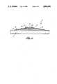
- FIG. 1depicts a cross-sectional side view of an overvoltage suppression device employing the stabilized threshold switching material of the present application.
- FIGS. 2A and 2Bare graphic representations of the observed values for first fire voltage and threshold voltage of non-stabilized and hydrogen stabilized chalcogenide glass switching materials, respectively.
- a method of fabricating an improved chalcogenide glass threshold switching materialcomprises an amorphous chalcogenide glass material which has been modified by exposure to a stabilizing element, preferably hydrogen.
- the methodis characterized by controllably exposing a stabilizing and uniformity-promoting element in preselected amounts, to the amorphous chalcogenide glass material at controlled temperatures, pressures and energy levels.
- the stabilizing and uniformity-promoting elementis exposed to the chalcogenide glass material from a precursor source of preferably molecular hydrogen, into a reactive environment.
- the improved threshold switching materialis characterized by substantially improved threshold switching stability and uniformity, particularly with respect to threshold voltage and first fire voltage.
- the inventors hereintheorize that the exposure of the chalcogenide glass materials to a hydrogenated atmosphere may modify said materials in one of two ways.
- One possibilityis that the hydrogen combines with chemical vacancies which exist due to the amorphous nature of the chalcogenide material. It is possible that the hydrogen, so combined, influences the energy and spatial distribution of the density of states in the chalcogenide glass material; thereby resulting in the modification of the recombination sites of the amorphous chalcogenide material.
- preliminary analysishas failed to show the incorporation of hydrogen into the host matrix of that chalcogenide material. Since detection by this analysis was limited to hydrogen incorporation exceeding 5-10%, it remains impossible to accurately reflect upon the degree or lack of hydrogen incorporation.
- the instant inventorsalso propose a second hypothesis, i.e., that the hydrogen from the atmosphere interacts with the chalcogenide glass material and bonds preferentially with oxygen present therein so as to form water (H 2 O) molecules.
- the H 2 O moleculesformed by the introduction of hydrogen, effuses during subsequent processing as during the anneal process, described hereinafter.
- the elimination of oxygen, a contaminant, from the materialcould also be responsible for the improved switching properties.
- FIGS. 2A and 2Bgraphically demonstrate the improvement in threshold switching stability and uniformity provided by subjecting chalcogenide glass materials to a hydrogenated atmosphere.
- FIGS. 2A and 2Brespectively, depict in graphic form, the switching stability and uniformity of non-stabilized and hydrogen stabilized (the specific fabrication techniques of which will be described in detail hereafter) chalcogenide glass material, having the nominal composition of Te 36 Ge 23 S 21 As 18 Se 2 .
- FIGS. 2A and 2Bare measurement graphs which plot voltage (as in first fire and threshold voltage) along the ordinate and cycles, which represents the number of times a device is subjected to a transient surge, along the abscissa.
- FIG. 2Athere is depicted therein a chart recording the first fire voltage and threshold voltage of a non-modified chalcogenide switching material over approximately 500 cycles.
- the observed value of the threshold voltage V this somewhat inconsistent, ranging from approximately 4.0 volts during the earlier cycles, up to approximately 6.0 volts with increased cycling, the average being about 5.1 volts.
- the observed first fire voltageis approximately 20.0 volts which is considerably higher than the voltage observed during subsequent cycles. It should be apparent that this lack of uniformity renders chalcogenide glass materials useless as surge suppressors. Further, because of the extremely high first fire voltage a number of "burn in” cycles is required before the non-modified device can be used. Additionally, these "burn-in” voltage cycles may in fact damage the device resulting in the long-term degradation observed for threshold voltage.
- FIG. 2Bthere is depicted therein a chart recording the threshold voltage and first fire voltage of a device employing a hydrogen stabilized chalcogenide glass material.
- the materialdisplays excellent stability and uniformity over many cycles, (approximately 1000). The observed values remain substantially constant during the entire cycling period, with an average threshold voltage of 9.4 volts.
- the first fire voltageis 8.70 volts, a value well within the range of average observed values, thus precluding the need for (and potential damage caused by), the "burn in" cycle.
- a device displaying stability and uniformity such as thiscan easily serve as a surge protection means since it can be reliably predicted to afford overvoltage protection at a given voltage, regardless of whether it is the first or 1000th overvoltage surge.
- FIGS. 2A and 2Bconclusively demonstrate the significant improvement in first fire and threshold switching stability and uniformity which may be achieved by subjecting chalcogenide glass materials to a stabilizing element such as hydrogen.
- the amorphous chalcogenide switching materialmay be subjected to the stabilizing element, such as hydrogen, in any number of methods, at least two of which are preferred and detailed hereinafter.
- the host matrix of the chalcogenide glass switching materialis subjected to a hydrogenated atmosphere as one step of a continuous deposition process. Specifically, during the sputtering of said chalcogenide switching material onto a substrate, hydrogenation can be established by providing an atmosphere of hydrogen gas in argon. The sputtering deposition of the glass material is preferably followed by a thermal anneal. The specific parameters for carrying out this process are set forth in detail in Example I which follows hereinafter.
- the second preferred method employed for subjecting the chalcogenide glass switching material to a hydrogenated atmosphereis a post deposition process which begins after the deposition of the chalcogenide glass material has been completed.
- a completed threshold switching deviceas depicted in FIG. 1, incorporating the thin film layer of chalcogenide material is subjected to a hydrogen plasma annealing process.
- This post deposition processrequires placing the chalcogenide switching material in an evacuated chamber which is operatively interconnected with a system capable of providing an annealing plasma.
- a source of hydrogen, preferably H 2 gasis introduced into the annealing system at a preselected flow rate, temperature and pressure and a plasma is initiated.
- the chalcogenide switching materialis then subjected to the annealing plasma for a period of time so as to allow for the reaction of at least a fractional atomic percentage of hydrogen with the chalcogenide glass material.
- the specific parameters for this annealing processare described in Example II.
- the exposure of the chalcogenide glass material to the hydrogenmay be limited by controlling the following parameters: the temperature, i.e., as in the annealing process temperature; the pressure within the reaction chamber; the energy level at which the exposure of the chalcogenide materials to hydrogen occurs; the flow rate of the precursor source of hydrogen; and the length of time during which the chalcogenide material is exposed to the hydrogenated atmosphere.
- the instant inventorshave been able to favorably modify the chalcogenide glass material. Further, through extensive experimentation, the instant inventors have developed a method for optimizing the switching characteristic in a given amorphous chalcogenide glass material.
- the threshold switching device 10includes a substrate 12 which may be either conductive or insulating, depending upon the specific use and location of said device.
- conductive substrate materials for the deviceinclude, but are not limited to, stainless steel, copper, aluminum and degenerately doped crystalline silicon; while suitable insulating substrates for the device include, but are not limited to, glass, crystalline silicon and crystal sapphire wafers.
- a highly conductive electrode 14formed of molybdenum, though other highly conductive metals such as graphite, refractory metal oxides, carbide, sulphide and tungsten may be employed with equal advantage.
- the electrode 14may be deposited to a thickness of about 1,500 to 25,000 Angstroms using any conventional or suitable technique such as sputtering, evaporation, vapor deposition, or the like.
- the electrodeis deposited as amorphous films by maintaining the substrates upon which they are deposited sufficiently cool so that the atoms condense into a generally disordered state upon contacting said surface.
- a thin film layer 16 of electrically conductive, phase stable, non-single crystal, non-switching carbonis deposited to a thickness of about 1,000 Angstroms, although thicknesses of about 100 Angstroms (to provide complete coverage of the electrode surface) up to about 5000 Angstroms are also preferred.
- each of the electrodes of the device 10are in intimate electrical contact with the superposed thin film layers of carbon such that current flows into one electrode through its respective carbon layer, through the active body of chalcogenide glass material, into the second layer of carbon and from there into the second electrode.
- the devicesmay also be constructed without the carbon layers, provided that the remaining electrodes are fully compatible with the body of chalcogenide glass material with which it is in contact.
- the layers of carbon 18are preferably deposited using d.c.-magnetron sputtering. Typical process parameters are a substrate temperature of about 100 degrees Centigrade, a pressure of about 0.5 pascal, a deposition rate of about 200-300 Angstroms per minute and a distance of approximately 6 cm. between the source and target.
- a pure (99.9 percent) carbon sourceis used so that the resultant film is substantially pure amorphous carbon.
- a layer of the hydrogen stabilized, thin film chalcogenide glass switching material 18is next deposited upon said thin film layer of carbon 16.
- the layer of chalcogenide glass material 18may be deposited to a thickness of approximately 100 (sufficient to obtain complete coverage of the carbon layer 16) to 50,000 Angstroms depending upon the magnitude of the threshold switching voltage desired.
- the thickness of the chalcogenide glass materialis related to the specified threshold voltage which is desired, and may be adjusted in a manner well understood in the art.
- the threshold voltage of threshold-type semiconductor materialsis approximately 30 volts per micron of conduction path length. Therefore, in order to achieve a threshold voltage on the order of 8 to 9 volts in a vertical threshold device of the type shown in FIG. 1, for example, the active layer is made approximately 3000 angstroms to 4000 angstroms thick.
- the chalcogenide glass materialis subjected to a hydrogenated atmosphere (hydrogen being the stabilizing and uniformity promoting element) either during the fabrication of the chalcogenide material itself, or during a subsequent, post deposition, anneal step.
- the preferred threshold switching materials from which the active layer is fabricatedinclude one or more chalcogen elements, i.e., sulphur, tellurium, and selenium.
- Preferred compositionsinclude, but are not limited to materials such as Te 36 Ge 23 S 21 As 18 Se 2 and other sulfur based chalcogenide glasses.
- a layer of insulating material 24, such as silicon oxide, silicon nitride, silicon carbon or siliconoxynitrideis deposited over the previously deposited layers so as to encapsulate the upper surface of the entire device.
- a via 26is then formed, as by conventional photolithographic techniques through said insulating layer 24 above a central portion of the upper electrode 22.
- a top conductive layer 28is deposited above said via, which conductive layer 28 may be patterned to provide means of communication with other small area devices also deposited on the common substrate 12 or otherwise electrically interconnected to other said devices within system.
- a preferred metal from which layer 28 is fabricatedis aluminum. It is to be noted that the inventive concept disclosed in the instant specification relates to surge suppression material characterized by improved stability and uniformity.
- current from the first electrode thereofpasses through at least one portion of the first carbon layer, through at least a filamentary path or portion of the chalcogenide glass material and through the second carbon film to the second electrode. Since current takes the path of least resistance, which should always be through the shortest or most direct route through material of uniform resistivity, the current conduction path in the thin carbon films and the semiconductor layer of FIG. 1 should be substantially vertical.
- the device 10it is preferred to deposit the multiple layers thereof in sequence while substrate 12 is continuously maintained under a partial vacuum. This helps ensure that extremely clean interfaces are formed between the layers, and greatly reduces the chance for any appreciable amount of contaminants such as air, water vapor, dust or the like to contaminate the interfaces. This not only helps ensure fine physical integrity of the interfaces, but also helps ensure the formation of high quality electrical interfaces between the layers. Such clean interfaces are believed to help greatly reduce possible localized heating effects and nucleation sites for undesired localized crystallization of the semiconductor materials, which may well adversely affect the electrical stability.
- the first method by which the host matrix of a thin film chalcogenide glass material is exposed to a hydrogenated atmospheredemonstrates that improved threshold switching can be obtained by subjecting the precursor constituent elements of that material to hydrogen during the actual deposition of said material onto a substrate.
- the chalcogenide glass materialis deposited by a reactive sputtering process of a type known in the art.
- the substrateis first cleaned as by conventional cleaning methods and then introduced into a vacuum deposition chamber under the following deposition conditions: chamber pressure is pumped down and held at about 0.2 pascal; a deposition rate of 100-300 angstroms per minute and a sputtering target comprising those materials to be sputtered into the substrate web, of approximately three inches in diameter.
- the power applied to said targetis approximately 42 watts thus yielding an applied power density of approximately 0.7 watts/square centimeter.
- a flow of approximately 1/2 percent hydrogen in argonis initiated and introduced into the sputtering chamber. This atmospheric concentration of hydrogen is maintained throughout the entire process of depositing the chalcogenide glass material, thus subjecting said material to the modifying element throughout the entire deposition thereof.
- the thickness of the chalcogenide materialis determined by the desired threshold voltage and can be altered by varying the length of time the chalcogenide deposition process remains operative.
- the sputtering processmay be followed immediately or at some subsequent time by a thermal annealing process adapted to further stabilize the properties of the hydrogenated chalcogenide glass material.
- a thermal annealing processadapted to further stabilize the properties of the hydrogenated chalcogenide glass material.
- the hydrogen stabilized materialis subjected to an annealing temperature of approximately 175-250 degrees Centigrade for 30 minutes.
- the hydrogen modified materialis then removed from the annealing temperature and allowed to cool.
- this annealprovides for the effusion of H 2 O therefrom.
- the second method by which the host matrix of a chalcogenide glass material may be subjected to a hydrogenated atmosphereinvolves a post deposition plasma annealing process employing the use of a hydrogen plasma atmosphere.
- the deposited layer of chalcogenide glass material of a Te 36 Ge 23 S 21 As 18 Se 2 compositionis placed into a conventional parallel plate plasma chamber which is operatively connected to a source of hydrogen gas (H 2 ).
- the chamberis cooled to and maintained at a temperature of approximately 25 degrees Centigrade and a pressure of 100 millitorr.
- a 50 sccm flow of hydrogen gas (H 2 )is started and an r.f. plasma is then initiated by the application of a 200 watt source of applied power.
- the plasmawas maintained for approximately 3.5 minutes and then extinguished.
- the flow of gasesis then terminated and the chamber is flooded with argon.
Landscapes
- Engineering & Computer Science (AREA)
- Manufacturing & Machinery (AREA)
- Glass Compositions (AREA)
Abstract
Description
______________________________________ 3,271,591 3,571,671 3,343,034 3,571,672 3,571,669 3,588,638 3,571,670 3,611,063 ______________________________________
Claims (10)
Priority Applications (1)
| Application Number | Priority Date | Filing Date | Title |
|---|---|---|---|
| US07/107,318US4804490A (en) | 1987-10-13 | 1987-10-13 | Method of fabricating stabilized threshold switching material |
Applications Claiming Priority (1)
| Application Number | Priority Date | Filing Date | Title |
|---|---|---|---|
| US07/107,318US4804490A (en) | 1987-10-13 | 1987-10-13 | Method of fabricating stabilized threshold switching material |
Publications (1)
| Publication Number | Publication Date |
|---|---|
| US4804490Atrue US4804490A (en) | 1989-02-14 |
Family
ID=22316020
Family Applications (1)
| Application Number | Title | Priority Date | Filing Date |
|---|---|---|---|
| US07/107,318Expired - LifetimeUS4804490A (en) | 1987-10-13 | 1987-10-13 | Method of fabricating stabilized threshold switching material |
Country Status (1)
| Country | Link |
|---|---|
| US (1) | US4804490A (en) |
Cited By (50)
| Publication number | Priority date | Publication date | Assignee | Title |
|---|---|---|---|---|
| US5177567A (en)* | 1991-07-19 | 1993-01-05 | Energy Conversion Devices, Inc. | Thin-film structure for chalcogenide electrical switching devices and process therefor |
| EP0494074A3 (en)* | 1991-01-02 | 1994-01-19 | Energy Conversion Devices Inc | |
| US5330616A (en)* | 1988-02-01 | 1994-07-19 | Semiconductor Energy Laboratory Co., Ltd. | Electric device provided with carbon pattern structure and manufacturing method for the same |
| US5751012A (en)* | 1995-06-07 | 1998-05-12 | Micron Technology, Inc. | Polysilicon pillar diode for use in a non-volatile memory cell |
| US5753947A (en)* | 1995-01-20 | 1998-05-19 | Micron Technology, Inc. | Very high-density DRAM cell structure and method for fabricating it |
| US5789277A (en)* | 1996-07-22 | 1998-08-04 | Micron Technology, Inc. | Method of making chalogenide memory device |
| US5812441A (en)* | 1996-10-21 | 1998-09-22 | Micron Technology, Inc. | MOS diode for use in a non-volatile memory cell |
| US5814527A (en)* | 1996-07-22 | 1998-09-29 | Micron Technology, Inc. | Method of making small pores defined by a disposable internal spacer for use in chalcogenide memories |
| US5831276A (en)* | 1995-06-07 | 1998-11-03 | Micron Technology, Inc. | Three-dimensional container diode for use with multi-state material in a non-volatile memory cell |
| US5837564A (en)* | 1995-11-01 | 1998-11-17 | Micron Technology, Inc. | Method for optimal crystallization to obtain high electrical performance from chalcogenides |
| US5841150A (en)* | 1995-06-07 | 1998-11-24 | Micron Technology, Inc. | Stack/trench diode for use with a muti-state material in a non-volatile memory cell |
| US5869808A (en)* | 1992-11-09 | 1999-02-09 | American Roller Company | Ceramic heater roller and methods of making same |
| US5869843A (en)* | 1995-06-07 | 1999-02-09 | Micron Technology, Inc. | Memory array having a multi-state element and method for forming such array or cells thereof |
| US5879955A (en)* | 1995-06-07 | 1999-03-09 | Micron Technology, Inc. | Method for fabricating an array of ultra-small pores for chalcogenide memory cells |
| US5920788A (en)* | 1995-06-07 | 1999-07-06 | Micron Technology, Inc. | Chalcogenide memory cell with a plurality of chalcogenide electrodes |
| US5952671A (en)* | 1997-05-09 | 1999-09-14 | Micron Technology, Inc. | Small electrode for a chalcogenide switching device and method for fabricating same |
| US5970336A (en)* | 1996-08-22 | 1999-10-19 | Micron Technology, Inc. | Method of making memory cell incorporating a chalcogenide element |
| US5985698A (en)* | 1996-07-22 | 1999-11-16 | Micron Technology, Inc. | Fabrication of three dimensional container diode for use with multi-state material in a non-volatile memory cell |
| US6015977A (en)* | 1997-01-28 | 2000-01-18 | Micron Technology, Inc. | Integrated circuit memory cell having a small active area and method of forming same |
| USRE36518E (en)* | 1992-06-23 | 2000-01-18 | Micron Technology, Inc. | Method for making electrical contact with an active area through sub-micron contact openings and a semiconductor device |
| US6025220A (en)* | 1996-06-18 | 2000-02-15 | Micron Technology, Inc. | Method of forming a polysilicon diode and devices incorporating such diode |
| US6031287A (en)* | 1997-06-18 | 2000-02-29 | Micron Technology, Inc. | Contact structure and memory element incorporating the same |
| US6087689A (en)* | 1997-06-16 | 2000-07-11 | Micron Technology, Inc. | Memory cell having a reduced active area and a memory array incorporating the same |
| US6115090A (en)* | 1997-03-26 | 2000-09-05 | Semiconductor Energy Laboratory Co., Ltd. | Display device |
| US6117720A (en)* | 1995-06-07 | 2000-09-12 | Micron Technology, Inc. | Method of making an integrated circuit electrode having a reduced contact area |
| US6130103A (en)* | 1998-04-17 | 2000-10-10 | Symetrix Corporation | Method for fabricating ferroelectric integrated circuits |
| US6337266B1 (en) | 1996-07-22 | 2002-01-08 | Micron Technology, Inc. | Small electrode for chalcogenide memories |
| US6440837B1 (en) | 2000-07-14 | 2002-08-27 | Micron Technology, Inc. | Method of forming a contact structure in a semiconductor device |
| KR100354782B1 (en)* | 1995-11-28 | 2002-11-18 | 에너지 컨버젼 디바이시즈, 아이엔씨. | Integrated drivers for flat panel displays employing chalcogenide logic elements |
| US20030047772A1 (en)* | 2001-03-15 | 2003-03-13 | Jiutao Li | Agglomeration elimination for metal sputter deposition of chalcogenides |
| US6563156B2 (en) | 2001-03-15 | 2003-05-13 | Micron Technology, Inc. | Memory elements and methods for making same |
| US20030155606A1 (en)* | 2002-02-15 | 2003-08-21 | Campbell Kristy A. | Method to alter chalcogenide glass for improved switching characteristics |
| US20030194865A1 (en)* | 2002-04-10 | 2003-10-16 | Gilton Terry L. | Method of manufacture of programmable conductor memory |
| US20030193053A1 (en)* | 2002-04-10 | 2003-10-16 | Gilton Terry L. | Thin film diode integrated with chalcogenide memory cell |
| US6670713B2 (en) | 1996-02-23 | 2003-12-30 | Micron Technology, Inc. | Method for forming conductors in semiconductor devices |
| US20040038480A1 (en)* | 2002-08-22 | 2004-02-26 | Moore John T. | Method of manufacture of a PCRAM memory cell |
| US6718272B1 (en)* | 2000-11-01 | 2004-04-06 | Eni Technology Inc. | Fast transient protection for RF plasma generator |
| US20040179346A1 (en)* | 2003-03-12 | 2004-09-16 | Michael Brooks | Electro-magnetic suppressive structure |
| US20040257848A1 (en)* | 2003-06-18 | 2004-12-23 | Macronix International Co., Ltd. | Method for adjusting the threshold voltage of a memory cell |
| US20040266172A1 (en)* | 2003-06-30 | 2004-12-30 | Kim Tae Kyung | Method for forming metal lines |
| US6927826B2 (en) | 1997-03-26 | 2005-08-09 | Semiconductor Energy Labaratory Co., Ltd. | Display device |
| US20050202588A1 (en)* | 2004-03-10 | 2005-09-15 | Brooks Joseph F. | Method of forming a chalcogenide material containing device |
| US20050200767A1 (en)* | 1999-03-29 | 2005-09-15 | Semiconductor Energy Laboratory Co., Ltd. | Semiconductor device and manufacturing method thereof |
| US20060126254A1 (en)* | 2004-12-14 | 2006-06-15 | Stmicroelectronics Sa | Protection of an integrated capacitor |
| US20070181928A1 (en)* | 2005-08-24 | 2007-08-09 | Yoshiki Yamanishi | Capacitor and manufacturing method thereof |
| US7508033B2 (en) | 1998-04-24 | 2009-03-24 | Semiconductor Energy Laboratory Co., Ltd. | Semiconductor device with diamond-like carbon film on backside of substrate |
| USRE40790E1 (en)* | 1992-06-23 | 2009-06-23 | Micron Technology, Inc. | Method for making electrical contact with an active area through sub-micron contact openings and a semiconductor device |
| US20140347772A1 (en)* | 2013-05-23 | 2014-11-27 | Inpaq Technology Co., Ltd. | Over-voltage protection device and method for preparing the same |
| US9306166B1 (en)* | 2015-01-28 | 2016-04-05 | SK Hynix Inc. | Fabrication method of resistance variable memory apparatus |
| CN110729087A (en)* | 2019-10-18 | 2020-01-24 | 大连理工大学 | A voltage control material resistance change curve controllable combination device and realization method |
Citations (7)
| Publication number | Priority date | Publication date | Assignee | Title |
|---|---|---|---|---|
| US4040917A (en)* | 1975-07-02 | 1977-08-09 | Exxon Research And Engineering Company | Preparation of intercalated chalcogenides |
| US4217374A (en)* | 1978-03-08 | 1980-08-12 | Energy Conversion Devices, Inc. | Amorphous semiconductors equivalent to crystalline semiconductors |
| SU679025A1 (en)* | 1977-08-03 | 1981-08-07 | Предприятие П/Я А-3603 | Method of manufacturing temperature-sensitive semi-conductor elements |
| JPS56125847A (en)* | 1980-03-07 | 1981-10-02 | Chiyou Lsi Gijutsu Kenkyu Kumiai | Surface treatment of semiconductor |
| US4375125A (en)* | 1980-03-07 | 1983-03-01 | U.S. Philips Corporation | Method of passivating pn-junction in a semiconductor device |
| JPS5956575A (en)* | 1982-09-27 | 1984-04-02 | Nec Corp | Method for implanting ion |
| US4610731A (en)* | 1985-04-03 | 1986-09-09 | At&T Bell Laboratories | Shallow impurity neutralization |
- 1987
- 1987-10-13USUS07/107,318patent/US4804490A/ennot_activeExpired - Lifetime
Patent Citations (7)
| Publication number | Priority date | Publication date | Assignee | Title |
|---|---|---|---|---|
| US4040917A (en)* | 1975-07-02 | 1977-08-09 | Exxon Research And Engineering Company | Preparation of intercalated chalcogenides |
| SU679025A1 (en)* | 1977-08-03 | 1981-08-07 | Предприятие П/Я А-3603 | Method of manufacturing temperature-sensitive semi-conductor elements |
| US4217374A (en)* | 1978-03-08 | 1980-08-12 | Energy Conversion Devices, Inc. | Amorphous semiconductors equivalent to crystalline semiconductors |
| JPS56125847A (en)* | 1980-03-07 | 1981-10-02 | Chiyou Lsi Gijutsu Kenkyu Kumiai | Surface treatment of semiconductor |
| US4375125A (en)* | 1980-03-07 | 1983-03-01 | U.S. Philips Corporation | Method of passivating pn-junction in a semiconductor device |
| JPS5956575A (en)* | 1982-09-27 | 1984-04-02 | Nec Corp | Method for implanting ion |
| US4610731A (en)* | 1985-04-03 | 1986-09-09 | At&T Bell Laboratories | Shallow impurity neutralization |
Non-Patent Citations (2)
| Title |
|---|
| Smeets et al., "Passivation of Silicon p-n Junctions by Sightly Conductive Chalcogenide Films", J. Electrochem. Soc.: Solid-State Science and Technology, Sep. 1977, pp. 1458-1459. |
| Smeets et al., Passivation of Silicon p n Junctions by Sightly Conductive Chalcogenide Films , J. Electrochem. Soc.: Solid State Science and Technology, Sep. 1977, pp. 1458 1459.* |
Cited By (143)
| Publication number | Priority date | Publication date | Assignee | Title |
|---|---|---|---|---|
| US5330616A (en)* | 1988-02-01 | 1994-07-19 | Semiconductor Energy Laboratory Co., Ltd. | Electric device provided with carbon pattern structure and manufacturing method for the same |
| EP0494074A3 (en)* | 1991-01-02 | 1994-01-19 | Energy Conversion Devices Inc | |
| US5330630A (en)* | 1991-01-02 | 1994-07-19 | Energy Conversion Devices, Inc. | Switch with improved threshold voltage |
| US5177567A (en)* | 1991-07-19 | 1993-01-05 | Energy Conversion Devices, Inc. | Thin-film structure for chalcogenide electrical switching devices and process therefor |
| USRE36518E (en)* | 1992-06-23 | 2000-01-18 | Micron Technology, Inc. | Method for making electrical contact with an active area through sub-micron contact openings and a semiconductor device |
| USRE40790E1 (en)* | 1992-06-23 | 2009-06-23 | Micron Technology, Inc. | Method for making electrical contact with an active area through sub-micron contact openings and a semiconductor device |
| US5869808A (en)* | 1992-11-09 | 1999-02-09 | American Roller Company | Ceramic heater roller and methods of making same |
| US6096596A (en)* | 1995-01-20 | 2000-08-01 | Micron Technology Inc. | Very high-density DRAM cell structure and method for fabricating it |
| US5753947A (en)* | 1995-01-20 | 1998-05-19 | Micron Technology, Inc. | Very high-density DRAM cell structure and method for fabricating it |
| US20100184258A1 (en)* | 1995-06-07 | 2010-07-22 | Round Rock Research Llc | Method and apparatus for forming an integrated circuit electrode having a reduced contact area |
| US7687796B2 (en) | 1995-06-07 | 2010-03-30 | Micron Technology, Inc. | Method and apparatus for forming an integrated circuit electrode having a reduced contact area |
| US5841150A (en)* | 1995-06-07 | 1998-11-24 | Micron Technology, Inc. | Stack/trench diode for use with a muti-state material in a non-volatile memory cell |
| US5831276A (en)* | 1995-06-07 | 1998-11-03 | Micron Technology, Inc. | Three-dimensional container diode for use with multi-state material in a non-volatile memory cell |
| US5869843A (en)* | 1995-06-07 | 1999-02-09 | Micron Technology, Inc. | Memory array having a multi-state element and method for forming such array or cells thereof |
| US5879955A (en)* | 1995-06-07 | 1999-03-09 | Micron Technology, Inc. | Method for fabricating an array of ultra-small pores for chalcogenide memory cells |
| US5920788A (en)* | 1995-06-07 | 1999-07-06 | Micron Technology, Inc. | Chalcogenide memory cell with a plurality of chalcogenide electrodes |
| US6831330B2 (en) | 1995-06-07 | 2004-12-14 | Micron Technology, Inc. | Method and apparatus for forming an integrated circuit electrode having a reduced contact area |
| US6797978B2 (en) | 1995-06-07 | 2004-09-28 | Micron Technology, Inc. | Method for fabricating an array of ultra-small pores for chalcogenide memory cells |
| US20050029587A1 (en)* | 1995-06-07 | 2005-02-10 | Harshfield Steven T. | Method and apparatus for forming an integrated circuit electrode having a reduced contact area |
| US20040161895A1 (en)* | 1995-06-07 | 2004-08-19 | Fernando Gonzalez | Method for fabricating an array of ultra-small pores for chalcogenide memory cells |
| US7271440B2 (en) | 1995-06-07 | 2007-09-18 | Micron Technology, Inc. | Method and apparatus for forming an integrated circuit electrode having a reduced contact area |
| US6002140A (en)* | 1995-06-07 | 1999-12-14 | Micron Technology, Inc. | Method for fabricating an array of ultra-small pores for chalcogenide memory cells |
| US6429449B1 (en) | 1995-06-07 | 2002-08-06 | Micron Technology, Inc. | Three-dimensional container diode for use with multi-state material in a non-volatile memory cell |
| US6916710B2 (en) | 1995-06-07 | 2005-07-12 | Micron Technology, Inc. | Method for fabricating an array of ultra-small pores for chalcogenide memory cells |
| US6391688B1 (en) | 1995-06-07 | 2002-05-21 | Micron Technology, Inc. | Method for fabricating an array of ultra-small pores for chalcogenide memory cells |
| US6420725B1 (en) | 1995-06-07 | 2002-07-16 | Micron Technology, Inc. | Method and apparatus for forming an integrated circuit electrode having a reduced contact area |
| US6077729A (en)* | 1995-06-07 | 2000-06-20 | Micron Technology, Inc. | Memory array having a multi-state element and method for forming such array or cellis thereof |
| US6653195B1 (en) | 1995-06-07 | 2003-11-25 | Micron Technology, Inc. | Fabrication of three dimensional container diode for use with multi-state material in a non-volatile memory cell |
| US5751012A (en)* | 1995-06-07 | 1998-05-12 | Micron Technology, Inc. | Polysilicon pillar diode for use in a non-volatile memory cell |
| US6104038A (en)* | 1995-06-07 | 2000-08-15 | Micron Technology, Inc. | Method for fabricating an array of ultra-small pores for chalcogenide memory cells |
| US20010055874A1 (en)* | 1995-06-07 | 2001-12-27 | Fernando Gonzalez | Method for fabricating an array of ultra-small pores for chalcogenide memory cells |
| US20020179896A1 (en)* | 1995-06-07 | 2002-12-05 | Harshfield Steven T. | Method and apparatus for forming an integrated circuit electrode having a reduced contact area |
| US8017453B2 (en) | 1995-06-07 | 2011-09-13 | Round Rock Research, Llc | Method and apparatus for forming an integrated circuit electrode having a reduced contact area |
| US6117720A (en)* | 1995-06-07 | 2000-09-12 | Micron Technology, Inc. | Method of making an integrated circuit electrode having a reduced contact area |
| US6118135A (en)* | 1995-06-07 | 2000-09-12 | Micron Technology, Inc. | Three-dimensional container diode for use with multi-state material in a non-volatile memory cell |
| US6534780B1 (en) | 1995-06-07 | 2003-03-18 | Micron Technology, Inc. | Array of ultra-small pores for memory cells |
| US5837564A (en)* | 1995-11-01 | 1998-11-17 | Micron Technology, Inc. | Method for optimal crystallization to obtain high electrical performance from chalcogenides |
| EP0864204B1 (en)* | 1995-11-28 | 2003-09-24 | Energy Conversion Devices, Inc. | Integrated drivers for flat panel displays employing chalcogenide logic elements |
| KR100354782B1 (en)* | 1995-11-28 | 2002-11-18 | 에너지 컨버젼 디바이시즈, 아이엔씨. | Integrated drivers for flat panel displays employing chalcogenide logic elements |
| US6670713B2 (en) | 1996-02-23 | 2003-12-30 | Micron Technology, Inc. | Method for forming conductors in semiconductor devices |
| US6700211B2 (en) | 1996-02-23 | 2004-03-02 | Micron Technology, Inc. | Method for forming conductors in semiconductor devices |
| US6025220A (en)* | 1996-06-18 | 2000-02-15 | Micron Technology, Inc. | Method of forming a polysilicon diode and devices incorporating such diode |
| US6392913B1 (en) | 1996-06-18 | 2002-05-21 | Micron Technology, Inc. | Method of forming a polysilicon diode and devices incorporating such diode |
| US6229157B1 (en) | 1996-06-18 | 2001-05-08 | Micron Technology, Inc. | Method of forming a polysilicon diode and devices incorporating such diode |
| US6111264A (en)* | 1996-07-22 | 2000-08-29 | Micron Technology, Inc. | Small pores defined by a disposable internal spacer for use in chalcogenide memories |
| US20100151665A1 (en)* | 1996-07-22 | 2010-06-17 | Micron Technology, Inc | Small electrode for phase change memories |
| US7494922B2 (en) | 1996-07-22 | 2009-02-24 | Micron Technology, Inc. | Small electrode for phase change memories |
| US5789277A (en)* | 1996-07-22 | 1998-08-04 | Micron Technology, Inc. | Method of making chalogenide memory device |
| US6316784B1 (en) | 1996-07-22 | 2001-11-13 | Micron Technology, Inc. | Method of making chalcogenide memory device |
| US7273809B2 (en) | 1996-07-22 | 2007-09-25 | Micron Technology, Inc. | Method of fabricating a conductive path in a semiconductor device |
| US8264061B2 (en) | 1996-07-22 | 2012-09-11 | Round Rock Research, Llc | Phase change memory cell and devices containing same |
| US20050042862A1 (en)* | 1996-07-22 | 2005-02-24 | Zahorik Russell C. | Small electrode for chalcogenide memories |
| US7687881B2 (en) | 1996-07-22 | 2010-03-30 | Micron Technology, Inc. | Small electrode for phase change memories |
| US6492656B2 (en) | 1996-07-22 | 2002-12-10 | Micron Technology, Inc | Reduced mask chalcogenide memory |
| US6531391B2 (en) | 1996-07-22 | 2003-03-11 | Micron Technology, Inc. | Method of fabricating a conductive path in a semiconductor device |
| US5985698A (en)* | 1996-07-22 | 1999-11-16 | Micron Technology, Inc. | Fabrication of three dimensional container diode for use with multi-state material in a non-volatile memory cell |
| US6337266B1 (en) | 1996-07-22 | 2002-01-08 | Micron Technology, Inc. | Small electrode for chalcogenide memories |
| US6635951B1 (en) | 1996-07-22 | 2003-10-21 | Micron Technology, Inc. | Small electrode for chalcogenide memories |
| US5814527A (en)* | 1996-07-22 | 1998-09-29 | Micron Technology, Inc. | Method of making small pores defined by a disposable internal spacer for use in chalcogenide memories |
| US6797612B2 (en) | 1996-07-22 | 2004-09-28 | Micron Technology, Inc. | Method of fabricating a small electrode for chalcogenide memory cells |
| US20110042640A1 (en)* | 1996-07-22 | 2011-02-24 | Round Rock Research, Llc | Method of fabricating phase change memory cell |
| US7838416B2 (en) | 1996-07-22 | 2010-11-23 | Round Rock Research, Llc | Method of fabricating phase change memory cell |
| US5970336A (en)* | 1996-08-22 | 1999-10-19 | Micron Technology, Inc. | Method of making memory cell incorporating a chalcogenide element |
| US5998244A (en)* | 1996-08-22 | 1999-12-07 | Micron Technology, Inc. | Memory cell incorporating a chalcogenide element and method of making same |
| US6153890A (en)* | 1996-08-22 | 2000-11-28 | Micron Technology, Inc. | Memory cell incorporating a chalcogenide element |
| US5978258A (en)* | 1996-10-21 | 1999-11-02 | Micron Technology, Inc. | MOS diode for use in a non-volatile memory cell background |
| US5812441A (en)* | 1996-10-21 | 1998-09-22 | Micron Technology, Inc. | MOS diode for use in a non-volatile memory cell |
| US6534368B2 (en) | 1997-01-28 | 2003-03-18 | Micron Technology, Inc. | Integrated circuit memory cell having a small active area and method of forming same |
| US6114713A (en)* | 1997-01-28 | 2000-09-05 | Zahorik; Russell C. | Integrated circuit memory cell having a small active area and method of forming same |
| US6287919B1 (en) | 1997-01-28 | 2001-09-11 | Micron Technology, Inc. | Integrated circuit memory cell having a small active area and method of forming same |
| US6015977A (en)* | 1997-01-28 | 2000-01-18 | Micron Technology, Inc. | Integrated circuit memory cell having a small active area and method of forming same |
| US20050264740A1 (en)* | 1997-03-26 | 2005-12-01 | Semiconductor Energy Laboratory Co., Ltd. | Display device |
| US6115090A (en)* | 1997-03-26 | 2000-09-05 | Semiconductor Energy Laboratory Co., Ltd. | Display device |
| US6927826B2 (en) | 1997-03-26 | 2005-08-09 | Semiconductor Energy Labaratory Co., Ltd. | Display device |
| US7190428B2 (en) | 1997-03-26 | 2007-03-13 | Semiconductor Energy Laboratory Co., Ltd. | Display device |
| US20070263133A1 (en)* | 1997-03-26 | 2007-11-15 | Semiconductor Energy Laboratory Co., Ltd. | Display device |
| US7436463B2 (en) | 1997-03-26 | 2008-10-14 | Semiconductor Energy Laboratory Co., Ltd. | Display device |
| US6593990B1 (en) | 1997-03-26 | 2003-07-15 | Semiconductor Energy Laboratory Co., Ltd. | Display device |
| US6189582B1 (en) | 1997-05-09 | 2001-02-20 | Micron Technology, Inc. | Small electrode for a chalcogenide switching device and method for fabricating same |
| US20060261380A1 (en)* | 1997-05-09 | 2006-11-23 | Reinberg Alan R | Small electrode for a chalcogenide switching device and method for fabricating same |
| US5952671A (en)* | 1997-05-09 | 1999-09-14 | Micron Technology, Inc. | Small electrode for a chalcogenide switching device and method for fabricating same |
| US7453082B2 (en) | 1997-05-09 | 2008-11-18 | Micron Technology, Inc. | Small electrode for a chalcogenide switching device and method for fabricating same |
| US6777705B2 (en) | 1997-05-09 | 2004-08-17 | Micron Technology, Inc. | X-point memory cell |
| US20080055973A1 (en)* | 1997-05-09 | 2008-03-06 | Micron Technology Inc. | Small Electrode for a Chacogenide Switching Device and Method for Fabricating Same |
| US20010002046A1 (en)* | 1997-05-09 | 2001-05-31 | Reinberg Alan R. | Small electrode for a chalcogenide switching device and method for fabricating same |
| US6225142B1 (en) | 1997-06-16 | 2001-05-01 | Micron Technology, Inc. | Memory cell having a reduced active area and a memory array incorporating the same |
| US6252244B1 (en) | 1997-06-16 | 2001-06-26 | Micron Technology, Inc. | Memory cell having a reduced active area and a memory array incorporating the same |
| US6087689A (en)* | 1997-06-16 | 2000-07-11 | Micron Technology, Inc. | Memory cell having a reduced active area and a memory array incorporating the same |
| US6031287A (en)* | 1997-06-18 | 2000-02-29 | Micron Technology, Inc. | Contact structure and memory element incorporating the same |
| US6130103A (en)* | 1998-04-17 | 2000-10-10 | Symetrix Corporation | Method for fabricating ferroelectric integrated circuits |
| US7508033B2 (en) | 1998-04-24 | 2009-03-24 | Semiconductor Energy Laboratory Co., Ltd. | Semiconductor device with diamond-like carbon film on backside of substrate |
| US8093591B2 (en) | 1999-03-29 | 2012-01-10 | Semiconductor Energy Laboratory Co., Ltd. | Semiconductor device and manufacturing method thereof |
| US20100155732A1 (en)* | 1999-03-29 | 2010-06-24 | Semiconductor Energy Laboratory Co. Ltd. | Semiconductor Device and Manufacturing Method Thereof |
| US7633085B2 (en) | 1999-03-29 | 2009-12-15 | Semiconductor Energy Laboratory Co., Ltd. | Semiconductor device and manufacturing method thereof |
| US20050200767A1 (en)* | 1999-03-29 | 2005-09-15 | Semiconductor Energy Laboratory Co., Ltd. | Semiconductor device and manufacturing method thereof |
| US20040124503A1 (en)* | 2000-07-14 | 2004-07-01 | Harshfield Steven T. | Memory elements and methods for making same |
| US7504730B2 (en) | 2000-07-14 | 2009-03-17 | Micron Technology, Inc. | Memory elements |
| US20090152737A1 (en)* | 2000-07-14 | 2009-06-18 | Micron Technology, Inc. | Memory devices having contact features |
| US8786101B2 (en) | 2000-07-14 | 2014-07-22 | Round Rock Research, Llc | Contact structure in a memory device |
| US8362625B2 (en) | 2000-07-14 | 2013-01-29 | Round Rock Research, Llc | Contact structure in a memory device |
| US6440837B1 (en) | 2000-07-14 | 2002-08-27 | Micron Technology, Inc. | Method of forming a contact structure in a semiconductor device |
| USRE40842E1 (en)* | 2000-07-14 | 2009-07-14 | Micron Technology, Inc. | Memory elements and methods for making same |
| US8076783B2 (en) | 2000-07-14 | 2011-12-13 | Round Rock Research, Llc | Memory devices having contact features |
| US6607974B2 (en) | 2000-07-14 | 2003-08-19 | Micron Technology, Inc. | Method of forming a contact structure in a semiconductor device |
| US20080017953A9 (en)* | 2000-07-14 | 2008-01-24 | Harshfield Steven T | Memory elements and methods for making same |
| US6718272B1 (en)* | 2000-11-01 | 2004-04-06 | Eni Technology Inc. | Fast transient protection for RF plasma generator |
| US6878569B2 (en) | 2001-03-15 | 2005-04-12 | Micron Technology, Inc. | Agglomeration elimination for metal sputter deposition of chalcogenides |
| US6949453B2 (en) | 2001-03-15 | 2005-09-27 | Micron Technology, Inc. | Agglomeration elimination for metal sputter deposition of chalcogenides |
| US6563156B2 (en) | 2001-03-15 | 2003-05-13 | Micron Technology, Inc. | Memory elements and methods for making same |
| US20040144968A1 (en)* | 2001-03-15 | 2004-07-29 | Jiutao Li | Agglomeration elimination for metal sputter deposition of chalcogenides |
| US20040144973A1 (en)* | 2001-03-15 | 2004-07-29 | Jiutao Li | Agglomeration elimination for metal sputter deposition of chalcogenides |
| US20030047772A1 (en)* | 2001-03-15 | 2003-03-13 | Jiutao Li | Agglomeration elimination for metal sputter deposition of chalcogenides |
| US6974965B2 (en) | 2001-03-15 | 2005-12-13 | Micron Technology, Inc. | Agglomeration elimination for metal sputter deposition of chalcogenides |
| US7528401B2 (en) | 2001-03-15 | 2009-05-05 | Micron Technology, Inc. | Agglomeration elimination for metal sputter deposition of chalcogenides |
| US6867064B2 (en)* | 2002-02-15 | 2005-03-15 | Micron Technology, Inc. | Method to alter chalcogenide glass for improved switching characteristics |
| US20030155606A1 (en)* | 2002-02-15 | 2003-08-21 | Campbell Kristy A. | Method to alter chalcogenide glass for improved switching characteristics |
| US20030194865A1 (en)* | 2002-04-10 | 2003-10-16 | Gilton Terry L. | Method of manufacture of programmable conductor memory |
| US6855975B2 (en) | 2002-04-10 | 2005-02-15 | Micron Technology, Inc. | Thin film diode integrated with chalcogenide memory cell |
| US6858482B2 (en) | 2002-04-10 | 2005-02-22 | Micron Technology, Inc. | Method of manufacture of programmable switching circuits and memory cells employing a glass layer |
| US7479650B2 (en) | 2002-04-10 | 2009-01-20 | Micron Technology, Inc. | Method of manufacture of programmable conductor memory |
| US20030193053A1 (en)* | 2002-04-10 | 2003-10-16 | Gilton Terry L. | Thin film diode integrated with chalcogenide memory cell |
| US20040171208A1 (en)* | 2002-04-10 | 2004-09-02 | Gilton Terry L. | Method of manufacture of programmable conductor memory |
| US7459764B2 (en) | 2002-08-22 | 2008-12-02 | Micron Technology, Inc. | Method of manufacture of a PCRAM memory cell |
| US20040238918A1 (en)* | 2002-08-22 | 2004-12-02 | Moore John T. | Method of manufacture of a PCRAM memory cell |
| US20040038480A1 (en)* | 2002-08-22 | 2004-02-26 | Moore John T. | Method of manufacture of a PCRAM memory cell |
| US7018863B2 (en) | 2002-08-22 | 2006-03-28 | Micron Technology, Inc. | Method of manufacture of a resistance variable memory cell |
| US20040179346A1 (en)* | 2003-03-12 | 2004-09-16 | Michael Brooks | Electro-magnetic suppressive structure |
| US7248484B2 (en)* | 2003-03-12 | 2007-07-24 | Hewlett-Packard Development Company, L.P. | Electro-magnetic suppressive structure |
| US20040257848A1 (en)* | 2003-06-18 | 2004-12-23 | Macronix International Co., Ltd. | Method for adjusting the threshold voltage of a memory cell |
| CN100505362C (en)* | 2003-06-18 | 2009-06-24 | 旺宏电子股份有限公司 | Method for adjusting threshold voltage of memory cell and chalcogenide material |
| US20040266172A1 (en)* | 2003-06-30 | 2004-12-30 | Kim Tae Kyung | Method for forming metal lines |
| US6921717B2 (en) | 2003-06-30 | 2005-07-26 | Hynix Semiconductor Inc. | Method for forming metal lines |
| US7459336B2 (en) | 2004-03-10 | 2008-12-02 | Micron Technology, Inc. | Method of forming a chalcogenide material containing device |
| US20050202588A1 (en)* | 2004-03-10 | 2005-09-15 | Brooks Joseph F. | Method of forming a chalcogenide material containing device |
| US20060246696A1 (en)* | 2004-03-10 | 2006-11-02 | Micron Technology, Inc. | Method of forming a chalcogenide material containing device |
| US7098068B2 (en) | 2004-03-10 | 2006-08-29 | Micron Technology, Inc. | Method of forming a chalcogenide material containing device |
| US20060126254A1 (en)* | 2004-12-14 | 2006-06-15 | Stmicroelectronics Sa | Protection of an integrated capacitor |
| US8247289B2 (en)* | 2005-08-24 | 2012-08-21 | Ibiden Co., Ltd. | Capacitor and manufacturing method thereof |
| US20070181928A1 (en)* | 2005-08-24 | 2007-08-09 | Yoshiki Yamanishi | Capacitor and manufacturing method thereof |
| US20140347772A1 (en)* | 2013-05-23 | 2014-11-27 | Inpaq Technology Co., Ltd. | Over-voltage protection device and method for preparing the same |
| US9099861B2 (en)* | 2013-05-23 | 2015-08-04 | Inpaq Technology Co., Ltd. | Over-voltage protection device and method for preparing the same |
| US9306166B1 (en)* | 2015-01-28 | 2016-04-05 | SK Hynix Inc. | Fabrication method of resistance variable memory apparatus |
| CN110729087A (en)* | 2019-10-18 | 2020-01-24 | 大连理工大学 | A voltage control material resistance change curve controllable combination device and realization method |
Similar Documents
| Publication | Publication Date | Title |
|---|---|---|
| US4804490A (en) | Method of fabricating stabilized threshold switching material | |
| US4809044A (en) | Thin film overvoltage protection devices | |
| JP2542875B2 (en) | Thin film electric device having amorphous carbon electrode and method of manufacturing the same | |
| Hong et al. | Switching behavior in II-IV-V2 amorphous semiconductor systems | |
| US5614727A (en) | Thin film diode having large current capability with low turn-on voltages for integrated devices | |
| EP0494074B1 (en) | Switch with improved threshold voltage | |
| CA1313569C (en) | Electrical switching device | |
| KR101173333B1 (en) | Device for converting thermal energy into electrical energy | |
| Coward | Experimental evidence of filament “forming” in non-crystalline chalcogenide alloy threshold switches | |
| US3962715A (en) | High-speed, high-current spike suppressor and method for fabricating same | |
| US4121240A (en) | Semiconductor device having a discharge-formed insulating film | |
| Yoneda et al. | The grain size dependence of the mobility and lifetime in chemical vapor deposited diamond photoconductive switches | |
| US6614178B1 (en) | Solid-state excimer devices and processes for producing same | |
| US20100097735A1 (en) | Method of protecting and dissipating electrostatic discharges in an integrated circuit | |
| EP0242902A2 (en) | Protection device | |
| KR102432688B1 (en) | multi-layered selector device and method of manufacturing the same | |
| JP2500606B2 (en) | Photoconductive element | |
| Maffei et al. | Process‐property correlations of excimer laser ablated bismuth titanate films on silicon | |
| WO1990000827A1 (en) | Electrical circuit protection arrangement | |
| KR101569624B1 (en) | MoOx arreste | |
| Kroger et al. | Memory switching in polycrystalline silicon films | |
| US8242875B2 (en) | Thin film type varistor and a method of manufacturing the same | |
| Roush et al. | Bistable behavior of the dark current in copper‐doped semi‐insulating gallium arsenide | |
| Sites | Semiconductor applications of thin films deposited by neutralized ion beam sputtering | |
| Bauer et al. | Properties of plasma-produced amorphous silicon governed by parameters of the production, transport and deposition of Si and SiHx |
Legal Events
| Date | Code | Title | Description |
|---|---|---|---|
| AS | Assignment | Owner name:ENERGY CONVERSION DIVECES, INC., 1675 W. MAPLE ROA Free format text:ASSIGNMENT OF ASSIGNORS INTEREST.;ASSIGNORS:PRYOR, ROGER W.;KLERSY, PATRICK J.;PIONTKOWSKI, JERRY A.;AND OTHERS;REEL/FRAME:004768/0030 Effective date:19871008 Owner name:ENERGY CONVERSION DIVECES, INC., A DE CORP.,MICHIG Free format text:ASSIGNMENT OF ASSIGNORS INTEREST;ASSIGNORS:PRYOR, ROGER W.;KLERSY, PATRICK J.;PIONTKOWSKI, JERRY A.;AND OTHERS;REEL/FRAME:004768/0030 Effective date:19871008 | |
| FEPP | Fee payment procedure | Free format text:PAYOR NUMBER ASSIGNED (ORIGINAL EVENT CODE: ASPN); ENTITY STATUS OF PATENT OWNER: LARGE ENTITY | |
| STCF | Information on status: patent grant | Free format text:PATENTED CASE | |
| REMI | Maintenance fee reminder mailed | ||
| FPAY | Fee payment | Year of fee payment:4 | |
| SULP | Surcharge for late payment | ||
| FPAY | Fee payment | Year of fee payment:8 | |
| FPAY | Fee payment | Year of fee payment:12 | |
| AS | Assignment | Owner name:OVONYX, INC., IDAHO Free format text:EXCLUSIVE LICENSE;ASSIGNOR:ENERGY CONVERSION DEVICES, INC.;REEL/FRAME:014885/0842 Effective date:19990802 |