US4804132A - Method for cold bonding - Google Patents
Method for cold bondingDownload PDFInfo
- Publication number
- US4804132A US4804132AUS07/090,608US9060887AUS4804132AUS 4804132 AUS4804132 AUS 4804132AUS 9060887 AUS9060887 AUS 9060887AUS 4804132 AUS4804132 AUS 4804132A
- Authority
- US
- United States
- Prior art keywords
- aluminum
- particles
- layer
- bond
- bonding
- Prior art date
- Legal status (The legal status is an assumption and is not a legal conclusion. Google has not performed a legal analysis and makes no representation as to the accuracy of the status listed.)
- Expired - Lifetime
Links
- 238000000034methodMethods0.000titleclaimsabstractdescription60
- 239000002245particleSubstances0.000claimsabstractdescription44
- 229910052782aluminiumInorganic materials0.000claimsabstractdescription41
- XAGFODPZIPBFFR-UHFFFAOYSA-NaluminiumChemical compound[Al]XAGFODPZIPBFFR-UHFFFAOYSA-N0.000claimsabstractdescription41
- 239000000463materialSubstances0.000claimsabstractdescription19
- 229910052751metalInorganic materials0.000claimsabstractdescription18
- 239000002184metalSubstances0.000claimsabstractdescription18
- 239000011159matrix materialSubstances0.000claimsabstractdescription6
- TWNQGVIAIRXVLR-UHFFFAOYSA-Noxo(oxoalumanyloxy)alumaneChemical compoundO=[Al]O[Al]=OTWNQGVIAIRXVLR-UHFFFAOYSA-N0.000claimsabstract3
- 230000008569processEffects0.000claimsdescription8
- 238000012360testing methodMethods0.000claimsdescription8
- PNEYBMLMFCGWSK-UHFFFAOYSA-Naluminium oxideInorganic materials[O-2].[O-2].[O-2].[Al+3].[Al+3]PNEYBMLMFCGWSK-UHFFFAOYSA-N0.000claimsdescription4
- 239000010432diamondSubstances0.000claimsdescription4
- 229910003460diamondInorganic materials0.000claimsdescription3
- 239000010453quartzSubstances0.000claimsdescription3
- VYPSYNLAJGMNEJ-UHFFFAOYSA-Nsilicon dioxideInorganic materialsO=[Si]=OVYPSYNLAJGMNEJ-UHFFFAOYSA-N0.000claimsdescription3
- 239000011248coating agentSubstances0.000claims2
- 238000000576coating methodMethods0.000claims2
- 238000002844meltingMethods0.000claims2
- 230000008018meltingEffects0.000claims2
- 230000001788irregularEffects0.000claims1
- 230000013011matingEffects0.000claims1
- 239000007787solidSubstances0.000claims1
- 230000015572biosynthetic processEffects0.000abstractdescription2
- 238000004519manufacturing processMethods0.000description12
- 238000005516engineering processMethods0.000description11
- PXHVJJICTQNCMI-UHFFFAOYSA-NNickelChemical compound[Ni]PXHVJJICTQNCMI-UHFFFAOYSA-N0.000description10
- 230000008901benefitEffects0.000description10
- 229910052738indiumInorganic materials0.000description7
- APFVFJFRJDLVQX-UHFFFAOYSA-Nindium atomChemical compound[In]APFVFJFRJDLVQX-UHFFFAOYSA-N0.000description7
- 230000004888barrier functionEffects0.000description6
- 229910052759nickelInorganic materials0.000description5
- 239000000758substrateSubstances0.000description5
- 229910000679solderInorganic materials0.000description4
- PCHJSUWPFVWCPO-UHFFFAOYSA-NgoldChemical compound[Au]PCHJSUWPFVWCPO-UHFFFAOYSA-N0.000description3
- 239000010931goldSubstances0.000description3
- 230000035515penetrationEffects0.000description3
- 238000002360preparation methodMethods0.000description3
- 230000002860competitive effectEffects0.000description2
- 230000001419dependent effectEffects0.000description2
- 238000011161developmentMethods0.000description2
- 229910052737goldInorganic materials0.000description2
- 239000000523sampleSubstances0.000description2
- 229910052710siliconInorganic materials0.000description2
- 239000010703siliconSubstances0.000description2
- 238000005476solderingMethods0.000description2
- FRWYFWZENXDZMU-UHFFFAOYSA-N2-iodoquinolineChemical compoundC1=CC=CC2=NC(I)=CC=C21FRWYFWZENXDZMU-UHFFFAOYSA-N0.000description1
- 229910001020Au alloyInorganic materials0.000description1
- VYZAMTAEIAYCRO-UHFFFAOYSA-NChromiumChemical compound[Cr]VYZAMTAEIAYCRO-UHFFFAOYSA-N0.000description1
- 239000004952PolyamideSubstances0.000description1
- 229910001260Pt alloyInorganic materials0.000description1
- 229910001128Sn alloyInorganic materials0.000description1
- 238000009825accumulationMethods0.000description1
- 239000000853adhesiveSubstances0.000description1
- 230000001070adhesive effectEffects0.000description1
- 230000004075alterationEffects0.000description1
- LTPBRCUWZOMYOC-UHFFFAOYSA-Nberyllium oxideInorganic materialsO=[Be]LTPBRCUWZOMYOC-UHFFFAOYSA-N0.000description1
- 238000010276constructionMethods0.000description1
- 238000011109contaminationMethods0.000description1
- 230000008030eliminationEffects0.000description1
- 238000003379elimination reactionMethods0.000description1
- 239000011521glassSubstances0.000description1
- JVPLOXQKFGYFMN-UHFFFAOYSA-Ngold tinChemical compound[Sn].[Au]JVPLOXQKFGYFMN-UHFFFAOYSA-N0.000description1
- 230000017525heat dissipationEffects0.000description1
- 238000010438heat treatmentMethods0.000description1
- 230000006872improvementEffects0.000description1
- LQBJWKCYZGMFEV-UHFFFAOYSA-Nlead tinChemical compound[Sn].[Pb]LQBJWKCYZGMFEV-UHFFFAOYSA-N0.000description1
- 238000012986modificationMethods0.000description1
- 230000004048modificationEffects0.000description1
- 238000012856packingMethods0.000description1
- 239000002985plastic filmSubstances0.000description1
- 229920006255plastic filmPolymers0.000description1
- 238000007747platingMethods0.000description1
- 229920002647polyamidePolymers0.000description1
- 239000010970precious metalSubstances0.000description1
- 238000012545processingMethods0.000description1
- 230000009467reductionEffects0.000description1
- 238000012876topographyMethods0.000description1
- 238000012546transferMethods0.000description1
- 238000001721transfer mouldingMethods0.000description1
- 230000035899viabilityEffects0.000description1
Images
Classifications
- H—ELECTRICITY
- H01—ELECTRIC ELEMENTS
- H01L—SEMICONDUCTOR DEVICES NOT COVERED BY CLASS H10
- H01L24/00—Arrangements for connecting or disconnecting semiconductor or solid-state bodies; Methods or apparatus related thereto
- H01L24/80—Methods for connecting semiconductor or other solid state bodies using means for bonding being attached to, or being formed on, the surface to be connected
- B—PERFORMING OPERATIONS; TRANSPORTING
- B23—MACHINE TOOLS; METAL-WORKING NOT OTHERWISE PROVIDED FOR
- B23K—SOLDERING OR UNSOLDERING; WELDING; CLADDING OR PLATING BY SOLDERING OR WELDING; CUTTING BY APPLYING HEAT LOCALLY, e.g. FLAME CUTTING; WORKING BY LASER BEAM
- B23K20/00—Non-electric welding by applying impact or other pressure, with or without the application of heat, e.g. cladding or plating
- B23K20/24—Preliminary treatment
- H—ELECTRICITY
- H01—ELECTRIC ELEMENTS
- H01L—SEMICONDUCTOR DEVICES NOT COVERED BY CLASS H10
- H01L2924/00—Indexing scheme for arrangements or methods for connecting or disconnecting semiconductor or solid-state bodies as covered by H01L24/00
- H01L2924/01—Chemical elements
- H01L2924/01004—Beryllium [Be]
- H—ELECTRICITY
- H01—ELECTRIC ELEMENTS
- H01L—SEMICONDUCTOR DEVICES NOT COVERED BY CLASS H10
- H01L2924/00—Indexing scheme for arrangements or methods for connecting or disconnecting semiconductor or solid-state bodies as covered by H01L24/00
- H01L2924/01—Chemical elements
- H01L2924/01005—Boron [B]
- H—ELECTRICITY
- H01—ELECTRIC ELEMENTS
- H01L—SEMICONDUCTOR DEVICES NOT COVERED BY CLASS H10
- H01L2924/00—Indexing scheme for arrangements or methods for connecting or disconnecting semiconductor or solid-state bodies as covered by H01L24/00
- H01L2924/01—Chemical elements
- H01L2924/01006—Carbon [C]
- H—ELECTRICITY
- H01—ELECTRIC ELEMENTS
- H01L—SEMICONDUCTOR DEVICES NOT COVERED BY CLASS H10
- H01L2924/00—Indexing scheme for arrangements or methods for connecting or disconnecting semiconductor or solid-state bodies as covered by H01L24/00
- H01L2924/01—Chemical elements
- H01L2924/01013—Aluminum [Al]
- H—ELECTRICITY
- H01—ELECTRIC ELEMENTS
- H01L—SEMICONDUCTOR DEVICES NOT COVERED BY CLASS H10
- H01L2924/00—Indexing scheme for arrangements or methods for connecting or disconnecting semiconductor or solid-state bodies as covered by H01L24/00
- H01L2924/01—Chemical elements
- H01L2924/01014—Silicon [Si]
- H—ELECTRICITY
- H01—ELECTRIC ELEMENTS
- H01L—SEMICONDUCTOR DEVICES NOT COVERED BY CLASS H10
- H01L2924/00—Indexing scheme for arrangements or methods for connecting or disconnecting semiconductor or solid-state bodies as covered by H01L24/00
- H01L2924/01—Chemical elements
- H01L2924/01033—Arsenic [As]
- H—ELECTRICITY
- H01—ELECTRIC ELEMENTS
- H01L—SEMICONDUCTOR DEVICES NOT COVERED BY CLASS H10
- H01L2924/00—Indexing scheme for arrangements or methods for connecting or disconnecting semiconductor or solid-state bodies as covered by H01L24/00
- H01L2924/01—Chemical elements
- H01L2924/01049—Indium [In]
- H—ELECTRICITY
- H01—ELECTRIC ELEMENTS
- H01L—SEMICONDUCTOR DEVICES NOT COVERED BY CLASS H10
- H01L2924/00—Indexing scheme for arrangements or methods for connecting or disconnecting semiconductor or solid-state bodies as covered by H01L24/00
- H01L2924/01—Chemical elements
- H01L2924/01078—Platinum [Pt]
- H—ELECTRICITY
- H01—ELECTRIC ELEMENTS
- H01L—SEMICONDUCTOR DEVICES NOT COVERED BY CLASS H10
- H01L2924/00—Indexing scheme for arrangements or methods for connecting or disconnecting semiconductor or solid-state bodies as covered by H01L24/00
- H01L2924/01—Chemical elements
- H01L2924/01079—Gold [Au]
- H—ELECTRICITY
- H01—ELECTRIC ELEMENTS
- H01L—SEMICONDUCTOR DEVICES NOT COVERED BY CLASS H10
- H01L2924/00—Indexing scheme for arrangements or methods for connecting or disconnecting semiconductor or solid-state bodies as covered by H01L24/00
- H01L2924/01—Chemical elements
- H01L2924/01082—Lead [Pb]
- H—ELECTRICITY
- H01—ELECTRIC ELEMENTS
- H01L—SEMICONDUCTOR DEVICES NOT COVERED BY CLASS H10
- H01L2924/00—Indexing scheme for arrangements or methods for connecting or disconnecting semiconductor or solid-state bodies as covered by H01L24/00
- H01L2924/013—Alloys
- H01L2924/014—Solder alloys
- H—ELECTRICITY
- H01—ELECTRIC ELEMENTS
- H01L—SEMICONDUCTOR DEVICES NOT COVERED BY CLASS H10
- H01L2924/00—Indexing scheme for arrangements or methods for connecting or disconnecting semiconductor or solid-state bodies as covered by H01L24/00
- H01L2924/10—Details of semiconductor or other solid state devices to be connected
- H01L2924/11—Device type
- H01L2924/14—Integrated circuits
Definitions
- the present inventionrelates generally to the field of structural adhesives and more specifically to a method of bonding for integrated circuit fabrication.
- interconnect bondingwhich occurs during construction of the chip.
- interconnect bondingThere are at least four techniques in the prior art for accomplishing interconnect bonding.
- a first techniqueis wire bonding.
- Wire bondingis accomplished either ultrasonically, by utilizing high frequency pressure waves to rapidly rub the subject leads together until a bond is formed; thermally, by forming a weld through heating under pressure; or a combination of both thermal and ultrasonic bonding.
- a disadvantage of this techniqueis that it is relatively slow due to the fact that each wire end must be individually connected.
- a further disadvantage of wire bondingis that IC technology has reached the density limits imposed by wire bonding.
- TAB bondingmakes use of a photolithographic metallized plastic film.
- TABis utilized in the same way as wire bonding, but for mass group applications.
- the tape materialmay be applied by soldering, or by ultrasonic or thermal bonding.
- a disadvantage of TABis that expensive tooling is required for mass bonding, which is a widely required process.
- Another disadvantage of TABis that due to the geometry of the method, a considerable area on the dies' perimeter is occupied, thus limiting the packing density of dies.
- TABallows greater connection density than wire bonding, IC technology has also reached the limits imposed by TAB.
- a third techniqueis to simply use a solder bump.
- a bump of lead or gold tin solderis applied to the connection site and then heated so that it liquefies. The bump then solidifies as it cools so that a conductive joint is formed.
- a disadvantage of the solder bump methodis that it requires the presence of metal above active circuitry, thus slowing electrical signal propagation. Further, the solder bump requires relatively large attachment sites and cannot be inspected after reflow soldering. Density limitations limit the usefulness of this technique as well.
- the fourth techniqueis a form of cold interconnect bonding.
- This methodentails the use of gold/indium bumps at the connection site.
- This methodis based upon the fact that indium plasticizes at about 29° C. (85° F.). Therefore when moderate pressure, without added heat, is applied, the indium will liquefy. When the pressure is removed, the indium will solidify so that a bond is formed at the connection site.
- a disadvantage of the indium bump bondis that it has limited usage since, due to the fact that indium plasticizes at around 20° C. (85° F.), it can only be utilized in a system that does not experience elevated temperatures due to heat accumulation, e.g. a cryogenically cooled system.
- indium bump bondsare extremely fragile and are unusually sensitive to contamination during fabrication and while in use.
- all the bonding methods in the prior artdue to geometric and other considerations, limit the extent to which IC technology can advance. Further the processes required to achieve the bonds may be relatively lengthy.
- a still further object of the present inventionis to provide a method that is inexpensive relative to the prior art, that can be implemented with minimal equipment expenditures, and that is widely applicable.
- Yet another object of the present inventionis to provide a connection bonding method that can be rapidly completed.
- Still another object of the present inventionis to provide a bonding method that minimizes heat dissipation problems during operation.
- Another object of the present inventionis to provide a bond that can be, depending on choice of materials only, thermally and electrically conductive or insulative in any desired combination.
- a preferred embodiment of the present inventionis a method for cold bonding that can be specifically adapted to IC manufacturing.
- the methodrequires no addition of heat to the bonding site.
- the methodachieves the bond via a microweld that occurs when a surface of virgin (non-oxidized) aluminum is exposed to another virgin aluminum surface. Due to the extremely active nature of aluminum, a metal matrix is formed when one virgin aluminum surface is mated to another virgin aluminum surface.
- the virgin aluminum surfacesare provided by means of a metallized particle piercing the oxide layer of the subject aluminum contact pad, displacing the oxide from both surfaces. The strength of the bond formed is dependent upon the amount of surface area of virgin aluminum, and is thus a function of the piercing depth and particle size.
- An advantage of the present inventionis that an ohmic connection can be obtained between two metallic surfaces without using applied heat.
- Another advantage of the present inventionis that its geometry is such that there is a capability for far greater densities than with prior art methods.
- a further advantageis that in a die/package application of the present invention, contact/lead resistance and capacitance is reduced.
- a still further advantage of the present inventionis that IC fabrication costs can be saved by both the reduction of the use of precious metals and the elimination of certain process steps.
- Another advantage of the present inventionis that it provides a means for consistent mass terminations with minimal equipment expanditures.
- Still another advantage of the present inventionis that it may be accomplished with plentiful and inexpensive materials.
- a further advantageis that area as well as periphery bonding can be accomplished.
- a still further advantageis that "flip chip” technology can be used with standards equivalent to wire bonding.
- flip chip technologyis the technology wherein chips are processed “face down” as opposed to the normal “face up”.
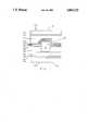
- FIG. 1is a cross sectional view of a bonding site formed by means of the present invention.
- the present inventionis a method for cold bonding of two surfaces. It is envisioned that the method will have numerous and varied applications.
- FIG. 1illustrates the bond formed by the method of the present invention.
- the individual dies 12In the IC fabrication process, the individual dies 12 must be bonded to a support package 14. The dies 12 are bonded to the package 14 via the dies 12 contacting a bond pad 16 formed on the package 14.
- the preferred embodiment of the present inventionis a new method to achieve the die/package interconnect bond 10.
- the die 12is prepared by applying metal layers to a die substrate 18 through photolithographic or material addition processes. To begin, a first bonding layer 20, selected for malleability and conductivity, is applied. To the first bonding layer 20 a first aluminum layer 24 is applied. The die 12 is then ready for bonding.
- the bond pad 16is also constructed of layers deposited upon a pad substrate 26. Similar to the die 12 preparation, the bond pad 16 has a second bonding layer 28 (similar to the first bonding layer 20), a first barrier metal layer 30, and a low resistance trace layer 32, all applied to the pad substrate 28, in the order stated. However, the bond pad 16 requires further preparation.
- the next step in preparation of the pad 16 in the preferred embodimentis to deposit a metal layer 34 with particles 36 reverse transfer molded therein onto the trace layer 32 of the pad 16.
- Reverse transfer moldingis a well known, commercially available process. Other processes, such as plating, can also be used to secure the particles 36 in position.
- the particles 36are covered by a particle bonding layer 38, then by a particle barrier layer 40.
- the result at this pointis that the bond pad 16 has particles 36 secured in and protruding from the metal layer 34.
- the location of the particles 36, and the extent to which they protrude from the metal layer 34,is determined by the topography of the die 12. That is, the particles 36 are photomasked into place to correspond with the contour of the die 12.
- the pad 16may be further prepared by applying a breakaway layer 42.
- the purpose of the breakaway layer 42is to define the point at which the bond 10 can be most easily broken. Accordingly, the force and amount of heat required to break the bond can be altered by varying the material used for the breakaway layer 42.
- the die 12When bonding is to occur, the die 12 is brought into physical contact with the package 14. This causes the metalized particles 48 protruding from the bond pad 16 to contact the appropriate connection site on the die 12. When essentially perpendicular force is applied, the metalized particles 48 displace any oxide present on the aluminum layers 24 and 46 so that two surfaces of virgin aluminum contact each other.
- the two aluminum layers 24 and 46form a metal matrix, thus creating a bond 10.
- the strength of the bondis dependent on the extent of formation of the metal matrix, which is a function of the amount of virgin aluminum that has been exposed. Therefore, the strength of the bond 10 formed can be controlled by the depth of the penetration of the metalized particles 48. For a temporary testing bond, the penetration is slight. If the tests prove positive, the penetration is simply increased by addition of further pressure, and a more permanent bond is formed.
- the materials chosen for the various components of the die 12 and bond pad 16can be varied to control the electrical and thermal conductivity properties of the bond 10. It is further understood that specific materials can be varied widely, while still following the teachings of this invention. However, in the preferred embodiment, a die/package interconnect bond 10, the materials are as set forth below.
- the die substrate 18is silcon. To this the thin first bonding layer 20 of platinum alloy is applied. This layer is covered by the first aluminum layer 24, whose thickness and contour are determined by the specific application.
- the pad substrate 26is usually alumina, beryllium oxide, or polyamide, and may sometimes be silicon as well. Thinly applied to this are the second bonding layer 28 of nickel/chrome and the first barrier metal layer 30 of nickel. Next is the low resistance trace layer 32, which in this embodiment is gold. Then, the third nickel/chrome bonding layer 38 and the nickel particle barrier layer 40 are applied. This provides a suitable surface to apply the breakaway layer 42.
- the material for the breakaway layer 42is chosen so that this layer is where the bond 10 can be most easily broken through the application of heat and force. In this embodiment, the breakaway layer 42 is gold/tin alloy. To provide better adhesion of the second aluminum layer 46, a barrier layer 44 of nickel is applied to the breakaway layer 42.
- the particles 36will usually be industrial diamond. Note that recent material technology advances provide diamond that is electrically conductive. It should also be noted that the size of the particles 36 can vary greatly. In this embodiment for IC's, the size of the particles 36 limits the obtainable density. The fact that the particles 36 can be as small as one micron is what allows for the density increase relative to the prior art bonding technologies. In other applications of the present invention, the particles 36 may be orders of magnitude larger. For example, large chunks may be used in an application where it is desired to bond metal plates together.
- the present inventionwill be used in applications where it is required that the particles 36 be both thermally and electrically insulating.
- the particles 36will be alumina, quartz, borosilicate, or the like.
- the cold bonding method of the present inventionhas enormous potential for industrial application.
- wafer sorting through final package testentails five distinct operations.
- the variable bond strength feature of the present inventionallows those steps to be combined into one operation.
- the present inventionallows a temporary bond, sufficiently strong for testing purposes, to be formed. If the die tests as good, additional pressure can be applied so that the bond is made permanent. If the die is bad, it is easily replaced.
- the permanent nature of the bondsdemanded that extensive rework be performed to replace a bad die. (The alternative being disposal of a part that had already had value added.) A conservative estimate is that processing time can be reduced by 25%. This application alone will make the present invention of tremendous utility in the IC industry.
- Wafer probe fabricationcan now be automated, through the use of a photomask (pad master).
- Hybrid circuitscan be more efficiently tested, as the present invention will allow the final hybrid configuration to be more closely simulated prior to bonding and during mass termination of multiple dies during bonding.
- the present technologywill allow for wafer scale testing.
- the method of the present inventionallows for the burn-in probe to be on a material that will not become flexible when heated, e.g. silicon or borasilicate glass.
- the geometry of the present inventiondue to the ability to easily control the particle size, allows for much greater circuit density.
- a 2 micron pad sizeis potentially feasible, as compared to the industry norm of pad size, which is 150-160 microns. This factor clearly pushes back one of the limits currently restricting circuit density.
- the present inventionwill greatly enhance IC manufacturing. Given the characteristics of the IC market, such improvement will be eagerly accepted. Further, the present invention has various additional applications as described above. Therefore, it is expected that the present invention will enjoy widespread commercial viability and industrial utility.
Landscapes
- Engineering & Computer Science (AREA)
- Computer Hardware Design (AREA)
- Microelectronics & Electronic Packaging (AREA)
- Power Engineering (AREA)
- Mechanical Engineering (AREA)
- Wire Bonding (AREA)
Abstract
Description
Claims (18)
Priority Applications (1)
| Application Number | Priority Date | Filing Date | Title |
|---|---|---|---|
| US07/090,608US4804132A (en) | 1987-08-28 | 1987-08-28 | Method for cold bonding |
Applications Claiming Priority (1)
| Application Number | Priority Date | Filing Date | Title |
|---|---|---|---|
| US07/090,608US4804132A (en) | 1987-08-28 | 1987-08-28 | Method for cold bonding |
Publications (1)
| Publication Number | Publication Date |
|---|---|
| US4804132Atrue US4804132A (en) | 1989-02-14 |
Family
ID=22223524
Family Applications (1)
| Application Number | Title | Priority Date | Filing Date |
|---|---|---|---|
| US07/090,608Expired - LifetimeUS4804132A (en) | 1987-08-28 | 1987-08-28 | Method for cold bonding |
Country Status (1)
| Country | Link |
|---|---|
| US (1) | US4804132A (en) |
Cited By (115)
| Publication number | Priority date | Publication date | Assignee | Title |
|---|---|---|---|---|
| EP0388933A3 (en)* | 1989-03-23 | 1991-07-31 | Hughes Aircraft Company | Alloy bonded indium bumps and methods of processing same |
| WO1991012108A1 (en)* | 1990-02-14 | 1991-08-22 | Bahl, Kenneth, S. | Particle-enhanced joining of metal surfaces |
| US5102336A (en)* | 1988-09-30 | 1992-04-07 | Linkow Leonard I | Neckless blade implant |
| US5110293A (en)* | 1988-09-30 | 1992-05-05 | Linkow Leonard I | Neckless blade implant |
| US5170930A (en)* | 1991-11-14 | 1992-12-15 | Microelectronics And Computer Technology Corporation | Liquid metal paste for thermal and electrical connections |
| US5267867A (en)* | 1992-09-11 | 1993-12-07 | Digital Equipment Corporation | Package for multiple removable integrated circuits |
| US5316863A (en)* | 1992-05-18 | 1994-05-31 | Alcan International Limited | Self-brazing aluminum laminated structure |
| US5328087A (en)* | 1993-03-29 | 1994-07-12 | Microelectronics And Computer Technology Corporation | Thermally and electrically conductive adhesive material and method of bonding with same |
| US5402077A (en)* | 1992-11-20 | 1995-03-28 | Micromodule Systems, Inc. | Bare die carrier |
| US5428298A (en)* | 1991-07-18 | 1995-06-27 | Gold Star Electron Co., Ltd. | Probe structure for testing a semiconductor chip and a press member for same |
| US5445308A (en)* | 1993-03-29 | 1995-08-29 | Nelson; Richard D. | Thermally conductive connection with matrix material and randomly dispersed filler containing liquid metal |
| US5456404A (en)* | 1993-10-28 | 1995-10-10 | Digital Equipment Corporation | Method of testing semiconductor chips with reusable test package |
| US5600099A (en)* | 1994-12-02 | 1997-02-04 | Augat Inc. | Chemically grafted electrical devices |
| US5623213A (en)* | 1994-09-09 | 1997-04-22 | Micromodule Systems | Membrane probing of circuits |
| US5812925A (en)* | 1996-10-23 | 1998-09-22 | Ecer; Gunes M. | Low temperature bonding of materials |
| US5829988A (en)* | 1996-11-14 | 1998-11-03 | Amkor Electronics, Inc. | Socket assembly for integrated circuit chip carrier package |
| US5847571A (en)* | 1994-09-09 | 1998-12-08 | Micromodule Systems | Membrane probing of circuits |
| US5876580A (en)* | 1996-01-12 | 1999-03-02 | Micromodule Systems | Rough electrical contact surface |
| US5880591A (en)* | 1996-04-16 | 1999-03-09 | Teradyne, Inc. | System for circuit modules having a plurality of independently positionable probes |
| US5929521A (en)* | 1997-03-26 | 1999-07-27 | Micron Technology, Inc. | Projected contact structure for bumped semiconductor device and resulting articles and assemblies |
| US5949029A (en)* | 1994-08-23 | 1999-09-07 | Thomas & Betts International, Inc. | Conductive elastomers and methods for fabricating the same |
| US5973504A (en)* | 1994-10-28 | 1999-10-26 | Kulicke & Soffa Industries, Inc. | Programmable high-density electronic device testing |
| US6284108B1 (en) | 1998-08-31 | 2001-09-04 | Louis DiFrancesco | Method and apparatus for momentum plating |
| US6326704B1 (en) | 1995-06-07 | 2001-12-04 | Automotive Technologies International Inc. | Vehicle electrical system |
| US6533316B2 (en) | 1995-06-07 | 2003-03-18 | Automotive Technologies International, Inc. | Automotive electronic safety network |
| US6557747B2 (en)* | 1998-01-12 | 2003-05-06 | The Furukawa Electric Co., Ltd. | Highly gas tight chamber and method of manufacturing same |
| US6630203B2 (en) | 2001-06-15 | 2003-10-07 | Nanopierce Technologies, Inc. | Electroless process for the preparation of particle enhanced electric contact surfaces |
| US6648367B2 (en) | 1995-06-07 | 2003-11-18 | Automotive Technologies International Inc. | Integrated occupant protection system |
| US20040087128A1 (en)* | 2000-10-24 | 2004-05-06 | Neuhaus Herbert J | Method and materials for printing particle-enhanced electrical contacts |
| US6733036B2 (en) | 1995-06-07 | 2004-05-11 | Automotive Technologies International, Inc. | Automotive electronic safety network |
| US20050116326A1 (en)* | 2003-10-06 | 2005-06-02 | Tessera, Inc. | Formation of circuitry with modification of feature height |
| US20050173805A1 (en)* | 2003-12-30 | 2005-08-11 | Tessera, Inc. | Micro pin grid array with pin motion isolation |
| US20050181544A1 (en)* | 2003-12-30 | 2005-08-18 | Tessera, Inc. | Microelectronic packages and methods therefor |
| US20050181655A1 (en)* | 2003-12-30 | 2005-08-18 | Tessera, Inc. | Micro pin grid array with wiping action |
| US6937044B1 (en) | 1992-11-20 | 2005-08-30 | Kulicke & Soffa Industries, Inc. | Bare die carrier |
| US20050285246A1 (en)* | 2004-06-25 | 2005-12-29 | Tessera, Inc. | Microelectronic packages and methods therefor |
| US20050284658A1 (en)* | 2003-10-06 | 2005-12-29 | Tessera, Inc. | Components with posts and pads |
| US20060115323A1 (en)* | 2004-11-04 | 2006-06-01 | Coppeta Jonathan R | Compression and cold weld sealing methods and devices |
| US20060133198A1 (en)* | 2004-12-03 | 2006-06-22 | Fisher Rayette A | Large area transducer array |
| US20060249857A1 (en)* | 2005-03-16 | 2006-11-09 | Tessera, Inc. | Microelectronic packages and methods therefor |
| US20070148822A1 (en)* | 2005-12-23 | 2007-06-28 | Tessera, Inc. | Microelectronic packages and methods therefor |
| US20070148819A1 (en)* | 2005-12-23 | 2007-06-28 | Tessera, Inc. | Microelectronic assemblies having very fine pitch stacking |
| US20080003402A1 (en)* | 2003-10-06 | 2008-01-03 | Tessera, Inc. | Fine pitch microcontacts and method for forming thereof |
| US20080042250A1 (en)* | 2006-08-18 | 2008-02-21 | Tessera, Inc. | Stacked microelectronic assemblies and methods therefor |
| US20080111024A1 (en)* | 2006-11-10 | 2008-05-15 | Lee Shin S | Composite Aircraft Structures With Hat Stiffeners |
| US20080140278A1 (en)* | 1995-06-07 | 2008-06-12 | Automotive Technologies International, Inc. | Vehicle Software Upgrade Techniques |
| US20080150101A1 (en)* | 2006-12-20 | 2008-06-26 | Tessera, Inc. | Microelectronic packages having improved input/output connections and methods therefor |
| US20090104736A1 (en)* | 2004-11-03 | 2009-04-23 | Tessera, Inc. | Stacked Packaging Improvements |
| US20090200655A1 (en)* | 1994-12-29 | 2009-08-13 | Tessera, Inc. | Method of electrically connecting a microelectronic component |
| US20100044860A1 (en)* | 2008-08-21 | 2010-02-25 | Tessera Interconnect Materials, Inc. | Microelectronic substrate or element having conductive pads and metal posts joined thereto using bond layer |
| US8330272B2 (en) | 2010-07-08 | 2012-12-11 | Tessera, Inc. | Microelectronic packages with dual or multiple-etched flip-chip connectors |
| US8404520B1 (en) | 2011-10-17 | 2013-03-26 | Invensas Corporation | Package-on-package assembly with wire bond vias |
| US8482111B2 (en) | 2010-07-19 | 2013-07-09 | Tessera, Inc. | Stackable molded microelectronic packages |
| US8580607B2 (en) | 2010-07-27 | 2013-11-12 | Tessera, Inc. | Microelectronic packages with nanoparticle joining |
| US20130325323A1 (en) | 1998-10-22 | 2013-12-05 | American Vehicular Sciences | Vehicle software upgrade techniques |
| US8623706B2 (en) | 2010-11-15 | 2014-01-07 | Tessera, Inc. | Microelectronic package with terminals on dielectric mass |
| US8835228B2 (en) | 2012-05-22 | 2014-09-16 | Invensas Corporation | Substrate-less stackable package with wire-bond interconnect |
| US8853558B2 (en) | 2010-12-10 | 2014-10-07 | Tessera, Inc. | Interconnect structure |
| US8872318B2 (en) | 2011-08-24 | 2014-10-28 | Tessera, Inc. | Through interposer wire bond using low CTE interposer with coarse slot apertures |
| US8878353B2 (en) | 2012-12-20 | 2014-11-04 | Invensas Corporation | Structure for microelectronic packaging with bond elements to encapsulation surface |
| US8883563B1 (en) | 2013-07-15 | 2014-11-11 | Invensas Corporation | Fabrication of microelectronic assemblies having stack terminals coupled by connectors extending through encapsulation |
| US8884448B2 (en) | 2007-09-28 | 2014-11-11 | Tessera, Inc. | Flip chip interconnection with double post |
| US8975738B2 (en) | 2012-11-12 | 2015-03-10 | Invensas Corporation | Structure for microelectronic packaging with terminals on dielectric mass |
| US9022417B2 (en) | 1995-12-12 | 2015-05-05 | American Vehicular Sciences Llc | Single side curtain airbag for vehicles |
| US9023691B2 (en) | 2013-07-15 | 2015-05-05 | Invensas Corporation | Microelectronic assemblies with stack terminals coupled by connectors extending through encapsulation |
| US9034696B2 (en) | 2013-07-15 | 2015-05-19 | Invensas Corporation | Microelectronic assemblies having reinforcing collars on connectors extending through encapsulation |
| US9082753B2 (en) | 2013-11-12 | 2015-07-14 | Invensas Corporation | Severing bond wire by kinking and twisting |
| US9087815B2 (en) | 2013-11-12 | 2015-07-21 | Invensas Corporation | Off substrate kinking of bond wire |
| US9093435B2 (en) | 2011-05-03 | 2015-07-28 | Tessera, Inc. | Package-on-package assembly with wire bonds to encapsulation surface |
| US9137903B2 (en) | 2010-12-21 | 2015-09-15 | Tessera, Inc. | Semiconductor chip assembly and method for making same |
| US9159708B2 (en) | 2010-07-19 | 2015-10-13 | Tessera, Inc. | Stackable molded microelectronic packages with area array unit connectors |
| US9214454B2 (en) | 2014-03-31 | 2015-12-15 | Invensas Corporation | Batch process fabrication of package-on-package microelectronic assemblies |
| US9224717B2 (en) | 2011-05-03 | 2015-12-29 | Tessera, Inc. | Package-on-package assembly with wire bonds to encapsulation surface |
| US9324681B2 (en) | 2010-12-13 | 2016-04-26 | Tessera, Inc. | Pin attachment |
| US9349706B2 (en) | 2012-02-24 | 2016-05-24 | Invensas Corporation | Method for package-on-package assembly with wire bonds to encapsulation surface |
| US9391008B2 (en) | 2012-07-31 | 2016-07-12 | Invensas Corporation | Reconstituted wafer-level package DRAM |
| US9412714B2 (en) | 2014-05-30 | 2016-08-09 | Invensas Corporation | Wire bond support structure and microelectronic package including wire bonds therefrom |
| US9435855B2 (en) | 2013-11-19 | 2016-09-06 | Teradyne, Inc. | Interconnect for transmitting signals between a device and a tester |
| US9502390B2 (en) | 2012-08-03 | 2016-11-22 | Invensas Corporation | BVA interposer |
| US9583411B2 (en) | 2014-01-17 | 2017-02-28 | Invensas Corporation | Fine pitch BVA using reconstituted wafer with area array accessible for testing |
| US9594114B2 (en) | 2014-06-26 | 2017-03-14 | Teradyne, Inc. | Structure for transmitting signals in an application space between a device under test and test electronics |
| US9601454B2 (en) | 2013-02-01 | 2017-03-21 | Invensas Corporation | Method of forming a component having wire bonds and a stiffening layer |
| US9633971B2 (en) | 2015-07-10 | 2017-04-25 | Invensas Corporation | Structures and methods for low temperature bonding using nanoparticles |
| US9646917B2 (en) | 2014-05-29 | 2017-05-09 | Invensas Corporation | Low CTE component with wire bond interconnects |
| US9659848B1 (en) | 2015-11-18 | 2017-05-23 | Invensas Corporation | Stiffened wires for offset BVA |
| US9685365B2 (en) | 2013-08-08 | 2017-06-20 | Invensas Corporation | Method of forming a wire bond having a free end |
| US9691679B2 (en) | 2012-02-24 | 2017-06-27 | Invensas Corporation | Method for package-on-package assembly with wire bonds to encapsulation surface |
| US9728527B2 (en) | 2013-11-22 | 2017-08-08 | Invensas Corporation | Multiple bond via arrays of different wire heights on a same substrate |
| US9735084B2 (en) | 2014-12-11 | 2017-08-15 | Invensas Corporation | Bond via array for thermal conductivity |
| US9761554B2 (en) | 2015-05-07 | 2017-09-12 | Invensas Corporation | Ball bonding metal wire bond wires to metal pads |
| US9812402B2 (en) | 2015-10-12 | 2017-11-07 | Invensas Corporation | Wire bond wires for interference shielding |
| US9842745B2 (en) | 2012-02-17 | 2017-12-12 | Invensas Corporation | Heat spreading substrate with embedded interconnects |
| US9852969B2 (en) | 2013-11-22 | 2017-12-26 | Invensas Corporation | Die stacks with one or more bond via arrays of wire bond wires and with one or more arrays of bump interconnects |
| US9888579B2 (en) | 2015-03-05 | 2018-02-06 | Invensas Corporation | Pressing of wire bond wire tips to provide bent-over tips |
| US9911718B2 (en) | 2015-11-17 | 2018-03-06 | Invensas Corporation | ‘RDL-First’ packaged microelectronic device for a package-on-package device |
| US9935075B2 (en) | 2016-07-29 | 2018-04-03 | Invensas Corporation | Wire bonding method and apparatus for electromagnetic interference shielding |
| US9977052B2 (en) | 2016-10-04 | 2018-05-22 | Teradyne, Inc. | Test fixture |
| US9984992B2 (en) | 2015-12-30 | 2018-05-29 | Invensas Corporation | Embedded wire bond wires for vertical integration with separate surface mount and wire bond mounting surfaces |
| US10008469B2 (en) | 2015-04-30 | 2018-06-26 | Invensas Corporation | Wafer-level packaging using wire bond wires in place of a redistribution layer |
| US10008477B2 (en) | 2013-09-16 | 2018-06-26 | Invensas Corporation | Microelectronic element with bond elements to encapsulation surface |
| US10026717B2 (en) | 2013-11-22 | 2018-07-17 | Invensas Corporation | Multiple bond via arrays of different wire heights on a same substrate |
| US10181457B2 (en) | 2015-10-26 | 2019-01-15 | Invensas Corporation | Microelectronic package for wafer-level chip scale packaging with fan-out |
| US10299368B2 (en) | 2016-12-21 | 2019-05-21 | Invensas Corporation | Surface integrated waveguides and circuit structures therefor |
| US10332854B2 (en) | 2015-10-23 | 2019-06-25 | Invensas Corporation | Anchoring structure of fine pitch bva |
| US10381326B2 (en) | 2014-05-28 | 2019-08-13 | Invensas Corporation | Structure and method for integrated circuits packaging with increased density |
| US10460958B2 (en) | 2013-08-07 | 2019-10-29 | Invensas Corporation | Method of manufacturing embedded packaging with preformed vias |
| US10490528B2 (en) | 2015-10-12 | 2019-11-26 | Invensas Corporation | Embedded wire bond wires |
| US10535626B2 (en) | 2015-07-10 | 2020-01-14 | Invensas Corporation | Structures and methods for low temperature bonding using nanoparticles |
| US10677815B2 (en) | 2018-06-08 | 2020-06-09 | Teradyne, Inc. | Test system having distributed resources |
| US11363746B2 (en) | 2019-09-06 | 2022-06-14 | Teradyne, Inc. | EMI shielding for a signal trace |
| CN116727825A (en)* | 2023-07-31 | 2023-09-12 | 河南科技大学 | A method of connecting dissimilar metals |
| US11862901B2 (en) | 2020-12-15 | 2024-01-02 | Teradyne, Inc. | Interposer |
| US11973056B2 (en) | 2016-10-27 | 2024-04-30 | Adeia Semiconductor Technologies Llc | Methods for low temperature bonding using nanoparticles |
| US12211809B2 (en) | 2020-12-30 | 2025-01-28 | Adeia Semiconductor Bonding Technologies Inc. | Structure with conductive feature and method of forming same |
| US12317757B2 (en) | 2018-10-11 | 2025-05-27 | SeeQC, Inc. | System and method for superconducting multi-chip module |
Citations (6)
| Publication number | Priority date | Publication date | Assignee | Title |
|---|---|---|---|---|
| US3100933A (en)* | 1956-10-15 | 1963-08-20 | Gen Motors Corp | Method of cold welding aluminum |
| US3203083A (en)* | 1961-02-08 | 1965-08-31 | Texas Instruments Inc | Method of manufacturing a hermetically sealed semiconductor capsule |
| US3482726A (en)* | 1967-02-13 | 1969-12-09 | Arthur Henry Schroeder Jr | Pressure weld seal for a composite glass body and method of forming said seal |
| US3555664A (en)* | 1967-04-29 | 1971-01-19 | Int Computers & Tabulators Ltd | Bonding electrical conductors |
| US3921885A (en)* | 1973-06-28 | 1975-11-25 | Rca Corp | Method of bonding two bodies together |
| GB2158757A (en)* | 1984-05-14 | 1985-11-20 | Pal Gal | Hot press welding process |
- 1987
- 1987-08-28USUS07/090,608patent/US4804132A/ennot_activeExpired - Lifetime
Patent Citations (6)
| Publication number | Priority date | Publication date | Assignee | Title |
|---|---|---|---|---|
| US3100933A (en)* | 1956-10-15 | 1963-08-20 | Gen Motors Corp | Method of cold welding aluminum |
| US3203083A (en)* | 1961-02-08 | 1965-08-31 | Texas Instruments Inc | Method of manufacturing a hermetically sealed semiconductor capsule |
| US3482726A (en)* | 1967-02-13 | 1969-12-09 | Arthur Henry Schroeder Jr | Pressure weld seal for a composite glass body and method of forming said seal |
| US3555664A (en)* | 1967-04-29 | 1971-01-19 | Int Computers & Tabulators Ltd | Bonding electrical conductors |
| US3921885A (en)* | 1973-06-28 | 1975-11-25 | Rca Corp | Method of bonding two bodies together |
| GB2158757A (en)* | 1984-05-14 | 1985-11-20 | Pal Gal | Hot press welding process |
Cited By (239)
| Publication number | Priority date | Publication date | Assignee | Title |
|---|---|---|---|---|
| US5102336A (en)* | 1988-09-30 | 1992-04-07 | Linkow Leonard I | Neckless blade implant |
| US5110293A (en)* | 1988-09-30 | 1992-05-05 | Linkow Leonard I | Neckless blade implant |
| EP0388933A3 (en)* | 1989-03-23 | 1991-07-31 | Hughes Aircraft Company | Alloy bonded indium bumps and methods of processing same |
| WO1991012108A1 (en)* | 1990-02-14 | 1991-08-22 | Bahl, Kenneth, S. | Particle-enhanced joining of metal surfaces |
| US5083697A (en)* | 1990-02-14 | 1992-01-28 | Difrancesco Louis | Particle-enhanced joining of metal surfaces |
| US5835359A (en)* | 1990-02-14 | 1998-11-10 | Particle Interconnect Corporation | Electrical interconnect using particle enhanced joining of metal surfaces |
| US5634265A (en)* | 1990-02-14 | 1997-06-03 | Particle Interconnect Corporation | Electrical interconnect using particle enhanced joining of metal surfaces |
| US5565280A (en)* | 1990-02-14 | 1996-10-15 | Particle Interconnect, Inc. | Electrical interconnect using particle enhanced joining of metal surfaces |
| US5334809A (en)* | 1990-02-14 | 1994-08-02 | Particle Interconnect, Inc. | Particle enhanced joining of metal surfaces |
| US5506514A (en)* | 1990-02-14 | 1996-04-09 | Particle Interconnect, Inc. | Electrical interconnect using particle enhanced joining of metal surfaces |
| US5428298A (en)* | 1991-07-18 | 1995-06-27 | Gold Star Electron Co., Ltd. | Probe structure for testing a semiconductor chip and a press member for same |
| US5170930A (en)* | 1991-11-14 | 1992-12-15 | Microelectronics And Computer Technology Corporation | Liquid metal paste for thermal and electrical connections |
| US5316863A (en)* | 1992-05-18 | 1994-05-31 | Alcan International Limited | Self-brazing aluminum laminated structure |
| US5267867A (en)* | 1992-09-11 | 1993-12-07 | Digital Equipment Corporation | Package for multiple removable integrated circuits |
| US5402077A (en)* | 1992-11-20 | 1995-03-28 | Micromodule Systems, Inc. | Bare die carrier |
| US6937044B1 (en) | 1992-11-20 | 2005-08-30 | Kulicke & Soffa Industries, Inc. | Bare die carrier |
| US5445308A (en)* | 1993-03-29 | 1995-08-29 | Nelson; Richard D. | Thermally conductive connection with matrix material and randomly dispersed filler containing liquid metal |
| US5328087A (en)* | 1993-03-29 | 1994-07-12 | Microelectronics And Computer Technology Corporation | Thermally and electrically conductive adhesive material and method of bonding with same |
| US5456404A (en)* | 1993-10-28 | 1995-10-10 | Digital Equipment Corporation | Method of testing semiconductor chips with reusable test package |
| US5949029A (en)* | 1994-08-23 | 1999-09-07 | Thomas & Betts International, Inc. | Conductive elastomers and methods for fabricating the same |
| US5841291A (en)* | 1994-09-09 | 1998-11-24 | Micromodule Systems | Exchangeable membrane probe testing of circuits |
| US5847571A (en)* | 1994-09-09 | 1998-12-08 | Micromodule Systems | Membrane probing of circuits |
| US5623213A (en)* | 1994-09-09 | 1997-04-22 | Micromodule Systems | Membrane probing of circuits |
| US5973504A (en)* | 1994-10-28 | 1999-10-26 | Kulicke & Soffa Industries, Inc. | Programmable high-density electronic device testing |
| US5600099A (en)* | 1994-12-02 | 1997-02-04 | Augat Inc. | Chemically grafted electrical devices |
| US20110017704A1 (en)* | 1994-12-29 | 2011-01-27 | Tessera, Inc. | Method of electrically connecting a microelectronic component |
| US8513799B2 (en) | 1994-12-29 | 2013-08-20 | Tessera, Inc. | Method of electrically connecting a microelectronic component |
| US8148199B2 (en) | 1994-12-29 | 2012-04-03 | Tessera, Inc. | Method of electrically connecting a microelectronic component |
| US20090200655A1 (en)* | 1994-12-29 | 2009-08-13 | Tessera, Inc. | Method of electrically connecting a microelectronic component |
| US8148205B2 (en) | 1994-12-29 | 2012-04-03 | Tessera, Inc. | Method of electrically connecting a microelectronic component |
| US20090200654A1 (en)* | 1994-12-29 | 2009-08-13 | Tessera, Inc. | Method of electrically connecting a microelectronic component |
| US20090236406A1 (en)* | 1994-12-29 | 2009-09-24 | Tessera, Inc. | Method of electrically connecting a microelectronic component |
| US8114711B2 (en) | 1994-12-29 | 2012-02-14 | Tessera, Inc. | Method of electrically connecting a microelectronic component |
| US6533316B2 (en) | 1995-06-07 | 2003-03-18 | Automotive Technologies International, Inc. | Automotive electronic safety network |
| US20080140278A1 (en)* | 1995-06-07 | 2008-06-12 | Automotive Technologies International, Inc. | Vehicle Software Upgrade Techniques |
| US6326704B1 (en) | 1995-06-07 | 2001-12-04 | Automotive Technologies International Inc. | Vehicle electrical system |
| US6648367B2 (en) | 1995-06-07 | 2003-11-18 | Automotive Technologies International Inc. | Integrated occupant protection system |
| US6733036B2 (en) | 1995-06-07 | 2004-05-11 | Automotive Technologies International, Inc. | Automotive electronic safety network |
| US9443358B2 (en) | 1995-06-07 | 2016-09-13 | Automotive Vehicular Sciences LLC | Vehicle software upgrade techniques |
| US9022417B2 (en) | 1995-12-12 | 2015-05-05 | American Vehicular Sciences Llc | Single side curtain airbag for vehicles |
| US6245445B1 (en) | 1996-01-12 | 2001-06-12 | Kulicke & Soffa Industries, Inc. | Rough electrical contact surface |
| US5876580A (en)* | 1996-01-12 | 1999-03-02 | Micromodule Systems | Rough electrical contact surface |
| US5880591A (en)* | 1996-04-16 | 1999-03-09 | Teradyne, Inc. | System for circuit modules having a plurality of independently positionable probes |
| US5812925A (en)* | 1996-10-23 | 1998-09-22 | Ecer; Gunes M. | Low temperature bonding of materials |
| US5829988A (en)* | 1996-11-14 | 1998-11-03 | Amkor Electronics, Inc. | Socket assembly for integrated circuit chip carrier package |
| US6613662B2 (en) | 1997-03-26 | 2003-09-02 | Micron Technology, Inc. | Method for making projected contact structures for engaging bumped semiconductor devices |
| US20070132097A1 (en)* | 1997-03-26 | 2007-06-14 | Wark James M | Projected contact structures for engaging bumped semiconductor devices |
| US20060055034A1 (en)* | 1997-03-26 | 2006-03-16 | Wark James M | Projected contact structures for engaging bumped semiconductor devices and methods of making the same |
| US20060060968A1 (en)* | 1997-03-26 | 2006-03-23 | Wark James M | Projected contact structures for engaging bumped semiconductor devices and methods of making the same |
| US5929521A (en)* | 1997-03-26 | 1999-07-27 | Micron Technology, Inc. | Projected contact structure for bumped semiconductor device and resulting articles and assemblies |
| US7115495B2 (en) | 1997-03-26 | 2006-10-03 | Micron Technology, Inc. | Methods of making projected contact structures for engaging bumped semiconductor devices |
| US6291897B1 (en) | 1997-03-26 | 2001-09-18 | Micron Technology, Inc. | Carriers including projected contact structures for engaging bumped semiconductor devices |
| US7161250B2 (en) | 1997-03-26 | 2007-01-09 | Micron Technology, Inc. | Projected contact structures for engaging bumped semiconductor devices and methods of making the same |
| US7205661B2 (en) | 1997-03-26 | 2007-04-17 | Micron Technology, Inc. | Projected contact structures for engaging bumped semiconductor devices and methods of making the same |
| US6557747B2 (en)* | 1998-01-12 | 2003-05-06 | The Furukawa Electric Co., Ltd. | Highly gas tight chamber and method of manufacturing same |
| US6284108B1 (en) | 1998-08-31 | 2001-09-04 | Louis DiFrancesco | Method and apparatus for momentum plating |
| US20130325323A1 (en) | 1998-10-22 | 2013-12-05 | American Vehicular Sciences | Vehicle software upgrade techniques |
| US10240935B2 (en) | 1998-10-22 | 2019-03-26 | American Vehicular Sciences Llc | Vehicle software upgrade techniques |
| US20040087128A1 (en)* | 2000-10-24 | 2004-05-06 | Neuhaus Herbert J | Method and materials for printing particle-enhanced electrical contacts |
| US6630203B2 (en) | 2001-06-15 | 2003-10-07 | Nanopierce Technologies, Inc. | Electroless process for the preparation of particle enhanced electric contact surfaces |
| US7816251B2 (en) | 2003-10-06 | 2010-10-19 | Tessera, Inc. | Formation of circuitry with modification of feature height |
| US8046912B2 (en) | 2003-10-06 | 2011-11-01 | Tessera, Inc. | Method of making a connection component with posts and pads |
| US20090133254A1 (en)* | 2003-10-06 | 2009-05-28 | Tessera, Inc. | Components with posts and pads |
| US20050116326A1 (en)* | 2003-10-06 | 2005-06-02 | Tessera, Inc. | Formation of circuitry with modification of feature height |
| US20080003402A1 (en)* | 2003-10-06 | 2008-01-03 | Tessera, Inc. | Fine pitch microcontacts and method for forming thereof |
| US20050284658A1 (en)* | 2003-10-06 | 2005-12-29 | Tessera, Inc. | Components with posts and pads |
| US8604348B2 (en) | 2003-10-06 | 2013-12-10 | Tessera, Inc. | Method of making a connection component with posts and pads |
| US8641913B2 (en) | 2003-10-06 | 2014-02-04 | Tessera, Inc. | Fine pitch microcontacts and method for forming thereof |
| US7462936B2 (en) | 2003-10-06 | 2008-12-09 | Tessera, Inc. | Formation of circuitry with modification of feature height |
| US7495179B2 (en) | 2003-10-06 | 2009-02-24 | Tessera, Inc. | Components with posts and pads |
| US7554206B2 (en) | 2003-12-30 | 2009-06-30 | Tessera, Inc. | Microelectronic packages and methods therefor |
| US20100193970A1 (en)* | 2003-12-30 | 2010-08-05 | Tessera, Inc. | Micro pin grid array with pin motion isolation |
| US20050173805A1 (en)* | 2003-12-30 | 2005-08-11 | Tessera, Inc. | Micro pin grid array with pin motion isolation |
| US7176043B2 (en) | 2003-12-30 | 2007-02-13 | Tessera, Inc. | Microelectronic packages and methods therefor |
| US20050181655A1 (en)* | 2003-12-30 | 2005-08-18 | Tessera, Inc. | Micro pin grid array with wiping action |
| US8207604B2 (en) | 2003-12-30 | 2012-06-26 | Tessera, Inc. | Microelectronic package comprising offset conductive posts on compliant layer |
| US8531039B2 (en) | 2003-12-30 | 2013-09-10 | Tessera, Inc. | Micro pin grid array with pin motion isolation |
| US20050181544A1 (en)* | 2003-12-30 | 2005-08-18 | Tessera, Inc. | Microelectronic packages and methods therefor |
| US7709968B2 (en) | 2003-12-30 | 2010-05-04 | Tessera, Inc. | Micro pin grid array with pin motion isolation |
| US7453157B2 (en) | 2004-06-25 | 2008-11-18 | Tessera, Inc. | Microelectronic packages and methods therefor |
| US7745943B2 (en) | 2004-06-25 | 2010-06-29 | Tessera, Inc. | Microelectonic packages and methods therefor |
| US20070205496A1 (en)* | 2004-06-25 | 2007-09-06 | Tessera, Inc. | Microelectronic packages and methods therefor |
| US20100258956A1 (en)* | 2004-06-25 | 2010-10-14 | Tessera, Inc. | Microelectronic packages and methods therefor |
| US20050285246A1 (en)* | 2004-06-25 | 2005-12-29 | Tessera, Inc. | Microelectronic packages and methods therefor |
| US7999397B2 (en) | 2004-06-25 | 2011-08-16 | Tessera, Inc. | Microelectronic packages and methods therefor |
| US8329581B2 (en) | 2004-06-25 | 2012-12-11 | Tessera, Inc. | Microelectronic packages and methods therefor |
| US8927337B2 (en) | 2004-11-03 | 2015-01-06 | Tessera, Inc. | Stacked packaging improvements |
| US8531020B2 (en) | 2004-11-03 | 2013-09-10 | Tessera, Inc. | Stacked packaging improvements |
| US8525314B2 (en) | 2004-11-03 | 2013-09-03 | Tessera, Inc. | Stacked packaging improvements |
| US20090104736A1 (en)* | 2004-11-03 | 2009-04-23 | Tessera, Inc. | Stacked Packaging Improvements |
| US20110042810A1 (en)* | 2004-11-03 | 2011-02-24 | Tessera, Inc. | Stacked packaging improvements |
| US9153562B2 (en) | 2004-11-03 | 2015-10-06 | Tessera, Inc. | Stacked packaging improvements |
| US9570416B2 (en) | 2004-11-03 | 2017-02-14 | Tessera, Inc. | Stacked packaging improvements |
| US20060115323A1 (en)* | 2004-11-04 | 2006-06-01 | Coppeta Jonathan R | Compression and cold weld sealing methods and devices |
| US8191756B2 (en)* | 2004-11-04 | 2012-06-05 | Microchips, Inc. | Hermetically sealing using a cold welded tongue and groove structure |
| US9796583B2 (en) | 2004-11-04 | 2017-10-24 | Microchips Biotech, Inc. | Compression and cold weld sealing method for an electrical via connection |
| US7867824B2 (en) | 2004-12-03 | 2011-01-11 | General Electric Company | Methods of fabricating a large area transducer array |
| US20060133198A1 (en)* | 2004-12-03 | 2006-06-22 | Fisher Rayette A | Large area transducer array |
| US20080213933A1 (en)* | 2004-12-03 | 2008-09-04 | General Electric Company | Methods of fabricating a large area transducer array |
| US7375420B2 (en) | 2004-12-03 | 2008-05-20 | General Electric Company | Large area transducer array |
| US20060249857A1 (en)* | 2005-03-16 | 2006-11-09 | Tessera, Inc. | Microelectronic packages and methods therefor |
| US7939934B2 (en) | 2005-03-16 | 2011-05-10 | Tessera, Inc. | Microelectronic packages and methods therefor |
| US20110165733A1 (en)* | 2005-12-23 | 2011-07-07 | Tessera, Inc. | Microelectronic packages and methods therefor |
| US8058101B2 (en) | 2005-12-23 | 2011-11-15 | Tessera, Inc. | Microelectronic packages and methods therefor |
| US9984901B2 (en) | 2005-12-23 | 2018-05-29 | Tessera, Inc. | Method for making a microelectronic assembly having conductive elements |
| US20100232129A1 (en)* | 2005-12-23 | 2010-09-16 | Tessera, Inc. | Microelectronic packages and methods therefor |
| US20070148822A1 (en)* | 2005-12-23 | 2007-06-28 | Tessera, Inc. | Microelectronic packages and methods therefor |
| US20070148819A1 (en)* | 2005-12-23 | 2007-06-28 | Tessera, Inc. | Microelectronic assemblies having very fine pitch stacking |
| US8728865B2 (en) | 2005-12-23 | 2014-05-20 | Tessera, Inc. | Microelectronic packages and methods therefor |
| US8093697B2 (en) | 2005-12-23 | 2012-01-10 | Tessera, Inc. | Microelectronic packages and methods therefor |
| US8067267B2 (en) | 2005-12-23 | 2011-11-29 | Tessera, Inc. | Microelectronic assemblies having very fine pitch stacking |
| US9218988B2 (en) | 2005-12-23 | 2015-12-22 | Tessera, Inc. | Microelectronic packages and methods therefor |
| US20080042250A1 (en)* | 2006-08-18 | 2008-02-21 | Tessera, Inc. | Stacked microelectronic assemblies and methods therefor |
| US7545029B2 (en) | 2006-08-18 | 2009-06-09 | Tessera, Inc. | Stack microelectronic assemblies |
| US7871040B2 (en)* | 2006-11-10 | 2011-01-18 | The Boeing Company | Composite aircraft structures with hat stiffeners |
| US20080111024A1 (en)* | 2006-11-10 | 2008-05-15 | Lee Shin S | Composite Aircraft Structures With Hat Stiffeners |
| US20080150101A1 (en)* | 2006-12-20 | 2008-06-26 | Tessera, Inc. | Microelectronic packages having improved input/output connections and methods therefor |
| US8884448B2 (en) | 2007-09-28 | 2014-11-11 | Tessera, Inc. | Flip chip interconnection with double post |
| US20100044860A1 (en)* | 2008-08-21 | 2010-02-25 | Tessera Interconnect Materials, Inc. | Microelectronic substrate or element having conductive pads and metal posts joined thereto using bond layer |
| US8330272B2 (en) | 2010-07-08 | 2012-12-11 | Tessera, Inc. | Microelectronic packages with dual or multiple-etched flip-chip connectors |
| US8723318B2 (en) | 2010-07-08 | 2014-05-13 | Tessera, Inc. | Microelectronic packages with dual or multiple-etched flip-chip connectors |
| US9123664B2 (en) | 2010-07-19 | 2015-09-01 | Tessera, Inc. | Stackable molded microelectronic packages |
| US9553076B2 (en) | 2010-07-19 | 2017-01-24 | Tessera, Inc. | Stackable molded microelectronic packages with area array unit connectors |
| US8907466B2 (en) | 2010-07-19 | 2014-12-09 | Tessera, Inc. | Stackable molded microelectronic packages |
| US10128216B2 (en) | 2010-07-19 | 2018-11-13 | Tessera, Inc. | Stackable molded microelectronic packages |
| US9159708B2 (en) | 2010-07-19 | 2015-10-13 | Tessera, Inc. | Stackable molded microelectronic packages with area array unit connectors |
| US9570382B2 (en) | 2010-07-19 | 2017-02-14 | Tessera, Inc. | Stackable molded microelectronic packages |
| US8482111B2 (en) | 2010-07-19 | 2013-07-09 | Tessera, Inc. | Stackable molded microelectronic packages |
| US9397063B2 (en) | 2010-07-27 | 2016-07-19 | Tessera, Inc. | Microelectronic packages with nanoparticle joining |
| US8580607B2 (en) | 2010-07-27 | 2013-11-12 | Tessera, Inc. | Microelectronic packages with nanoparticle joining |
| US9030001B2 (en) | 2010-07-27 | 2015-05-12 | Tessera, Inc. | Microelectronic packages with nanoparticle joining |
| US8659164B2 (en) | 2010-11-15 | 2014-02-25 | Tessera, Inc. | Microelectronic package with terminals on dielectric mass |
| US8637991B2 (en) | 2010-11-15 | 2014-01-28 | Tessera, Inc. | Microelectronic package with terminals on dielectric mass |
| US8623706B2 (en) | 2010-11-15 | 2014-01-07 | Tessera, Inc. | Microelectronic package with terminals on dielectric mass |
| US8957527B2 (en) | 2010-11-15 | 2015-02-17 | Tessera, Inc. | Microelectronic package with terminals on dielectric mass |
| US8853558B2 (en) | 2010-12-10 | 2014-10-07 | Tessera, Inc. | Interconnect structure |
| US9496236B2 (en) | 2010-12-10 | 2016-11-15 | Tessera, Inc. | Interconnect structure |
| US9324681B2 (en) | 2010-12-13 | 2016-04-26 | Tessera, Inc. | Pin attachment |
| US9137903B2 (en) | 2010-12-21 | 2015-09-15 | Tessera, Inc. | Semiconductor chip assembly and method for making same |
| US9716075B2 (en) | 2010-12-21 | 2017-07-25 | Tessera, Inc. | Semiconductor chip assembly and method for making same |
| US10062661B2 (en) | 2011-05-03 | 2018-08-28 | Tessera, Inc. | Package-on-package assembly with wire bonds to encapsulation surface |
| US9093435B2 (en) | 2011-05-03 | 2015-07-28 | Tessera, Inc. | Package-on-package assembly with wire bonds to encapsulation surface |
| US10593643B2 (en) | 2011-05-03 | 2020-03-17 | Tessera, Inc. | Package-on-package assembly with wire bonds to encapsulation surface |
| US9691731B2 (en) | 2011-05-03 | 2017-06-27 | Tessera, Inc. | Package-on-package assembly with wire bonds to encapsulation surface |
| US9224717B2 (en) | 2011-05-03 | 2015-12-29 | Tessera, Inc. | Package-on-package assembly with wire bonds to encapsulation surface |
| US11424211B2 (en) | 2011-05-03 | 2022-08-23 | Tessera Llc | Package-on-package assembly with wire bonds to encapsulation surface |
| US8872318B2 (en) | 2011-08-24 | 2014-10-28 | Tessera, Inc. | Through interposer wire bond using low CTE interposer with coarse slot apertures |
| US8836136B2 (en) | 2011-10-17 | 2014-09-16 | Invensas Corporation | Package-on-package assembly with wire bond vias |
| US10756049B2 (en) | 2011-10-17 | 2020-08-25 | Invensas Corporation | Package-on-package assembly with wire bond vias |
| US9761558B2 (en) | 2011-10-17 | 2017-09-12 | Invensas Corporation | Package-on-package assembly with wire bond vias |
| US9041227B2 (en) | 2011-10-17 | 2015-05-26 | Invensas Corporation | Package-on-package assembly with wire bond vias |
| US9252122B2 (en) | 2011-10-17 | 2016-02-02 | Invensas Corporation | Package-on-package assembly with wire bond vias |
| US11735563B2 (en) | 2011-10-17 | 2023-08-22 | Invensas Llc | Package-on-package assembly with wire bond vias |
| US8404520B1 (en) | 2011-10-17 | 2013-03-26 | Invensas Corporation | Package-on-package assembly with wire bond vias |
| US9105483B2 (en) | 2011-10-17 | 2015-08-11 | Invensas Corporation | Package-on-package assembly with wire bond vias |
| US11189595B2 (en) | 2011-10-17 | 2021-11-30 | Invensas Corporation | Package-on-package assembly with wire bond vias |
| US9842745B2 (en) | 2012-02-17 | 2017-12-12 | Invensas Corporation | Heat spreading substrate with embedded interconnects |
| US9349706B2 (en) | 2012-02-24 | 2016-05-24 | Invensas Corporation | Method for package-on-package assembly with wire bonds to encapsulation surface |
| US9691679B2 (en) | 2012-02-24 | 2017-06-27 | Invensas Corporation | Method for package-on-package assembly with wire bonds to encapsulation surface |
| US10510659B2 (en) | 2012-05-22 | 2019-12-17 | Invensas Corporation | Substrate-less stackable package with wire-bond interconnect |
| US8835228B2 (en) | 2012-05-22 | 2014-09-16 | Invensas Corporation | Substrate-less stackable package with wire-bond interconnect |
| US9953914B2 (en) | 2012-05-22 | 2018-04-24 | Invensas Corporation | Substrate-less stackable package with wire-bond interconnect |
| US10170412B2 (en) | 2012-05-22 | 2019-01-01 | Invensas Corporation | Substrate-less stackable package with wire-bond interconnect |
| US9917073B2 (en) | 2012-07-31 | 2018-03-13 | Invensas Corporation | Reconstituted wafer-level package dram with conductive interconnects formed in encapsulant at periphery of the package |
| US9391008B2 (en) | 2012-07-31 | 2016-07-12 | Invensas Corporation | Reconstituted wafer-level package DRAM |
| US9502390B2 (en) | 2012-08-03 | 2016-11-22 | Invensas Corporation | BVA interposer |
| US10297582B2 (en) | 2012-08-03 | 2019-05-21 | Invensas Corporation | BVA interposer |
| US8975738B2 (en) | 2012-11-12 | 2015-03-10 | Invensas Corporation | Structure for microelectronic packaging with terminals on dielectric mass |
| US9615456B2 (en) | 2012-12-20 | 2017-04-04 | Invensas Corporation | Microelectronic assembly for microelectronic packaging with bond elements to encapsulation surface |
| US9095074B2 (en) | 2012-12-20 | 2015-07-28 | Invensas Corporation | Structure for microelectronic packaging with bond elements to encapsulation surface |
| US8878353B2 (en) | 2012-12-20 | 2014-11-04 | Invensas Corporation | Structure for microelectronic packaging with bond elements to encapsulation surface |
| US9601454B2 (en) | 2013-02-01 | 2017-03-21 | Invensas Corporation | Method of forming a component having wire bonds and a stiffening layer |
| US9034696B2 (en) | 2013-07-15 | 2015-05-19 | Invensas Corporation | Microelectronic assemblies having reinforcing collars on connectors extending through encapsulation |
| US8883563B1 (en) | 2013-07-15 | 2014-11-11 | Invensas Corporation | Fabrication of microelectronic assemblies having stack terminals coupled by connectors extending through encapsulation |
| US9023691B2 (en) | 2013-07-15 | 2015-05-05 | Invensas Corporation | Microelectronic assemblies with stack terminals coupled by connectors extending through encapsulation |
| US9633979B2 (en) | 2013-07-15 | 2017-04-25 | Invensas Corporation | Microelectronic assemblies having stack terminals coupled by connectors extending through encapsulation |
| US10460958B2 (en) | 2013-08-07 | 2019-10-29 | Invensas Corporation | Method of manufacturing embedded packaging with preformed vias |
| US9685365B2 (en) | 2013-08-08 | 2017-06-20 | Invensas Corporation | Method of forming a wire bond having a free end |
| US10008477B2 (en) | 2013-09-16 | 2018-06-26 | Invensas Corporation | Microelectronic element with bond elements to encapsulation surface |
| US9893033B2 (en) | 2013-11-12 | 2018-02-13 | Invensas Corporation | Off substrate kinking of bond wire |
| US9087815B2 (en) | 2013-11-12 | 2015-07-21 | Invensas Corporation | Off substrate kinking of bond wire |
| US9082753B2 (en) | 2013-11-12 | 2015-07-14 | Invensas Corporation | Severing bond wire by kinking and twisting |
| US9435855B2 (en) | 2013-11-19 | 2016-09-06 | Teradyne, Inc. | Interconnect for transmitting signals between a device and a tester |
| USRE49987E1 (en) | 2013-11-22 | 2024-05-28 | Invensas Llc | Multiple plated via arrays of different wire heights on a same substrate |
| US9852969B2 (en) | 2013-11-22 | 2017-12-26 | Invensas Corporation | Die stacks with one or more bond via arrays of wire bond wires and with one or more arrays of bump interconnects |
| US9728527B2 (en) | 2013-11-22 | 2017-08-08 | Invensas Corporation | Multiple bond via arrays of different wire heights on a same substrate |
| US10290613B2 (en) | 2013-11-22 | 2019-05-14 | Invensas Corporation | Multiple bond via arrays of different wire heights on a same substrate |
| US10026717B2 (en) | 2013-11-22 | 2018-07-17 | Invensas Corporation | Multiple bond via arrays of different wire heights on a same substrate |
| US10629567B2 (en) | 2013-11-22 | 2020-04-21 | Invensas Corporation | Multiple plated via arrays of different wire heights on same substrate |
| US11404338B2 (en) | 2014-01-17 | 2022-08-02 | Invensas Corporation | Fine pitch bva using reconstituted wafer with area array accessible for testing |
| US9583411B2 (en) | 2014-01-17 | 2017-02-28 | Invensas Corporation | Fine pitch BVA using reconstituted wafer with area array accessible for testing |
| US9837330B2 (en) | 2014-01-17 | 2017-12-05 | Invensas Corporation | Fine pitch BVA using reconstituted wafer with area array accessible for testing |
| US11990382B2 (en) | 2014-01-17 | 2024-05-21 | Adeia Semiconductor Technologies Llc | Fine pitch BVA using reconstituted wafer with area array accessible for testing |
| US10529636B2 (en) | 2014-01-17 | 2020-01-07 | Invensas Corporation | Fine pitch BVA using reconstituted wafer with area array accessible for testing |
| US9214454B2 (en) | 2014-03-31 | 2015-12-15 | Invensas Corporation | Batch process fabrication of package-on-package microelectronic assemblies |
| US9356006B2 (en) | 2014-03-31 | 2016-05-31 | Invensas Corporation | Batch process fabrication of package-on-package microelectronic assemblies |
| US9812433B2 (en) | 2014-03-31 | 2017-11-07 | Invensas Corporation | Batch process fabrication of package-on-package microelectronic assemblies |
| US10381326B2 (en) | 2014-05-28 | 2019-08-13 | Invensas Corporation | Structure and method for integrated circuits packaging with increased density |
| US10032647B2 (en) | 2014-05-29 | 2018-07-24 | Invensas Corporation | Low CTE component with wire bond interconnects |
| US10475726B2 (en) | 2014-05-29 | 2019-11-12 | Invensas Corporation | Low CTE component with wire bond interconnects |
| US9646917B2 (en) | 2014-05-29 | 2017-05-09 | Invensas Corporation | Low CTE component with wire bond interconnects |
| US9947641B2 (en) | 2014-05-30 | 2018-04-17 | Invensas Corporation | Wire bond support structure and microelectronic package including wire bonds therefrom |
| US9412714B2 (en) | 2014-05-30 | 2016-08-09 | Invensas Corporation | Wire bond support structure and microelectronic package including wire bonds therefrom |
| US9594114B2 (en) | 2014-06-26 | 2017-03-14 | Teradyne, Inc. | Structure for transmitting signals in an application space between a device under test and test electronics |
| US9735084B2 (en) | 2014-12-11 | 2017-08-15 | Invensas Corporation | Bond via array for thermal conductivity |
| US9888579B2 (en) | 2015-03-05 | 2018-02-06 | Invensas Corporation | Pressing of wire bond wire tips to provide bent-over tips |
| US10806036B2 (en) | 2015-03-05 | 2020-10-13 | Invensas Corporation | Pressing of wire bond wire tips to provide bent-over tips |
| US10008469B2 (en) | 2015-04-30 | 2018-06-26 | Invensas Corporation | Wafer-level packaging using wire bond wires in place of a redistribution layer |
| US9761554B2 (en) | 2015-05-07 | 2017-09-12 | Invensas Corporation | Ball bonding metal wire bond wires to metal pads |
| US11710718B2 (en) | 2015-07-10 | 2023-07-25 | Adeia Semiconductor Technologies Llc | Structures and methods for low temperature bonding using nanoparticles |
| US10886250B2 (en) | 2015-07-10 | 2021-01-05 | Invensas Corporation | Structures and methods for low temperature bonding using nanoparticles |
| US10535626B2 (en) | 2015-07-10 | 2020-01-14 | Invensas Corporation | Structures and methods for low temperature bonding using nanoparticles |
| US9818713B2 (en) | 2015-07-10 | 2017-11-14 | Invensas Corporation | Structures and methods for low temperature bonding using nanoparticles |
| US10892246B2 (en) | 2015-07-10 | 2021-01-12 | Invensas Corporation | Structures and methods for low temperature bonding using nanoparticles |
| US9633971B2 (en) | 2015-07-10 | 2017-04-25 | Invensas Corporation | Structures and methods for low temperature bonding using nanoparticles |
| US10490528B2 (en) | 2015-10-12 | 2019-11-26 | Invensas Corporation | Embedded wire bond wires |
| US10115678B2 (en) | 2015-10-12 | 2018-10-30 | Invensas Corporation | Wire bond wires for interference shielding |
| US10559537B2 (en) | 2015-10-12 | 2020-02-11 | Invensas Corporation | Wire bond wires for interference shielding |
| US9812402B2 (en) | 2015-10-12 | 2017-11-07 | Invensas Corporation | Wire bond wires for interference shielding |
| US11462483B2 (en) | 2015-10-12 | 2022-10-04 | Invensas Llc | Wire bond wires for interference shielding |
| US10332854B2 (en) | 2015-10-23 | 2019-06-25 | Invensas Corporation | Anchoring structure of fine pitch bva |
| US10181457B2 (en) | 2015-10-26 | 2019-01-15 | Invensas Corporation | Microelectronic package for wafer-level chip scale packaging with fan-out |
| US10043779B2 (en) | 2015-11-17 | 2018-08-07 | Invensas Corporation | Packaged microelectronic device for a package-on-package device |
| US9911718B2 (en) | 2015-11-17 | 2018-03-06 | Invensas Corporation | ‘RDL-First’ packaged microelectronic device for a package-on-package device |
| US9659848B1 (en) | 2015-11-18 | 2017-05-23 | Invensas Corporation | Stiffened wires for offset BVA |
| US9984992B2 (en) | 2015-12-30 | 2018-05-29 | Invensas Corporation | Embedded wire bond wires for vertical integration with separate surface mount and wire bond mounting surfaces |
| US10325877B2 (en) | 2015-12-30 | 2019-06-18 | Invensas Corporation | Embedded wire bond wires for vertical integration with separate surface mount and wire bond mounting surfaces |
| US10658302B2 (en) | 2016-07-29 | 2020-05-19 | Invensas Corporation | Wire bonding method and apparatus for electromagnetic interference shielding |
| US9935075B2 (en) | 2016-07-29 | 2018-04-03 | Invensas Corporation | Wire bonding method and apparatus for electromagnetic interference shielding |
| US9977052B2 (en) | 2016-10-04 | 2018-05-22 | Teradyne, Inc. | Test fixture |
| US11973056B2 (en) | 2016-10-27 | 2024-04-30 | Adeia Semiconductor Technologies Llc | Methods for low temperature bonding using nanoparticles |
| US12027487B2 (en) | 2016-10-27 | 2024-07-02 | Adeia Semiconductor Technologies Llc | Structures for low temperature bonding using nanoparticles |
| US10299368B2 (en) | 2016-12-21 | 2019-05-21 | Invensas Corporation | Surface integrated waveguides and circuit structures therefor |
| US10677815B2 (en) | 2018-06-08 | 2020-06-09 | Teradyne, Inc. | Test system having distributed resources |
| US12317757B2 (en) | 2018-10-11 | 2025-05-27 | SeeQC, Inc. | System and method for superconducting multi-chip module |
| US11363746B2 (en) | 2019-09-06 | 2022-06-14 | Teradyne, Inc. | EMI shielding for a signal trace |
| US11862901B2 (en) | 2020-12-15 | 2024-01-02 | Teradyne, Inc. | Interposer |
| US12211809B2 (en) | 2020-12-30 | 2025-01-28 | Adeia Semiconductor Bonding Technologies Inc. | Structure with conductive feature and method of forming same |
| CN116727825A (en)* | 2023-07-31 | 2023-09-12 | 河南科技大学 | A method of connecting dissimilar metals |
Similar Documents
| Publication | Publication Date | Title |
|---|---|---|
| US4804132A (en) | Method for cold bonding | |
| US5083697A (en) | Particle-enhanced joining of metal surfaces | |
| Kristiansen et al. | Overview of conductive adhesive interconnection technologies for LCDs | |
| JPH11510649A (en) | Deformable substrate assembly for adhesive bonded electronic devices | |
| US5971253A (en) | Microelectronic component mounting with deformable shell terminals | |
| US4930001A (en) | Alloy bonded indium bumps and methods of processing same | |
| US5749997A (en) | Composite bump tape automated bonding method and bonded structure | |
| US6199751B1 (en) | Polymer with transient liquid phase bondable particles | |
| JPH09312176A (en) | Connecting member, and structure and method for connecting electrodes using this connecting member | |
| JPH04366630A (en) | Anisotropic conductive adhesive tape | |
| Aschenbrenner et al. | Flip chip attachment using anisotropic conductive adhesives and electroless nickel bumps | |
| US5693574A (en) | Process for the laminar joining of silicon semiconductor slices | |
| JP3052074B2 (en) | Burn-in test substrate for integrated circuit chip and method for manufacturing know good die using the same | |
| JP2001513265A (en) | How to connect components and arrangements | |
| US20040154165A1 (en) | Method for manufacturing a probe pin and a probe card | |
| EP0539211B1 (en) | Method for production of microcapsule type conductive filler | |
| Jeng et al. | Application of Al/PI composite bumps to COG bonding process | |
| Shi et al. | A novel high performance die attach for ceramic packages | |
| Schubert et al. | Do chip size limits exist for DCA? | |
| US20020102765A1 (en) | Forming an electrical contact on an electronic component | |
| JPH06275678A (en) | Connecting between chip and substrate using conductive bonding agent improved in repair property | |
| Chaitra et al. | Study on the effect of substrate material on the mechanical strength of Cu bonds bonded through flip chip bonding | |
| JPS61181136A (en) | Die bonding | |
| JPS62115748A (en) | Formation of gold bump | |
| JPH06203640A (en) | Anisotropic electric conductive bonding agent and electric conductive connection structure |
Legal Events
| Date | Code | Title | Description |
|---|---|---|---|
| STCF | Information on status: patent grant | Free format text:PATENTED CASE | |
| FEPP | Fee payment procedure | Free format text:PAT HLDR NO LONGER CLAIMS SMALL ENT STAT AS SMALL BUSINESS (ORIGINAL EVENT CODE: LSM2); ENTITY STATUS OF PATENT OWNER: SMALL ENTITY Free format text:PAYOR NUMBER ASSIGNED (ORIGINAL EVENT CODE: ASPN); ENTITY STATUS OF PATENT OWNER: SMALL ENTITY | |
| FPAY | Fee payment | Year of fee payment:4 | |
| AS | Assignment | Owner name:PARTICLE INTERCONNECT, INC., CALIFORNIA Free format text:ASSIGNMENT OF ASSIGNORS INTEREST;ASSIGNOR:DIFRANCESCO, LOUIS;REEL/FRAME:007000/0923 Effective date:19940402 | |
| AS | Assignment | Owner name:MICROMODULE SYSTEMS INC., CALIFORNIA Free format text:EXCLUSIVE WORLDWIDE, IRREVOCABLE, NON-TRANSFERABLE LICENSE AGREEMENT.;ASSIGNOR:PI PARTNERSHIP;REEL/FRAME:007319/0065 Effective date:19930910 | |
| FEPP | Fee payment procedure | Free format text:PAT HOLDER CLAIMS SMALL ENTITY STATUS - SMALL BUSINESS (ORIGINAL EVENT CODE: SM02); ENTITY STATUS OF PATENT OWNER: SMALL ENTITY | |
| FEPP | Fee payment procedure | Free format text:PAYER NUMBER DE-ASSIGNED (ORIGINAL EVENT CODE: RMPN); ENTITY STATUS OF PATENT OWNER: SMALL ENTITY | |
| FPAY | Fee payment | Year of fee payment:8 | |
| AS | Assignment | Owner name:PARTICLE INTERCONNECT CORPORATION, COLORADO Free format text:ASSIGNMENT OF ASSIGNORS INTEREST;ASSIGNOR:PARTICLE INTERCONNECT, INC.;REEL/FRAME:008119/0861 Effective date:19960903 | |
| AS | Assignment | Owner name:NANOPIERCE TECHNOLOGIES, INC., COLORADO Free format text:ASSIGNMENT OF ASSIGNORS INTEREST;ASSIGNOR:PARTICLE INTERCONNECT CORPORATION;REEL/FRAME:009027/0538 Effective date:19980227 | |
| AS | Assignment | Owner name:EXATRON AUTOMATED TEST EQUIPMENT, INC., A CORP. OF Free format text:LICENSE;ASSIGNOR:DIFRANCESCO, LOUIS;REEL/FRAME:009257/0727 Effective date:19940331 | |
| FEPP | Fee payment procedure | Free format text:PAYOR NUMBER ASSIGNED (ORIGINAL EVENT CODE: ASPN); ENTITY STATUS OF PATENT OWNER: SMALL ENTITY | |
| FPAY | Fee payment | Year of fee payment:12 |