US4800486A - Multiple data patch CPU architecture - Google Patents
Multiple data patch CPU architectureDownload PDFInfo
- Publication number
- US4800486A US4800486AUS06/537,877US53787783AUS4800486AUS 4800486 AUS4800486 AUS 4800486AUS 53787783 AUS53787783 AUS 53787783AUS 4800486 AUS4800486 AUS 4800486A
- Authority
- US
- United States
- Prior art keywords
- register
- operands
- arithmetic logic
- microcode
- parity
- Prior art date
- Legal status (The legal status is an assumption and is not a legal conclusion. Google has not performed a legal analysis and makes no representation as to the accuracy of the status listed.)
- Expired - Lifetime
Links
Images


Classifications
- G—PHYSICS
- G06—COMPUTING OR CALCULATING; COUNTING
- G06F—ELECTRIC DIGITAL DATA PROCESSING
- G06F9/00—Arrangements for program control, e.g. control units
- G06F9/06—Arrangements for program control, e.g. control units using stored programs, i.e. using an internal store of processing equipment to receive or retain programs
- G06F9/30—Arrangements for executing machine instructions, e.g. instruction decode
- G06F9/38—Concurrent instruction execution, e.g. pipeline or look ahead
- G06F9/3885—Concurrent instruction execution, e.g. pipeline or look ahead using a plurality of independent parallel functional units
- G—PHYSICS
- G06—COMPUTING OR CALCULATING; COUNTING
- G06F—ELECTRIC DIGITAL DATA PROCESSING
- G06F15/00—Digital computers in general; Data processing equipment in general
- G06F15/16—Combinations of two or more digital computers each having at least an arithmetic unit, a program unit and a register, e.g. for a simultaneous processing of several programs
- G06F15/163—Interprocessor communication
- G—PHYSICS
- G06—COMPUTING OR CALCULATING; COUNTING
- G06F—ELECTRIC DIGITAL DATA PROCESSING
- G06F9/00—Arrangements for program control, e.g. control units
- G06F9/06—Arrangements for program control, e.g. control units using stored programs, i.e. using an internal store of processing equipment to receive or retain programs
- G06F9/30—Arrangements for executing machine instructions, e.g. instruction decode
- G06F9/38—Concurrent instruction execution, e.g. pipeline or look ahead
- G06F9/3885—Concurrent instruction execution, e.g. pipeline or look ahead using a plurality of independent parallel functional units
- G06F9/3893—Concurrent instruction execution, e.g. pipeline or look ahead using a plurality of independent parallel functional units controlled in tandem, e.g. multiplier-accumulator
- G06F9/3895—Concurrent instruction execution, e.g. pipeline or look ahead using a plurality of independent parallel functional units controlled in tandem, e.g. multiplier-accumulator for complex operations, e.g. multidimensional or interleaved address generators, macros
- G06F9/3897—Concurrent instruction execution, e.g. pipeline or look ahead using a plurality of independent parallel functional units controlled in tandem, e.g. multiplier-accumulator for complex operations, e.g. multidimensional or interleaved address generators, macros with adaptable data path
Definitions
- the present inventionrelates to the central processing unit (CPU) of a data processing system. More particularly, the present invention relates to the organization of the various functional units which comprise a CPU and enables a main arithmetic logic unit (ALU) and various special function units to access data registers, literal constants and data from a memory cache.
- CPUcentral processing unit
- ALUmain arithmetic logic unit
- the central processing unit (CPU) of a data processing systemis the portion of the system where data manipulation, logical and arithmetic operations and other data alteration take place.
- the physical and logical interconnection of the elements of the CPU, the arithmetic logic unit and various registers and multiplexers in a CPUis known as a data path.
- prior art CPU'smay or may not be arranged in a pipelined configuration, i.e., in two or more stages from a timing standpoint such that the execution of a single microinstruction line proceeds in several steps through the data path.
- Pipelined architectureenables a faster throughput of data through a CPU by allowing portions of different consecutive instructions to be executed simultaneously. For example, while a later phase or rank of a first instruction is being executed, an earlier phase or rank of a second instruction may also be executed.
- Prior art CPU's which are not organized in a pipelined mannerare generally not capable of the same instruction throughput rate which pipelined machines are capable.
- Another object of the present inventionis to provide a CPU data path architecture having multiple data paths.
- a further object of the present inventionis to provide a multiple data path CPU architecture which minimizes the multiporting of registers and the use of wide multiplexers.
- Another object of the present inventionis to provide a multiple data path CPU architecture which allows more than one operation to take place in the CPU per instruction cycle.
- a multiple data path CPUwherein data sources such as a multiple register file, a memory cache, literal constant register, ALU output and special function output register are organized into at least two sets of operand buses, one set feeding an ALU and one set feeding a set of special function units whose functions are microcode controlled.
- Each operand busis sourced by a multiplexer which draws from a subset of the possible data sources, including holding registers which store the results of the previous operations of the ALU and special function units.
- While prior art multiple data path schemesgenerally multiplex the data sources in a single stage using one or more large multiplexers, the present invention utilizes two stages in a pipelined arrangement where a first rank accomplishes the decoding of the multiple register file and a miscellaneous register multiplexer and a second rank addresses main multiplexers and controls ALU and special function unit functions. Control of special functions includes the selection of one of N special function units and the definition of its function.
- the special function arrangementis a closely coupled scheme wherein an auxiliary data path and a set of N special function units, each capable of executing a plurality of functions, interfaces with the main ALU data path.
- Virtually any special functionmay be implemented, i.e., an auxiliary ALU; access to a set of scratch-pad registers; barrel shifter; interface to other processors in a multiprocessor system via an interprocessor bus; interface to main memory; interrupt implementation; read and write access to writable control store; interval timer; I/O channel interface.
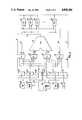
- FIG. 1is a block diagram of the CPU of the present invention.
- FIG. 2is a block diagram of an auxiliary ALU implemented as a special function.
- FIG. 3is a block diagram of a scratchpad register array implemented as a special function unit.
- FIG. 4is a block diagram of a special function parity generation hardware.
- FIG. 5is a block diagram of the conditional test hardware capabilities of the special function modules.
- FIG. 1the overall data path architecture block diagram is depicted.
- ALU 10 and special functions units 12a, 12b, 12c . . . 12nare serviced by the available data resources.
- the output of ALU 10is made available on main bus 14 and the outputs of the special function units 12 share (i.e., only a single one is enabled at a time) special main bus 16.
- the source data for these two data resourcesare delivered on two analogous sets of buses, main buses J and K, 18 and 20 respectively, sourced by 4:1 multiplexers 22 and 24 respectively, and special buses SJ and SK, 26 and 28 respectively, sourced by 4:1 multiplexers 30 and 32 respectively.
- Multiplexer selectionis made via microcode fields as is well understood by those of ordinary skill in the art. While in this preferred embodiment 4:1 multiplexers are used, those skilled in the art will readily observe that a system of richer input interconnection could be supplied, but at the expense of greater hardware complexity with the uncertain benefit of enhanced flexibility.
- the 4:1 multiplexers 22 and 30, sourcing the J bus 18 and SJ bus 26,are sourced by several sources; J register 34, CD register 36, M register 38 and SM register 40.
- the 4:1 multiplexers 24 and 32, sourcing the K bus 20 and SK bus 28,are sourced by M register 38, SM register 40, K register 42 and LIT register 44.
- the data pathis enriched by the commonality of data source registers M 38 and SM 40 to both the M and SM data paths through either side of ALU 10, via J register 34 and K register 42, and thus across J bus 18 and K bus 20, and also through either side of any of the special function modules 12a through 12n, via SJ 4:1 multiplexer 30 and SK 4:1 multiplexer 32, and through SJ bus 26 and SK bus 28.
- the M register 38holds the results of the previous main ALU result, delivered to its input from the output of ALU 10 via M bus 14.
- the SM register 40holds the data result of the previous selected special function from any one of special function modules 12a through 12n.
- the J register 34 and the K register 42each hold the contents of a selected one of a plurality of registers, principally including a selected one of the multiple register file 46.
- the register filemay be loaded from the M register 38.
- the J or the K registersmay take data from other registers, such as a program counter or memory address registers through other multiplexers as is known.
- the CD register 36holds the output contents of an addressable cache 48 which is loaded from SM register 40 via line 49.
- the last principal register in this rank of registersis the LIT register 44 which, as its name implies, holds a literal constant supplied by a microcode bit field 50.
- the multiple register file 46is controlled by several microcode fields which specify: the register, if any, to drive to J register 34, and K register 42; the register in the file to be loaded from the M register 38.
- a pointer register(not shown) acts in conjunction with microcode to select registers to be loaded and read. This register may be loaded from M bus 14 or incremented or decremented by use of microcode fields. All fields used to load these file registers are in rank two, all fields used to read them are in rank one.
- the operation of the data path in FIG. 1is preferably accomplished by means of at least a minimal two rank microcode pipeline such as that described in copending applications Ser. No. 537,429, abandoned, filed Sept. 29, 1983, and Ser. No. 537,038, U.S. Pat. No. 457,344, filed Sept. 29, 1983, assigned to the same assignee which are expressly incorporated herein by reference.
- the rank one microcode bit field of a given microinstructiondecodes the microcode addressing functions for the multiple register file 46, the multiplexer 52 which places the results of one of a number of miscellaneous registers into the input of J register 34, and multiplexer 54 which selects a source for data to the input of the K register 42.
- Multiplexers 52 and 54form ports to less frequently accessed registers, such as a program counter, memory address registers, or status registers. Those skilled in the art will recognize that this feature allows access to many registers while leaving the main register paths unencumbered.
- the rank two portion microcode bit field of any given microinstructiondecodes the 4:1 multiplexers 22, 24, 30 and 32 and controls and defines the operation of ALU 10 and special function units 12a through 12n. With respect to the special function units, a portion of the rank two microcode bit field controls both the selection of one of n special function units 12a through 12n, and also defines its function. Those skilled in the art will recognize that the particular portion of the available microcode field used is unimportant and that any bit positions in the appropriate rank of microcode field may be used. All registers are clocked simultaneously except that CD register 36 is clocked only when microcode specifies a load from the cache. A microcode field provides an inhibit signal (not shown) to CD register 36 to perform this inhibit function.
- Each special function unit 12a through 12nmay be dedicated to a related group of tasks.
- onemay be an auxiliary ALU capable of performing logical or arithmetic functions and returning the result to the SM bus.
- ALU unit 100has its input 102 connected to SJ bus 26 and input 104 connected to SK bus 28.
- ALU 100also has its output 106 connected to buffer 108.
- Buffer 108returns the ALU result to the SM bus 16. Since more than one special function unit is attached to the SM bus, buffer 108 has means to prevent bus contention by assuring that this special function unit has control of SM bus 16 only when it is selected. Accordingly, buffer 108 has an OE (output enable) input which is driven by decode unit 110.
- a microcode field 112 in rank twodrives decode unit 110 and drives similar decode units for all special function units attached to SM bus 16. Each decode unit is conditioned to recognize only one of all possible combinations of microcode appearing in microcode field 112. Thus, only one decode unit will enable a buffer to attach a special function unit to the SM 16.
- a second microcode field 114 in rank twois shown as an input to ALU unit 100.
- This microcode fielddefines the operation to be performed by ALU unit 100 as is known in the art.
- any special unitsuch as ALU unit 100
- ALU unit 100is always attached to the SJ and SK buses, thus always prepared to perform its function. Only one function, however, has control of the SM bus at any one time. This selection is determined by microcode field 112 and decoded by decoder 110 thus enabling buffer 108 to drive the SM bus 16 only when ALU 100 has been selected by a particular bit pattern in microcode field 112.
- This hardwareprovides a method for verifying the correct operation of various parts of the CPU which may not be protected by other means (such as parity) without large amounts of redundant circuitry. The checking proceeds concurrently with normal system operation without impacting performance.
- the simple ADD macroinstructiondoes not require the use of the special function modules 12a through 12n and may thus have a test function imbedded in unused lines of its microcode.
- the operands to be addedare presented to ALU 10 on J bus 18 and K bus 20.
- the same operandsmay be simultaneously presented to special function ALU 100.
- the following clockthe results of the main ALU and special ALU are available in M register 38 and SM register 40. These results may then be passed through multiplexers 30 and 32 and presented to inputs 102 and 104 of the special function ALU.
- the microcode field 114performs the check function which instructs special ALU 100 to perform a subtract and to halt the CPU if the result is nonzero as indicated by line 116. Thus, the correct operation of both ALU's as well as many of the control paths has been verified.
- Scratchpad 120which may be configured of RAM or other suitable memory or register devices, is shown connected to the SJ, SK and SM buses, 26, 28, and 16, respectively.
- the SJ busis used as a data input port for scratchpad 120
- the SK busis used to hold a portion of the address used to access scratchpad 120.
- Another portion of the address used to address scratchpad 120is derived from microcode field 114.
- a decode unit 122examines microcode field 112 to determine whether a particular bit pattern has selected scratchpad 120 for enabling on to SM bus 16.
- decode unit 122has two outputs. One of these outputs, line 124, provides a single bit to the output enable of scratchpad 120. This output enable input is used as is known in the art to disable the output drivers of scratchpad 120 so that it may selectively be connected to SM bus 16.
- the second output, line 126is used to drive read/write input of scratchpad 120 and defines whether scratchpad 120 will be performing a read or a write operation.
- microcode field 112is generally usable to decode the selection of a particular special function unit and place its output on SM bus 16.
- Microcode field 114is useful for performing special addressing functions or function definitions for whatever special function unit is embodied.
- parityWhile parity is normally sent along with the data it serves, the special function units 12a through 12n send parity a clock cycle later. Otherwise, in cases where a special function unit 12a through 12n would generate parity in series with output data from a special function unit, the generation of parity would slow down the cycle time of the machine.
- special function units 12a through 12nsend parity information a clock cycle later than data information.
- the parity generation timetherefore does not affect the minimum cycle time of the CPU.
- FIG. 4illustrates special function units 12a through 12n with their inputs connected to SJ bus 26, SK bus 28, and their outputs connected to SM bus 16.
- FIG. 4illustrates SJ parity bus 26a and SK parity bus 28a driving the inputs of both special function modules as well as SM parity bus 16a being selectively driven by special function units 12a through 12n.
- Special function unit 12aas illustrative of all special function units, is seen to contain parity pass or generate unit 202 as well as the special function operation 200, which may be, for instance, ALU 100 of FIG. 2, or scratchpad 120 of FIG. 3. Depending on the nature of the particular special function unit involved, parity for this unit may either be passed through or generated. For instance, if the special function unit is a scratchpad, parity is merely passed along with the data to be stored in the scratchpad. If special function operation 200 is an ALU, parity will be generated from the ALU result.
- Parity pass or generate unit 202can also employ these forms of parity prediction.
- the resulting parity bit generated by parity pass or generate unit 202is placed in SM parity bus delay register unit 204 on the first effective clock following its generation.
- microcode field 112which, as previously discussed is used to enable a particular special function unit 12a through 12n is shown driving the decode unit 206.
- Decode unit 206is similar in function to decode unit 110 and 122 from FIGS. 2 and 3, however it is shown here possessing another function relating to parity.
- a portion of the output of decode unit 206is shown performing the SM bus output function via buffer 208 which is shown schematically as one having a disable function as is known in the art.
- the output of decode unit 206also supplies the data input to SM parity drive delay register 210.
- the output of SM parity drive delay register 210drives the enable/disable line of output buffer 212 which delivers the SM parity bus delay register result to the SM parity bus 16a.
- parity bus 16adrives parity check 216.
- the output of SM register 214is delivered to parity checker 216 as is the unregistered parity bit from SM parity bus 16a. Since the parity bit on SM bus parity bus 16a has been delayed by one clock cycle, the addition of SM register 214 to the parity data bus delays the data output on the SM bus 16 by that one clock cycle so that parity checking unit 216 receives both data and the parity bit at the same time.
- parity bitsmay be used to cover various subfields of the entire word. Two parity bits, each covering one half (lower or upper) of a word might be used.
- FIG. 5a block diagram of the conditional test hardware capabilities of the special function modules, the hardware architecture allowing the CPU sequencer to branch on numerous test conditions will be disclosed.
- each of special function module units 12a through 12nare various special function units which are capable of performing various tests on the parameters with which they operate.
- the special function unitis an ALU
- Each special function unit 12is equipped with two multiplexers 130 and 132, respectively which select from among the numerous test conditions available for that module via a portion of microcode field 114, discussed previously with respect to FIGS. 2, 3 and 4.
- the outputs of multiplexers 130 and 132are driven on two buses, STESTA bus 134 and STESTB bus 136, respectively, via buffers 138 and 140, respectively. In a manner similar to that depicted in FIGS.
- buffers 138 and 140may have their outputs disabled when special unit function 12 with which they are associated is not driving either the SM bus or STESTA line 134 or STESTB line 136.
- the disabling inputs of buffers 138 and 140are driven by decode circuit 110 which decodes a microcode bit field 112 as previously discussed with respect to these special function units.
- sequencer branch hardware unit 139terminates in sequencer conditional branch hardware unit 139.
- the function of sequencer branch hardware unit 139is to use the tests results supplied to it by the STESTA and STESTB buses to perform microbranching and to selectively inhibit lines of microcode when certain microbranches have been taken.
- the architecture and functioning of sequencer conditional branch hardware unit 139is completely disclosed in copending applications Ser. No. 537,886, filed Sept. 29, 1983 now U.S. Pat. No. 4,571,673, assigned to the same assignee as the present invention, which is expressly incorporated herein by reference.
- widths of the particular buses shown hereinmay be determined with reference to a particular application. While the inventors have employed a width of 16 bits plus two parity bits, the actual bus widths which may be used with the current invention are simply a matter of design choice.
- registers, multiplexers, ALU's and special function logicmay be implemented as discrete logic elements or as part of gate arrays or custom LSI.
Landscapes
- Engineering & Computer Science (AREA)
- Theoretical Computer Science (AREA)
- Software Systems (AREA)
- Physics & Mathematics (AREA)
- General Engineering & Computer Science (AREA)
- General Physics & Mathematics (AREA)
- Computer Hardware Design (AREA)
- Executing Machine-Instructions (AREA)
- Multi Processors (AREA)
- Advance Control (AREA)
- Image Processing (AREA)
- Test And Diagnosis Of Digital Computers (AREA)
- Transition And Organic Metals Composition Catalysts For Addition Polymerization (AREA)
- Catalysts (AREA)
- Hardware Redundancy (AREA)
- Control By Computers (AREA)
- Memory System Of A Hierarchy Structure (AREA)
- Logic Circuits (AREA)
- Communication Control (AREA)
- Electrotherapy Devices (AREA)
- Dram (AREA)
Abstract
Description
Claims (15)
Priority Applications (19)
| Application Number | Priority Date | Filing Date | Title |
|---|---|---|---|
| US06/537,877US4800486A (en) | 1983-09-29 | 1983-09-29 | Multiple data patch CPU architecture |
| NZ209663ANZ209663A (en) | 1983-09-29 | 1984-09-24 | Dual data path cpu architecture |
| ZA847524AZA847524B (en) | 1983-09-29 | 1984-09-25 | Automatic memory board reconfiguration |
| FI843781AFI85428C (en) | 1983-09-29 | 1984-09-26 | Central unit architecture with many data routes |
| IL73106AIL73106A (en) | 1983-09-29 | 1984-09-26 | Multiple data path cpu architecture |
| AU33596/84AAU574387B2 (en) | 1983-09-29 | 1984-09-27 | Multiple data path cpu architecture |
| DE8484306591TDE3483669D1 (en) | 1983-09-29 | 1984-09-27 | CENTRAL PROCESSOR ARCHITECTURE WITH MULTIPLE DATA WAY. |
| IN694/CAL/84AIN162545B (en) | 1983-09-29 | 1984-09-27 | |
| EP84306591AEP0136179B1 (en) | 1983-09-29 | 1984-09-27 | Multiple data path cpu architecture |
| IE2461/84AIE56554B1 (en) | 1983-09-29 | 1984-09-27 | Multiple data path cpu architecture |
| DK462584ADK165202C (en) | 1983-09-29 | 1984-09-27 | CENTRAL PROCESSING UNIT WITH MULTIPLE DATA WAYS FOR A DATA PROCESSING PLANT |
| AT84306591TATE58794T1 (en) | 1983-09-29 | 1984-09-27 | CPU ARCHITECTURE WITH MULTIPLE DATA PATH. |
| KR1019840005995AKR920004059B1 (en) | 1983-09-29 | 1984-09-28 | Multiple Data Pathway Central Processing Unit Architecture |
| JP59203894AJPH0752386B2 (en) | 1983-09-29 | 1984-09-28 | Multi-data path CPU architecture |
| NO843891ANO168497C (en) | 1983-09-29 | 1984-09-28 | CENTRAL PROCESSING DEVICE IN DATA PROCESSING SYSTEMS WITH "PIPELINE" ARCHITECTURE. |
| MX202897AMX157907A (en) | 1983-09-29 | 1984-09-28 | IMPROVEMENTS IN DATA PROCESSING SYSTEM FOR A CENTRAL PROCESSING UNIT ORGANIZED TO ALLOW THE CHAINING OF PROCESSES AND THE OVERLAYING OF THE EXECUTION OF SEVERAL INSTRUCTIONS |
| BR8404918ABR8404918A (en) | 1983-09-29 | 1984-09-28 | CONFIGURATION OF CENTRAL PROCESSING UNIT WITH INFORMATION CHANNELS FOR USE IN DATA PROCESSING SYSTEMS |
| CA000464281ACA1215783A (en) | 1983-09-29 | 1984-09-28 | Multiple data path cpu architecture |
| HK461/91AHK46191A (en) | 1983-09-29 | 1991-06-11 | Multiple data path cpu architecture |
Applications Claiming Priority (1)
| Application Number | Priority Date | Filing Date | Title |
|---|---|---|---|
| US06/537,877US4800486A (en) | 1983-09-29 | 1983-09-29 | Multiple data patch CPU architecture |
Publications (1)
| Publication Number | Publication Date |
|---|---|
| US4800486Atrue US4800486A (en) | 1989-01-24 |
Family
ID=24144474
Family Applications (1)
| Application Number | Title | Priority Date | Filing Date |
|---|---|---|---|
| US06/537,877Expired - LifetimeUS4800486A (en) | 1983-09-29 | 1983-09-29 | Multiple data patch CPU architecture |
Country Status (19)
| Country | Link |
|---|---|
| US (1) | US4800486A (en) |
| EP (1) | EP0136179B1 (en) |
| JP (1) | JPH0752386B2 (en) |
| KR (1) | KR920004059B1 (en) |
| AT (1) | ATE58794T1 (en) |
| AU (1) | AU574387B2 (en) |
| BR (1) | BR8404918A (en) |
| CA (1) | CA1215783A (en) |
| DE (1) | DE3483669D1 (en) |
| DK (1) | DK165202C (en) |
| FI (1) | FI85428C (en) |
| HK (1) | HK46191A (en) |
| IE (1) | IE56554B1 (en) |
| IL (1) | IL73106A (en) |
| IN (1) | IN162545B (en) |
| MX (1) | MX157907A (en) |
| NO (1) | NO168497C (en) |
| NZ (1) | NZ209663A (en) |
| ZA (1) | ZA847524B (en) |
Cited By (12)
| Publication number | Priority date | Publication date | Assignee | Title |
|---|---|---|---|---|
| US4891754A (en)* | 1987-07-02 | 1990-01-02 | General Datacomm Inc. | Microinstruction sequencer for instructing arithmetic, logical and data move operations in a conditional manner |
| US5032986A (en)* | 1987-07-28 | 1991-07-16 | Texas Instruments Incorporated | Data processing device with parallel circular addressing hardware |
| US5109497A (en)* | 1989-01-27 | 1992-04-28 | Hughes Aircraft Company | Arithmetic element controller for controlling data, control and micro store memories |
| US5648733A (en)* | 1995-11-01 | 1997-07-15 | Lsi Logic Corporation | Scan compatible 3-state bus control |
| US20090070532A1 (en)* | 2007-09-11 | 2009-03-12 | Vinod Bussa | System and Method for Efficiently Testing Cache Congruence Classes During Processor Design Verification and Validation |
| US20090070631A1 (en)* | 2007-09-11 | 2009-03-12 | Sampan Arora | System and Method for Re-Shuffling Test Case Instruction Orders for Processor Design Verification and Validation |
| US20090070629A1 (en)* | 2007-09-11 | 2009-03-12 | Sampan Arora | System and Method for Testing Multiple Processor Modes for Processor Design Verification and Validation |
| US20090070546A1 (en)* | 2007-09-11 | 2009-03-12 | Shubhodeep Roy Choudhury | System and Method for Generating Fast Instruction and Data Interrupts for Processor Design Verification and Validation |
| US20090070570A1 (en)* | 2007-09-11 | 2009-03-12 | Shubhodeep Roy Choudhury | System and Method for Efficiently Handling Interrupts |
| US20100011248A1 (en)* | 2008-07-14 | 2010-01-14 | International Business Machines Corporation | Light weight and high throughput test case generation methodology for testing cache/tlb intervention and diagnostics |
| US7992059B2 (en) | 2007-09-11 | 2011-08-02 | International Business Machines Corporation | System and method for testing a large memory area during processor design verification and validation |
| US20140101383A1 (en)* | 2012-10-04 | 2014-04-10 | Texas Instruments Incorporated | Register bank cross path connection method in a multi core processor system |
Families Citing this family (9)
| Publication number | Priority date | Publication date | Assignee | Title |
|---|---|---|---|---|
| GB8401807D0 (en)* | 1984-01-24 | 1984-02-29 | Int Computers Ltd | Pipelined data processing apparatus |
| JPH01255031A (en)* | 1988-04-05 | 1989-10-11 | Matsushita Electric Ind Co Ltd | arithmetic processing unit |
| KR100294276B1 (en)* | 1991-07-08 | 2001-09-17 | 야스카와 히데아키 | RSC microprocessor structure with high speed trap and exception |
| US5961629A (en)* | 1991-07-08 | 1999-10-05 | Seiko Epson Corporation | High performance, superscalar-based computer system with out-of-order instruction execution |
| US5539911A (en)* | 1991-07-08 | 1996-07-23 | Seiko Epson Corporation | High-performance, superscalar-based computer system with out-of-order instruction execution |
| EP0547247B1 (en) | 1991-07-08 | 2001-04-04 | Seiko Epson Corporation | Extensible risc microprocessor architecture |
| US5438668A (en) | 1992-03-31 | 1995-08-01 | Seiko Epson Corporation | System and method for extraction, alignment and decoding of CISC instructions into a nano-instruction bucket for execution by a RISC computer |
| US6735685B1 (en) | 1992-09-29 | 2004-05-11 | Seiko Epson Corporation | System and method for handling load and/or store operations in a superscalar microprocessor |
| EP0663083B1 (en) | 1992-09-29 | 2000-12-20 | Seiko Epson Corporation | System and method for handling load and/or store operations in a superscalar microprocessor |
Citations (23)
| Publication number | Priority date | Publication date | Assignee | Title |
|---|---|---|---|---|
| US3886523A (en)* | 1973-06-05 | 1975-05-27 | Burroughs Corp | Micro program data processor having parallel instruction flow streams for plural levels of sub instruction sets |
| US3900723A (en)* | 1974-05-28 | 1975-08-19 | Control Data Corp | Apparatus for controlling computer pipelines for arithmetic operations on vectors |
| US4041461A (en)* | 1975-07-25 | 1977-08-09 | International Business Machines Corporation | Signal analyzer system |
| US4101960A (en)* | 1977-03-29 | 1978-07-18 | Burroughs Corporation | Scientific processor |
| US4112489A (en)* | 1976-02-06 | 1978-09-05 | International Computers Limited | Data processing systems |
| US4128880A (en)* | 1976-06-30 | 1978-12-05 | Cray Research, Inc. | Computer vector register processing |
| US4179734A (en)* | 1976-07-02 | 1979-12-18 | Floating Point Systems, Inc. | Floating point data processor having fast access memory means |
| US4179735A (en)* | 1976-04-22 | 1979-12-18 | Ing. C. Olivetti & C., S.P.A. | Computer with an arrangement for changing its working environment |
| US4187539A (en)* | 1976-08-17 | 1980-02-05 | International Computers Limited | Pipelined data processing system with centralized microprogram control |
| US4202039A (en)* | 1977-12-30 | 1980-05-06 | International Business Machines Corporation | Specialized microprocessor for computing the sum of products of two complex operands |
| US4214301A (en)* | 1977-03-08 | 1980-07-22 | Hitachi, Ltd. | Diagnostic device for use with automatic control systems |
| US4251885A (en)* | 1979-03-09 | 1981-02-17 | International Business Machines Corporation | Checking programmed controller operation |
| US4253183A (en)* | 1979-05-02 | 1981-02-24 | Ncr Corporation | Method and apparatus for diagnosing faults in a processor having a pipeline architecture |
| US4270181A (en)* | 1978-08-31 | 1981-05-26 | Fujitsu Limited | Data processing system having a high speed pipeline processing architecture |
| US4315313A (en)* | 1979-12-27 | 1982-02-09 | Ncr Corporation | Diagnostic circuitry in a data processor |
| US4376976A (en)* | 1980-07-31 | 1983-03-15 | Sperry Corporation | Overlapped macro instruction control system |
| US4392200A (en)* | 1980-01-28 | 1983-07-05 | Digital Equipment Corporation | Cached multiprocessor system with pipeline timing |
| US4414669A (en)* | 1981-07-23 | 1983-11-08 | General Electric Company | Self-testing pipeline processors |
| US4435765A (en)* | 1980-11-21 | 1984-03-06 | Fujitsu Limited | Bank interleaved vector processor having a fixed relationship between start timing signals |
| US4454578A (en)* | 1980-05-19 | 1984-06-12 | Hitachi, Ltd. | Data processing unit with pipelined operands |
| US4594655A (en)* | 1983-03-14 | 1986-06-10 | International Business Machines Corporation | (k)-Instructions-at-a-time pipelined processor for parallel execution of inherently sequential instructions |
| US4617625A (en)* | 1981-12-28 | 1986-10-14 | Hitachi, Ltd. | Vector processor |
| US4621324A (en)* | 1982-12-17 | 1986-11-04 | Hitachi, Ltd. | Processor for carrying out vector operation wherein the same vector element is used repeatedly in succession |
Family Cites Families (5)
| Publication number | Priority date | Publication date | Assignee | Title |
|---|---|---|---|---|
| JPS513743A (en)* | 1974-06-28 | 1976-01-13 | Hitachi Ltd | |
| US4075704A (en)* | 1976-07-02 | 1978-02-21 | Floating Point Systems, Inc. | Floating point data processor for high speech operation |
| US4298935A (en)* | 1979-10-05 | 1981-11-03 | Honeywell Information Systems Inc. | Interface circuit for coupling an automated maintenance system to a CPU |
| US4618956A (en)* | 1983-09-29 | 1986-10-21 | Tandem Computers Incorporated | Method of operating enhanced alu test hardware |
| US4574344A (en)* | 1983-09-29 | 1986-03-04 | Tandem Computers Incorporated | Entry control store for enhanced CPU pipeline performance |
- 1983
- 1983-09-29USUS06/537,877patent/US4800486A/ennot_activeExpired - Lifetime
- 1984
- 1984-09-24NZNZ209663Apatent/NZ209663A/enunknown
- 1984-09-25ZAZA847524Apatent/ZA847524B/enunknown
- 1984-09-26ILIL73106Apatent/IL73106A/ennot_activeIP Right Cessation
- 1984-09-26FIFI843781Apatent/FI85428C/ennot_activeIP Right Cessation
- 1984-09-27AUAU33596/84Apatent/AU574387B2/ennot_activeCeased
- 1984-09-27ININ694/CAL/84Apatent/IN162545B/enunknown
- 1984-09-27DEDE8484306591Tpatent/DE3483669D1/ennot_activeExpired - Lifetime
- 1984-09-27IEIE2461/84Apatent/IE56554B1/ennot_activeIP Right Cessation
- 1984-09-27DKDK462584Apatent/DK165202C/ennot_activeIP Right Cessation
- 1984-09-27EPEP84306591Apatent/EP0136179B1/ennot_activeExpired - Lifetime
- 1984-09-27ATAT84306591Tpatent/ATE58794T1/ennot_activeIP Right Cessation
- 1984-09-28BRBR8404918Apatent/BR8404918A/ennot_activeIP Right Cessation
- 1984-09-28NONO843891Apatent/NO168497C/enunknown
- 1984-09-28CACA000464281Apatent/CA1215783A/ennot_activeExpired
- 1984-09-28KRKR1019840005995Apatent/KR920004059B1/ennot_activeExpired
- 1984-09-28JPJP59203894Apatent/JPH0752386B2/ennot_activeExpired - Lifetime
- 1984-09-28MXMX202897Apatent/MX157907A/enunknown
- 1991
- 1991-06-11HKHK461/91Apatent/HK46191A/ennot_activeIP Right Cessation
Patent Citations (23)
| Publication number | Priority date | Publication date | Assignee | Title |
|---|---|---|---|---|
| US3886523A (en)* | 1973-06-05 | 1975-05-27 | Burroughs Corp | Micro program data processor having parallel instruction flow streams for plural levels of sub instruction sets |
| US3900723A (en)* | 1974-05-28 | 1975-08-19 | Control Data Corp | Apparatus for controlling computer pipelines for arithmetic operations on vectors |
| US4041461A (en)* | 1975-07-25 | 1977-08-09 | International Business Machines Corporation | Signal analyzer system |
| US4112489A (en)* | 1976-02-06 | 1978-09-05 | International Computers Limited | Data processing systems |
| US4179735A (en)* | 1976-04-22 | 1979-12-18 | Ing. C. Olivetti & C., S.P.A. | Computer with an arrangement for changing its working environment |
| US4128880A (en)* | 1976-06-30 | 1978-12-05 | Cray Research, Inc. | Computer vector register processing |
| US4179734A (en)* | 1976-07-02 | 1979-12-18 | Floating Point Systems, Inc. | Floating point data processor having fast access memory means |
| US4187539A (en)* | 1976-08-17 | 1980-02-05 | International Computers Limited | Pipelined data processing system with centralized microprogram control |
| US4214301A (en)* | 1977-03-08 | 1980-07-22 | Hitachi, Ltd. | Diagnostic device for use with automatic control systems |
| US4101960A (en)* | 1977-03-29 | 1978-07-18 | Burroughs Corporation | Scientific processor |
| US4202039A (en)* | 1977-12-30 | 1980-05-06 | International Business Machines Corporation | Specialized microprocessor for computing the sum of products of two complex operands |
| US4270181A (en)* | 1978-08-31 | 1981-05-26 | Fujitsu Limited | Data processing system having a high speed pipeline processing architecture |
| US4251885A (en)* | 1979-03-09 | 1981-02-17 | International Business Machines Corporation | Checking programmed controller operation |
| US4253183A (en)* | 1979-05-02 | 1981-02-24 | Ncr Corporation | Method and apparatus for diagnosing faults in a processor having a pipeline architecture |
| US4315313A (en)* | 1979-12-27 | 1982-02-09 | Ncr Corporation | Diagnostic circuitry in a data processor |
| US4392200A (en)* | 1980-01-28 | 1983-07-05 | Digital Equipment Corporation | Cached multiprocessor system with pipeline timing |
| US4454578A (en)* | 1980-05-19 | 1984-06-12 | Hitachi, Ltd. | Data processing unit with pipelined operands |
| US4376976A (en)* | 1980-07-31 | 1983-03-15 | Sperry Corporation | Overlapped macro instruction control system |
| US4435765A (en)* | 1980-11-21 | 1984-03-06 | Fujitsu Limited | Bank interleaved vector processor having a fixed relationship between start timing signals |
| US4414669A (en)* | 1981-07-23 | 1983-11-08 | General Electric Company | Self-testing pipeline processors |
| US4617625A (en)* | 1981-12-28 | 1986-10-14 | Hitachi, Ltd. | Vector processor |
| US4621324A (en)* | 1982-12-17 | 1986-11-04 | Hitachi, Ltd. | Processor for carrying out vector operation wherein the same vector element is used repeatedly in succession |
| US4594655A (en)* | 1983-03-14 | 1986-06-10 | International Business Machines Corporation | (k)-Instructions-at-a-time pipelined processor for parallel execution of inherently sequential instructions |
Non-Patent Citations (4)
| Title |
|---|
| Ramcanoorthy and Li, Pipeline Architecture, 3/77, pp. 61 102, Computing Surveys, vol. 9, No. 1.* |
| Ramcanoorthy and Li, Pipeline Architecture, 3/77, pp. 61-102, Computing Surveys, vol. 9, No. 1. |
| Siewiorek et al., Computer Structures: Principles and Examples, 1982, pp. 439 446.* |
| Siewiorek et al., Computer Structures: Principles and Examples, 1982, pp. 439-446. |
Cited By (18)
| Publication number | Priority date | Publication date | Assignee | Title |
|---|---|---|---|---|
| US4891754A (en)* | 1987-07-02 | 1990-01-02 | General Datacomm Inc. | Microinstruction sequencer for instructing arithmetic, logical and data move operations in a conditional manner |
| US5032986A (en)* | 1987-07-28 | 1991-07-16 | Texas Instruments Incorporated | Data processing device with parallel circular addressing hardware |
| US5109497A (en)* | 1989-01-27 | 1992-04-28 | Hughes Aircraft Company | Arithmetic element controller for controlling data, control and micro store memories |
| US5648733A (en)* | 1995-11-01 | 1997-07-15 | Lsi Logic Corporation | Scan compatible 3-state bus control |
| US20090070570A1 (en)* | 2007-09-11 | 2009-03-12 | Shubhodeep Roy Choudhury | System and Method for Efficiently Handling Interrupts |
| US8019566B2 (en) | 2007-09-11 | 2011-09-13 | International Business Machines Corporation | System and method for efficiently testing cache congruence classes during processor design verification and validation |
| US20090070629A1 (en)* | 2007-09-11 | 2009-03-12 | Sampan Arora | System and Method for Testing Multiple Processor Modes for Processor Design Verification and Validation |
| US20090070546A1 (en)* | 2007-09-11 | 2009-03-12 | Shubhodeep Roy Choudhury | System and Method for Generating Fast Instruction and Data Interrupts for Processor Design Verification and Validation |
| US20090070532A1 (en)* | 2007-09-11 | 2009-03-12 | Vinod Bussa | System and Method for Efficiently Testing Cache Congruence Classes During Processor Design Verification and Validation |
| US8099559B2 (en) | 2007-09-11 | 2012-01-17 | International Business Machines Corporation | System and method for generating fast instruction and data interrupts for processor design verification and validation |
| US7669083B2 (en) | 2007-09-11 | 2010-02-23 | International Business Machines Corporation | System and method for re-shuffling test case instruction orders for processor design verification and validation |
| US20090070631A1 (en)* | 2007-09-11 | 2009-03-12 | Sampan Arora | System and Method for Re-Shuffling Test Case Instruction Orders for Processor Design Verification and Validation |
| US7992059B2 (en) | 2007-09-11 | 2011-08-02 | International Business Machines Corporation | System and method for testing a large memory area during processor design verification and validation |
| US8006221B2 (en) | 2007-09-11 | 2011-08-23 | International Business Machines Corporation | System and method for testing multiple processor modes for processor design verification and validation |
| US7966521B2 (en)* | 2008-07-14 | 2011-06-21 | International Business Machines Corporation | Light weight and high throughput test case generation methodology for testing cache/TLB intervention and diagnostics |
| US20100011248A1 (en)* | 2008-07-14 | 2010-01-14 | International Business Machines Corporation | Light weight and high throughput test case generation methodology for testing cache/tlb intervention and diagnostics |
| US20140101383A1 (en)* | 2012-10-04 | 2014-04-10 | Texas Instruments Incorporated | Register bank cross path connection method in a multi core processor system |
| US9153295B2 (en)* | 2012-10-04 | 2015-10-06 | Texas Instruments Incorporated | Register bank cross path connection method in a multi core processor system |
Also Published As
| Publication number | Publication date |
|---|---|
| IE842461L (en) | 1985-03-29 |
| IL73106A0 (en) | 1984-12-31 |
| ZA847524B (en) | 1985-06-26 |
| DE3483669D1 (en) | 1991-01-10 |
| NO168497C (en) | 1992-02-26 |
| DK462584D0 (en) | 1984-09-27 |
| MX157907A (en) | 1988-12-20 |
| DK165202C (en) | 1993-03-15 |
| ATE58794T1 (en) | 1990-12-15 |
| NO168497B (en) | 1991-11-18 |
| HK46191A (en) | 1991-06-21 |
| BR8404918A (en) | 1985-08-20 |
| DK165202B (en) | 1992-10-19 |
| FI843781A0 (en) | 1984-09-26 |
| IL73106A (en) | 1988-04-29 |
| EP0136179B1 (en) | 1990-11-28 |
| JPH0752386B2 (en) | 1995-06-05 |
| FI843781L (en) | 1985-03-30 |
| NO843891L (en) | 1985-04-01 |
| CA1215783A (en) | 1986-12-23 |
| IE56554B1 (en) | 1991-09-11 |
| JPS60167028A (en) | 1985-08-30 |
| EP0136179A3 (en) | 1986-12-30 |
| IN162545B (en) | 1988-06-11 |
| DK462584A (en) | 1985-03-30 |
| AU574387B2 (en) | 1988-07-07 |
| FI85428C (en) | 1992-04-10 |
| KR850002906A (en) | 1985-05-20 |
| EP0136179A2 (en) | 1985-04-03 |
| AU3359684A (en) | 1985-04-04 |
| NZ209663A (en) | 1989-01-06 |
| KR920004059B1 (en) | 1992-05-23 |
| FI85428B (en) | 1991-12-31 |
Similar Documents
| Publication | Publication Date | Title |
|---|---|---|
| US4800486A (en) | Multiple data patch CPU architecture | |
| US5185872A (en) | System for executing different cycle instructions by selectively bypassing scoreboard register and canceling the execution of conditionally issued instruction if needed resources are busy | |
| EP0679988B1 (en) | Range finding circuits | |
| US5640524A (en) | Method and apparatus for chaining vector instructions | |
| EP1124181B1 (en) | Data processing apparatus | |
| US4541045A (en) | Microprocessor architecture employing efficient operand and instruction addressing | |
| US7603497B2 (en) | Method and apparatus to launch write queue read data in a microprocessor recovery unit | |
| EP0533337A1 (en) | Apparatus and method for resolving dependencies among a plurality of instructions within a storage device | |
| EP0024288A2 (en) | Computer system having at least two processors with shared storage | |
| US6611909B1 (en) | Method and apparatus for dynamically translating program instructions to microcode instructions | |
| EP0136183A2 (en) | Control store arrangement for enhanced CPU pipeline performance | |
| US5544337A (en) | Vector processor having registers for control by vector resisters | |
| US4085450A (en) | Performance invarient execution unit for non-communicative instructions | |
| WO2002057908A2 (en) | A superscalar processor having content addressable memory structures for determining dependencies | |
| US5699506A (en) | Method and apparatus for fault testing a pipelined processor | |
| US5161229A (en) | Central processing unit | |
| US5034879A (en) | Programmable data path width in a programmable unit having plural levels of subinstruction sets | |
| US5598547A (en) | Vector processor having functional unit paths of differing pipeline lengths | |
| US5729729A (en) | System for fast trap generation by creation of possible trap masks from early trap indicators and selecting one mask using late trap indicators | |
| JPS61114341A (en) | Processing system | |
| US6351807B1 (en) | Data processing system utilizing multiple resister loading for fast domain switching | |
| GB2269924A (en) | Register scoreboarding in a pipelined microprocessor | |
| EP0057067A2 (en) | Odd byte memory addressing | |
| EP0862112A2 (en) | Data processing system having an instruction pipeline |
Legal Events
| Date | Code | Title | Description |
|---|---|---|---|
| AS | Assignment | Owner name:TANDEM COMPUTERS INCORPORATED, 19333 VALLCO PKWY. Free format text:ASSIGNMENT OF ASSIGNORS INTEREST.;ASSIGNORS:HORST, ROBERT W.;LYNCH, SHANNON J.;COSTANTINO, CIRILLO L.;AND OTHERS;REEL/FRAME:004181/0146 Effective date:19830929 | |
| STCF | Information on status: patent grant | Free format text:PATENTED CASE | |
| FEPP | Fee payment procedure | Free format text:PAYOR NUMBER ASSIGNED (ORIGINAL EVENT CODE: ASPN); ENTITY STATUS OF PATENT OWNER: LARGE ENTITY | |
| FPAY | Fee payment | Year of fee payment:4 | |
| REFU | Refund | Free format text:REFUND OF EXCESS PAYMENTS PROCESSED (ORIGINAL EVENT CODE: R169); ENTITY STATUS OF PATENT OWNER: LARGE ENTITY | |
| FPAY | Fee payment | Year of fee payment:8 | |
| FPAY | Fee payment | Year of fee payment:12 | |
| AS | Assignment | Owner name:COMPAQ COMPUTER CORPORATION, A DELAWARE CORPORATIO Free format text:MERGER;ASSIGNOR:TANDEM COMPUTERS INCORPORATED;REEL/FRAME:014506/0598 Effective date:19981231 Owner name:COMPAQ INFORMATION TECHNOLOGIES GROUP, L.P., A TEX Free format text:ASSIGNMENT OF ASSIGNORS INTEREST;ASSIGNOR:COMPAQ COMPUTER CORPORATION;REEL/FRAME:014506/0133 Effective date:20010531 Owner name:HEWLETT-PACKARD DEVELOPMENT COMPANY, L.P., TEXAS Free format text:CHANGE OF NAME;ASSIGNOR:COMPAQ INFORMATION TECHNOLOGIES GROUP, L.P.;REEL/FRAME:014428/0584 Effective date:20021001 |