US4796232A - Dual port memory controller - Google Patents
Dual port memory controllerDownload PDFInfo
- Publication number
- US4796232A US4796232AUS07/111,428US11142887AUS4796232AUS 4796232 AUS4796232 AUS 4796232AUS 11142887 AUS11142887 AUS 11142887AUS 4796232 AUS4796232 AUS 4796232A
- Authority
- US
- United States
- Prior art keywords
- memory
- refresh
- processor
- request
- arbitration
- Prior art date
- Legal status (The legal status is an assumption and is not a legal conclusion. Google has not performed a legal analysis and makes no representation as to the accuracy of the status listed.)
- Expired - Fee Related
Links
Images


Classifications
- G—PHYSICS
- G06—COMPUTING OR CALCULATING; COUNTING
- G06F—ELECTRIC DIGITAL DATA PROCESSING
- G06F13/00—Interconnection of, or transfer of information or other signals between, memories, input/output devices or central processing units
- G06F13/14—Handling requests for interconnection or transfer
- G06F13/16—Handling requests for interconnection or transfer for access to memory bus
- G06F13/18—Handling requests for interconnection or transfer for access to memory bus based on priority control
- G—PHYSICS
- G11—INFORMATION STORAGE
- G11C—STATIC STORES
- G11C11/00—Digital stores characterised by the use of particular electric or magnetic storage elements; Storage elements therefor
- G11C11/21—Digital stores characterised by the use of particular electric or magnetic storage elements; Storage elements therefor using electric elements
- G11C11/34—Digital stores characterised by the use of particular electric or magnetic storage elements; Storage elements therefor using electric elements using semiconductor devices
- G11C11/40—Digital stores characterised by the use of particular electric or magnetic storage elements; Storage elements therefor using electric elements using semiconductor devices using transistors
- G11C11/401—Digital stores characterised by the use of particular electric or magnetic storage elements; Storage elements therefor using electric elements using semiconductor devices using transistors forming cells needing refreshing or charge regeneration, i.e. dynamic cells
- G11C11/406—Management or control of the refreshing or charge-regeneration cycles
- G—PHYSICS
- G11—INFORMATION STORAGE
- G11C—STATIC STORES
- G11C8/00—Arrangements for selecting an address in a digital store
- G11C8/12—Group selection circuits, e.g. for memory block selection, chip selection, array selection
- G—PHYSICS
- G11—INFORMATION STORAGE
- G11C—STATIC STORES
- G11C8/00—Arrangements for selecting an address in a digital store
- G11C8/16—Multiple access memory array, e.g. addressing one storage element via at least two independent addressing line groups
Definitions
- This inventionrelates generally to multiple processor computer systems and particularly to multiple processor computing systems in which a common memory is accessed by more than one processor.
- a central processing unit or processoris operative in accordance with a predetermined program or set of instructions stored within an associated memory.
- memory spaceeither within the processor memory or in an associated additional memory, is provided to facilitate the central processors manipulation of information during processing.
- the additional memoryprovides for the storage of information created by the processor as well as the storage of information on a temporary or "scratchpad" basis which the processor uses on an interim basis in order to carry out the program.
- the associated memoryoften provides locations in which the output information of the processor operating under the program set may be placed in order to be available for the system's output device. For example, once the processor has produced a predetermined table of information, it may be formatted and stored within the additional memory to facilitate its display on the system monitor or its transmission to a printer for hard copy output.
- Such multiple processor systemsare most efficient if operative to simultaneously carry forward multiple computing operations upon the same data in which one processor supports the operation of the other.
- Such dual processor systemsmay be either time shared in which the processors compete for access to a common bus or dual ported in which each processor has its own memory bus and one is queued while the other is given access.
- each processoris assigned a priority within the hierarchy of system importance and the memory controller simply provides access to the highest priority processor each time a conflict occurs. All lower priority processors simply wait for access to the memory.
- a first and a second processorare operative and access a common memory.
- the type of the memory most often usedis known as a dynamic RAM or DRAM which requires periodic refreshing of the memory to maintain the stored data.
- the memoryis refreshed by a separate independent refresh system which includes means for timing the refresh interval.
- both processors and the refresh systemcompete for access to the common memory. While each system is different, the likely priority to be assigned will place the refresh system at the highest priority and then based upon system architecture, a higher priority is assigned to one of the processors over the other. For example, the system may determine that the highest priority will be given to the first processor and a lower priority given to the second processor. As a result, the system will function normally in the absence of conflict.
- the memory controllerEach time a request to access the common memory is received by the memory controller. It will grant the request and the processor will access the memory. If however, simultaneous requests are received by the controller, a conflict arises and the controller will grant access first to the refresh system. If no refresh request exists, it will grant access to the first processor.
- the straight priority systemis a relatively fast system, in the sense that no time is allocated to a decision making process and therefore a request may be granted by the controller relatively quickly.
- overall system speedmay be lost as a processor with a lower assigned priority waits for access to complete an essential function.
- a dual port memory controllerwhich includes a dedicated logic array coupled to an arbitrator system.
- a multi bank dynamic memoryis refreshed in a staggered sequence to minimize noise created within the system.
- FIG. 1is a block diagram of the system environment of the present invention dual port memory controller
- FIG. 2is a flow diagram of the initialization operation of the present invention dual port memory controller
- FIG. 3is a flow diagram of the port A access of the present invention dual port memory controller
- FIG. 4is a flow diagram of the port B access of the present invention dual port memory controller
- FIG. 5is a flow diagram of a memory cycle of the present invention dual port memory controller
- FIG. 6is a flow diagram of a refresh cycle of the present invention dual port memory controller.
- FIG. 7is a block diagram representation of the dual port memory controller gate array shown in FIG. 1.
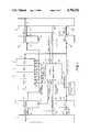
- FIG. 1sets forth a block diagram of the present invention dual port memory system in which a dual port memory gate array 10 includes a pair of read/write control inputs 40 and 41, a pair of data control outputs 45 and 43, a pair of address control outputs 44 and 42, a set of Row Address Strobe and Column Address Strobe outputs 35 (RAS/CAS), a set of write enable outputs 46, a pair of byte and bank select inputs 47 and 48 and an option control input 49.
- a memory array 16includes a quartet of individual memory banks 11, 12, 13 and 14 all of which are commonly coupled to a memory data bus terminal 15.
- Memory 16is constructed in accordance with conventional dynamic RAM memories, generally referred to as DRAM, in which a plurality of individual memory banks are combined and couple to a common memory data input/output terminal (in this case, terminal 15).
- Memory bank 11includes a RAS/CAS write enable input terminal 30 and a multiplexed address input 20.
- memory banks 12, 13 and 14include RAS/CAS write enable inputs 31, 32 and 33 respectively and multiplex address inputs 21, 22 and 23 respectively.
- a port A address buffer 50buffers and multiplexes the Row and Column address to the DRAM and includes a port A address bus input 51, a multiplex address output 52 and a address control signal input 53.
- Port A address bus input 51is coupled to the address bus output of processor A.
- Multiplex address bus output 52is coupled to inputs 20, 21, 22 and 23 of memory banks 11, 12, 13 and 14 respectively.
- Port B address buffer 70similar to address buffer 50 which also buffers and multiplexes the Row and Column address to the DRAM, includes an input address bus 71 and multiplexed output address bus 72 and an address control signal input 73.
- Bus 71is coupled to the address bus output of processor B and multiplexed address bus output 72 is coupled to inputs 20 through 23 of memory banks 11 through 14 respectively.
- Control signal input 73is coupled to output 42 of gate array 10.
- control input 53 of address buffer 50is coupled to output 44 of gate array 10.
- a data buffer 60constructed in accordance with conventional data buffer fabrication techniques, includes a data bus input 61, a memory data bus output 62 and a control signal input 63.
- a data buffer 80also of conventional data buffer fabrication, includes a data bus input 81, a memory data bus output 82 and a control signal input 83.
- gate array 10is formed of a plurality of logic gates arranged in a predetermined array and is fabricated in a manner whereby a plurality of individual gates are configured to produce a complex digital logic system which carries forward the functional activities set forth below in greater detail.
- the basic function of gate array 10 within the system shown in FIG. 1,is to control the transfer of information to and from memory 16. Accordingly, gate array 10 includes a pair of control signal lines coupled to address buffer 50 and data buffer 60 as well as a second pair of control signal lines coupled to address buffer 70 and data buffer 80.
- processor Awhich may comprise any number of individual central processing units but in its preferred form comprises either an Intel 80386 or 80286 processor, is coupled to address buffer 50 and data buffer 60 such and that all address and data information outputted by and received by processor A from memory array 16 is coupled through buffers 50 and 60.
- processor Aaccesses memory 16 by outputting a request which is applied to gate array 10 at terminal 40.
- an appropriate addressis placed on processor A address bus and is applied to address buffer 50 and data is either applied or received through data buffer 60 depending on the nature of the operations.
- processor Adesires to store information within memory 16 (write) or retrieve information from a specified location within memory 16 (read).
- processor Aretrieves information, that is to say executing a read from memory 16
- a read control signalis applied to terminal 40 of gate array 10 which creates a request by processor A to access memory 16.
- the address of the information sought to be read by processor Ais stored within address buffer 50 and data buffer 60 is configured to receive the incoming information anticipated once the read of memory 16 at the desired location is accomplished.
- no communication between processor A and memory 16takes place until gate array 10 provides the appropriate output signals, both to memory 16 and buffers 50 and 60 to facilitate the read.
- gate array 10determines that processor A may access memory 16
- the appropriate control signalsare produced at output temrinals 44 and 45 of gate array 10 and are applied to buffers 50 and 60.
- the application of control signals to buffer 50causes the address information in buffer 50 to be outputted to the multiplex address terminals 20 through 23 of memory 16.
- Certain bits of processor A's address bus 67are applied to input 47 of gate array 10 to determine which bank the requested operation will be performed in.
- gate array 10produces the appropriate RAS/CAS signal outputs to the appropriate memory bank to properly configure memory 16 to address the stored information sought by processor A in accordance with the memory address provided by buffer 50.
- the application of control signals to buffer 60causes the data from the memory data bus to be allowed to pass through the data buffer 60 to the Port A data bus terminal 65.
- each of banks 11, 12, 13 and 14 within memory 16are organized in a conventional multiplex configuration in which each address within the memory bank is uniquely defined by a row address and a column address.
- the particular bank from among banks 11 through 14is uniquely identified by the appropriate RAS/CAS signals.
- the output from address buffer 50comprises an appropriate row and column designation which combined with the RAS/CAS signals for that bank, uniquely identify the portion of memory 16 to e accessed.
- the RAS/CAS signalcauses the appropriate location within memory 16 to be read out on memory data bus terminal 15 which in turn is coupled by the memory data bus to input terminal 62 of data buffer 60.
- buffer 60needs no storage because processor A's internal clock is synchronous with that of the gate array.
- Buffer 80has storage for data going from memory to processor B because their clocks are not synchronous. Therefore, gate array 10 "leaves" the data in buffer 80 and disconnects from it. Processor B is then free to retrieve the data when it is ready.
- processor Breads information from memory 16 is substantially identical to that general process description set forth for processor A in that a request by processor B is applied to terminal 41 of gate array 10 and an appropriate address is applied to address buffer 70 while data is received through data buffer 80. Thereafter, in the event gate array 10 determines that the request of processor B may be granted, a pair of control signals are outputted at terminals 42 and 43 which couple the address information from address buffer 70 to memory 16 and which couple data buffer 80 to the memory bus terminal 15.
- a similar operationtakes place in the event of a processor request for a write operation, that is, a request by the processor to store data within a specified memory location.
- a write controlis coupled to terminal 40 of gate array 10 by processor A and an address is coupled to address buffer 50 while the desired data to be stored is applied to data buffer 60.
- gate array 10determines whether the request is to be granted and upon granting the access to processor A, the port A address bus is coupled from address buffer 50 to the multiplex address bus of memory 16 and certain address bits are applied to input 47 of gate array 10 while the appropriate RAS/CAS signal is outputted at terminal 35 of gate array 10 which configures the appropriate bank of memory 16 and defines the location within memory 16 into which information is to be written.
- data buffer 60coupled the port A data bus to output terminal 62 thereof and through the memory data bus to the memory data bus terminal 15 of memory 16.
- the write enable signals 46 of gate array 10are then activated and presented to the appropriate bank. Once the CAS signal has strobed the information into the appropriate address of memory 16, the write operation is complete and gate array 10 may accept another request for access to the memory.
- processor B in the write functionis essentially the same in that a write control signal is applied to input terminal 41 of gate array 10 while an address signal is coupled to address buffer 70 and the to-be-written data is applied to data buffer 80.
- the appropriate control signalsare applied to terminal 73 and 83 of buffers 70 and 80.
- the appropriate RAS/CAS signalis coupled to memory 16 and the information is transferred from data buffer 80 to input terminal 15 of memory 16 and strobed to the appropriate location by the CAS signal.
- the operationis complete and gate array 10 may once again accept a request from another processor.
- processor Athe system shown in FIG. 1 results in three systems attampting to access memory 16.
- These three systemsare processor A, processor B and the internal refresh system which, as mentioned above, is operative to periodically refresh the dynamic memory within memory 16.
- the refresh function of gate array 10is operative upon banks 11 through 14 of memory 16 independently.
- the individual refreshing of banks 11 through 14 of memory 16is carried forward in a staggered timing pattern such that at any given time during refresh, a single one of banks 11 through 14 is occupied by the refresh system leaving the remaining three banks operational.
- gate array 10may process a request by processor A or B to any of the three unoccupied banks within memory 16 notwithstanding the ongoing function of memory refresh taking place. As will be apparent, this provides considerable advantage over systems utilizing a refresh operation which is not staggered.
- the basic function of gate array 10is to resolve the conflict which results from simultaneously requests to access memory 16 from the three possible sources of processor A, processor B and the refresh system.
- gate array 10includes a logic system which does not require the multiple cycle times of the clock signals of processors A and B.
- gate array 10determines the priority of access in accordance with certain built-in decision rules that are embodied in the logic array. This set of logic rules are demonstrated below in the accompanying flow diagrams. However, suffice it to note here that gate array 10 functions essentially to grant the highest priority to a refresh request followed by resolution of conflicting requests between processors A and B in accordance with decisions which turn on whether the last access was given to the requesting processor as well as the question of whether the processor was denied request during the foregoing conflict of access.
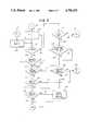
- FIG. 2sets forth the flow diagram for the internal logic of the present invention dual port memory controller during the initialization function.
- the dual port memory controllerutilizes a logic array rather than a serial program to make system decisions.
- the flow diagrams in FIGS. 2 through 6depict this decision process rather than a serial program.
- the initialization functionis initiated each time the system is "powered up", that is, at the start of each use of the system within which the dual port memory controller is operating.
- a reset function 85responds to the existence of a power up and initiates the reset function which is followed by an operaiton at block 86 in which the programmable option byte is serially loaded.
- this operationconfigures the dual port memory controller gate array (seen in FIG. 1) for the different operations relating to the particular processors used for processors A and B (seen in FIG. 1).
- function 86describes the operative environment to the dual port memory controller.
- the operationmoves to a decision function 87 in which a determination is made as to whether a external refresh request is present.
- the refresh systemruns independently in response to its own timing clocks in order to assure that the memory is periodically refreshed in accordance with the requirements of a dynamic RAM.
- branch 95 and function 94in which an externally generated refresh mode is initiated. This function operates to inform the refresh timer circuit that acceptance should be given to external refresh signals.
- function block 94the system returns to function block 89.
- the systemcontinues through branch 96 to function 88 in which an internally generated refresh mode is undertaken. This operation tells the refresh timer circuit to generate internal refresh signals rather than look for external refresh signals. Thereafter, the system moves to function 89.
- function 89the memory initialization, refresh warm-up cycles are initiated. In essence, this function provides a predetermined number of refresh cycles to the dynamic RAM which are required to assure that the dynamic RAM is initialized.
- a decision block 90the system moves to a decision block 90 in which a determination is made as to whether the predetermined number of warm-up cycles have been completed.
- the systementers the port A access system 91.
- gate array 10automatically selects port A in the absence of any conflicting instruction.
- the systemmoves to port A idle function 100 and decision block 101 in which a determination is made as to whether any requests are present in the system.
- the systembranches at branch 107 and reports to port A idle function 100. This looping operation continues until a request is present, at which time the system continues at branch 108 to decision function 102 in which a determination is made as to whether the request is a refresh request.
- the systembranches at branch 109 to a decision function 117 in which a determination is made as to whether there are any other requests present in the system. In the event no other requests are simultaneously requested, the system branches at branch 119 to refresh input 92 (seen in FIG. 6). In the event other requests are present in the system, the system branches at branch 120 to decision function 118 in which a determination is made as to whether the other request within the system is directed to the same bank as refresh is requested for. In the event that the request is directed to the same bank as refresh, the system branches at branch 121 and returns to refresh initiation 92. In the event the request is for a different bank than refresh, the system branches at branch 122 and the refresh operation 92 is simultaneously performed while the main system flow returns to branch 110.
- decision function 102determines whether the request within the system determined in function 101 is not a refresh request.
- the systemcontinues at branch 110 to a decision function 103 in which a determination is made as to whether any requests have been queued.
- the systembranches at branch 111 to a decision function at branch 123 in which the determination is made as to whether the queued request is a port A request.
- the systemreturns via branch 126 to branch 114.
- the systembranches via branch 125 to the select B function 124 (seen in FIG. 4).
- a decision function 104in which a determination is made as to whether a port A request is present. In the event no port A request is determined, the system branches at branch 113 and returns to B select function 124. If the request is a port A request, the system continues via branch 114 to a decision function 105. In decision function 105, a determination is made as to whether a port B request is present. In the event a port B request has been made, the system branches at branch 115 to a function block 127 in which the port B request is queued. In the event a port B request is not present, the system continues to the memory cycle function input at 106 (seen in FIG. 5).
- the systemmoves to port B idle function 200 and decision block 201 in which a determination is made as to whether any requests are present in the system.
- the systembranches at branch 207 and reports to port B idle function 200. This looping operation continues until a request is present, at which time the system continues at branch 208 to decision function 202 in which a determination is made as to whether the request is a refresh request.
- the systembranches at branch 209 to a decision function 217 in which a determination is made as to whether there are any other requests present in the system.
- the systembranches at branch 219 to refresh input 92 (seen in FIG. 6).
- the systembranches at branch 220 to decision function 218 in which a determination is made as to whether the other request within the system is directed to the same bank as refresh is requested for.
- the systembranches at branch 221 and returns to refresh initiation 92.
- the system branches at branch 222 and the refresh operaiton 92is simultaneously performed while the main system flow returns to branch 210.
- decision function 202determines whether the other request within the system determined in function 201 is not a refresh request.
- the systemcontinues at branch 210 to a decision function 203 in which a determination is made as to whether any requests have been queued.
- the systembranches at branch 211 to a decision function at branch 223 in which the determination is made as to whether the queued request is a port B request.
- the systemreturns via branch 226 to branch 214.
- the systembranches via branch 225 to the select A function 128 (seen in FIG. 3).
- the systemcontinues via branch 212 to a decision function 204 in which a determination is made as to whether a port B request is present. In the event no port B request is determined, the system branches at branch 213 and returns to B select function 128. If the request is a port B request, the system continues via branch 214 to a decision function 205. In decision function 205, a determination is made as to whether a port A request is present. In the event a port A request has been made, the system branches at branch 215 to a function block 227 in which the port A request is queued. In the event a port A request is not present, the system continues to the memory cycle function input at 106 (seen in FIG. 5).
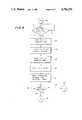
- FIG. 5sets forth the flow diagram for a memory cycle of the present invention dual port memory controller initiated at a memory input 106. Thereafter, the system moves to a decision function 130 in which a determination is made as to whether the appropriate precharge interval has passed.
- the precharge intervalis a requirement of the DRAM in memory 16 and is described in more detail in the discussion of FIG. 7.
- the systemreturns by branch 131 to decision function 130.
- the precharge intervalhas passed the system branches by branch 132 to a function 133 in which the RAS signal is issued to the selected bank.
- the systemcarries forward to function 134 in which the appropriate address control signals are changed from row address to column address control.
- a function 135is carried forward in which the CAS signal is issued to the selected bank.
- a function 136is carried forward in which the cycle grant signal is issued which signals the completion of the cycle and enables the arbitrator to prepare for another request.
- the systemnext moves to a function 137 in which the precharge counter for the selected bank is reset which initiates the countdown to determine when a new RAS signal may be issued to that particular bank.
- the systemnext moves to a decision function 138 in which a determination is made as to whether port A is selected. In the event port A is selected, the system moves by a branch 140 to port A initiation 91. In the event port A is not selected, the system moves to port B initiation 191 by a branch 139.
- FIG. 6sets forth the flow diagram of a refresh cycle of the present invention dual port memory controller in which a refresh initiation 92 begins the refresh cycle.
- the systemnext moves to a decision function 145 in which a determination is made as to whether the selected bank of the memory has completed its precharge interval. In the event the precharge interval has not passed, the system branches at branch 146 and returns to decision function 145. In the event the precharge interval has passed, the system continues at branch 147 to function 148 in which the CAS signal is issued to the selected bank.
- the present invention systemgenerates a CAS before RAS during refresh cycles because the gate array does not generate memory address during any cycle, whether refresh or processor cycle. Normal RAS only refreshes require that the row address be presented to the DRAM.
- the systemmoves to function 149 in which the RAS signal is applied to the selected memory bank.
- the systemmoves to a function 150 in which the refresh grant is issued to the arbitrator.
- the systemmoves to a function 151 in which the refresh timer is reset.
- the systemmoves to a function 152 in which the precharge count for the selected bank counter is reset to implement the precharge interval determination.
- the systemmoves to a decision function 153 in which a determination is made as to whether the preceding refresh cycle was an initialization cycle. In the event the previous refresh cycle was part of the initialization cycle set forth in FIG. 2, the system branches at branch 154 to initiation branch 93.
- the systemcontinues at branch 155 to a decision function 156 in which a determination is made as to whether port A has been selected.
- the systembranches at branch 157 to port B arbitration 191 (seen in FIG. 4).
- the systemmoves to branch 158 and to port A arbitration input 91.
- FIG. 7sets forth a block diagram representation of gate array 10 shown in FIG. 1.
- a port A command decode 160includes an input 231 coupled to input 40 of gate array 10 and an output 232.
- a port B command decode 161includes an input 233 coupled to input 41 of gate array 10 and an output 234.
- a bank select circuit 162includes an input 235 coupled to inputs 47 and 48 of gate array 10. and an output 236.
- a byte control 163includes an input 237 coupled to inputs 47 and 48 of gate array 10 and an output 238.
- a system options circuit 164includes an input 239 coupled to input 49 of gate array 10 and an output 240.
- An arbitration/port selection control 175includes an input 243 coupled to output 232, an input 242 coupled to output 234, an input 241 coupled to output 236, and an input 249 coupled to output 240.
- Arbitration/port selection control 175further includes inputs 244, 245 and 248 together with outputs 246 and 247.
- a refresh timer 173includes an input 278 coupled to output 240 and an output 279 coupled to input 248.
- a request queue 170includes an input 250 coupled to output 232, an input 251 coupled to output 234 and an output 252 coupled to input 244.
- a precharge counter 171includes an input 254 and an output 253 coupled to input 245 of arbitration/port selection control 175.
- a quartet of memory cycle sequencers 180, 181, 182 and 183define respective inputs 255, 256, 257 and 258 commonly coupled to output 246.
- Memory cycle sequencers 180 through 183further define respective outputs 261 through 264 respectively which are commonly coupled to input 254 of precharge counter 171.
- a refresh cycle sequencer 174includes an input 260 coupled to output 247, an input 259 coupled to output 279, an an output 265 coupled to input 254 of precharge counter 171.
- An address control 184includes an input 266 coupled to outputs 261 through 265 and an output 273 coupled to outputs 42 and 44 of gate array 10.
- An acknowledge control 185includes an input 267 coupled to outputs 261 through 265 and an output 274 coupled to outputs 40 and 41 of gate array 10.
- a RAS/CAS control 186includes an input 268 coupled to outputs 261 through 265 and an output 275 coupled to outut 35 of gate array 10.
- a data control 187includes an input 269 coupled to outputs 261 through 265, an input 270 coupled to output 238 of byte control 163, and an output 276 coupled to outputs 43 and 45 of gate array 10.
- a write control 188includes an input 271 coupled to output 261 through 265, an input 272 coupled to output 238 of byte control 163, and an output 277 coupled to output 46 of gate array 10.
- port A command decode 160receives the read/write signals from processor 17 (port A) and determines from the applied signal whether a memory request in being made by the processor. In the event the port A request circuit determines that a memory request is being made by processor 17, it produces a signal indicative of the request which is applied to input 243 of arbitration/port selection control 175. In accordance with the invention, the port A request is commonly coupled to input 250 of request queue circuit 170. Similarly, port B command decode 161 is coupled to processor 18 (port B) and receives similar read/write signals from port B processor 18. In similar fashion to port A command decode 160, port B command decode 161 determines whether a memory request is being made by processor 18. In the event a request is being made, port B command decode 161 applies an indicative signal to input 242 of arbitration/port selection control 175 and to input 251 of request queue 170.
- Bank select 162receives the address signals from processor A (17) and processor B (18) through inputs 47 and 48 of gate array 10 and examines the lower address lines of ports A and B to determine which bank of memory a memory request is directed to.
- the address signal applied to address bus inputs 47 and 48 of gate array 10comprises a plurality of binary words organized to provide information indicative of the selected one of banks 11, 12, 13 and 14 (seen in FIG. 1) within memory 16 together with the specific address within the selected bank to uniquely indentify the portion of memory 16 to which memory access is requested.
- bank select 162initially examines the request at the appropriate portion thereof which permits a determination as to which memory bank is the subject of the request for access. In response to the determination of the appropriate bank, bank select 162 produces a bank select signal which is coupled to input 241 of arbitration/port selection control 175 to identify the selected bank.
- Byte control 163is coupled to processors 17 and 18 and is operative to determine which bytes within the memory address for which access is requested will be active during the transfer of information to or from the memory. In accordance with conventional computing techniques, only those portions of the stored information within the memory address which are to be changed will be active during the transfer of information to or from memory 16. Byte control 163 upon determination of the bytes which will be active during the transfer produces an output comprising an internal byte enable signal which is coupled to data control 187 and write control 188.
- system options circuit 164is coupled to the initialization portion of the host computer (not shown) which provides initialization information as to the processor types utilized for processors 17 and 18 as well as other operating parameter such as the number of wait states and the refresh interval operative upon memory 16.
- the primary function of system options circuit 164is to provide a conversion of the serially configured system options information applied to input terminal 239 to a parallel configured information signal at output 240.
- the use of serial to parallel conversion within system options 164is primarily utilized to reduce the number of external connections required to the operating environment of gate array 10 (seen in FIG. 1).
- Request queue circuit 170receives the memory access requests generated by port A and port B command decode circuits 160 and 161 respectively and places them in a queue in the event that the memory access requests cannot be immediately serviced.
- the present invention dual port memory controllerresolves and prioritizes simultaneous requests for access to memory 16. Such simultaneous requests may, for example, result in the event one processor is currently doing a memory cycle at the time the other processor request is presented or in the event a refresh cycle is operative upon memory 16 at the time the memory request is presented.
- the requestsare initially queued within request queue 170 during the time arbitration and port selection control 175 is determining whether the request may be granted. In the event a request is granted the queued request is deleted from request queue 170. In the event the request cannot be granted, the queued request remains within request queue 170.
- Precharge counter 171includes a conventional bank of counters for each of banks 11 through 14 within memory 16 (seen in FIG. 1).
- the counters(not shown) are reset upon the completion of each memory cycle with the associated bank and are incremented by successive system clock pulses in accordance with the precharge setting provided by system options 164 during initialization as described above.
- the function of precharge counter circuit 171is to inhibit the initiation of a new memory cycle in the same bank as the memory cycle until a predetermined time period has elapsed. This time period which is selected in accordance with the characteristics of the memory mechanism utilized in memory 16 is referred as the RAS precharge time.
- Refresh timer 173includes a timing circuit which periodically generates refresh requests to refresh the dynamic memory within memory 16.
- the use of refresh timer 173 and its constructioncomprises an important aspect of the present invention in that individual refresh of banks 11 through 14 within memory 16 is undertaken in a staggered sequential timing thereby eliminating the simultaneous operation of refresh cycles upon all of the banks within memory 16. This staggered operation assures that the RAS and CAS operations will not occur simultaneously. This latter effect is particularly beneficial in eliminating the production of undesired noise within the system.
- Arbitration/port selection control 175comprises a dedicated system gate array which in accordance with the invention is optionable but not programmable that is to say, the system is not controlled by a processor. Accordingly, the basic decision functions as set forth in the flow diagrams of FIGS. 2 through 6 inclusive, is carried forward to determine the priorization of conflicting requests for access to memory 16.
- a substantial advantage of the present invention system in resolving or arbitrating between conflicting requests for memory accessis realized by the use of a dedicated system system with the particular processor being used.
- system systems of the type used in conventional memory controllersare configured to accept many types of processors. The capability of accepting different processors results in lengthier decision processes.
- arbitration/port selection control 175arbitrates between port A and port B requests, queued port A and port B requests and refresh requests to grant access to memory 16 in accordance with the process set forth in the flow diagrams of FIGS. 2 through 6, inclusive.
- arbitration/port selection control 175can permit a memory cycle or access to occur in one bank while a refresh cycle is occurring in another bank. This is extremely advantageous in that system noise is reduced due to the switching of smaller RAS and CAS currents.
- Memory cycle sequencers 180, 181, 182 and 183are of identical construction and function and are individually operable upon memory banks 11, 12, 13 and 14 respectively of memory 16.
- the memory cycle sequencerscontrol the timing of events within a memory cycle.
- the memory cycle sequencerIn response to control signals from arbitration/port selection control 175 and the read or write select signal, the memory cycle sequencer produces a series of properly timed signals to perform a memory cycle.
- memory cycle sequencers 180 through 183are constructed and operative in accordance with conventional memory cycle sequencer fabrication and produce the required control of the memory address strobing, the RAS and CAS signals, and the read/write signals operable to transfer information to or from the individual banks of memory 16.
- Refresh cycle sequencer 174is operative in response to the timing signal from refresh timer 173 which triggers the request to arbitration/port selection control 175 for the initiation of a refresh cycle.
- arbitration/port selection control 175thereafter produces an enable signal which is applied to refresh cycle sequencer 174 causing it to initiate a refresh cycle on the memory banks of memory 16 in accordance with the above-described staggered refresh system.
- Refresh cycle sequencer 174comprises a timing signal generating circuit which produces the required CAS and RAS signals in much the same manner as the foregoing described memory cycle sequencers 180 through 183. as mentioned above in connection with FIG. 6, refresh cycle sequencer 174 performs CAS operation prior to RAS operation.
- Address control 184is operative in response to the output signals of memory cycle sequencers 180 through 183 to control the external address buffers and multiplexers of the present invention system and select the appropriate address for application to the memory array. Address control 184 produces the required output signals necessary to gate the proper row or column addresses to the selected bank of memory 16 to which access is granted.
- Acknowledge control 185responds to memory cycle sequencers 180 through 183 to determine the completion of a memory cycle and produce an output signal which is coupled to terminals 40 and 41 of gate array 10 which in turn are coupled to processor A (17) or processor B (18) to indicate the completion of the memory cycle.
- RAS/CAS control 186responds to memory cycle sequencers 180 through 183 or refresh cycle sequencer 174 to produce the appropriate RAS and CAS signals in proper synchronization to the system clock signals for effective strobing of the memory during the memory or refresh cycles.
- the output from RAS/CAS control 186comprises the strobe signals which strobes in the row address or column address of the address within memory 16 to which or from which information is to be transferred.
- Data control 187responds to byte control 163 and memory cycle sequencers 180 through 183 to control the number of bytes within the selected address of memory 16 which are to be activated.
- byte control 163provides information to data control 187 indicating the byte to be activated while memory cycle sequencers 180 through 183 indicate the timing applicable to the transfer of the information byte to the memory address.
- Data control 187produces four data enable signals which are applied to data buffers 60 and 80 (seen in FIG. 1).
- Write control 188responds to byte control 163 to select the byte within the selected memory address to which information will be written. The timing of information transfer is controlled by the signals provided by memory cycle sequencers 180 through 183. Write control 188 produces a write signal in the event information is to be transferred to memory 16. In the absence of a write signal from write control 188, the system will initiate a read of the selected address within memory 16.
Landscapes
- Engineering & Computer Science (AREA)
- Microelectronics & Electronic Packaging (AREA)
- Theoretical Computer Science (AREA)
- Physics & Mathematics (AREA)
- General Engineering & Computer Science (AREA)
- General Physics & Mathematics (AREA)
- Computer Hardware Design (AREA)
- Dram (AREA)
Abstract
Description
Claims (8)
Priority Applications (1)
| Application Number | Priority Date | Filing Date | Title |
|---|---|---|---|
| US07/111,428US4796232A (en) | 1987-10-20 | 1987-10-20 | Dual port memory controller |
Applications Claiming Priority (1)
| Application Number | Priority Date | Filing Date | Title |
|---|---|---|---|
| US07/111,428US4796232A (en) | 1987-10-20 | 1987-10-20 | Dual port memory controller |
Publications (1)
| Publication Number | Publication Date |
|---|---|
| US4796232Atrue US4796232A (en) | 1989-01-03 |
Family
ID=22338493
Family Applications (1)
| Application Number | Title | Priority Date | Filing Date |
|---|---|---|---|
| US07/111,428Expired - Fee RelatedUS4796232A (en) | 1987-10-20 | 1987-10-20 | Dual port memory controller |
Country Status (1)
| Country | Link |
|---|---|
| US (1) | US4796232A (en) |
Cited By (143)
| Publication number | Priority date | Publication date | Assignee | Title |
|---|---|---|---|---|
| US4887240A (en)* | 1987-12-15 | 1989-12-12 | National Semiconductor Corporation | Staggered refresh for dram array |
| US4888741A (en)* | 1988-12-27 | 1989-12-19 | Harris Corporation | Memory with cache register interface structure |
| WO1990002991A1 (en)* | 1988-09-13 | 1990-03-22 | Silicon Graphics, Inc. | Graphics processor with staggered memory timing |
| WO1990005364A1 (en)* | 1988-11-10 | 1990-05-17 | Dallas Semiconductor Corporation | Self-timed sequential-access multiport memory |
| US4951246A (en)* | 1989-08-08 | 1990-08-21 | Cray Research, Inc. | Nibble-mode dram solid state storage device |
| US4967397A (en)* | 1989-05-15 | 1990-10-30 | Unisys Corporation | Dynamic RAM controller |
| US4975880A (en)* | 1988-05-02 | 1990-12-04 | Tektronix, Inc. | Memory system for storing data from variable numbers of input data streams |
| US4977494A (en)* | 1989-02-17 | 1990-12-11 | Hughes Aircraft Company | High speed digital motion controller architecture |
| US4999768A (en)* | 1987-04-14 | 1991-03-12 | Mitsubishi Denki Kabushiki Kaisha | Data transfer control units each of which comprises processors and dual-part memory |
| EP0409330A3 (en)* | 1989-07-19 | 1991-04-24 | Philips Patentverwaltung Gmbh | Memory access control circuit |
| US5012445A (en)* | 1987-10-13 | 1991-04-30 | Hitachi, Ltd. | Programmable read only memory being capable of controlling internal writing voltage of external voltage |
| US5057998A (en)* | 1987-04-14 | 1991-10-15 | Mitsubishi Denki Kabushiki Kaisha | Data transfer control unit |
| US5072420A (en)* | 1989-03-16 | 1991-12-10 | Western Digital Corporation | FIFO control architecture and method for buffer memory access arbitration |
| US5089987A (en)* | 1989-03-30 | 1992-02-18 | Mitsubishi Denki Kabushiki Kaisha | Refresh control circuit |
| US5097445A (en)* | 1989-03-03 | 1992-03-17 | Mitsubishi Denki Kabushiki Kaisha | Semiconductor integrated circuit with selective read and write inhibiting |
| EP0473388A3 (en)* | 1990-08-29 | 1992-05-06 | Mitsubishi Denki Kabushiki Kaisha | A dynamic type semiconductor memory device with a refresh function and method for refreshing the same |
| US5115411A (en)* | 1990-06-06 | 1992-05-19 | Ncr Corporation | Dual port memory system |
| US5197142A (en)* | 1988-06-17 | 1993-03-23 | Dallas Semiconductor Corp. | Memory arbitration between timekeeping circuitry and general purpose computer |
| US5216635A (en)* | 1991-07-24 | 1993-06-01 | Ncr Corporation | System and method for requesting access to a computer memory for refreshing |
| US5226166A (en)* | 1989-02-10 | 1993-07-06 | Mitsubishi Denki K.K. | Parallel operation processor with second command unit |
| US5235691A (en)* | 1989-09-01 | 1993-08-10 | Oki Electric Industry Co., Ltd. | Main memory initializing system |
| US5251177A (en)* | 1989-01-23 | 1993-10-05 | Matsushita Electric Industrial Co., Ltd. | Semiconductor memory device having an improved refresh operation |
| US5253214A (en)* | 1991-09-27 | 1993-10-12 | Eastman Kodak Company | High-performance memory controller with application-programmable optimization |
| US5265231A (en)* | 1991-02-08 | 1993-11-23 | Thinking Machines Corporation | Refresh control arrangement and a method for refreshing a plurality of random access memory banks in a memory system |
| US5276858A (en)* | 1991-12-26 | 1994-01-04 | Intel Corporation | Memory controller with integrated delay line circuitry |
| US5303360A (en)* | 1991-02-22 | 1994-04-12 | Vlsi Technology, Inc. | Programmable boundary between system board memory and slot bus memory |
| EP0591695A1 (en)* | 1992-09-18 | 1994-04-13 | Hitachi, Ltd. | Processor system using synchronous dynamic memory |
| US5317501A (en)* | 1987-10-13 | 1994-05-31 | Bernhard Hilpert | Control system for a numerically controlled machine |
| US5335336A (en)* | 1988-03-28 | 1994-08-02 | Hitachi, Ltd. | Memory device having refresh mode returning previous page address for resumed page mode |
| US5345577A (en)* | 1989-10-13 | 1994-09-06 | Chips & Technologies, Inc. | Dram refresh controller with improved bus arbitration scheme |
| US5345574A (en)* | 1990-05-15 | 1994-09-06 | Seiko Epson Corporation | Memory card having controller providing adjustable refresh to a plurality of DRAMs |
| US5392441A (en)* | 1989-01-27 | 1995-02-21 | Compaq Computer Corporation | Pump bus to avoid indeterminacy in reading variable bit field |
| US5398211A (en)* | 1993-10-14 | 1995-03-14 | Integrated Device Technology, Inc. | Structure and method for providing prioritized arbitration in a dual port memory |
| US5404464A (en)* | 1993-02-11 | 1995-04-04 | Ast Research, Inc. | Bus control system and method that selectively generate an early address strobe |
| US5414666A (en)* | 1991-07-31 | 1995-05-09 | Ezel Inc. | Memory control device |
| US5428745A (en)* | 1992-06-12 | 1995-06-27 | Dow Benelux N.V. | Secure communication system for re-establishing time limited communication between first and second computers before communication time period expiration using new random number |
| US5440711A (en)* | 1990-03-05 | 1995-08-08 | Mitsubishi Denki Kabushiki Kaisha | Method for controlling DRAM memory in a microcomputer |
| US5455920A (en)* | 1989-12-04 | 1995-10-03 | Mitsubishi Denki Kabushiki Kaisha | Multiprocessor system having offset address setting |
| US5463755A (en)* | 1991-05-15 | 1995-10-31 | International Business Machines Corporation | High-performance, multi-bank global memory card for multiprocessor systems |
| US5465339A (en)* | 1991-02-27 | 1995-11-07 | Vlsi Technology, Inc. | Decoupled refresh on local and system busses in a PC/at or similar microprocessor environment |
| US5519603A (en)* | 1992-06-12 | 1996-05-21 | The Dow Chemical Company | Intelligent process control communication system and method having capability to time align corresponding data sets |
| US5528463A (en)* | 1993-07-16 | 1996-06-18 | Dallas Semiconductor Corp. | Low profile sockets and modules for surface mountable applications |
| US5544078A (en)* | 1988-06-17 | 1996-08-06 | Dallas Semiconductor Corporation | Timekeeping comparison circuitry and dual storage memory cells to detect alarms |
| US5568615A (en)* | 1992-06-12 | 1996-10-22 | The Dow Chemical Company | Stealth interface for process control computers |
| US5579206A (en)* | 1993-07-16 | 1996-11-26 | Dallas Semiconductor Corporation | Enhanced low profile sockets and module systems |
| US5586289A (en)* | 1994-04-15 | 1996-12-17 | David Sarnoff Research Center, Inc. | Method and apparatus for accessing local storage within a parallel processing computer |
| US5603061A (en)* | 1991-07-23 | 1997-02-11 | Ncr Corporation | Method for prioritizing memory access requests using a selected priority code |
| US5629907A (en)* | 1991-06-18 | 1997-05-13 | Dallas Semiconductor Corporation | Low power timekeeping system |
| US5636358A (en)* | 1991-09-27 | 1997-06-03 | Emc Corporation | Method and apparatus for transferring data in a storage device including a dual-port buffer |
| US5659711A (en)* | 1991-03-13 | 1997-08-19 | Mitsubishi Denki Kabushiki Kaisha | Multiport memory and method of arbitrating an access conflict therein |
| US5669009A (en)* | 1994-06-30 | 1997-09-16 | Hughes Electronics | Signal processing array |
| US5721722A (en)* | 1995-05-31 | 1998-02-24 | Mitsubishi Denki Kabushiki Kaisha | FA controller and data processing method therefor |
| US5724540A (en)* | 1988-03-28 | 1998-03-03 | Hitachi, Ltd. | Memory system having a column address counter and a page address counter |
| US5801998A (en)* | 1995-11-06 | 1998-09-01 | Hyundai Electronics Industries Co., Ltd. | Dynamic random access memory |
| US5887270A (en)* | 1995-11-21 | 1999-03-23 | Emc Corporation | Fault tolerant controller system and method |
| US5897656A (en)* | 1996-09-16 | 1999-04-27 | Corollary, Inc. | System and method for maintaining memory coherency in a computer system having multiple system buses |
| US5953743A (en)* | 1997-03-12 | 1999-09-14 | Micron Electronics, Inc. | Method for accelerating memory bandwidth |
| US6032232A (en)* | 1997-05-29 | 2000-02-29 | 3Com Corporation | Multiported memory access system with arbitration and a source burst limiter for blocking a memory access request |
| US6049847A (en)* | 1996-09-16 | 2000-04-11 | Corollary, Inc. | System and method for maintaining memory coherency in a computer system having multiple system buses |
| US6052327A (en)* | 1997-10-14 | 2000-04-18 | Altera Corporation | Dual-port programmable logic device variable depth and width memory array |
| WO2000043895A1 (en)* | 1999-01-22 | 2000-07-27 | Analog Devices, Inc. | Dram refresh monitoring and cycle accurate distributed bus arbitration in a multi-processing environment |
| US6173353B1 (en)* | 1996-07-01 | 2001-01-09 | Sun Microsystems, Inc. | Method and apparatus for dual bus memory transactions |
| US6202137B1 (en)* | 1997-09-18 | 2001-03-13 | Intel Corporation | Method and apparatus of arbitrating requests to a multi-banked memory using bank selects |
| US6212607B1 (en)* | 1997-01-17 | 2001-04-03 | Integrated Device Technology, Inc. | Multi-ported memory architecture using single-ported RAM |
| EP0770961A3 (en)* | 1995-10-24 | 2001-04-11 | Konica Corporation | Memory access system |
| US6219769B1 (en) | 1998-12-09 | 2001-04-17 | Advanced Micro Devices, Inc. | Method and system for origin-sensitive memory control and access in data processing systems |
| US6226721B1 (en) | 1998-12-09 | 2001-05-01 | Advanced Micro Devices, Inc. | Method and system for generating and utilizing speculative memory access requests in data processing systems |
| US6260123B1 (en) | 1998-12-09 | 2001-07-10 | Advanced Micro Devices, Inc. | Method and system for memory control and access in data processing systems |
| US6298413B1 (en) | 1998-11-19 | 2001-10-02 | Micron Technology, Inc. | Apparatus for controlling refresh of a multibank memory device |
| US6381683B1 (en)* | 1998-12-09 | 2002-04-30 | Advanced Micro Devices, Inc. | Method and system for destination-sensitive memory control and access in data processing systems |
| EP1220226A3 (en)* | 2000-12-20 | 2002-12-18 | Fujitsu Limited | Multi-port memory based on DRAM core |
| US6510497B1 (en) | 1998-12-09 | 2003-01-21 | Advanced Micro Devices, Inc. | Method and system for page-state sensitive memory control and access in data processing systems |
| US6545935B1 (en)* | 2000-08-29 | 2003-04-08 | Ibm Corporation | Dual-port DRAM architecture system |
| US6546439B1 (en) | 1998-12-09 | 2003-04-08 | Advanced Micro Devices, Inc. | Method and system for improved data access |
| US6587918B1 (en)* | 1998-11-19 | 2003-07-01 | Micron Technology, Inc. | Method for controlling refresh of a multibank memory device |
| US20030135699A1 (en)* | 2000-12-20 | 2003-07-17 | Yasurou Matsuzaki | Multi-port memory based on DRAM core |
| US6914841B1 (en)* | 2004-01-30 | 2005-07-05 | Infineon Technologies Ag | System and method for refreshing a dynamic memory device |
| US20050154820A1 (en)* | 2004-01-12 | 2005-07-14 | Briggs Theodore C. | Memory controller connection to RAM using buffer interface |
| US6920535B1 (en)* | 2000-05-16 | 2005-07-19 | Intel Corporation | Accessing multi-ported memory for uncached status and control accesses |
| US20060041704A1 (en)* | 2004-08-23 | 2006-02-23 | Choi Joo S | Dual port memory with asymmetric inputs and outputs, device, system and method |
| US7111110B1 (en) | 2002-12-10 | 2006-09-19 | Altera Corporation | Versatile RAM for programmable logic device |
| US20070011387A1 (en)* | 2005-07-11 | 2007-01-11 | Via Technologies Inc. | Flexible width data protocol |
| US20070011378A1 (en)* | 2005-07-11 | 2007-01-11 | Via Technologies, Inc. | Apparatus and method for quad-pumped address bus |
| US20070011377A1 (en)* | 2005-07-05 | 2007-01-11 | Via Technologies, Inc. | Microprocessor apparatus and method for enabling variable width data transfers |
| US20070022239A1 (en)* | 2005-07-19 | 2007-01-25 | Via Technologies Inc. | Apparatus and method for ordering transaction beats in a data transfer |
| US7171525B1 (en)* | 2002-07-31 | 2007-01-30 | Silicon Image, Inc. | Method and system for arbitrating priority bids sent over serial links to a multi-port storage device |
| US20070028021A1 (en)* | 2005-07-19 | 2007-02-01 | Via Technologies, Inc. | Apparatus and method for sparse line write transactions |
| US20070058471A1 (en)* | 2005-09-02 | 2007-03-15 | Rajan Suresh N | Methods and apparatus of stacking DRAMs |
| US20070143031A1 (en)* | 2003-08-30 | 2007-06-21 | Istech Co., Ltd. | Method of analyzing a bio chip |
| US20070147162A1 (en)* | 2005-12-22 | 2007-06-28 | Samsung Electronics Co., Ltd. | Multi-port semiconductor memory device having variable access paths and method therefor |
| US20070171755A1 (en)* | 2005-12-22 | 2007-07-26 | Samsung Electronics Co., Ltd. | Semiconductor memory device and method therefor |
| US20070195633A1 (en)* | 2006-02-21 | 2007-08-23 | Samsung Electronics Co., Ltd. | Multi-port semiconductor memory device and signal input/output method therefor |
| US20070195613A1 (en)* | 2006-02-09 | 2007-08-23 | Rajan Suresh N | Memory module with memory stack and interface with enhanced capabilities |
| US20070204075A1 (en)* | 2006-02-09 | 2007-08-30 | Rajan Suresh N | System and method for reducing command scheduling constraints of memory circuits |
| US20080010435A1 (en)* | 2005-06-24 | 2008-01-10 | Michael John Sebastian Smith | Memory systems and memory modules |
| US20080028136A1 (en)* | 2006-07-31 | 2008-01-31 | Schakel Keith R | Method and apparatus for refresh management of memory modules |
| US20080025108A1 (en)* | 2006-07-31 | 2008-01-31 | Metaram, Inc. | System and method for delaying a signal communicated from a system to at least one of a plurality of memory circuits |
| US20080028137A1 (en)* | 2006-07-31 | 2008-01-31 | Schakel Keith R | Method and Apparatus For Refresh Management of Memory Modules |
| US20080027702A1 (en)* | 2005-06-24 | 2008-01-31 | Metaram, Inc. | System and method for simulating a different number of memory circuits |
| US20080056014A1 (en)* | 2006-07-31 | 2008-03-06 | Suresh Natarajan Rajan | Memory device with emulated characteristics |
| US20080062773A1 (en)* | 2006-07-31 | 2008-03-13 | Suresh Natarajan Rajan | System and method for simulating an aspect of a memory circuit |
| US20080086588A1 (en)* | 2006-10-05 | 2008-04-10 | Metaram, Inc. | System and Method for Increasing Capacity, Performance, and Flexibility of Flash Storage |
| US20080115006A1 (en)* | 2006-07-31 | 2008-05-15 | Michael John Sebastian Smith | System and method for adjusting the timing of signals associated with a memory system |
| USRE40423E1 (en) | 1996-07-29 | 2008-07-08 | Xilinx, Inc. | Multiport RAM with programmable data port configuration |
| US20080183974A1 (en)* | 2007-01-31 | 2008-07-31 | Dell Products, Lp | Dual Ported Memory with Selective Read & Write Protection |
| US20080239857A1 (en)* | 2006-07-31 | 2008-10-02 | Suresh Natarajan Rajan | Interface circuit system and method for performing power management operations in conjunction with only a portion of a memory circuit |
| US20090049250A1 (en)* | 2007-08-15 | 2009-02-19 | Micron Technology, Inc. | Memory device and method having on-board processing logic for facilitating interface with multiple processors, and computer system using same |
| US20090049245A1 (en)* | 2007-08-15 | 2009-02-19 | Micron Technology, Inc. | Memory device and method with on-board cache system for facilitating interface with multiple processors, and computer system using same |
| US20090049264A1 (en)* | 2007-08-15 | 2009-02-19 | Micron Technology, Inc. | Memory device and method having on-board address protection system for facilitating interface with multiple processors, and computer system using same |
| US20090106503A1 (en)* | 2007-10-23 | 2009-04-23 | Dong-Hyuk Lee | Method, device, and system for preventing refresh starvation in shared memory bank |
| CN100530418C (en)* | 2000-12-20 | 2009-08-19 | 富士通微电子株式会社 | Multi-port memory based on DRAM core |
| US20090285031A1 (en)* | 2005-06-24 | 2009-11-19 | Suresh Natarajan Rajan | System and method for simulating an aspect of a memory circuit |
| US7730338B2 (en) | 2006-07-31 | 2010-06-01 | Google Inc. | Interface circuit system and method for autonomously performing power management operations in conjunction with a plurality of memory circuits |
| US20110055451A1 (en)* | 2006-07-27 | 2011-03-03 | Ware Frederick A | Cross-threaded memory system |
| US20110095783A1 (en)* | 2009-06-09 | 2011-04-28 | Google Inc. | Programming of dimm termination resistance values |
| US8077535B2 (en) | 2006-07-31 | 2011-12-13 | Google Inc. | Memory refresh apparatus and method |
| US8080874B1 (en) | 2007-09-14 | 2011-12-20 | Google Inc. | Providing additional space between an integrated circuit and a circuit board for positioning a component therebetween |
| US8081474B1 (en) | 2007-12-18 | 2011-12-20 | Google Inc. | Embossed heat spreader |
| US20120008378A1 (en)* | 2010-07-09 | 2012-01-12 | Cypress Semiconductor Corporation | Memory devices and methods having multiple address accesses in same cycle |
| US8111566B1 (en) | 2007-11-16 | 2012-02-07 | Google, Inc. | Optimal channel design for memory devices for providing a high-speed memory interface |
| US8130560B1 (en) | 2006-11-13 | 2012-03-06 | Google Inc. | Multi-rank partial width memory modules |
| US8209479B2 (en) | 2007-07-18 | 2012-06-26 | Google Inc. | Memory circuit system and method |
| US8244971B2 (en) | 2006-07-31 | 2012-08-14 | Google Inc. | Memory circuit system and method |
| US8335894B1 (en) | 2008-07-25 | 2012-12-18 | Google Inc. | Configurable memory system with interface circuit |
| US8386722B1 (en) | 2008-06-23 | 2013-02-26 | Google Inc. | Stacked DIMM memory interface |
| US8397013B1 (en) | 2006-10-05 | 2013-03-12 | Google Inc. | Hybrid memory module |
| US8438328B2 (en) | 2008-02-21 | 2013-05-07 | Google Inc. | Emulation of abstracted DIMMs using abstracted DRAMs |
| US8499201B1 (en) | 2010-07-22 | 2013-07-30 | Altera Corporation | Methods and systems for measuring and presenting performance data of a memory controller system |
| US8621159B2 (en) | 2009-02-11 | 2013-12-31 | Rambus Inc. | Shared access memory scheme |
| US8796830B1 (en) | 2006-09-01 | 2014-08-05 | Google Inc. | Stackable low-profile lead frame package |
| US8806259B2 (en) | 2011-10-28 | 2014-08-12 | Altera Corporation | Time division multiplexed multiport memory implemented using single-port memory elements |
| US8867303B2 (en) | 2011-09-16 | 2014-10-21 | Altera Corporation | Memory arbitration circuitry |
| US8972673B2 (en) | 2006-07-31 | 2015-03-03 | Google Inc. | Power management of memory circuits by virtual memory simulation |
| US9047198B2 (en) | 2012-11-29 | 2015-06-02 | Apple Inc. | Prefetching across page boundaries in hierarchically cached processors |
| US9171585B2 (en) | 2005-06-24 | 2015-10-27 | Google Inc. | Configurable memory circuit system and method |
| US9507739B2 (en) | 2005-06-24 | 2016-11-29 | Google Inc. | Configurable memory circuit system and method |
| US9632929B2 (en) | 2006-02-09 | 2017-04-25 | Google Inc. | Translating an address associated with a command communicated between a system and memory circuits |
| US9640237B1 (en) | 2012-08-24 | 2017-05-02 | Cypress Semiconductor Corporation | Access methods and circuits for memory devices having multiple channels and multiple banks |
| US9666255B2 (en) | 2012-08-24 | 2017-05-30 | Cypress Semiconductor Corporation | Access methods and circuits for memory devices having multiple banks |
| US20170337015A1 (en)* | 2014-12-05 | 2017-11-23 | Samsung Electronics Co., Ltd. | Memory access control method and apparatus |
| US10013371B2 (en) | 2005-06-24 | 2018-07-03 | Google Llc | Configurable memory circuit system and method |
| US10026458B2 (en) | 2010-10-21 | 2018-07-17 | Micron Technology, Inc. | Memories and methods for performing vector atomic memory operations with mask control and variable data length and data unit size |
| US10785014B2 (en)* | 2017-02-07 | 2020-09-22 | Omron Corporation | Computation device, control device and control method |
Citations (1)
| Publication number | Priority date | Publication date | Assignee | Title |
|---|---|---|---|---|
| US4683555A (en)* | 1985-01-22 | 1987-07-28 | Texas Instruments Incorporated | Serial accessed semiconductor memory with reconfigureable shift registers |
- 1987
- 1987-10-20USUS07/111,428patent/US4796232A/ennot_activeExpired - Fee Related
Patent Citations (1)
| Publication number | Priority date | Publication date | Assignee | Title |
|---|---|---|---|---|
| US4683555A (en)* | 1985-01-22 | 1987-07-28 | Texas Instruments Incorporated | Serial accessed semiconductor memory with reconfigureable shift registers |
Cited By (264)
| Publication number | Priority date | Publication date | Assignee | Title |
|---|---|---|---|---|
| US5057998A (en)* | 1987-04-14 | 1991-10-15 | Mitsubishi Denki Kabushiki Kaisha | Data transfer control unit |
| US4999768A (en)* | 1987-04-14 | 1991-03-12 | Mitsubishi Denki Kabushiki Kaisha | Data transfer control units each of which comprises processors and dual-part memory |
| US5317501A (en)* | 1987-10-13 | 1994-05-31 | Bernhard Hilpert | Control system for a numerically controlled machine |
| US5012445A (en)* | 1987-10-13 | 1991-04-30 | Hitachi, Ltd. | Programmable read only memory being capable of controlling internal writing voltage of external voltage |
| US4887240A (en)* | 1987-12-15 | 1989-12-12 | National Semiconductor Corporation | Staggered refresh for dram array |
| US5479635A (en)* | 1988-03-28 | 1995-12-26 | Hitachi, Ltd. | Memory device including DRAMs for high-speed accessing |
| US5335336A (en)* | 1988-03-28 | 1994-08-02 | Hitachi, Ltd. | Memory device having refresh mode returning previous page address for resumed page mode |
| US5724540A (en)* | 1988-03-28 | 1998-03-03 | Hitachi, Ltd. | Memory system having a column address counter and a page address counter |
| US4975880A (en)* | 1988-05-02 | 1990-12-04 | Tektronix, Inc. | Memory system for storing data from variable numbers of input data streams |
| US5197142A (en)* | 1988-06-17 | 1993-03-23 | Dallas Semiconductor Corp. | Memory arbitration between timekeeping circuitry and general purpose computer |
| US5544078A (en)* | 1988-06-17 | 1996-08-06 | Dallas Semiconductor Corporation | Timekeeping comparison circuitry and dual storage memory cells to detect alarms |
| US4991110A (en)* | 1988-09-13 | 1991-02-05 | Silicon Graphics, Inc. | Graphics processor with staggered memory timing |
| WO1990002991A1 (en)* | 1988-09-13 | 1990-03-22 | Silicon Graphics, Inc. | Graphics processor with staggered memory timing |
| US5129059A (en)* | 1988-09-13 | 1992-07-07 | Silicon Graphics, Inc. | Graphics processor with staggered memory timing |
| WO1990005364A1 (en)* | 1988-11-10 | 1990-05-17 | Dallas Semiconductor Corporation | Self-timed sequential-access multiport memory |
| US5027326A (en)* | 1988-11-10 | 1991-06-25 | Dallas Semiconductor Corporation | Self-timed sequential access multiport memory |
| US4888741A (en)* | 1988-12-27 | 1989-12-19 | Harris Corporation | Memory with cache register interface structure |
| US5251177A (en)* | 1989-01-23 | 1993-10-05 | Matsushita Electric Industrial Co., Ltd. | Semiconductor memory device having an improved refresh operation |
| US5392441A (en)* | 1989-01-27 | 1995-02-21 | Compaq Computer Corporation | Pump bus to avoid indeterminacy in reading variable bit field |
| US5226166A (en)* | 1989-02-10 | 1993-07-06 | Mitsubishi Denki K.K. | Parallel operation processor with second command unit |
| US4977494A (en)* | 1989-02-17 | 1990-12-11 | Hughes Aircraft Company | High speed digital motion controller architecture |
| US5097445A (en)* | 1989-03-03 | 1992-03-17 | Mitsubishi Denki Kabushiki Kaisha | Semiconductor integrated circuit with selective read and write inhibiting |
| US5072420A (en)* | 1989-03-16 | 1991-12-10 | Western Digital Corporation | FIFO control architecture and method for buffer memory access arbitration |
| US5089987A (en)* | 1989-03-30 | 1992-02-18 | Mitsubishi Denki Kabushiki Kaisha | Refresh control circuit |
| US4967397A (en)* | 1989-05-15 | 1990-10-30 | Unisys Corporation | Dynamic RAM controller |
| US5920894A (en)* | 1989-06-21 | 1999-07-06 | U.S. Philips Corporation | Control circuit for generating control signals for controlling read and write accesses to a memory |
| EP0409330A3 (en)* | 1989-07-19 | 1991-04-24 | Philips Patentverwaltung Gmbh | Memory access control circuit |
| US4951246A (en)* | 1989-08-08 | 1990-08-21 | Cray Research, Inc. | Nibble-mode dram solid state storage device |
| US5235691A (en)* | 1989-09-01 | 1993-08-10 | Oki Electric Industry Co., Ltd. | Main memory initializing system |
| US5345577A (en)* | 1989-10-13 | 1994-09-06 | Chips & Technologies, Inc. | Dram refresh controller with improved bus arbitration scheme |
| US5455920A (en)* | 1989-12-04 | 1995-10-03 | Mitsubishi Denki Kabushiki Kaisha | Multiprocessor system having offset address setting |
| US5440711A (en)* | 1990-03-05 | 1995-08-08 | Mitsubishi Denki Kabushiki Kaisha | Method for controlling DRAM memory in a microcomputer |
| US5345574A (en)* | 1990-05-15 | 1994-09-06 | Seiko Epson Corporation | Memory card having controller providing adjustable refresh to a plurality of DRAMs |
| US5115411A (en)* | 1990-06-06 | 1992-05-19 | Ncr Corporation | Dual port memory system |
| US5251176A (en)* | 1990-08-29 | 1993-10-05 | Mitsubishi Denki Kabushiki Kaisha | Dynamic type semiconductor memory device with a refresh function and method for refreshing the same |
| EP0473388A3 (en)* | 1990-08-29 | 1992-05-06 | Mitsubishi Denki Kabushiki Kaisha | A dynamic type semiconductor memory device with a refresh function and method for refreshing the same |
| US5265231A (en)* | 1991-02-08 | 1993-11-23 | Thinking Machines Corporation | Refresh control arrangement and a method for refreshing a plurality of random access memory banks in a memory system |
| US5303360A (en)* | 1991-02-22 | 1994-04-12 | Vlsi Technology, Inc. | Programmable boundary between system board memory and slot bus memory |
| US5465339A (en)* | 1991-02-27 | 1995-11-07 | Vlsi Technology, Inc. | Decoupled refresh on local and system busses in a PC/at or similar microprocessor environment |
| US5659711A (en)* | 1991-03-13 | 1997-08-19 | Mitsubishi Denki Kabushiki Kaisha | Multiport memory and method of arbitrating an access conflict therein |
| US5463755A (en)* | 1991-05-15 | 1995-10-31 | International Business Machines Corporation | High-performance, multi-bank global memory card for multiprocessor systems |
| US5629907A (en)* | 1991-06-18 | 1997-05-13 | Dallas Semiconductor Corporation | Low power timekeeping system |
| US5603061A (en)* | 1991-07-23 | 1997-02-11 | Ncr Corporation | Method for prioritizing memory access requests using a selected priority code |
| US5216635A (en)* | 1991-07-24 | 1993-06-01 | Ncr Corporation | System and method for requesting access to a computer memory for refreshing |
| US5414666A (en)* | 1991-07-31 | 1995-05-09 | Ezel Inc. | Memory control device |
| US5253214A (en)* | 1991-09-27 | 1993-10-12 | Eastman Kodak Company | High-performance memory controller with application-programmable optimization |
| US5636358A (en)* | 1991-09-27 | 1997-06-03 | Emc Corporation | Method and apparatus for transferring data in a storage device including a dual-port buffer |
| US5276858A (en)* | 1991-12-26 | 1994-01-04 | Intel Corporation | Memory controller with integrated delay line circuitry |
| US5428745A (en)* | 1992-06-12 | 1995-06-27 | Dow Benelux N.V. | Secure communication system for re-establishing time limited communication between first and second computers before communication time period expiration using new random number |
| US5519603A (en)* | 1992-06-12 | 1996-05-21 | The Dow Chemical Company | Intelligent process control communication system and method having capability to time align corresponding data sets |
| US5561770A (en)* | 1992-06-12 | 1996-10-01 | The Dow Chemical Company | System and method for determining whether to transmit command to control computer by checking status of enable indicator associated with variable identified in the command |
| US5568615A (en)* | 1992-06-12 | 1996-10-22 | The Dow Chemical Company | Stealth interface for process control computers |
| US20040143700A1 (en)* | 1992-09-18 | 2004-07-22 | Kunio Uchiyama | Processor system using synchronous dynamic memory |
| US6260107B1 (en) | 1992-09-18 | 2001-07-10 | Hitachi, Ltd | Processor system using synchronous dynamic memory |
| US6697908B2 (en) | 1992-09-18 | 2004-02-24 | Renesas Technology Corporation | Processor system using synchronous dynamic memory |
| US5574876A (en)* | 1992-09-18 | 1996-11-12 | Hitachi, Ltd. | Processor system using synchronous dynamic memory |
| US7143230B2 (en) | 1992-09-18 | 2006-11-28 | Renesas Technology Corp. | Processor system using synchronous dynamic memory |
| EP0591695A1 (en)* | 1992-09-18 | 1994-04-13 | Hitachi, Ltd. | Processor system using synchronous dynamic memory |
| US8234441B2 (en) | 1992-09-18 | 2012-07-31 | Renesas Electronics Corporation | Processor system using synchronous dynamic memory |
| US20070061537A1 (en)* | 1992-09-18 | 2007-03-15 | Kunio Uchiyama | Processor system using synchronous dynamic memory |
| US6334166B1 (en) | 1992-09-18 | 2001-12-25 | Hitachi, Ltd. | Processor system using synchronous dynamic memory |
| US7904641B2 (en) | 1992-09-18 | 2011-03-08 | Renesas Technology Corporation | Processor system using synchronous dynamic memory |
| US20080229004A1 (en)* | 1992-09-18 | 2008-09-18 | Kunio Uchiyama | Processor system using synchronous dynamic memory |
| US7376783B2 (en) | 1992-09-18 | 2008-05-20 | Renesas Technology Corp. | Processor system using synchronous dynamic memory |
| US6078986A (en)* | 1992-09-18 | 2000-06-20 | Hitachi, Ltd. | Processor system using synchronous dynamic memory |
| US5404464A (en)* | 1993-02-11 | 1995-04-04 | Ast Research, Inc. | Bus control system and method that selectively generate an early address strobe |
| US5579206A (en)* | 1993-07-16 | 1996-11-26 | Dallas Semiconductor Corporation | Enhanced low profile sockets and module systems |
| US5528463A (en)* | 1993-07-16 | 1996-06-18 | Dallas Semiconductor Corp. | Low profile sockets and modules for surface mountable applications |
| US5398211A (en)* | 1993-10-14 | 1995-03-14 | Integrated Device Technology, Inc. | Structure and method for providing prioritized arbitration in a dual port memory |
| US5586289A (en)* | 1994-04-15 | 1996-12-17 | David Sarnoff Research Center, Inc. | Method and apparatus for accessing local storage within a parallel processing computer |
| US5669009A (en)* | 1994-06-30 | 1997-09-16 | Hughes Electronics | Signal processing array |
| US5721722A (en)* | 1995-05-31 | 1998-02-24 | Mitsubishi Denki Kabushiki Kaisha | FA controller and data processing method therefor |
| EP0770961A3 (en)* | 1995-10-24 | 2001-04-11 | Konica Corporation | Memory access system |
| US5801998A (en)* | 1995-11-06 | 1998-09-01 | Hyundai Electronics Industries Co., Ltd. | Dynamic random access memory |
| GB2307075B (en)* | 1995-11-06 | 2000-05-17 | Hyundai Electronics Ind | Dynamic random access memory |
| US5887270A (en)* | 1995-11-21 | 1999-03-23 | Emc Corporation | Fault tolerant controller system and method |
| US6173353B1 (en)* | 1996-07-01 | 2001-01-09 | Sun Microsystems, Inc. | Method and apparatus for dual bus memory transactions |
| USRE40423E1 (en) | 1996-07-29 | 2008-07-08 | Xilinx, Inc. | Multiport RAM with programmable data port configuration |
| US5897656A (en)* | 1996-09-16 | 1999-04-27 | Corollary, Inc. | System and method for maintaining memory coherency in a computer system having multiple system buses |
| US6622214B1 (en) | 1996-09-16 | 2003-09-16 | Intel Corporation | System and method for maintaining memory coherency in a computer system having multiple system buses |
| US6049847A (en)* | 1996-09-16 | 2000-04-11 | Corollary, Inc. | System and method for maintaining memory coherency in a computer system having multiple system buses |
| US6212607B1 (en)* | 1997-01-17 | 2001-04-03 | Integrated Device Technology, Inc. | Multi-ported memory architecture using single-ported RAM |
| US5953743A (en)* | 1997-03-12 | 1999-09-14 | Micron Electronics, Inc. | Method for accelerating memory bandwidth |
| US6032232A (en)* | 1997-05-29 | 2000-02-29 | 3Com Corporation | Multiported memory access system with arbitration and a source burst limiter for blocking a memory access request |
| US6202137B1 (en)* | 1997-09-18 | 2001-03-13 | Intel Corporation | Method and apparatus of arbitrating requests to a multi-banked memory using bank selects |
| US6052327A (en)* | 1997-10-14 | 2000-04-18 | Altera Corporation | Dual-port programmable logic device variable depth and width memory array |
| US6298413B1 (en) | 1998-11-19 | 2001-10-02 | Micron Technology, Inc. | Apparatus for controlling refresh of a multibank memory device |
| US6587918B1 (en)* | 1998-11-19 | 2003-07-01 | Micron Technology, Inc. | Method for controlling refresh of a multibank memory device |
| US6546439B1 (en) | 1998-12-09 | 2003-04-08 | Advanced Micro Devices, Inc. | Method and system for improved data access |
| US6510497B1 (en) | 1998-12-09 | 2003-01-21 | Advanced Micro Devices, Inc. | Method and system for page-state sensitive memory control and access in data processing systems |
| US6219769B1 (en) | 1998-12-09 | 2001-04-17 | Advanced Micro Devices, Inc. | Method and system for origin-sensitive memory control and access in data processing systems |
| US6226721B1 (en) | 1998-12-09 | 2001-05-01 | Advanced Micro Devices, Inc. | Method and system for generating and utilizing speculative memory access requests in data processing systems |
| US6260123B1 (en) | 1998-12-09 | 2001-07-10 | Advanced Micro Devices, Inc. | Method and system for memory control and access in data processing systems |
| US6381683B1 (en)* | 1998-12-09 | 2002-04-30 | Advanced Micro Devices, Inc. | Method and system for destination-sensitive memory control and access in data processing systems |
| WO2000043895A1 (en)* | 1999-01-22 | 2000-07-27 | Analog Devices, Inc. | Dram refresh monitoring and cycle accurate distributed bus arbitration in a multi-processing environment |
| US6389497B1 (en) | 1999-01-22 | 2002-05-14 | Analog Devices, Inc. | DRAM refresh monitoring and cycle accurate distributed bus arbitration in a multi-processing environment |
| US6920535B1 (en)* | 2000-05-16 | 2005-07-19 | Intel Corporation | Accessing multi-ported memory for uncached status and control accesses |
| US6545935B1 (en)* | 2000-08-29 | 2003-04-08 | Ibm Corporation | Dual-port DRAM architecture system |
| US7120761B2 (en) | 2000-12-20 | 2006-10-10 | Fujitsu Limited | Multi-port memory based on DRAM core |
| CN100530418C (en)* | 2000-12-20 | 2009-08-19 | 富士通微电子株式会社 | Multi-port memory based on DRAM core |
| US8717842B2 (en) | 2000-12-20 | 2014-05-06 | Fujitsu Semiconductor Limited | Multi-port memory based on DRAM core |
| US8687456B2 (en) | 2000-12-20 | 2014-04-01 | Fujitsu Semiconductor Limited | Multi-port memory based on DRAM core |
| US8547776B2 (en) | 2000-12-20 | 2013-10-01 | Fujitsu Semiconductor Limited | Multi-port memory based on DRAM core |
| EP1220226A3 (en)* | 2000-12-20 | 2002-12-18 | Fujitsu Limited | Multi-port memory based on DRAM core |
| KR100801119B1 (en)* | 2000-12-20 | 2008-02-05 | 후지쯔 가부시끼가이샤 | Multi-port memory based on DRAM core |
| US7911825B2 (en) | 2000-12-20 | 2011-03-22 | Fujitsu Semiconductor Ltd. | Multi-port memory based on DRAM core |
| US20030135699A1 (en)* | 2000-12-20 | 2003-07-17 | Yasurou Matsuzaki | Multi-port memory based on DRAM core |
| CN101477829B (en)* | 2000-12-20 | 2012-05-23 | 富士通半导体股份有限公司 | Multiport memory based on dynamic random access memory core |
| CN100530417C (en)* | 2000-12-20 | 2009-08-19 | 富士通微电子株式会社 | Multi-port memory based on DRAM core |
| EP1808861B1 (en)* | 2000-12-20 | 2010-08-04 | Fujitsu Semiconductor Limited | Multi-port memory based on a plurality of memory cores |
| US20110141795A1 (en)* | 2000-12-20 | 2011-06-16 | Fujitsu Semiconductor Limited | Multi-port memory based on dram core |
| EP1808861A1 (en) | 2000-12-20 | 2007-07-18 | Fujitsu Ltd. | Multi-port memory based on a plurality of memory cores |
| US7171525B1 (en)* | 2002-07-31 | 2007-01-30 | Silicon Image, Inc. | Method and system for arbitrating priority bids sent over serial links to a multi-port storage device |
| US7111110B1 (en) | 2002-12-10 | 2006-09-19 | Altera Corporation | Versatile RAM for programmable logic device |
| US7480763B2 (en) | 2002-12-10 | 2009-01-20 | Altera Corporation | Versatile RAM for a programmable logic device |
| US20060294293A1 (en)* | 2002-12-10 | 2006-12-28 | Altera Corporation | Versatile RAM for a programmable logic device |
| US20070143031A1 (en)* | 2003-08-30 | 2007-06-21 | Istech Co., Ltd. | Method of analyzing a bio chip |
| US20050154820A1 (en)* | 2004-01-12 | 2005-07-14 | Briggs Theodore C. | Memory controller connection to RAM using buffer interface |
| US7363427B2 (en)* | 2004-01-12 | 2008-04-22 | Hewlett-Packard Development Company, L.P. | Memory controller connection to RAM using buffer interface |
| US6914841B1 (en)* | 2004-01-30 | 2005-07-05 | Infineon Technologies Ag | System and method for refreshing a dynamic memory device |
| US20060041704A1 (en)* | 2004-08-23 | 2006-02-23 | Choi Joo S | Dual port memory with asymmetric inputs and outputs, device, system and method |
| US7171508B2 (en) | 2004-08-23 | 2007-01-30 | Micron Technology, Inc. | Dual port memory with asymmetric inputs and outputs, device, system and method |
| US8386833B2 (en) | 2005-06-24 | 2013-02-26 | Google Inc. | Memory systems and memory modules |
| US9171585B2 (en) | 2005-06-24 | 2015-10-27 | Google Inc. | Configurable memory circuit system and method |
| US8359187B2 (en) | 2005-06-24 | 2013-01-22 | Google Inc. | Simulating a different number of memory circuit devices |
| US8060774B2 (en) | 2005-06-24 | 2011-11-15 | Google Inc. | Memory systems and memory modules |
| US10013371B2 (en) | 2005-06-24 | 2018-07-03 | Google Llc | Configurable memory circuit system and method |
| US8773937B2 (en) | 2005-06-24 | 2014-07-08 | Google Inc. | Memory refresh apparatus and method |
| US20090285031A1 (en)* | 2005-06-24 | 2009-11-19 | Suresh Natarajan Rajan | System and method for simulating an aspect of a memory circuit |
| US20080010435A1 (en)* | 2005-06-24 | 2008-01-10 | Michael John Sebastian Smith | Memory systems and memory modules |
| US8949519B2 (en) | 2005-06-24 | 2015-02-03 | Google Inc. | Simulating a memory circuit |
| US20080027702A1 (en)* | 2005-06-24 | 2008-01-31 | Metaram, Inc. | System and method for simulating a different number of memory circuits |
| US9507739B2 (en) | 2005-06-24 | 2016-11-29 | Google Inc. | Configurable memory circuit system and method |
| US8615679B2 (en) | 2005-06-24 | 2013-12-24 | Google Inc. | Memory modules with reliability and serviceability functions |
| US7457901B2 (en) | 2005-07-05 | 2008-11-25 | Via Technologies, Inc. | Microprocessor apparatus and method for enabling variable width data transfers |
| US20070011377A1 (en)* | 2005-07-05 | 2007-01-11 | Via Technologies, Inc. | Microprocessor apparatus and method for enabling variable width data transfers |
| US20070011378A1 (en)* | 2005-07-11 | 2007-01-11 | Via Technologies, Inc. | Apparatus and method for quad-pumped address bus |
| US7502880B2 (en)* | 2005-07-11 | 2009-03-10 | Via Technologies, Inc. | Apparatus and method for quad-pumped address bus |
| US20070011387A1 (en)* | 2005-07-11 | 2007-01-11 | Via Technologies Inc. | Flexible width data protocol |
| US7441064B2 (en) | 2005-07-11 | 2008-10-21 | Via Technologies, Inc. | Flexible width data protocol |
| US20070022239A1 (en)* | 2005-07-19 | 2007-01-25 | Via Technologies Inc. | Apparatus and method for ordering transaction beats in a data transfer |
| US20070028021A1 (en)* | 2005-07-19 | 2007-02-01 | Via Technologies, Inc. | Apparatus and method for sparse line write transactions |
| US7444472B2 (en) | 2005-07-19 | 2008-10-28 | Via Technologies, Inc. | Apparatus and method for writing a sparsely populated cache line to memory |
| US7590787B2 (en) | 2005-07-19 | 2009-09-15 | Via Technologies, Inc. | Apparatus and method for ordering transaction beats in a data transfer |
| US8811065B2 (en) | 2005-09-02 | 2014-08-19 | Google Inc. | Performing error detection on DRAMs |
| US8619452B2 (en) | 2005-09-02 | 2013-12-31 | Google Inc. | Methods and apparatus of stacking DRAMs |
| US20070058471A1 (en)* | 2005-09-02 | 2007-03-15 | Rajan Suresh N | Methods and apparatus of stacking DRAMs |
| US8582339B2 (en) | 2005-09-02 | 2013-11-12 | Google Inc. | System including memory stacks |
| US8213205B2 (en) | 2005-09-02 | 2012-07-03 | Google Inc. | Memory system including multiple memory stacks |
| US8120986B2 (en)* | 2005-12-22 | 2012-02-21 | Samsung Electronics Co., Ltd. | Multi-port semiconductor memory device having variable access paths and method therefor |
| US20070147162A1 (en)* | 2005-12-22 | 2007-06-28 | Samsung Electronics Co., Ltd. | Multi-port semiconductor memory device having variable access paths and method therefor |
| US7505353B2 (en)* | 2005-12-22 | 2009-03-17 | Samsung Electronics Co., Ltd. | Multi-port semiconductor memory device having variable access paths and method |
| US20070171755A1 (en)* | 2005-12-22 | 2007-07-26 | Samsung Electronics Co., Ltd. | Semiconductor memory device and method therefor |
| US20090175114A1 (en)* | 2005-12-22 | 2009-07-09 | Samsung Electronics Co., Ltd. | Multi-port semiconductor memory device having variable access paths and method therefor |
| US7394711B2 (en)* | 2005-12-22 | 2008-07-01 | Samsung Electronics Co., Ltd. | Multi-port semiconductor memory device and method for accessing and refreshing the same |
| US9632929B2 (en) | 2006-02-09 | 2017-04-25 | Google Inc. | Translating an address associated with a command communicated between a system and memory circuits |
| US20070204075A1 (en)* | 2006-02-09 | 2007-08-30 | Rajan Suresh N | System and method for reducing command scheduling constraints of memory circuits |
| US9727458B2 (en) | 2006-02-09 | 2017-08-08 | Google Inc. | Translating an address associated with a command communicated between a system and memory circuits |
| US8089795B2 (en) | 2006-02-09 | 2012-01-03 | Google Inc. | Memory module with memory stack and interface with enhanced capabilities |
| US9542352B2 (en) | 2006-02-09 | 2017-01-10 | Google Inc. | System and method for reducing command scheduling constraints of memory circuits |
| US20070195613A1 (en)* | 2006-02-09 | 2007-08-23 | Rajan Suresh N | Memory module with memory stack and interface with enhanced capabilities |
| US8566556B2 (en) | 2006-02-09 | 2013-10-22 | Google Inc. | Memory module with memory stack and interface with enhanced capabilities |
| US8797779B2 (en) | 2006-02-09 | 2014-08-05 | Google Inc. | Memory module with memory stack and interface with enhanced capabilites |
| US9542353B2 (en) | 2006-02-09 | 2017-01-10 | Google Inc. | System and method for reducing command scheduling constraints of memory circuits |
| US20070195633A1 (en)* | 2006-02-21 | 2007-08-23 | Samsung Electronics Co., Ltd. | Multi-port semiconductor memory device and signal input/output method therefor |
| US7499364B2 (en)* | 2006-02-21 | 2009-03-03 | Samsung Electronics Co., Ltd. | Multi-port semiconductor memory device and signal input/output method therefor |
| US20110055451A1 (en)* | 2006-07-27 | 2011-03-03 | Ware Frederick A | Cross-threaded memory system |
| US11194749B2 (en) | 2006-07-27 | 2021-12-07 | Rambus Inc. | Cross-threaded memory system |
| US10268619B2 (en) | 2006-07-27 | 2019-04-23 | Rambus Inc. | Cross-threaded memory system |
| US9355021B2 (en)* | 2006-07-27 | 2016-05-31 | Rambus Inc. | Cross-threaded memory system |
| US8510495B2 (en)* | 2006-07-27 | 2013-08-13 | Rambus Inc. | Cross-threaded memory system |
| US7730338B2 (en) | 2006-07-31 | 2010-06-01 | Google Inc. | Interface circuit system and method for autonomously performing power management operations in conjunction with a plurality of memory circuits |
| US8340953B2 (en) | 2006-07-31 | 2012-12-25 | Google, Inc. | Memory circuit simulation with power saving capabilities |
| US20080062773A1 (en)* | 2006-07-31 | 2008-03-13 | Suresh Natarajan Rajan | System and method for simulating an aspect of a memory circuit |
| US8077535B2 (en) | 2006-07-31 | 2011-12-13 | Google Inc. | Memory refresh apparatus and method |
| US8745321B2 (en) | 2006-07-31 | 2014-06-03 | Google Inc. | Simulating a memory standard |
| US20080027703A1 (en)* | 2006-07-31 | 2008-01-31 | Metaram, Inc. | Memory circuit simulation system and method with refresh capabilities |
| US8041881B2 (en) | 2006-07-31 | 2011-10-18 | Google Inc. | Memory device with emulated characteristics |
| US8090897B2 (en) | 2006-07-31 | 2012-01-03 | Google Inc. | System and method for simulating an aspect of a memory circuit |
| US20080103753A1 (en)* | 2006-07-31 | 2008-05-01 | Rajan Suresh N | Memory device with emulated characteristics |
| US20080109598A1 (en)* | 2006-07-31 | 2008-05-08 | Schakel Keith R | Method and apparatus for refresh management of memory modules |
| US8112266B2 (en) | 2006-07-31 | 2012-02-07 | Google Inc. | Apparatus for simulating an aspect of a memory circuit |
| US8019589B2 (en) | 2006-07-31 | 2011-09-13 | Google Inc. | Memory apparatus operable to perform a power-saving operation |
| US8671244B2 (en) | 2006-07-31 | 2014-03-11 | Google Inc. | Simulating a memory standard |
| US8154935B2 (en) | 2006-07-31 | 2012-04-10 | Google Inc. | Delaying a signal communicated from a system to at least one of a plurality of memory circuits |
| US20080109597A1 (en)* | 2006-07-31 | 2008-05-08 | Schakel Keith R | Method and apparatus for refresh management of memory modules |
| US20080115006A1 (en)* | 2006-07-31 | 2008-05-15 | Michael John Sebastian Smith | System and method for adjusting the timing of signals associated with a memory system |
| US20080126688A1 (en)* | 2006-07-31 | 2008-05-29 | Suresh Natarajan Rajan | Memory device with emulated characteristics |
| US8631220B2 (en) | 2006-07-31 | 2014-01-14 | Google Inc. | Adjusting the timing of signals associated with a memory system |
| US20080133825A1 (en)* | 2006-07-31 | 2008-06-05 | Suresh Natarajan Rajan | System and method for simulating an aspect of a memory circuit |
| US20100271888A1 (en)* | 2006-07-31 | 2010-10-28 | Google Inc. | System and Method for Delaying a Signal Communicated from a System to at Least One of a Plurality of Memory Circuits |
| US8244971B2 (en) | 2006-07-31 | 2012-08-14 | Google Inc. | Memory circuit system and method |
| US8280714B2 (en) | 2006-07-31 | 2012-10-02 | Google Inc. | Memory circuit simulation system and method with refresh capabilities |
| US20080028137A1 (en)* | 2006-07-31 | 2008-01-31 | Schakel Keith R | Method and Apparatus For Refresh Management of Memory Modules |
| US8327104B2 (en) | 2006-07-31 | 2012-12-04 | Google Inc. | Adjusting the timing of signals associated with a memory system |
| US9047976B2 (en) | 2006-07-31 | 2015-06-02 | Google Inc. | Combined signal delay and power saving for use with a plurality of memory circuits |
| US20080028136A1 (en)* | 2006-07-31 | 2008-01-31 | Schakel Keith R | Method and apparatus for refresh management of memory modules |
| US8601204B2 (en) | 2006-07-31 | 2013-12-03 | Google Inc. | Simulating a refresh operation latency |
| US8595419B2 (en) | 2006-07-31 | 2013-11-26 | Google Inc. | Memory apparatus operable to perform a power-saving operation |
| US7761724B2 (en) | 2006-07-31 | 2010-07-20 | Google Inc. | Interface circuit system and method for performing power management operations in conjunction with only a portion of a memory circuit |
| US8972673B2 (en) | 2006-07-31 | 2015-03-03 | Google Inc. | Power management of memory circuits by virtual memory simulation |
| US20080239857A1 (en)* | 2006-07-31 | 2008-10-02 | Suresh Natarajan Rajan | Interface circuit system and method for performing power management operations in conjunction with only a portion of a memory circuit |
| US8566516B2 (en) | 2006-07-31 | 2013-10-22 | Google Inc. | Refresh management of memory modules |
| US20080025108A1 (en)* | 2006-07-31 | 2008-01-31 | Metaram, Inc. | System and method for delaying a signal communicated from a system to at least one of a plurality of memory circuits |
| US8868829B2 (en) | 2006-07-31 | 2014-10-21 | Google Inc. | Memory circuit system and method |
| US20080056014A1 (en)* | 2006-07-31 | 2008-03-06 | Suresh Natarajan Rajan | Memory device with emulated characteristics |
| US7724589B2 (en) | 2006-07-31 | 2010-05-25 | Google Inc. | System and method for delaying a signal communicated from a system to at least one of a plurality of memory circuits |
| US8796830B1 (en) | 2006-09-01 | 2014-08-05 | Google Inc. | Stackable low-profile lead frame package |
| US8055833B2 (en) | 2006-10-05 | 2011-11-08 | Google Inc. | System and method for increasing capacity, performance, and flexibility of flash storage |
| US8397013B1 (en) | 2006-10-05 | 2013-03-12 | Google Inc. | Hybrid memory module |
| US8370566B2 (en) | 2006-10-05 | 2013-02-05 | Google Inc. | System and method for increasing capacity, performance, and flexibility of flash storage |
| US8977806B1 (en) | 2006-10-05 | 2015-03-10 | Google Inc. | Hybrid memory module |
| US8751732B2 (en) | 2006-10-05 | 2014-06-10 | Google Inc. | System and method for increasing capacity, performance, and flexibility of flash storage |
| US20080086588A1 (en)* | 2006-10-05 | 2008-04-10 | Metaram, Inc. | System and Method for Increasing Capacity, Performance, and Flexibility of Flash Storage |
| US8130560B1 (en) | 2006-11-13 | 2012-03-06 | Google Inc. | Multi-rank partial width memory modules |
| US8446781B1 (en) | 2006-11-13 | 2013-05-21 | Google Inc. | Multi-rank partial width memory modules |
| US8760936B1 (en) | 2006-11-13 | 2014-06-24 | Google Inc. | Multi-rank partial width memory modules |
| US7483313B2 (en)* | 2007-01-31 | 2009-01-27 | Dell Products, Lp | Dual ported memory with selective read and write protection |
| US20080183974A1 (en)* | 2007-01-31 | 2008-07-31 | Dell Products, Lp | Dual Ported Memory with Selective Read & Write Protection |
| US8209479B2 (en) | 2007-07-18 | 2012-06-26 | Google Inc. | Memory circuit system and method |
| US20090049250A1 (en)* | 2007-08-15 | 2009-02-19 | Micron Technology, Inc. | Memory device and method having on-board processing logic for facilitating interface with multiple processors, and computer system using same |
| US9021176B2 (en) | 2007-08-15 | 2015-04-28 | Micron Technology, Inc. | Memory device and method with on-board cache system for facilitating interface with multiple processors, and computer system using same |
| US8291174B2 (en) | 2007-08-15 | 2012-10-16 | Micron Technology, Inc. | Memory device and method having on-board address protection system for facilitating interface with multiple processors, and computer system using same |
| US9032145B2 (en) | 2007-08-15 | 2015-05-12 | Micron Technology, Inc. | Memory device and method having on-board address protection system for facilitating interface with multiple processors, and computer system using same |
| US20110029712A1 (en)* | 2007-08-15 | 2011-02-03 | Micron Technology, Inc. | Memory device and method with on-board cache system for facilitating interface with multiple processors, and computer system using same |
| US8977822B2 (en) | 2007-08-15 | 2015-03-10 | Micron Technology, Inc. | Memory device and method having on-board processing logic for facilitating interface with multiple processors, and computer system using same |
| US20090049245A1 (en)* | 2007-08-15 | 2009-02-19 | Micron Technology, Inc. | Memory device and method with on-board cache system for facilitating interface with multiple processors, and computer system using same |
| US8055852B2 (en) | 2007-08-15 | 2011-11-08 | Micron Technology, Inc. | Memory device and method having on-board processing logic for facilitating interface with multiple processors, and computer system using same |
| US20090049264A1 (en)* | 2007-08-15 | 2009-02-19 | Micron Technology, Inc. | Memory device and method having on-board address protection system for facilitating interface with multiple processors, and computer system using same |
| WO2009023419A3 (en)* | 2007-08-15 | 2009-04-09 | Micron Technology Inc | Memory device and method with on-board cache system for facilitating interface with multiple processors, and computer system using same |
| US10490277B2 (en) | 2007-08-15 | 2019-11-26 | Micron Technology, Inc. | Memory device and method having on-board processing logic for facilitating interface with multiple processors, and computer system using same |
| US7822911B2 (en) | 2007-08-15 | 2010-10-26 | Micron Technology, Inc. | Memory device and method with on-board cache system for facilitating interface with multiple processors, and computer system using same |
| US9959929B2 (en) | 2007-08-15 | 2018-05-01 | Micron Technology, Inc. | Memory device and method having on-board processing logic for facilitating interface with multiple processors, and computer system using same |
| US8080874B1 (en) | 2007-09-14 | 2011-12-20 | Google Inc. | Providing additional space between an integrated circuit and a circuit board for positioning a component therebetween |
| US20090106503A1 (en)* | 2007-10-23 | 2009-04-23 | Dong-Hyuk Lee | Method, device, and system for preventing refresh starvation in shared memory bank |
| US8166238B2 (en)* | 2007-10-23 | 2012-04-24 | Samsung Electronics Co., Ltd. | Method, device, and system for preventing refresh starvation in shared memory bank |
| US8675429B1 (en) | 2007-11-16 | 2014-03-18 | Google Inc. | Optimal channel design for memory devices for providing a high-speed memory interface |
| US8111566B1 (en) | 2007-11-16 | 2012-02-07 | Google, Inc. | Optimal channel design for memory devices for providing a high-speed memory interface |
| US8081474B1 (en) | 2007-12-18 | 2011-12-20 | Google Inc. | Embossed heat spreader |
| US8705240B1 (en) | 2007-12-18 | 2014-04-22 | Google Inc. | Embossed heat spreader |
| US8730670B1 (en) | 2007-12-18 | 2014-05-20 | Google Inc. | Embossed heat spreader |
| US8438328B2 (en) | 2008-02-21 | 2013-05-07 | Google Inc. | Emulation of abstracted DIMMs using abstracted DRAMs |
| US8631193B2 (en) | 2008-02-21 | 2014-01-14 | Google Inc. | Emulation of abstracted DIMMS using abstracted DRAMS |
| US8386722B1 (en) | 2008-06-23 | 2013-02-26 | Google Inc. | Stacked DIMM memory interface |
| US8762675B2 (en) | 2008-06-23 | 2014-06-24 | Google Inc. | Memory system for synchronous data transmission |
| US8335894B1 (en) | 2008-07-25 | 2012-12-18 | Google Inc. | Configurable memory system with interface circuit |
| US8819356B2 (en) | 2008-07-25 | 2014-08-26 | Google Inc. | Configurable multirank memory system with interface circuit |
| US8621159B2 (en) | 2009-02-11 | 2013-12-31 | Rambus Inc. | Shared access memory scheme |
| US8169233B2 (en) | 2009-06-09 | 2012-05-01 | Google Inc. | Programming of DIMM termination resistance values |
| US20110095783A1 (en)* | 2009-06-09 | 2011-04-28 | Google Inc. | Programming of dimm termination resistance values |
| US9576630B2 (en)* | 2010-07-09 | 2017-02-21 | Cypress Semiconductor Corporation | Memory devices and methods having multiple address accesses in same cycle |
| US20120008378A1 (en)* | 2010-07-09 | 2012-01-12 | Cypress Semiconductor Corporation | Memory devices and methods having multiple address accesses in same cycle |
| US8499201B1 (en) | 2010-07-22 | 2013-07-30 | Altera Corporation | Methods and systems for measuring and presenting performance data of a memory controller system |
| US11183225B2 (en) | 2010-10-21 | 2021-11-23 | Micron Technology, Inc. | Memories and methods for performing vector atomic memory operations with mask control and variable data length and data unit size |
| US10026458B2 (en) | 2010-10-21 | 2018-07-17 | Micron Technology, Inc. | Memories and methods for performing vector atomic memory operations with mask control and variable data length and data unit size |
| US8867303B2 (en) | 2011-09-16 | 2014-10-21 | Altera Corporation | Memory arbitration circuitry |
| US9298211B2 (en) | 2011-10-28 | 2016-03-29 | Altera Corporation | Time division multiplexed multiport memory implemented using single-port memory elements |
| US8806259B2 (en) | 2011-10-28 | 2014-08-12 | Altera Corporation | Time division multiplexed multiport memory implemented using single-port memory elements |
| US9666255B2 (en) | 2012-08-24 | 2017-05-30 | Cypress Semiconductor Corporation | Access methods and circuits for memory devices having multiple banks |
| US9640237B1 (en) | 2012-08-24 | 2017-05-02 | Cypress Semiconductor Corporation | Access methods and circuits for memory devices having multiple channels and multiple banks |
| US9047198B2 (en) | 2012-11-29 | 2015-06-02 | Apple Inc. | Prefetching across page boundaries in hierarchically cached processors |
| US10983723B2 (en)* | 2014-12-05 | 2021-04-20 | Samsung Electronics Co., Ltd. | Memory access control method and apparatus |
| US20170337015A1 (en)* | 2014-12-05 | 2017-11-23 | Samsung Electronics Co., Ltd. | Memory access control method and apparatus |
| US10785014B2 (en)* | 2017-02-07 | 2020-09-22 | Omron Corporation | Computation device, control device and control method |
Similar Documents
| Publication | Publication Date | Title |
|---|---|---|
| US4796232A (en) | Dual port memory controller | |
| US6671761B2 (en) | Bus system | |
| US5546548A (en) | Arbiter and arbitration process for a dynamic and flexible prioritization | |
| US5265212A (en) | Sharing of bus access among multiple state machines with minimal wait time and prioritization of like cycle types | |
| US5412788A (en) | Memory bank management and arbitration in multiprocessor computer system | |
| US6070205A (en) | High-speed processor system having bus arbitration mechanism | |
| EP1345125B1 (en) | Dynamic random access memory system with bank conflict avoidance feature | |
| US4130864A (en) | Priority selection circuit for multiported central functional unit with automatic priority reduction on excessive port request | |
| US3812473A (en) | Storage system with conflict-free multiple simultaneous access | |
| US4366538A (en) | Memory controller with queue control apparatus | |
| EP0243085B1 (en) | Coprocessor architecture | |
| US4558429A (en) | Pause apparatus for a memory controller with interleaved queuing apparatus | |
| EP1403773B1 (en) | Resource management device | |
| US4449183A (en) | Arbitration scheme for a multiported shared functional device for use in multiprocessing systems | |
| US4698753A (en) | Multiprocessor interface device | |
| US5506989A (en) | Arbitration system limiting high priority successive grants | |
| GB2216368A (en) | Bus arbitration method and apparatus | |
| JPH05507805A (en) | A system that arbitrates the toggling priorities of multiple requests. | |
| US4896266A (en) | Bus activity sequence controller | |
| EP0901080B1 (en) | Arbitration system | |
| JP4531223B2 (en) | Data processing apparatus having a plurality of processors sharing a collective memory | |
| JPH0128972B2 (en) | ||
| US7343457B1 (en) | Dual active bank memory controller | |
| JP2001216279A (en) | Method of interfacing, synchronizing and arbitrating plural processors using time division multiplex memory for real time system | |
| US3703707A (en) | Dual clock memory access control |
Legal Events
| Date | Code | Title | Description |
|---|---|---|---|
| AS | Assignment | Owner name:CONTEL CORPORATION, ATLANTA, GEORGIA, A DE. CORP. Free format text:ASSIGNMENT OF ASSIGNORS INTEREST.;ASSIGNOR:HOUSE, CHARLES E.;REEL/FRAME:004800/0848 Effective date:19871009 Owner name:CONTEL CORPORATION, ATLANTA, GEORGIA, A CORP., DE Free format text:ASSIGNMENT OF ASSIGNORS INTEREST;ASSIGNOR:HOUSE, CHARLES E.;REEL/FRAME:004800/0848 Effective date:19871009 | |
| AS | Assignment | Owner name:VERSYSS INCORPORATED, A DE CORP., MASSACHUSETTS Free format text:ASSIGNMENT OF ASSIGNORS INTEREST.;ASSIGNOR:CONTEL CORPORATION;REEL/FRAME:005065/0474 Effective date:19890410 | |
| AS | Assignment | Owner name:FOOTHILL CAPITAL CORPORATION, CALIFORNIA Free format text:SECURITY INTEREST;ASSIGNOR:VERSYSS INCORPORATED, A DE CORP.;REEL/FRAME:005092/0309 Effective date:19890419 | |
| LAPS | Lapse for failure to pay maintenance fees | ||
| FP | Lapsed due to failure to pay maintenance fee | Effective date:19930103 | |
| AS | Assignment | Owner name:FLEET BANK, N.A. AS ADMINISTRATIVE AGENT, NEW JERS Free format text:SECURITY INTEREST;ASSIGNORS:PHYSICIAN COMPUTER NETWORKS, INC.;VERSYSS INCORPORATED;WISMER*MARTIN, INC.;AND OTHERS;REEL/FRAME:008876/0801 Effective date:19970910 | |
| STCH | Information on status: patent discontinuation | Free format text:PATENT EXPIRED DUE TO NONPAYMENT OF MAINTENANCE FEES UNDER 37 CFR 1.362 |