US4794412A - Vertical line width control ionographic system - Google Patents
Vertical line width control ionographic systemDownload PDFInfo
- Publication number
- US4794412A US4794412AUS07/194,238US19423888AUS4794412AUS 4794412 AUS4794412 AUS 4794412AUS 19423888 AUS19423888 AUS 19423888AUS 4794412 AUS4794412 AUS 4794412A
- Authority
- US
- United States
- Prior art keywords
- voltage
- modulation
- bearing member
- strobe
- image bearing
- Prior art date
- Legal status (The legal status is an assumption and is not a legal conclusion. Google has not performed a legal analysis and makes no representation as to the accuracy of the status listed.)
- Expired - Lifetime
Links
- 238000003079width controlMethods0.000titledescription2
- 150000002500ionsChemical class0.000claimsabstractdescription44
- 239000012530fluidSubstances0.000claimsdescription13
- 239000010409thin filmSubstances0.000claimsdescription7
- 229910021417amorphous siliconInorganic materials0.000claimsdescription5
- 238000000034methodMethods0.000claimsdescription5
- 239000000758substrateSubstances0.000claimsdescription4
- 230000001276controlling effectEffects0.000claims2
- 230000003472neutralizing effectEffects0.000claims2
- 206010027146MelanodermaDiseases0.000claims1
- 230000001105regulatory effectEffects0.000claims1
- 238000012546transferMethods0.000description5
- 239000000463materialSubstances0.000description4
- 239000000843powderSubstances0.000description3
- 238000012986modificationMethods0.000description2
- 230000004048modificationEffects0.000description2
- 239000002245particleSubstances0.000description2
- 238000003491arrayMethods0.000description1
- 238000013479data entryMethods0.000description1
- 230000007423decreaseEffects0.000description1
- 238000011161developmentMethods0.000description1
- 230000005684electric fieldEffects0.000description1
- 230000008030eliminationEffects0.000description1
- 238000003379elimination reactionMethods0.000description1
- 239000008187granular materialSubstances0.000description1
- 238000010884ion-beam techniqueMethods0.000description1
- -1laser annealed SiInorganic materials0.000description1
- 238000004519manufacturing processMethods0.000description1
- 230000007935neutral effectEffects0.000description1
- 229910021420polycrystalline siliconInorganic materials0.000description1
- 230000008569processEffects0.000description1
- 230000009467reductionEffects0.000description1
- 230000004044responseEffects0.000description1
- 238000005507sprayingMethods0.000description1
Images


Classifications
- G—PHYSICS
- G03—PHOTOGRAPHY; CINEMATOGRAPHY; ANALOGOUS TECHNIQUES USING WAVES OTHER THAN OPTICAL WAVES; ELECTROGRAPHY; HOLOGRAPHY
- G03G—ELECTROGRAPHY; ELECTROPHOTOGRAPHY; MAGNETOGRAPHY
- G03G15/00—Apparatus for electrographic processes using a charge pattern
- G03G15/22—Apparatus for electrographic processes using a charge pattern involving the combination of more than one step according to groups G03G13/02 - G03G13/20
- G03G15/32—Apparatus for electrographic processes using a charge pattern involving the combination of more than one step according to groups G03G13/02 - G03G13/20 in which the charge pattern is formed dotwise, e.g. by a thermal head
- G03G15/321—Apparatus for electrographic processes using a charge pattern involving the combination of more than one step according to groups G03G13/02 - G03G13/20 in which the charge pattern is formed dotwise, e.g. by a thermal head by charge transfer onto the recording material in accordance with the image
- G03G15/323—Apparatus for electrographic processes using a charge pattern involving the combination of more than one step according to groups G03G13/02 - G03G13/20 in which the charge pattern is formed dotwise, e.g. by a thermal head by charge transfer onto the recording material in accordance with the image by modulating charged particles through holes or a slit
Definitions
- the present inventionrelates to ionographic systems for creating images and, in particular, to the method and apparatus to control the vertical line width in such images in ionographic systems.
- U.S. Pat. No. 4,558,334discloses a two electrode ion generator producing ions only during the print period requiring reduced power to achieve given ion outputs, and includes low impedance gated oscillators to reduce capacitive cross-talk between the electrodes.
- the problem of cross-talkmanifests itself in the difficulty of producing vertical lines in created images.
- there is generally an array of adjacent modulating electrodeseach of the electrodes being driven by a gate receiving a strobe voltage and a data voltage to reproduce a black or white spot corresponding to a digital image.
- the cross-talk phenomenonfor example, is evidenced by vertical lines in the reproduced images that tend to start light and get darker as thy continue in the vertical direction until reaching a stable thickness and density.
- the stable thicknessis often too thin to the point that 1 bit vertical lines (lines of 1 bit or spot length) are virtually non-existent, and 2 bit vertical lines are approximately equal in width to a 1 bit horizontal line.
- the present inventionis the adjustment of the strobe and data voltages to the array gates that drive each of the modulators in an ionographic printing device, in particular the lowering of the data voltage level below the strobe voltage level for each of the array gates.
- the lower limit on the data voltage levelis the voltage level where the generated ions are not shut off completely at the modulating electrode.
- FIG. 1is a schematic of a print head for use with the present invention
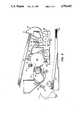
- FIG. 2is an elevational view depicting an electrographic printing machine incorporating the present invention
- FIG. 3a schematic representation of the marking head of the present invention showing the modulation electrodes, the switching elements and the multiplexed driver circuitry;
- FIGS. 4a-4eillustrate vertical line width control and cross-talk elimination in accordance with the present invention.
- FIG. 1a housing 10 which includes an electrically conductive, elongated chamber 12 and a corona discharge wire 14, extending along the length of the chamber.
- a high potential source 16on the order of several thousand volts dc, is connected to the wire 14 through a suitable load resistor 18, and a reference potential source 20 (which may be ground) is connected to the wall of chamber 12.
- a corona dischargesurrounds the wire, creating a source of ions of a given polarity (preferably positive), which are attracted to the grounded chamber wall and fill the chamber with a space charge.
- An inlet channel 22extends along the chamber substantially parallel to wire 14 to deliver pressurized transport fluid (preferably air) into the chamber 12 from a suitable source, schematically illustrated by the tube 24.
- An outlet channel 26, from the chamber 12,also extends substantially parallel to wire 14, at a location opposed to inlet channel 22, for conducting the ion laden transport fluid to the exterior of the housing 10.
- the outlet channel 26comprises two portions, a first portion directed substantially radially outwardly from the chamber and a second portion 30 angularly disposed to the first portion.
- the second portion 30is formed by the unsupported extension of a marking head 32 spaced from and secured to the housing by insulating shim 34.
- the ion laden transport fluidpasses through the outlet 26, it flows over an array of ion pixel or modulation electrodes 36, each extending in the direction of the fluid flow, and integrally formed on the marking head 32.
- An insulating charge receiver 42is interposed between the accelerating back electrode and the housing, and is moved over the back electrode for collecting the ions upon its surface in an image configuration.
- the ions in the transport fluid streammay be viewed as individual “beams", which may be allowed to pass to the receiver 42 or to be suppressed within the outlet channel.
- "Writing" of a single spot in a raster lineis accomplished when the modulation electrode is selectively connected to a potential source at substantially the same potential as that on the opposing wall of the outlet channel. With both walls bridging the channel being at about the same electrical potential, there will be substantially no electrical field extending thereacross. Thus, ions passing therethrough will be unaffected and will exit the housing to be deposited upon the charge receptor.
- An imagewise pattern of informationwill be formed by selectively controlling each of the modulation electrodes in the array so that the ion beams associated therewith either exit or are inhibited from exiting the housing in accordance with the pattern and intensity of light and dark spots of the image to be reproduced.
- the image to be reproducedis generally a digital image and that each light and dark spot is generally represented by a binary 0 or 1.
- a printing apparatusin accordance with the present invention.
- the receiver 42a substrate supporting any suitable electrostatic material is charged to a background voltage, in a preferred embodiment, approximately -1500 volts.
- the receiver 42is rotated in a direction of the arrow passed the outlet channel 26 of the fluid jet assisted ion projection apparatus.
- the charge pattern corresponding to the image to be reproducedis projected onto the surface of the receiver 42 providing a latent image.
- suitable developer rolls 46such as magnetic development rolls advance a developer material into contact with the electrostatic latent image.
- the latentattracts toner particles from the carrier granules of the developer material to form a toner powder image upon the surface of the receiver.
- the receiver 42then advances to a transfer station shown generally at 48 where a copy sheet is moved into contact with the powder image.
- the transfer station 48includes a transfer corotron 50 for spraying ions onto the backside of the copy sheet and also includes a pretransfer baffle generally shown at 52.
- Copy sheetsare fed from selected trays, for example, tray 54 and conveyed through a suitable copy sheet paper path, driven by suitable rolls such as rolls 56 and 58 to the transfer station.
- the copy sheetare driven to a fuser station including fusing rolls for permanently affixing the transferred powder image to the copy sheet.
- the fuser assemblyincludes a heated fuser roll 60 and backup or pressure roll 62 with the sheet passing therebetween.
- the copy sheetis transported to a suitable output tray such as illustrated at 64.
- a suitable cleaner 66for example, a blade cleaner in contact with the receiver surface removes residual particles from the surface.
- an erase scorotron 68neutralizes the charge on the receiver and recharges the receiver to the background voltage.
- the marking head 32comprises the elements schematically illustrated in FIG. 3 supported upon a planar substrate 41 (represented by the dotted outline). These elements include an array of modulation electrodes (E) 36 and a multiplexed data entry or loading circuit, comprising a small number of address bus lines (A) 43 and data bus lines (D) 45. Each of the modulation electrodes in the array is individually switchable while simultaneously reducing the number of wire bonds required to interface the electrodes with the external driver circuits. Thin film switches 47 are fabricated directly on the marking head between the electrodes 36 and the data bus lines 45 connected so that no wire bonds are required.
- the switches 47are preferably amorphous silicon thin film transistors (a-Si:H TFTs), although other materials such as polycrystalline Si, laser annealed Si, CdS, Te, or ZnO may be used.
- a-Si:H TFTsamorphous silicon thin film transistors
- each modulation electrode 36is connected to the drain electrode 49 of the thin film transistor
- an address bus line 43(connected to a strobe voltage) is connected to the gate electrode 51 and a data bus line 45 is connected to a data voltage is connected to source electrode 53. Since the number of address bus lines and data bus lines is reduced to a very small number through a multiplexing scheme, the number of wire bonds required will be kept to a minimum. Wire bonding will be necessary between external IC address bus drivers 57 and the address bus line 43, and between the external IC data bus drivers 55 and the data bus lines 45.
- a low cost marking headincorporates modulation electrodes, thin film switching devices, address and data buses, all integrally fabricated upon a single, inexpensive substrate as shown. It includes a-Si:H TFT switches which, ordinarily, would be discarded out of hand, as switching devices for a high speed printer because of their relatively small current capability, resulting in their relatively slow response time.
- a-Si:H TFT switcheswhich, ordinarily, would be discarded out of hand, as switching devices for a high speed printer because of their relatively small current capability, resulting in their relatively slow response time.
- the fluid jet assisted ion projection electrographic marking apparatusit has been shown that they are uniquely compatible.
- each of the pixel or array modulation electrodes 36receives an electrode voltage from switch 47 that is a function of the strobe voltage at gate electrode 51 and the data voltage at source electrode 53 to the transistor switch 47 for that particular modulation electrode 36. It has been discovered that the vertical black line problem has been caused by the voltage leakage or cross-talk between adjacent modulation electrodes 36 on the electrode array.
- the TFT or switch 47shuts off and no leakage from the modulating electrode 36 back through the switch 47 is allowed.
- the potential difference in the outlet channel 26charges the pixel electrodes 36 positively and the pixel electrode 36 become more positive, for example, 26 volts, than the input data voltages.
- FIG. 4bthere is illustrated the attempt to write a one bit black line, i.e. zero voltage at the source gate 53 of the middle pixel electrode.
- the one bit black line pixel electrodeimmediately goes to zero, but neighboring white pixel electrodes are over modulated at +26 volts as illustrated.
- the white pixel electrodes 36leak voltage to the black pixel electrode as illustrated and overmodulation decreases or is eliminated.
- the data voltageis less than the strobe voltage, illustrated as 20 volts, there is a leakage path through the switch 47 which allows the current causing overmodulation to bleed off leaving the pixel electrode with approximately 16 volts.
- the neighboring white pixel electrodes 36are not overmodulated, i.e. illustrated at 16 volts rather than 26 volts.
- cross-talk or vertical line fade outoccurs in data voltage and strobe voltage set points where the data voltage is approximately equal to the strobe voltage or greater the the strobe voltage.
- this phenomenoncan be avoided. How far below the strobe voltage the data must be set varies from array to array. Arrays require a difference of up to 5 V between strobe and data voltages to eliminate fade in or cross talk. After eliminating fade in further reductions in the data voltage increase the 1 and 2 pixel (and to a lesser degree wider) vertical line widths.
- the lower limit on data voltageis the voltage where ions are not shut off completely.
- the control of the data voltageallows vertical line width to be adjusted to (in conjunction with pixel stretching) to achieve 1 to 1 horizontal to vertical line width ratios.
Landscapes
- Physics & Mathematics (AREA)
- General Physics & Mathematics (AREA)
- Combination Of More Than One Step In Electrophotography (AREA)
- Color Electrophotography (AREA)
- Fax Reproducing Arrangements (AREA)
- Printers Or Recording Devices Using Electromagnetic And Radiation Means (AREA)
- Electrophotography Using Other Than Carlson'S Method (AREA)
Abstract
Description
Claims (8)
Priority Applications (2)
| Application Number | Priority Date | Filing Date | Title |
|---|---|---|---|
| US07/194,238US4794412A (en) | 1988-05-16 | 1988-05-16 | Vertical line width control ionographic system |
| JP1112754AJPH0218590A (en) | 1988-05-16 | 1989-05-01 | Vertical line width control type ionographic system |
Applications Claiming Priority (1)
| Application Number | Priority Date | Filing Date | Title |
|---|---|---|---|
| US07/194,238US4794412A (en) | 1988-05-16 | 1988-05-16 | Vertical line width control ionographic system |
Publications (1)
| Publication Number | Publication Date |
|---|---|
| US4794412Atrue US4794412A (en) | 1988-12-27 |
Family
ID=22716835
Family Applications (1)
| Application Number | Title | Priority Date | Filing Date |
|---|---|---|---|
| US07/194,238Expired - LifetimeUS4794412A (en) | 1988-05-16 | 1988-05-16 | Vertical line width control ionographic system |
Country Status (2)
| Country | Link |
|---|---|
| US (1) | US4794412A (en) |
| JP (1) | JPH0218590A (en) |
Cited By (18)
| Publication number | Priority date | Publication date | Assignee | Title |
|---|---|---|---|---|
| US4958171A (en)* | 1987-05-15 | 1990-09-18 | Sci Systems, Inc. | Printing apparatus and method |
| US5081475A (en)* | 1990-07-30 | 1992-01-14 | Xerox Corporation | Vertical line width control ionographic system |
| US5200770A (en)* | 1991-11-12 | 1993-04-06 | Xerox Corporation | Background from an electrographic printer through modulated off states |
| US5225856A (en)* | 1991-12-23 | 1993-07-06 | Xerox Corporation | Method and apparatus for correction of blooming artifacts in ionographic devices |
| US5270729A (en)* | 1991-06-21 | 1993-12-14 | Xerox Corporation | Ionographic beam positioning and crosstalk correction using grey levels |
| US20060109333A1 (en)* | 2004-11-25 | 2006-05-25 | Oce-Technologies B.V. | Image-forming element for a printing apparatus with a multiplex circuit for driving the image-forming electrodes |
| EP1679560A3 (en)* | 2004-11-25 | 2006-08-02 | Océ-Technologies B.V. | Image-forming element for a printing apparatus with multiplex circuit for driving the image-forming electrodes |
| US11122971B2 (en) | 2016-08-18 | 2021-09-21 | Neptune Medical Inc. | Device and method for enhanced visualization of the small intestine |
| US11135398B2 (en) | 2018-07-19 | 2021-10-05 | Neptune Medical Inc. | Dynamically rigidizing composite medical structures |
| US11219351B2 (en) | 2015-09-03 | 2022-01-11 | Neptune Medical Inc. | Device for endoscopic advancement through the small intestine |
| US11744443B2 (en) | 2020-03-30 | 2023-09-05 | Neptune Medical Inc. | Layered walls for rigidizing devices |
| US11793392B2 (en) | 2019-04-17 | 2023-10-24 | Neptune Medical Inc. | External working channels |
| US11937778B2 (en) | 2022-04-27 | 2024-03-26 | Neptune Medical Inc. | Apparatuses and methods for determining if an endoscope is contaminated |
| US12059128B2 (en) | 2018-05-31 | 2024-08-13 | Neptune Medical Inc. | Device and method for enhanced visualization of the small intestine |
| US12121677B2 (en) | 2021-01-29 | 2024-10-22 | Neptune Medical Inc. | Devices and methods to prevent inadvertent motion of dynamically rigidizing apparatuses |
| US12295550B2 (en) | 2017-07-20 | 2025-05-13 | Neptune Medical Inc. | Dynamically rigidizing overtube |
| US12330292B2 (en) | 2023-09-28 | 2025-06-17 | Neptune Medical Inc. | Telescoping robot |
| US12329473B2 (en) | 2019-04-17 | 2025-06-17 | Neptune Medical Inc. | Dynamically rigidizing composite medical structures |
Citations (4)
| Publication number | Priority date | Publication date | Assignee | Title |
|---|---|---|---|---|
| US4463363A (en)* | 1982-07-06 | 1984-07-31 | Xerox Corporation | Fluid assisted ion projection printing |
| US4558334A (en)* | 1983-06-06 | 1985-12-10 | Fotland Richard A | Electrostatic imaging device |
| US4658275A (en)* | 1984-03-23 | 1987-04-14 | Canon Kabushiki Kaisha | Image forming apparatus |
| US4697196A (en)* | 1985-02-13 | 1987-09-29 | Canon Kabushiki Kaisha | Electrostatic recording method and apparatus |
Family Cites Families (1)
| Publication number | Priority date | Publication date | Assignee | Title |
|---|---|---|---|---|
| US4646163A (en)* | 1985-10-07 | 1987-02-24 | Xerox Corporation | Ion projection copier |
- 1988
- 1988-05-16USUS07/194,238patent/US4794412A/ennot_activeExpired - Lifetime
- 1989
- 1989-05-01JPJP1112754Apatent/JPH0218590A/enactivePending
Patent Citations (4)
| Publication number | Priority date | Publication date | Assignee | Title |
|---|---|---|---|---|
| US4463363A (en)* | 1982-07-06 | 1984-07-31 | Xerox Corporation | Fluid assisted ion projection printing |
| US4558334A (en)* | 1983-06-06 | 1985-12-10 | Fotland Richard A | Electrostatic imaging device |
| US4658275A (en)* | 1984-03-23 | 1987-04-14 | Canon Kabushiki Kaisha | Image forming apparatus |
| US4697196A (en)* | 1985-02-13 | 1987-09-29 | Canon Kabushiki Kaisha | Electrostatic recording method and apparatus |
Cited By (30)
| Publication number | Priority date | Publication date | Assignee | Title |
|---|---|---|---|---|
| US4958171A (en)* | 1987-05-15 | 1990-09-18 | Sci Systems, Inc. | Printing apparatus and method |
| US5081475A (en)* | 1990-07-30 | 1992-01-14 | Xerox Corporation | Vertical line width control ionographic system |
| US5270729A (en)* | 1991-06-21 | 1993-12-14 | Xerox Corporation | Ionographic beam positioning and crosstalk correction using grey levels |
| US5200770A (en)* | 1991-11-12 | 1993-04-06 | Xerox Corporation | Background from an electrographic printer through modulated off states |
| US5225856A (en)* | 1991-12-23 | 1993-07-06 | Xerox Corporation | Method and apparatus for correction of blooming artifacts in ionographic devices |
| EP1679560A3 (en)* | 2004-11-25 | 2006-08-02 | Océ-Technologies B.V. | Image-forming element for a printing apparatus with multiplex circuit for driving the image-forming electrodes |
| US20060109333A1 (en)* | 2004-11-25 | 2006-05-25 | Oce-Technologies B.V. | Image-forming element for a printing apparatus with a multiplex circuit for driving the image-forming electrodes |
| US7548250B2 (en) | 2004-11-25 | 2009-06-16 | Oce-Technologies B.V. | Image-forming element for a printing apparatus with a multiplex circuit for driving the image-forming electrodes |
| US12082776B2 (en) | 2015-09-03 | 2024-09-10 | Neptune Medical Inc. | Methods for advancing a device through a gastrointestinal tract |
| US11219351B2 (en) | 2015-09-03 | 2022-01-11 | Neptune Medical Inc. | Device for endoscopic advancement through the small intestine |
| US11122971B2 (en) | 2016-08-18 | 2021-09-21 | Neptune Medical Inc. | Device and method for enhanced visualization of the small intestine |
| US11944277B2 (en) | 2016-08-18 | 2024-04-02 | Neptune Medical Inc. | Device and method for enhanced visualization of the small intestine |
| US12336695B2 (en) | 2016-08-18 | 2025-06-24 | Neptune Medical Inc. | Device and method for enhanced visualization of the small intestine |
| US12295550B2 (en) | 2017-07-20 | 2025-05-13 | Neptune Medical Inc. | Dynamically rigidizing overtube |
| US12059128B2 (en) | 2018-05-31 | 2024-08-13 | Neptune Medical Inc. | Device and method for enhanced visualization of the small intestine |
| US11724065B2 (en) | 2018-07-19 | 2023-08-15 | Neptune Medical Inc. | Nested rigidizing devices |
| US11554248B1 (en) | 2018-07-19 | 2023-01-17 | Neptune Medical Inc. | Rigidizing devices |
| US11478608B2 (en) | 2018-07-19 | 2022-10-25 | Neptune Medical Inc. | Dynamically rigidizing composite medical structures |
| US11135398B2 (en) | 2018-07-19 | 2021-10-05 | Neptune Medical Inc. | Dynamically rigidizing composite medical structures |
| US12311122B2 (en) | 2018-07-19 | 2025-05-27 | Neptune Medical Inc. | Rigidizing overtube with hemostasis valve |
| US12285571B2 (en) | 2018-07-19 | 2025-04-29 | Neptune Medical Inc. | Methods of performing vascular procedures using a rigidizing device |
| US11793392B2 (en) | 2019-04-17 | 2023-10-24 | Neptune Medical Inc. | External working channels |
| US12329473B2 (en) | 2019-04-17 | 2025-06-17 | Neptune Medical Inc. | Dynamically rigidizing composite medical structures |
| US12193637B2 (en) | 2019-04-17 | 2025-01-14 | Neptune Medical Inc. | External working channels |
| US11744443B2 (en) | 2020-03-30 | 2023-09-05 | Neptune Medical Inc. | Layered walls for rigidizing devices |
| US12121677B2 (en) | 2021-01-29 | 2024-10-22 | Neptune Medical Inc. | Devices and methods to prevent inadvertent motion of dynamically rigidizing apparatuses |
| US12324565B2 (en) | 2022-04-27 | 2025-06-10 | Neptune Medical Inc. | Methods of attaching a rigidizing sheath to an endoscope |
| US12102289B2 (en) | 2022-04-27 | 2024-10-01 | Neptune Medical Inc. | Methods of attaching a rigidizing sheath to an endoscope |
| US11937778B2 (en) | 2022-04-27 | 2024-03-26 | Neptune Medical Inc. | Apparatuses and methods for determining if an endoscope is contaminated |
| US12330292B2 (en) | 2023-09-28 | 2025-06-17 | Neptune Medical Inc. | Telescoping robot |
Also Published As
| Publication number | Publication date |
|---|---|
| JPH0218590A (en) | 1990-01-22 |
Similar Documents
| Publication | Publication Date | Title |
|---|---|---|
| US4794412A (en) | Vertical line width control ionographic system | |
| US4584592A (en) | Marking head for fluid jet assisted ion projection imaging systems | |
| EP0082281B1 (en) | Electrophotographic printer and method of electrophotographic printing | |
| US6100909A (en) | Matrix addressable array for digital xerography | |
| US4830468A (en) | Liquid crystal print bar having a single backplane electrode | |
| US4646163A (en) | Ion projection copier | |
| US4016813A (en) | Electrostatic line printer | |
| US4973994A (en) | Method and apparatus for controlling ion trajectory perturbations in ionographic devices | |
| US4972212A (en) | Method and apparatus for controlling ion trajectory perturbations in ionographic devices | |
| JPH04304475A (en) | Electrostatic-image coloring process | |
| US4839670A (en) | Synchronized aperture motion ionography | |
| US4719481A (en) | Electrographic ion writing head driver system | |
| JP3252973B2 (en) | Image forming device | |
| CA1327834C (en) | Laser addressed ionography | |
| US5081475A (en) | Vertical line width control ionographic system | |
| US5717449A (en) | Toner projection printer with improved address electrode structure | |
| US4468681A (en) | Electrostatic record image forming method | |
| JPH0635370A (en) | Electrophoretic image copying device and electrophoretic image display sheet for holding copied image | |
| US9037020B2 (en) | Image forming apparatus | |
| EP0752318B1 (en) | Toner projection printer with capacitance-coupled address electrode structure | |
| US6056390A (en) | Image forming apparatus wherein the velocity of the toner supporting medium is higher than recording medium transport velocity | |
| US5072243A (en) | Electrostatic purge for an ion projection device | |
| US4654677A (en) | Recording apparatus | |
| US5138349A (en) | Apparatus for reducing the effects of ambient humidity variations upon an ionographic printing device | |
| US6250741B1 (en) | Image forming apparatus using gates and electrodes for selectively passing toner |
Legal Events
| Date | Code | Title | Description |
|---|---|---|---|
| AS | Assignment | Owner name:XEROX CORPORATION, STAMFORD, CT. A CORP. OF NEW YO Free format text:ASSIGNMENT OF ASSIGNORS INTEREST.;ASSIGNORS:CASEY, BRENDAN C.;GARY, WILLIAM L.;REEL/FRAME:004891/0871 Effective date:19880512 Owner name:XEROX CORPORATION, CONNECTICUT Free format text:ASSIGNMENT OF ASSIGNORS INTEREST;ASSIGNORS:CASEY, BRENDAN C.;GARY, WILLIAM L.;REEL/FRAME:004891/0871 Effective date:19880512 | |
| STCF | Information on status: patent grant | Free format text:PATENTED CASE | |
| FPAY | Fee payment | Year of fee payment:4 | |
| FPAY | Fee payment | Year of fee payment:8 | |
| FPAY | Fee payment | Year of fee payment:12 | |
| AS | Assignment | Owner name:BANK ONE, NA, AS ADMINISTRATIVE AGENT, ILLINOIS Free format text:SECURITY INTEREST;ASSIGNOR:XEROX CORPORATION;REEL/FRAME:013153/0001 Effective date:20020621 | |
| AS | Assignment | Owner name:JPMORGAN CHASE BANK, AS COLLATERAL AGENT, TEXAS Free format text:SECURITY AGREEMENT;ASSIGNOR:XEROX CORPORATION;REEL/FRAME:015134/0476 Effective date:20030625 Owner name:JPMORGAN CHASE BANK, AS COLLATERAL AGENT,TEXAS Free format text:SECURITY AGREEMENT;ASSIGNOR:XEROX CORPORATION;REEL/FRAME:015134/0476 Effective date:20030625 | |
| AS | Assignment | Owner name:XEROX CORPORATION, CONNECTICUT Free format text:RELEASE BY SECURED PARTY;ASSIGNOR:JPMORGAN CHASE BANK, N.A. AS SUCCESSOR-IN-INTEREST ADMINISTRATIVE AGENT AND COLLATERAL AGENT TO JPMORGAN CHASE BANK;REEL/FRAME:066728/0193 Effective date:20220822 |