US4793872A - III-V Compound heteroepitaxial 3-D semiconductor structures utilizing superlattices - Google Patents
III-V Compound heteroepitaxial 3-D semiconductor structures utilizing superlatticesDownload PDFInfo
- Publication number
- US4793872A US4793872AUS07/021,684US2168487AUS4793872AUS 4793872 AUS4793872 AUS 4793872AUS 2168487 AUS2168487 AUS 2168487AUS 4793872 AUS4793872 AUS 4793872A
- Authority
- US
- United States
- Prior art keywords
- layers
- lattice parameter
- functional component
- substrate
- semiconductor material
- Prior art date
- Legal status (The legal status is an assumption and is not a legal conclusion. Google has not performed a legal analysis and makes no representation as to the accuracy of the status listed.)
- Expired - Fee Related
Links
- 239000004065semiconductorSubstances0.000titleclaimsabstractdescription33
- 150000001875compoundsChemical class0.000titledescription2
- 239000000463materialSubstances0.000claimsabstractdescription52
- 239000000758substrateSubstances0.000claimsabstractdescription31
- 230000003287optical effectEffects0.000claimsdescription9
- 229910000530Gallium indium arsenideInorganic materials0.000claimsdescription8
- 230000007547defectEffects0.000claimsdescription8
- 239000002902ferrimagnetic materialSubstances0.000claimsdescription7
- ZPDRQAVGXHVGTB-UHFFFAOYSA-Ngallium;gadolinium(3+);oxygen(2-)Chemical compound[O-2].[O-2].[O-2].[Ga+3].[Gd+3]ZPDRQAVGXHVGTB-UHFFFAOYSA-N0.000claimsdescription7
- 230000005291magnetic effectEffects0.000claimsdescription7
- JBRZTFJDHDCESZ-UHFFFAOYSA-NAsGaChemical group[As]#[Ga]JBRZTFJDHDCESZ-UHFFFAOYSA-N0.000claimsdescription4
- 239000013078crystalSubstances0.000claimsdescription4
- 229910001218Gallium arsenideInorganic materials0.000claimsdescription3
- GPXJNWSHGFTCBW-UHFFFAOYSA-NIndium phosphideChemical compound[In]#PGPXJNWSHGFTCBW-UHFFFAOYSA-N0.000claimsdescription3
- 239000002223garnetSubstances0.000claimsdescription2
- MTRJKZUDDJZTLA-UHFFFAOYSA-Niron yttriumChemical compound[Fe].[Y]MTRJKZUDDJZTLA-UHFFFAOYSA-N0.000claimsdescription2
- 238000000034methodMethods0.000description9
- 238000010276constructionMethods0.000description5
- 238000010521absorption reactionMethods0.000description2
- 238000005229chemical vapour depositionMethods0.000description2
- 230000005855radiationEffects0.000description2
- 238000000927vapour-phase epitaxyMethods0.000description2
- GYHNNYVSQQEPJS-UHFFFAOYSA-NGalliumChemical compound[Ga]GYHNNYVSQQEPJS-UHFFFAOYSA-N0.000description1
- 238000009825accumulationMethods0.000description1
- 229910045601alloyInorganic materials0.000description1
- 239000000956alloySubstances0.000description1
- 229910052782aluminiumInorganic materials0.000description1
- XAGFODPZIPBFFR-UHFFFAOYSA-NaluminiumChemical compound[Al]XAGFODPZIPBFFR-UHFFFAOYSA-N0.000description1
- 229910052787antimonyInorganic materials0.000description1
- WATWJIUSRGPENY-UHFFFAOYSA-Nantimony atomChemical compound[Sb]WATWJIUSRGPENY-UHFFFAOYSA-N0.000description1
- 230000015572biosynthetic processEffects0.000description1
- 238000012512characterization methodMethods0.000description1
- 238000010586diagramMethods0.000description1
- 238000000407epitaxyMethods0.000description1
- 229910052733galliumInorganic materials0.000description1
- 239000012535impuritySubstances0.000description1
- 229910052738indiumInorganic materials0.000description1
- APFVFJFRJDLVQX-UHFFFAOYSA-Nindium atomChemical compound[In]APFVFJFRJDLVQX-UHFFFAOYSA-N0.000description1
- 238000004519manufacturing processMethods0.000description1
- 239000000203mixtureSubstances0.000description1
- 230000005693optoelectronicsEffects0.000description1
- 150000002902organometallic compoundsChemical class0.000description1
- 238000000926separation methodMethods0.000description1
- 230000007704transitionEffects0.000description1
Images


Classifications
- H—ELECTRICITY
- H10—SEMICONDUCTOR DEVICES; ELECTRIC SOLID-STATE DEVICES NOT OTHERWISE PROVIDED FOR
- H10D—INORGANIC ELECTRIC SEMICONDUCTOR DEVICES
- H10D84/00—Integrated devices formed in or on semiconductor substrates that comprise only semiconducting layers, e.g. on Si wafers or on GaAs-on-Si wafers
- H10D84/01—Manufacture or treatment
- H10D84/02—Manufacture or treatment characterised by using material-based technologies
- H10D84/03—Manufacture or treatment characterised by using material-based technologies using Group IV technology, e.g. silicon technology or silicon-carbide [SiC] technology
- H10D84/038—Manufacture or treatment characterised by using material-based technologies using Group IV technology, e.g. silicon technology or silicon-carbide [SiC] technology using silicon technology, e.g. SiGe
- H—ELECTRICITY
- H01—ELECTRIC ELEMENTS
- H01L—SEMICONDUCTOR DEVICES NOT COVERED BY CLASS H10
- H01L21/00—Processes or apparatus adapted for the manufacture or treatment of semiconductor or solid state devices or of parts thereof
- H01L21/02—Manufacture or treatment of semiconductor devices or of parts thereof
- H01L21/02104—Forming layers
- H01L21/02365—Forming inorganic semiconducting materials on a substrate
- H01L21/02367—Substrates
- H01L21/0237—Materials
- H—ELECTRICITY
- H01—ELECTRIC ELEMENTS
- H01L—SEMICONDUCTOR DEVICES NOT COVERED BY CLASS H10
- H01L21/00—Processes or apparatus adapted for the manufacture or treatment of semiconductor or solid state devices or of parts thereof
- H01L21/02—Manufacture or treatment of semiconductor devices or of parts thereof
- H01L21/02104—Forming layers
- H01L21/02365—Forming inorganic semiconducting materials on a substrate
- H01L21/02436—Intermediate layers between substrates and deposited layers
- H01L21/02439—Materials
- H01L21/02455—Group 13/15 materials
- H01L21/02461—Phosphides
- H—ELECTRICITY
- H01—ELECTRIC ELEMENTS
- H01L—SEMICONDUCTOR DEVICES NOT COVERED BY CLASS H10
- H01L21/00—Processes or apparatus adapted for the manufacture or treatment of semiconductor or solid state devices or of parts thereof
- H01L21/02—Manufacture or treatment of semiconductor devices or of parts thereof
- H01L21/02104—Forming layers
- H01L21/02365—Forming inorganic semiconducting materials on a substrate
- H01L21/02518—Deposited layers
- H01L21/02521—Materials
- H01L21/02538—Group 13/15 materials
- H01L21/02546—Arsenides
- H—ELECTRICITY
- H10—SEMICONDUCTOR DEVICES; ELECTRIC SOLID-STATE DEVICES NOT OTHERWISE PROVIDED FOR
- H10D—INORGANIC ELECTRIC SEMICONDUCTOR DEVICES
- H10D88/00—Three-dimensional [3D] integrated devices
- H10D88/01—Manufacture or treatment
- Y—GENERAL TAGGING OF NEW TECHNOLOGICAL DEVELOPMENTS; GENERAL TAGGING OF CROSS-SECTIONAL TECHNOLOGIES SPANNING OVER SEVERAL SECTIONS OF THE IPC; TECHNICAL SUBJECTS COVERED BY FORMER USPC CROSS-REFERENCE ART COLLECTIONS [XRACs] AND DIGESTS
- Y10—TECHNICAL SUBJECTS COVERED BY FORMER USPC
- Y10S—TECHNICAL SUBJECTS COVERED BY FORMER USPC CROSS-REFERENCE ART COLLECTIONS [XRACs] AND DIGESTS
- Y10S148/00—Metal treatment
- Y10S148/065—Gp III-V generic compounds-processing
- Y—GENERAL TAGGING OF NEW TECHNOLOGICAL DEVELOPMENTS; GENERAL TAGGING OF CROSS-SECTIONAL TECHNOLOGIES SPANNING OVER SEVERAL SECTIONS OF THE IPC; TECHNICAL SUBJECTS COVERED BY FORMER USPC CROSS-REFERENCE ART COLLECTIONS [XRACs] AND DIGESTS
- Y10—TECHNICAL SUBJECTS COVERED BY FORMER USPC
- Y10S—TECHNICAL SUBJECTS COVERED BY FORMER USPC CROSS-REFERENCE ART COLLECTIONS [XRACs] AND DIGESTS
- Y10S148/00—Metal treatment
- Y10S148/072—Heterojunctions
- Y—GENERAL TAGGING OF NEW TECHNOLOGICAL DEVELOPMENTS; GENERAL TAGGING OF CROSS-SECTIONAL TECHNOLOGIES SPANNING OVER SEVERAL SECTIONS OF THE IPC; TECHNICAL SUBJECTS COVERED BY FORMER USPC CROSS-REFERENCE ART COLLECTIONS [XRACs] AND DIGESTS
- Y10—TECHNICAL SUBJECTS COVERED BY FORMER USPC
- Y10S—TECHNICAL SUBJECTS COVERED BY FORMER USPC CROSS-REFERENCE ART COLLECTIONS [XRACs] AND DIGESTS
- Y10S148/00—Metal treatment
- Y10S148/097—Lattice strain and defects
- Y—GENERAL TAGGING OF NEW TECHNOLOGICAL DEVELOPMENTS; GENERAL TAGGING OF CROSS-SECTIONAL TECHNOLOGIES SPANNING OVER SEVERAL SECTIONS OF THE IPC; TECHNICAL SUBJECTS COVERED BY FORMER USPC CROSS-REFERENCE ART COLLECTIONS [XRACs] AND DIGESTS
- Y10—TECHNICAL SUBJECTS COVERED BY FORMER USPC
- Y10S—TECHNICAL SUBJECTS COVERED BY FORMER USPC CROSS-REFERENCE ART COLLECTIONS [XRACs] AND DIGESTS
- Y10S148/00—Metal treatment
- Y10S148/11—Metal-organic CVD, ruehrwein type
- Y—GENERAL TAGGING OF NEW TECHNOLOGICAL DEVELOPMENTS; GENERAL TAGGING OF CROSS-SECTIONAL TECHNOLOGIES SPANNING OVER SEVERAL SECTIONS OF THE IPC; TECHNICAL SUBJECTS COVERED BY FORMER USPC CROSS-REFERENCE ART COLLECTIONS [XRACs] AND DIGESTS
- Y10—TECHNICAL SUBJECTS COVERED BY FORMER USPC
- Y10S—TECHNICAL SUBJECTS COVERED BY FORMER USPC CROSS-REFERENCE ART COLLECTIONS [XRACs] AND DIGESTS
- Y10S148/00—Metal treatment
- Y10S148/16—Superlattice
- Y—GENERAL TAGGING OF NEW TECHNOLOGICAL DEVELOPMENTS; GENERAL TAGGING OF CROSS-SECTIONAL TECHNOLOGIES SPANNING OVER SEVERAL SECTIONS OF THE IPC; TECHNICAL SUBJECTS COVERED BY FORMER USPC CROSS-REFERENCE ART COLLECTIONS [XRACs] AND DIGESTS
- Y10—TECHNICAL SUBJECTS COVERED BY FORMER USPC
- Y10S—TECHNICAL SUBJECTS COVERED BY FORMER USPC CROSS-REFERENCE ART COLLECTIONS [XRACs] AND DIGESTS
- Y10S148/00—Metal treatment
- Y10S148/164—Three dimensional processing
- Y—GENERAL TAGGING OF NEW TECHNOLOGICAL DEVELOPMENTS; GENERAL TAGGING OF CROSS-SECTIONAL TECHNOLOGIES SPANNING OVER SEVERAL SECTIONS OF THE IPC; TECHNICAL SUBJECTS COVERED BY FORMER USPC CROSS-REFERENCE ART COLLECTIONS [XRACs] AND DIGESTS
- Y10—TECHNICAL SUBJECTS COVERED BY FORMER USPC
- Y10S—TECHNICAL SUBJECTS COVERED BY FORMER USPC CROSS-REFERENCE ART COLLECTIONS [XRACs] AND DIGESTS
- Y10S438/00—Semiconductor device manufacturing: process
- Y10S438/938—Lattice strain control or utilization
- Y—GENERAL TAGGING OF NEW TECHNOLOGICAL DEVELOPMENTS; GENERAL TAGGING OF CROSS-SECTIONAL TECHNOLOGIES SPANNING OVER SEVERAL SECTIONS OF THE IPC; TECHNICAL SUBJECTS COVERED BY FORMER USPC CROSS-REFERENCE ART COLLECTIONS [XRACs] AND DIGESTS
- Y10—TECHNICAL SUBJECTS COVERED BY FORMER USPC
- Y10S—TECHNICAL SUBJECTS COVERED BY FORMER USPC CROSS-REFERENCE ART COLLECTIONS [XRACs] AND DIGESTS
- Y10S438/00—Semiconductor device manufacturing: process
- Y10S438/967—Semiconductor on specified insulator
Definitions
- This inventionrelates to a component of semiconductor material deposited by epitaxial growth on a substrate having a different lattice parameter (lattice constant).
- the inventionis also concerned with the application of said material to a wide range of semiconductor components such as diodes, photoresistors, integrated optical waveguides, optical isolators, optical circulators, magnetic detectors.
- the inventionis applicable in particular to a component of III-V compound material implanted into a substrate.
- 11th, 1984offered a solution by proposing by way of example a semiconductor material composition having a base of gallium, indium, aluminum and antimony (GaInAlSb) in which the lattice parameter of 6.19 ⁇ ngstroms is substantially adjusted to one-half the lattice parameter of the gadolinium-gallium garnet.
- GaInAlSbgallium, indium, aluminum and antimony
- the inventionprovides a component which is easier to produce and accordingly overcomes the disadvantages just mentioned.
- the inventionemploys a known method of epitaxial growth of a succession of layers.
- This methodcalls for the use of a recent epitaxial growth technique of vapor-phase epitaxy known as metal-organic chemical vapor deposition (MOCVD).
- MOCVDmetal-organic chemical vapor deposition
- the succession of layers obtained by means of this methodis known as a superlattice and is described in the article entitled “Growth and characterization of GaInAsInP heterojunction and quantum-well structures obtained by MOCVD" by Manijeh Razeghi, published in the Thomson-CSF Technical Review (Revue Technique), Vol. 16--No.
- the component obtainedhas the advantage of remaining undisturbed by any faults arising from dislocations at the component-substrate interface and is provided in the form of a single crystal.
- the inventionaccordingly relates to a component of semiconductor material deposited by epitaxial growth on a substrate having a predetermined and different lattice parameter, there being formed on said substrate an alternate succession of layers of a first type and layers of a second type as well as a component formed on said succession of layers.
- the layers of the first typeare formed of a first semiconductor material having a lattice parameter which is substantially matched with a multiple or a sub-multiple of the substrate lattice parameter.
- the layers of the second typeare formed of a second semiconductor material having a lattice parameter which is matched with a multiple or a sub-multiple of the lattice parameter of the first material of the layers of the first type.
- the componentis formed of material having the same lattice parameter as the second semiconductor material.
- the layers of the first type and the layers of the second typehave different energy gaps.
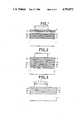
- FIG. 1illustrates one example of construction of the component in accordance with the invention.
- FIG. 2is an explanatory diagram of operation of the component in accordance with the invention.
- FIG. 3illustrates an example of construction of a photoresistor in accordance with the invention.
- FIG. 4illustrates an example of construction of an integrated isolator in accordance with the invention.
- FIG. 5illustrates an example of construction of a magnetic detector in accordance with the invention.
- FIG. 6illustrates an alternative embodiment of the invention in which provision is made for a plurality of superlattices.
- FIG. 1one example of construction in accordance with the invention will now be described.
- a succession of layers M1 to Mi and N1 to Niis grown on a substrate 1.
- the substrateis of semiconductor material such as, for example, gallium arsenide (GaAs) or a gadolinium-gallium garnet (GGG).
- GaAsgallium arsenide
- GGGgadolinium-gallium garnet
- the substratecan also be of ferroelectric material and more generally of any material on which a semiconductor component is to be grown.
- the layers M1, M2, . . . Miare formed with semiconductor material having a lattice parameter a2 which is substantially matched with a multiple or submultiple of the lattice parameter a1 of the substrate.
- the layers N1, N2, . . . Niare formed with semiconductor material having a lattice parameter a3 which is matched with the lattice parameter a2 of the layers M1, M2, . . . Mi.
- the layers M1, M2, . . . Mihave energy gaps which are distinctly different from the energy gaps of the layers N1, N2, . . . Ni.
- the electron affinity of the layers M1 to M2will be very different from the electron affinity of the layers N1 to Ni.
- a spatial separation between electrons and impuritiesis accordingly observed, thus forming a high-density accumulation layer.
- the crystal dissymmetries between the substrate 1 and the layer M1 and the difference in lattice parametersproduce dislocation defects caused by mismatching of crystal lattice parameters between the substrate and the first epitaxial layer.
- each transition between a layer M and a layer Nproduces a deviation of the dislocation angle. As indicated by arrows in FIG. 2, absorption of defects therefore takes place at each interface between a layer N and a layer M.
- the component Cis formed of semiconductor material, the lattice parameter of which is matched with the lattice parameter a3 of the layer Ni and is even equal to the lattice parameter a3.
- the present inventionapplies to a wide range of different components made of semiconductor materials and including, for example, diodes, lasers, waveguides, integrated transistors, optical isolators and optical detectors.
- FIG. 3illustrates a photoresistor in which the component C is made of gallium-indium arsenide (GaInAs) and having electrical characteristics (impedances) which vary under the action of radiation having a wavelength within the range of 1.3 micrometers to 1.5 micrometers.
- the top portion of the photoresistorhas two electrodes which provide electrical connections from the photoresistor to the utilization circuits.
- the top face of the photoresistorsis illuminated by a radiation F having a wavelength which is detectable by the photoresistor.
- the photoresistor Cis of GaInAs and is constructed in a succession of layers M1 to M3 and N1 to N3 which are formed on a substrate 1 of gallium arsenide.
- the layers M1 to M3are of indium phosphide.
- the layers N1 to N3are of gallium-indium arsenide.
- Said photoresistor Ccan be fabricated from another material which is sensitive to different wavelengths as explained earlier. It will be necessary in such a case to choose intermediate layers M1 to M3 and N1 to N3 which permit good attenuation of defects.
- FIG. 4illustrates an integrated isolator as described in French patent application No. 84 18928 filed on Dec. 11th, 1984.
- This isolatoris formed by a layer 1 of ferrimagnetic material such as an yttrium-iron garnet (YIG) on a gadolinium-gallium garnet substrate S.
- YIGyttrium-iron garnet
- This ferrimagnetic materialhas a lattice parameter which provides suitable matching with the gadolinium-gallium garnet substrate S.
- a zone 3 of the layer 1has been machined and carries an emitting diode C.
- the other zone of the layer 1has a waveguide which is machined in the YIG layer.
- the dimensions (L, b) of the waveguideare such that the light emitted by the diode C cannot be reflected back to the diode and disturb its operation, hence the term "integrated isolator" which is used to designate this waveguide.
- the diode Cis fabricated on the YIG layer 1 after formation of a succession of layers M, N constituting a superlattice.
- the layers M and Nwill be formed as described earlier by means of III-V materials chosen as a function of their lattice parameter and energy gap.
- FIG. 5is an illustration of a magnetic detector for a linear magnetoresistive-effect transducer.
- This transduceris mainly constituted by a layer C of semiconductor material, one face of which carries a layer 1 of ferrimagnetic material and the other face of which carries at least one pair of electrodes 4 disposed along an axis OX.
- the transducer under considerationis so arranged that its layer 1 of ferrimagnetic material is placed in proximity to a magnetic support 8 to be read in such a manner as to ensure that a magnetic item of information 70 to 72 induces a magnetic field within the layer C of semiconductor material in a direction OY at right angles to the axis OX of the pair of electrodes.
- the layer C of semiconductor materialshould be matched with the layer 1 of ferrimagnetic material.
- a succession of stacked superlattices of the type described in the foregoingfor example, a first superlattice M1-Mi, N1-Ni is formed on a substrate 1 as illustrated in FIG. 6 and makes it possible to fabricate a first component C1.
- a second component C2having a nature which differs from that of said component C1
- a second superlattice P1-Pj, Q1-Qjis formed on the component C1.
- the nature on the one hand of the layers P1-Pj and on the other hand of the layers Q1-Qjis chosen as a function of their lattice parameters and energy gaps as already described in the case of the layers M1-Mi, N1-Ni. It is thus possible to form a component C2 on the component C1. As can readily be understood, a plurality of components such as C2 may accordingly be formed on the component C1.
- the lattice parameter of the layers M1-Miis substantially matched with the multiple or sub-multiple of the lattice parameter of the component C1.
- this lattice parameteris matched and even equal to the lattice parameter of the layers M1-Mi.
- the lattice parameter of the component C2is equal to the lattice parameter of the layers N1-Ni.
- the inventionis applicable to components employed in the field of optoelectronics as well as the field of optical telecommunications or microwave techniques.
Landscapes
- Engineering & Computer Science (AREA)
- Physics & Mathematics (AREA)
- Condensed Matter Physics & Semiconductors (AREA)
- General Physics & Mathematics (AREA)
- Manufacturing & Machinery (AREA)
- Computer Hardware Design (AREA)
- Microelectronics & Electronic Packaging (AREA)
- Power Engineering (AREA)
- Chemical & Material Sciences (AREA)
- Materials Engineering (AREA)
- Recrystallisation Techniques (AREA)
- Light Receiving Elements (AREA)
- Crystals, And After-Treatments Of Crystals (AREA)
- Semiconductor Lasers (AREA)
- Led Devices (AREA)
- Optical Integrated Circuits (AREA)
Abstract
Description
1. Field of the Invention
This invention relates to a component of semiconductor material deposited by epitaxial growth on a substrate having a different lattice parameter (lattice constant). The invention is also concerned with the application of said material to a wide range of semiconductor components such as diodes, photoresistors, integrated optical waveguides, optical isolators, optical circulators, magnetic detectors.
The invention is applicable in particular to a component of III-V compound material implanted into a substrate.
2. Description of the Prior Art
The fabrication of a component of this type is often difficult in practice since it is necessary to choose semiconductor material having a lattice parameter which is matched with the lattice parameter of the substrate. Thus the lattice parameter of a substrate of gadolinium-gallium garnet and having a value of 12.383 Ångstroms is totally mismatched with respect to known semiconductor materials. In the field of light emitting and receiving diodes, French patent application No. 84 18928 filed on Dec. 11th, 1984 offered a solution by proposing by way of example a semiconductor material composition having a base of gallium, indium, aluminum and antimony (GaInAlSb) in which the lattice parameter of 6.19 Ångstroms is substantially adjusted to one-half the lattice parameter of the gadolinium-gallium garnet.
However, adjustment of the lattice parameters to a multiple or a sub-multiple of the substrate lattice parameter calls for highly accurate dosing of the different metal-organic compounds employed. Furthermore, this dosing operation presupposes that the material has non-tailorable properties, that is, predetermined characteristics which could be determining factors in regard to the field of application.
The invention provides a component which is easier to produce and accordingly overcomes the disadvantages just mentioned.
To this end, the invention employs a known method of epitaxial growth of a succession of layers. This method calls for the use of a recent epitaxial growth technique of vapor-phase epitaxy known as metal-organic chemical vapor deposition (MOCVD). The succession of layers obtained by means of this method is known as a superlattice and is described in the article entitled "Growth and characterization of GaInAsInP heterojunction and quantum-well structures obtained by MOCVD" by Manijeh Razeghi, published in the Thomson-CSF Technical Review (Revue Technique), Vol. 16--No. 1--March 1984,pages 5 to 27, as well as inChapter 5 entitled "Low-pressure metallo-organic chemical vapor deposition of Gax Inb1-x Asy P1-y alloys" by Manijeh Razeghi (paragraph IV, pages 317 to 345) published in the work entitled ∓Semiconductors and semimetals", Vol. 22, part A by Bell Telephone Laboratories.
The component obtained has the advantage of remaining undisturbed by any faults arising from dislocations at the component-substrate interface and is provided in the form of a single crystal.
The invention accordingly relates to a component of semiconductor material deposited by epitaxial growth on a substrate having a predetermined and different lattice parameter, there being formed on said substrate an alternate succession of layers of a first type and layers of a second type as well as a component formed on said succession of layers. The layers of the first type are formed of a first semiconductor material having a lattice parameter which is substantially matched with a multiple or a sub-multiple of the substrate lattice parameter. The layers of the second type are formed of a second semiconductor material having a lattice parameter which is matched with a multiple or a sub-multiple of the lattice parameter of the first material of the layers of the first type. The component is formed of material having the same lattice parameter as the second semiconductor material. The layers of the first type and the layers of the second type have different energy gaps.
FIG. 1 illustrates one example of construction of the component in accordance with the invention.
FIG. 2 is an explanatory diagram of operation of the component in accordance with the invention.
FIG. 3 illustrates an example of construction of a photoresistor in accordance with the invention.
FIG. 4 illustrates an example of construction of an integrated isolator in accordance with the invention.
FIG. 5 illustrates an example of construction of a magnetic detector in accordance with the invention.
FIG. 6 illustrates an alternative embodiment of the invention in which provision is made for a plurality of superlattices.
Referring first to FIG. 1, one example of construction in accordance with the invention will now be described.
A succession of layers M1 to Mi and N1 to Ni is grown on asubstrate 1.
The substrate is of semiconductor material such as, for example, gallium arsenide (GaAs) or a gadolinium-gallium garnet (GGG). The substrate can also be of ferroelectric material and more generally of any material on which a semiconductor component is to be grown.
The layers M1, M2, . . . Mi are formed with semiconductor material having a lattice parameter a2 which is substantially matched with a multiple or submultiple of the lattice parameter a1 of the substrate.
The layers N1, N2, . . . Ni are formed with semiconductor material having a lattice parameter a3 which is matched with the lattice parameter a2 of the layers M1, M2, . . . Mi.
The layers M1, M2, . . . Mi have energy gaps which are distinctly different from the energy gaps of the layers N1, N2, . . . Ni. In consequence, the electron affinity of the layers M1 to M2 will be very different from the electron affinity of the layers N1 to Ni. At the interface between each layer N and the layer M which is superposed thereon, a spatial separation between electrons and impurities is accordingly observed, thus forming a high-density accumulation layer.
The crystal dissymmetries between thesubstrate 1 and the layer M1 and the difference in lattice parameters produce dislocation defects caused by mismatching of crystal lattice parameters between the substrate and the first epitaxial layer. In order to remove these defects, each transition between a layer M and a layer N produces a deviation of the dislocation angle. As indicated by arrows in FIG. 2, absorption of defects therefore takes place at each interface between a layer N and a layer M.
By providing a sufficient number of layers, there is thus obtained an attenuation of defects which does not reach the component C.
By way of example in the case of layers having a thickness of 50 to 150 Ångstroms and with a total of approximately twenty layers, good absorption of defects is accordingly obtained.
The component C is formed of semiconductor material, the lattice parameter of which is matched with the lattice parameter a3 of the layer Ni and is even equal to the lattice parameter a3.
Growth of the different layers and of the component C is performed by epitaxy in accordance with a method known as vapor-phase epitaxy as described in particular in the documents mentioned earlier.
The present invention applies to a wide range of different components made of semiconductor materials and including, for example, diodes, lasers, waveguides, integrated transistors, optical isolators and optical detectors.
By way of example of practical application of the invention, FIG. 3 illustrates a photoresistor in which the component C is made of gallium-indium arsenide (GaInAs) and having electrical characteristics (impedances) which vary under the action of radiation having a wavelength within the range of 1.3 micrometers to 1.5 micrometers. The top portion of the photoresistor has two electrodes which provide electrical connections from the photoresistor to the utilization circuits. Furthermore, the top face of the photoresistors is illuminated by a radiation F having a wavelength which is detectable by the photoresistor.
The photoresistor C is of GaInAs and is constructed in a succession of layers M1 to M3 and N1 to N3 which are formed on asubstrate 1 of gallium arsenide. The layers M1 to M3 are of indium phosphide. The layers N1 to N3 are of gallium-indium arsenide.
Said photoresistor C can be fabricated from another material which is sensitive to different wavelengths as explained earlier. It will be necessary in such a case to choose intermediate layers M1 to M3 and N1 to N3 which permit good attenuation of defects.
FIG. 4 illustrates an integrated isolator as described in French patent application No. 84 18928 filed on Dec. 11th, 1984. This isolator is formed by alayer 1 of ferrimagnetic material such as an yttrium-iron garnet (YIG) on a gadolinium-gallium garnet substrate S. This ferrimagnetic material has a lattice parameter which provides suitable matching with the gadolinium-gallium garnet substrate S.
Azone 3 of thelayer 1 has been machined and carries an emitting diode C. The other zone of thelayer 1 has a waveguide which is machined in the YIG layer. The dimensions (L, b) of the waveguide are such that the light emitted by the diode C cannot be reflected back to the diode and disturb its operation, hence the term "integrated isolator" which is used to designate this waveguide.
The diode C is fabricated on theYIG layer 1 after formation of a succession of layers M, N constituting a superlattice. The layers M and N will be formed as described earlier by means of III-V materials chosen as a function of their lattice parameter and energy gap.
Using the same technique as the isolator considered above, it is possible to construct a circulator which applies the invention by providing a plurality of emitting and receiving diodes connected together in pairs by means of the aforesaid isolators which are formed on the same substrate.
FIG. 5 is an illustration of a magnetic detector for a linear magnetoresistive-effect transducer. This transducer is mainly constituted by a layer C of semiconductor material, one face of which carries alayer 1 of ferrimagnetic material and the other face of which carries at least one pair of electrodes 4 disposed along an axis OX.
The transducer under consideration is so arranged that itslayer 1 of ferrimagnetic material is placed in proximity to a magnetic support 8 to be read in such a manner as to ensure that a magnetic item ofinformation 70 to 72 induces a magnetic field within the layer C of semiconductor material in a direction OY at right angles to the axis OX of the pair of electrodes.
In order to ensure correct operation of a transducer of this type, the layer C of semiconductor material should be matched with thelayer 1 of ferrimagnetic material. By providing a superlattice consisting of a succession of layers M, N, an effective method is thus made available for guarding against any danger of lattice-mismatch defects.
As explained earlier, the invention is applicable to other types of components without thereby departing either from the scope or the spirit of the invention.
In an alternative embodiment of the invention, provision is made for a succession of stacked superlattices of the type described in the foregoing. For example, a first superlattice M1-Mi, N1-Ni is formed on asubstrate 1 as illustrated in FIG. 6 and makes it possible to fabricate a first component C1. In order to form on the component C1 a second component C2 having a nature which differs from that of said component C1, a second superlattice P1-Pj, Q1-Qj is formed on the component C1. The nature on the one hand of the layers P1-Pj and on the other hand of the layers Q1-Qj is chosen as a function of their lattice parameters and energy gaps as already described in the case of the layers M1-Mi, N1-Ni. It is thus possible to form a component C2 on the component C1. As can readily be understood, a plurality of components such as C2 may accordingly be formed on the component C1.
As described in connection with the first superlattice M1-Mi, N1-Ni, the lattice parameter of the layers M1-Mi is substantially matched with the multiple or sub-multiple of the lattice parameter of the component C1. In the case of the layers N1-Ni, this lattice parameter is matched and even equal to the lattice parameter of the layers M1-Mi. The lattice parameter of the component C2 is equal to the lattice parameter of the layers N1-Ni.
Similarly, it would not constitute any departure from the scope of the invention to make provision for one or a number of components (not shown in the figure) which are formed on a component as designated by the reference C2 by means of another superlattice which permits lattice-matching.
The invention is applicable to components employed in the field of optoelectronics as well as the field of optical telecommunications or microwave techniques.
Claims (17)
1. A device formed of semiconductor material deposited by epitaxial growth on a substrate having a predetermined and different lattice parameter, comprising on said substrate an alternate succession of layers of a first semiconductor material ranging in number (i) from 1 to n and layers of a second type ranging in number (i) from 1 to n as well as at least a first functional component for performing a predetermined function formed on said succession of layers, the layers of the first semiconductor material having a lattice parameter which is substantially matched with a multiple or a sub-multiple of the substrate lattice parameter, the layers of the second semiconductor material having a lattice parameter which is matched with a multiple or a sub-multiple of the lattice parameter of the first material, the functional component being formed of material having the same lattice parameter as the second semiconductor material, the energy gaps of the layers of the first semiconductor materials being different;
wherein said alternate succession of layers of said first and second semiconductor materials has interfaces which absorb dislocation defects caused by mismatching of crystal lattice parameters between the substrate and the first semiconductor material;
said device further comprising on said first functional component a second alternate succession of layers of a third semiconductor material and layers of a fourth semiconductor material as well as at least a second functional component formed on said second succession of layers, the lattice parameter of said third material being substantially matched with a multiple or sub-multiple of the lattice parameter of the material of the first functional component, the lattice parameter of the fourth material being matched with a multiple or sub-multiple of the lattice parameter of the third material, the lattice parameter of the second functional component being matched with the lattice parameter of the fourth material of the fourth layer.
2. A device according to claim 1, wherein the second semiconductor material has a lattice parameter which is equal to the lattice parameter of the first semiconductor material.
3. A device according to claim 1, wherein the substrate is a gadolinium-gallium garnet, the first material is indium phosphide (InP), said second material is gallium-indium arsenide (GaInAs).
4. A device according to claim 1, wherein the substrate is of ferrimagnetic material.
5. A device according to claim 1, wherein the substrate is gallium arsenide.
6. A device according to claim 4, wherein the ferrimagnetic material is yttrium-iron garnet (YIG).
7. A device according to claim 1, wherein the thickness of each layer is approximately 50 Ångstroms to 150 Ångstroms.
8. A device according to claim 1, wherein the number of layers is greater than ten layers.
9. A device according to claim 1, wherein the functional component is a laser diode.
10. A device according to claim 1, wherein the functional component is a photoresistor.
11. A device according to claim 1, wherein the functional component is an integrated optical waveguide.
12. A device according to claim 1, wherein the functional component is an integrated optical isolator.
13. A device according to claim 1, wherein the functional component is an optical circulator.
14. A component according to claim 3, wherein the component is a magnetic detector.
15. A device according to claim 1, wherein the first functional component is a photoresistor of gallium-indium arsenide formed on a substrate of gallium arsenide, the alternate succession of layers of the first material and layers of the second material being formed of indium phosphide in the case of the first material and of gallium-indium arsenide in the case of the second material.
16. A device according to claim 1, comprising a plurality of functional components including the second functional component formed on the second alternate succession of layers of the third and fourth materials.
17. A device according to claim 1 wherein a plurality of successions of layers are formed on the second functional component in order to integrate further functional components.
Applications Claiming Priority (2)
| Application Number | Priority Date | Filing Date | Title |
|---|---|---|---|
| FR8603285 | 1986-03-07 | ||
| FR8603285AFR2595509B1 (en) | 1986-03-07 | 1986-03-07 | COMPONENT IN SEMICONDUCTOR MATERIAL EPITAXIA ON A SUBSTRATE WITH DIFFERENT MESH PARAMETER AND APPLICATION TO VARIOUS SEMICONDUCTOR COMPONENTS |
Publications (1)
| Publication Number | Publication Date |
|---|---|
| US4793872Atrue US4793872A (en) | 1988-12-27 |
Family
ID=9332899
Family Applications (1)
| Application Number | Title | Priority Date | Filing Date |
|---|---|---|---|
| US07/021,684Expired - Fee RelatedUS4793872A (en) | 1986-03-07 | 1987-03-04 | III-V Compound heteroepitaxial 3-D semiconductor structures utilizing superlattices |
Country Status (5)
| Country | Link |
|---|---|
| US (1) | US4793872A (en) |
| EP (1) | EP0237413B1 (en) |
| JP (1) | JPS62212619A (en) |
| DE (1) | DE3769816D1 (en) |
| FR (1) | FR2595509B1 (en) |
Cited By (57)
| Publication number | Priority date | Publication date | Assignee | Title |
|---|---|---|---|---|
| US4926226A (en)* | 1988-09-06 | 1990-05-15 | General Motors Corporation | Magnetic field sensors |
| US4927471A (en)* | 1988-03-01 | 1990-05-22 | Fujitsu Limited | Semiconductor substrate comprising wafer substrate and compound semiconductor layer |
| US5099357A (en)* | 1988-08-24 | 1992-03-24 | Matsushita Electric Industrial Co., Ltd. | Optical sensor |
| US5178718A (en)* | 1990-04-24 | 1993-01-12 | U.S. Philips Corporation | Method of manufacturing a semiconductor device |
| US5213906A (en)* | 1989-04-13 | 1993-05-25 | Etat Francais | Composite material comprising a layer of a iii-v compound and a layer of rare earth pnictide, production process and application |
| US5410178A (en)* | 1994-08-22 | 1995-04-25 | Northwestern University | Semiconductor films |
| US5421910A (en)* | 1994-02-10 | 1995-06-06 | Northwestern University | Intermetallic compound semiconductor thin film |
| US5563331A (en)* | 1993-09-29 | 1996-10-08 | Siemens Aktiengesellschaft | Magnetoresistive sensor utilizing a sensor material with a perovskite-like crystal structure |
| US5650635A (en)* | 1995-07-14 | 1997-07-22 | Northwestern University | Multiple stacked Sb-based heterostructures |
| DE19604348A1 (en)* | 1996-02-07 | 1997-08-14 | Deutsche Telekom Ag | Process for the production and calibration of a length scale in the nanometer range for technical devices used for high-resolution or ultra-high-resolution imaging of structures |
| US5668395A (en)* | 1994-11-22 | 1997-09-16 | Northwestern University | Composition for InSB and GaAs thin film on silicon substrate for use in photodetectors |
| US5825057A (en)* | 1991-02-25 | 1998-10-20 | Symetrix Corporation | Process for fabricating layered superlattice materials and making electronic devices including same |
| US6392257B1 (en) | 2000-02-10 | 2002-05-21 | Motorola Inc. | Semiconductor structure, semiconductor device, communicating device, integrated circuit, and process for fabricating the same |
| US6410941B1 (en) | 2000-06-30 | 2002-06-25 | Motorola, Inc. | Reconfigurable systems using hybrid integrated circuits with optical ports |
| US6427066B1 (en) | 2000-06-30 | 2002-07-30 | Motorola, Inc. | Apparatus and method for effecting communications among a plurality of remote stations |
| US6462360B1 (en) | 2001-08-06 | 2002-10-08 | Motorola, Inc. | Integrated gallium arsenide communications systems |
| US6472694B1 (en) | 2001-07-23 | 2002-10-29 | Motorola, Inc. | Microprocessor structure having a compound semiconductor layer |
| WO2002086201A1 (en)* | 2001-04-19 | 2002-10-31 | Motorola, Inc., A Corporation Of The State Of Delaware | Semiconductor structures and devices utilizing perovskite stacks |
| US6477285B1 (en) | 2000-06-30 | 2002-11-05 | Motorola, Inc. | Integrated circuits with optical signal propagation |
| US6501973B1 (en) | 2000-06-30 | 2002-12-31 | Motorola, Inc. | Apparatus and method for measuring selected physical condition of an animate subject |
| US6555946B1 (en) | 2000-07-24 | 2003-04-29 | Motorola, Inc. | Acoustic wave device and process for forming the same |
| WO2003001564A3 (en)* | 2001-06-20 | 2003-05-01 | Motorola Inc | Semiconductor structure with a superlattice portion |
| US6563118B2 (en) | 2000-12-08 | 2003-05-13 | Motorola, Inc. | Pyroelectric device on a monocrystalline semiconductor substrate and process for fabricating same |
| US6583034B2 (en) | 2000-11-22 | 2003-06-24 | Motorola, Inc. | Semiconductor structure including a compliant substrate having a graded monocrystalline layer and methods for fabricating the structure and semiconductor devices including the structure |
| US6585424B2 (en) | 2001-07-25 | 2003-07-01 | Motorola, Inc. | Structure and method for fabricating an electro-rheological lens |
| US6589856B2 (en) | 2001-08-06 | 2003-07-08 | Motorola, Inc. | Method and apparatus for controlling anti-phase domains in semiconductor structures and devices |
| US6594414B2 (en) | 2001-07-25 | 2003-07-15 | Motorola, Inc. | Structure and method of fabrication for an optical switch |
| US6639249B2 (en) | 2001-08-06 | 2003-10-28 | Motorola, Inc. | Structure and method for fabrication for a solid-state lighting device |
| US6638838B1 (en) | 2000-10-02 | 2003-10-28 | Motorola, Inc. | Semiconductor structure including a partially annealed layer and method of forming the same |
| US6646293B2 (en) | 2001-07-18 | 2003-11-11 | Motorola, Inc. | Structure for fabricating high electron mobility transistors utilizing the formation of complaint substrates |
| US6667196B2 (en) | 2001-07-25 | 2003-12-23 | Motorola, Inc. | Method for real-time monitoring and controlling perovskite oxide film growth and semiconductor structure formed using the method |
| US6673667B2 (en) | 2001-08-15 | 2004-01-06 | Motorola, Inc. | Method for manufacturing a substantially integral monolithic apparatus including a plurality of semiconductor materials |
| US6673646B2 (en) | 2001-02-28 | 2004-01-06 | Motorola, Inc. | Growth of compound semiconductor structures on patterned oxide films and process for fabricating same |
| US6693298B2 (en) | 2001-07-20 | 2004-02-17 | Motorola, Inc. | Structure and method for fabricating epitaxial semiconductor on insulator (SOI) structures and devices utilizing the formation of a compliant substrate for materials used to form same |
| US6693033B2 (en) | 2000-02-10 | 2004-02-17 | Motorola, Inc. | Method of removing an amorphous oxide from a monocrystalline surface |
| US6709989B2 (en) | 2001-06-21 | 2004-03-23 | Motorola, Inc. | Method for fabricating a semiconductor structure including a metal oxide interface with silicon |
| US20040171238A1 (en)* | 2003-01-24 | 2004-09-02 | Arena Chantal J. | Enhanced selectivity for epitaxial deposition |
| US20040217444A1 (en)* | 2001-10-17 | 2004-11-04 | Motorola, Inc. | Method and apparatus utilizing monocrystalline insulator |
| US6855992B2 (en) | 2001-07-24 | 2005-02-15 | Motorola Inc. | Structure and method for fabricating configurable transistor devices utilizing the formation of a compliant substrate for materials used to form the same |
| US6885065B2 (en) | 2002-11-20 | 2005-04-26 | Freescale Semiconductor, Inc. | Ferromagnetic semiconductor structure and method for forming the same |
| US6916717B2 (en) | 2002-05-03 | 2005-07-12 | Motorola, Inc. | Method for growing a monocrystalline oxide layer and for fabricating a semiconductor device on a monocrystalline substrate |
| US6965128B2 (en) | 2003-02-03 | 2005-11-15 | Freescale Semiconductor, Inc. | Structure and method for fabricating semiconductor microresonator devices |
| US20060011129A1 (en)* | 2004-07-14 | 2006-01-19 | Atomic Energy Council - Institute Of Nuclear Energy Research | Method for fabricating a compound semiconductor epitaxial wafer |
| US6992321B2 (en) | 2001-07-13 | 2006-01-31 | Motorola, Inc. | Structure and method for fabricating semiconductor structures and devices utilizing piezoelectric materials |
| US7005717B2 (en) | 2000-05-31 | 2006-02-28 | Freescale Semiconductor, Inc. | Semiconductor device and method |
| US7020374B2 (en) | 2003-02-03 | 2006-03-28 | Freescale Semiconductor, Inc. | Optical waveguide structure and method for fabricating the same |
| US7019332B2 (en) | 2001-07-20 | 2006-03-28 | Freescale Semiconductor, Inc. | Fabrication of a wavelength locker within a semiconductor structure |
| US7045815B2 (en) | 2001-04-02 | 2006-05-16 | Freescale Semiconductor, Inc. | Semiconductor structure exhibiting reduced leakage current and method of fabricating same |
| US7105866B2 (en) | 2000-07-24 | 2006-09-12 | Freescale Semiconductor, Inc. | Heterojunction tunneling diodes and process for fabricating same |
| US7161227B2 (en) | 2001-08-14 | 2007-01-09 | Motorola, Inc. | Structure and method for fabricating semiconductor structures and devices for detecting an object |
| US7169619B2 (en) | 2002-11-19 | 2007-01-30 | Freescale Semiconductor, Inc. | Method for fabricating semiconductor structures on vicinal substrates using a low temperature, low pressure, alkaline earth metal-rich process |
| US7211852B2 (en) | 2001-01-19 | 2007-05-01 | Freescale Semiconductor, Inc. | Structure and method for fabricating GaN devices utilizing the formation of a compliant substrate |
| US7759199B2 (en) | 2007-09-19 | 2010-07-20 | Asm America, Inc. | Stressor for engineered strain on channel |
| US8278176B2 (en) | 2006-06-07 | 2012-10-02 | Asm America, Inc. | Selective epitaxial formation of semiconductor films |
| US8367528B2 (en) | 2009-11-17 | 2013-02-05 | Asm America, Inc. | Cyclical epitaxial deposition and etch |
| US8809170B2 (en) | 2011-05-19 | 2014-08-19 | Asm America Inc. | High throughput cyclical epitaxial deposition and etch process |
| US11569631B2 (en)* | 2017-08-03 | 2023-01-31 | The Regents Of The University Of California | Non-reciprocal lasing in topological cavities of arbitrary geometries |
Families Citing this family (2)
| Publication number | Priority date | Publication date | Assignee | Title |
|---|---|---|---|---|
| FR2640044B1 (en)* | 1988-12-06 | 1993-02-12 | Thomson Csf | OPTICAL RADIATION DETECTION DEVICE |
| CN103616039B (en)* | 2013-11-27 | 2017-01-04 | 联合汽车电子有限公司 | A kind of characteristic parameter matching method of magneto-electric signal detection system |
Citations (15)
| Publication number | Priority date | Publication date | Assignee | Title |
|---|---|---|---|---|
| DE2034384A1 (en)* | 1970-07-10 | 1972-01-20 | North American Rockwell | Epitaxial single crystal film |
| US4103312A (en)* | 1977-06-09 | 1978-07-25 | International Business Machines Corporation | Semiconductor memory devices |
| US4136350A (en)* | 1977-07-14 | 1979-01-23 | Bell Telephone Laboratories, Incorporated | Epitaxial growth of dissimilar materials |
| FR2403567A1 (en)* | 1977-09-16 | 1979-04-13 | Thomson Csf | OPTICAL RADIATION TRANSMISSION DEVICE AND ITS APPLICATION TO MULTIPLEXING-DEMULTIPLEXING OF OPTICAL CARRIER WAVES |
| GB2030767A (en)* | 1978-09-08 | 1980-04-10 | Philips Nv | P-n device having an epitaxial multilayer structure |
| US4392115A (en)* | 1980-04-14 | 1983-07-05 | Thomson-Csf | Volume magnetostatic wave device |
| US4404265A (en)* | 1969-10-01 | 1983-09-13 | Rockwell International Corporation | Epitaxial composite and method of making |
| US4517047A (en)* | 1981-01-23 | 1985-05-14 | The United States Of America As Represented By The Secretary Of The Army | MBE growth technique for matching superlattices grown on GaAs substrates |
| US4578142A (en)* | 1984-05-10 | 1986-03-25 | Rca Corporation | Method for growing monocrystalline silicon through mask layer |
| US4592791A (en)* | 1982-11-22 | 1986-06-03 | Fujitsu Limited | Liquid phase epitaxial growth method for producing a III-V group compound semiconductor |
| US4609407A (en)* | 1979-11-21 | 1986-09-02 | Hitachi, Ltd. | Method of making three dimensional semiconductor devices in selectively laser regrown polysilicon or amorphous silicon layers |
| US4677633A (en)* | 1984-04-17 | 1987-06-30 | Sharp Kabushiki Kaisha | Semiconductor laser with a two-striped channel |
| US4679061A (en)* | 1985-06-14 | 1987-07-07 | American Telephone And Telegraph Company, At&T Bell Laboratories | Superlattice photoconductor |
| US4688068A (en)* | 1983-07-08 | 1987-08-18 | The United States Of America As Represented By The Department Of Energy | Quantum well multijunction photovoltaic cell |
| US4689650A (en)* | 1985-10-03 | 1987-08-25 | The United States Of America As Represented By The Secretary Of The Army | Infrared epitaxial detector structure and method of making same |
- 1986
- 1986-03-07FRFR8603285Apatent/FR2595509B1/ennot_activeExpired
- 1987
- 1987-03-03EPEP87400462Apatent/EP0237413B1/ennot_activeExpired - Lifetime
- 1987-03-03DEDE8787400462Tpatent/DE3769816D1/ennot_activeExpired - Fee Related
- 1987-03-04USUS07/021,684patent/US4793872A/ennot_activeExpired - Fee Related
- 1987-03-06JPJP62051857Apatent/JPS62212619A/enactivePending
Patent Citations (15)
| Publication number | Priority date | Publication date | Assignee | Title |
|---|---|---|---|---|
| US4404265A (en)* | 1969-10-01 | 1983-09-13 | Rockwell International Corporation | Epitaxial composite and method of making |
| DE2034384A1 (en)* | 1970-07-10 | 1972-01-20 | North American Rockwell | Epitaxial single crystal film |
| US4103312A (en)* | 1977-06-09 | 1978-07-25 | International Business Machines Corporation | Semiconductor memory devices |
| US4136350A (en)* | 1977-07-14 | 1979-01-23 | Bell Telephone Laboratories, Incorporated | Epitaxial growth of dissimilar materials |
| FR2403567A1 (en)* | 1977-09-16 | 1979-04-13 | Thomson Csf | OPTICAL RADIATION TRANSMISSION DEVICE AND ITS APPLICATION TO MULTIPLEXING-DEMULTIPLEXING OF OPTICAL CARRIER WAVES |
| GB2030767A (en)* | 1978-09-08 | 1980-04-10 | Philips Nv | P-n device having an epitaxial multilayer structure |
| US4609407A (en)* | 1979-11-21 | 1986-09-02 | Hitachi, Ltd. | Method of making three dimensional semiconductor devices in selectively laser regrown polysilicon or amorphous silicon layers |
| US4392115A (en)* | 1980-04-14 | 1983-07-05 | Thomson-Csf | Volume magnetostatic wave device |
| US4517047A (en)* | 1981-01-23 | 1985-05-14 | The United States Of America As Represented By The Secretary Of The Army | MBE growth technique for matching superlattices grown on GaAs substrates |
| US4592791A (en)* | 1982-11-22 | 1986-06-03 | Fujitsu Limited | Liquid phase epitaxial growth method for producing a III-V group compound semiconductor |
| US4688068A (en)* | 1983-07-08 | 1987-08-18 | The United States Of America As Represented By The Department Of Energy | Quantum well multijunction photovoltaic cell |
| US4677633A (en)* | 1984-04-17 | 1987-06-30 | Sharp Kabushiki Kaisha | Semiconductor laser with a two-striped channel |
| US4578142A (en)* | 1984-05-10 | 1986-03-25 | Rca Corporation | Method for growing monocrystalline silicon through mask layer |
| US4679061A (en)* | 1985-06-14 | 1987-07-07 | American Telephone And Telegraph Company, At&T Bell Laboratories | Superlattice photoconductor |
| US4689650A (en)* | 1985-10-03 | 1987-08-25 | The United States Of America As Represented By The Secretary Of The Army | Infrared epitaxial detector structure and method of making same |
Non-Patent Citations (3)
| Title |
|---|
| 2300 Journal of Crystal Growth, vol. 70, (1984), Dec. No. , Amsterdam, NL.* |
| 2300 Journal of Crystal Growth, vol. 70, (1984), Dec. No. 1/2, Amsterdam, NL. |
| 320 Applied Physics Letters, 46, (1985), Jan., No. 1, Woodbury, N.J., U.S.A.* |
Cited By (65)
| Publication number | Priority date | Publication date | Assignee | Title |
|---|---|---|---|---|
| US4927471A (en)* | 1988-03-01 | 1990-05-22 | Fujitsu Limited | Semiconductor substrate comprising wafer substrate and compound semiconductor layer |
| US5099357A (en)* | 1988-08-24 | 1992-03-24 | Matsushita Electric Industrial Co., Ltd. | Optical sensor |
| US4926226A (en)* | 1988-09-06 | 1990-05-15 | General Motors Corporation | Magnetic field sensors |
| US5213906A (en)* | 1989-04-13 | 1993-05-25 | Etat Francais | Composite material comprising a layer of a iii-v compound and a layer of rare earth pnictide, production process and application |
| US5178718A (en)* | 1990-04-24 | 1993-01-12 | U.S. Philips Corporation | Method of manufacturing a semiconductor device |
| US5825057A (en)* | 1991-02-25 | 1998-10-20 | Symetrix Corporation | Process for fabricating layered superlattice materials and making electronic devices including same |
| US5563331A (en)* | 1993-09-29 | 1996-10-08 | Siemens Aktiengesellschaft | Magnetoresistive sensor utilizing a sensor material with a perovskite-like crystal structure |
| US5421910A (en)* | 1994-02-10 | 1995-06-06 | Northwestern University | Intermetallic compound semiconductor thin film |
| US5410178A (en)* | 1994-08-22 | 1995-04-25 | Northwestern University | Semiconductor films |
| US5462008A (en)* | 1994-08-22 | 1995-10-31 | Northwestern University | Semiconductor films |
| US5668395A (en)* | 1994-11-22 | 1997-09-16 | Northwestern University | Composition for InSB and GaAs thin film on silicon substrate for use in photodetectors |
| US5650635A (en)* | 1995-07-14 | 1997-07-22 | Northwestern University | Multiple stacked Sb-based heterostructures |
| DE19604348A1 (en)* | 1996-02-07 | 1997-08-14 | Deutsche Telekom Ag | Process for the production and calibration of a length scale in the nanometer range for technical devices used for high-resolution or ultra-high-resolution imaging of structures |
| US6231668B1 (en) | 1996-02-07 | 2001-05-15 | Deutsche Telekom Ag | Method for manufacturing a calibrated scale in the nanometer range for technical devices used for the high resolution or ultrahigh-resolution imaging of structures and such scale |
| US20010018891A1 (en)* | 1996-02-07 | 2001-09-06 | Deutsche Telekom Ag | Calibrated scale in the nanometer range for technical devices used for the high-resolution or ultrahigh-resolution imaging of structures |
| DE19604348C2 (en)* | 1996-02-07 | 2003-10-23 | Deutsche Telekom Ag | Process for the production of a calibrated length scale in the nanometer range for technical devices used for high-resolution to ultra-high-resolution imaging of structures |
| US6392257B1 (en) | 2000-02-10 | 2002-05-21 | Motorola Inc. | Semiconductor structure, semiconductor device, communicating device, integrated circuit, and process for fabricating the same |
| US6693033B2 (en) | 2000-02-10 | 2004-02-17 | Motorola, Inc. | Method of removing an amorphous oxide from a monocrystalline surface |
| US7067856B2 (en) | 2000-02-10 | 2006-06-27 | Freescale Semiconductor, Inc. | Semiconductor structure, semiconductor device, communicating device, integrated circuit, and process for fabricating the same |
| US7005717B2 (en) | 2000-05-31 | 2006-02-28 | Freescale Semiconductor, Inc. | Semiconductor device and method |
| US6410941B1 (en) | 2000-06-30 | 2002-06-25 | Motorola, Inc. | Reconfigurable systems using hybrid integrated circuits with optical ports |
| US6501973B1 (en) | 2000-06-30 | 2002-12-31 | Motorola, Inc. | Apparatus and method for measuring selected physical condition of an animate subject |
| US6477285B1 (en) | 2000-06-30 | 2002-11-05 | Motorola, Inc. | Integrated circuits with optical signal propagation |
| US6427066B1 (en) | 2000-06-30 | 2002-07-30 | Motorola, Inc. | Apparatus and method for effecting communications among a plurality of remote stations |
| US6555946B1 (en) | 2000-07-24 | 2003-04-29 | Motorola, Inc. | Acoustic wave device and process for forming the same |
| US7105866B2 (en) | 2000-07-24 | 2006-09-12 | Freescale Semiconductor, Inc. | Heterojunction tunneling diodes and process for fabricating same |
| US6638838B1 (en) | 2000-10-02 | 2003-10-28 | Motorola, Inc. | Semiconductor structure including a partially annealed layer and method of forming the same |
| US6583034B2 (en) | 2000-11-22 | 2003-06-24 | Motorola, Inc. | Semiconductor structure including a compliant substrate having a graded monocrystalline layer and methods for fabricating the structure and semiconductor devices including the structure |
| US6563118B2 (en) | 2000-12-08 | 2003-05-13 | Motorola, Inc. | Pyroelectric device on a monocrystalline semiconductor substrate and process for fabricating same |
| US7211852B2 (en) | 2001-01-19 | 2007-05-01 | Freescale Semiconductor, Inc. | Structure and method for fabricating GaN devices utilizing the formation of a compliant substrate |
| US6673646B2 (en) | 2001-02-28 | 2004-01-06 | Motorola, Inc. | Growth of compound semiconductor structures on patterned oxide films and process for fabricating same |
| US7045815B2 (en) | 2001-04-02 | 2006-05-16 | Freescale Semiconductor, Inc. | Semiconductor structure exhibiting reduced leakage current and method of fabricating same |
| WO2002086201A1 (en)* | 2001-04-19 | 2002-10-31 | Motorola, Inc., A Corporation Of The State Of Delaware | Semiconductor structures and devices utilizing perovskite stacks |
| WO2003001564A3 (en)* | 2001-06-20 | 2003-05-01 | Motorola Inc | Semiconductor structure with a superlattice portion |
| US6709989B2 (en) | 2001-06-21 | 2004-03-23 | Motorola, Inc. | Method for fabricating a semiconductor structure including a metal oxide interface with silicon |
| US6992321B2 (en) | 2001-07-13 | 2006-01-31 | Motorola, Inc. | Structure and method for fabricating semiconductor structures and devices utilizing piezoelectric materials |
| US6646293B2 (en) | 2001-07-18 | 2003-11-11 | Motorola, Inc. | Structure for fabricating high electron mobility transistors utilizing the formation of complaint substrates |
| US7019332B2 (en) | 2001-07-20 | 2006-03-28 | Freescale Semiconductor, Inc. | Fabrication of a wavelength locker within a semiconductor structure |
| US6693298B2 (en) | 2001-07-20 | 2004-02-17 | Motorola, Inc. | Structure and method for fabricating epitaxial semiconductor on insulator (SOI) structures and devices utilizing the formation of a compliant substrate for materials used to form same |
| US6472694B1 (en) | 2001-07-23 | 2002-10-29 | Motorola, Inc. | Microprocessor structure having a compound semiconductor layer |
| US6855992B2 (en) | 2001-07-24 | 2005-02-15 | Motorola Inc. | Structure and method for fabricating configurable transistor devices utilizing the formation of a compliant substrate for materials used to form the same |
| US6594414B2 (en) | 2001-07-25 | 2003-07-15 | Motorola, Inc. | Structure and method of fabrication for an optical switch |
| US6585424B2 (en) | 2001-07-25 | 2003-07-01 | Motorola, Inc. | Structure and method for fabricating an electro-rheological lens |
| US6667196B2 (en) | 2001-07-25 | 2003-12-23 | Motorola, Inc. | Method for real-time monitoring and controlling perovskite oxide film growth and semiconductor structure formed using the method |
| US6589856B2 (en) | 2001-08-06 | 2003-07-08 | Motorola, Inc. | Method and apparatus for controlling anti-phase domains in semiconductor structures and devices |
| US6462360B1 (en) | 2001-08-06 | 2002-10-08 | Motorola, Inc. | Integrated gallium arsenide communications systems |
| US6639249B2 (en) | 2001-08-06 | 2003-10-28 | Motorola, Inc. | Structure and method for fabrication for a solid-state lighting device |
| US7161227B2 (en) | 2001-08-14 | 2007-01-09 | Motorola, Inc. | Structure and method for fabricating semiconductor structures and devices for detecting an object |
| US6673667B2 (en) | 2001-08-15 | 2004-01-06 | Motorola, Inc. | Method for manufacturing a substantially integral monolithic apparatus including a plurality of semiconductor materials |
| US7342276B2 (en) | 2001-10-17 | 2008-03-11 | Freescale Semiconductor, Inc. | Method and apparatus utilizing monocrystalline insulator |
| US20040217444A1 (en)* | 2001-10-17 | 2004-11-04 | Motorola, Inc. | Method and apparatus utilizing monocrystalline insulator |
| US6916717B2 (en) | 2002-05-03 | 2005-07-12 | Motorola, Inc. | Method for growing a monocrystalline oxide layer and for fabricating a semiconductor device on a monocrystalline substrate |
| US7169619B2 (en) | 2002-11-19 | 2007-01-30 | Freescale Semiconductor, Inc. | Method for fabricating semiconductor structures on vicinal substrates using a low temperature, low pressure, alkaline earth metal-rich process |
| US6885065B2 (en) | 2002-11-20 | 2005-04-26 | Freescale Semiconductor, Inc. | Ferromagnetic semiconductor structure and method for forming the same |
| US6998305B2 (en) | 2003-01-24 | 2006-02-14 | Asm America, Inc. | Enhanced selectivity for epitaxial deposition |
| US20040171238A1 (en)* | 2003-01-24 | 2004-09-02 | Arena Chantal J. | Enhanced selectivity for epitaxial deposition |
| US7020374B2 (en) | 2003-02-03 | 2006-03-28 | Freescale Semiconductor, Inc. | Optical waveguide structure and method for fabricating the same |
| US6965128B2 (en) | 2003-02-03 | 2005-11-15 | Freescale Semiconductor, Inc. | Structure and method for fabricating semiconductor microresonator devices |
| US20060011129A1 (en)* | 2004-07-14 | 2006-01-19 | Atomic Energy Council - Institute Of Nuclear Energy Research | Method for fabricating a compound semiconductor epitaxial wafer |
| US8278176B2 (en) | 2006-06-07 | 2012-10-02 | Asm America, Inc. | Selective epitaxial formation of semiconductor films |
| US9312131B2 (en) | 2006-06-07 | 2016-04-12 | Asm America, Inc. | Selective epitaxial formation of semiconductive films |
| US7759199B2 (en) | 2007-09-19 | 2010-07-20 | Asm America, Inc. | Stressor for engineered strain on channel |
| US8367528B2 (en) | 2009-11-17 | 2013-02-05 | Asm America, Inc. | Cyclical epitaxial deposition and etch |
| US8809170B2 (en) | 2011-05-19 | 2014-08-19 | Asm America Inc. | High throughput cyclical epitaxial deposition and etch process |
| US11569631B2 (en)* | 2017-08-03 | 2023-01-31 | The Regents Of The University Of California | Non-reciprocal lasing in topological cavities of arbitrary geometries |
Also Published As
| Publication number | Publication date |
|---|---|
| DE3769816D1 (en) | 1991-06-13 |
| EP0237413A1 (en) | 1987-09-16 |
| JPS62212619A (en) | 1987-09-18 |
| FR2595509B1 (en) | 1988-05-13 |
| FR2595509A1 (en) | 1987-09-11 |
| EP0237413B1 (en) | 1991-05-08 |
Similar Documents
| Publication | Publication Date | Title |
|---|---|---|
| US4793872A (en) | III-V Compound heteroepitaxial 3-D semiconductor structures utilizing superlattices | |
| US5164359A (en) | Monolithic integrated circuit having compound semiconductor layer epitaxially grown on ceramic substrate | |
| US4482906A (en) | Gallium aluminum arsenide integrated circuit structure using germanium | |
| JP3425185B2 (en) | Semiconductor element | |
| USRE38072E1 (en) | Fabrication method for AlGaInNPAsSb based devices | |
| EP0457571A2 (en) | Strained superlattice semiconductor structure | |
| JPS55165691A (en) | Compound semiconductor laser element | |
| EP0000638B1 (en) | Devices including epitaxial layers of dissimilar crystalline materials | |
| US5359209A (en) | Efficient light emitting diodes with modified window layers | |
| US5469458A (en) | Surface-emitting semiconductor device | |
| US5456206A (en) | Method for two-dimensional epitaxial growth of III-V compound semiconductors | |
| US5254496A (en) | Semiconductor mixed crystal quantum well device manufacture | |
| US4897699A (en) | Group III-V compound based optoelectronic device on silicon substrate | |
| Mahajan | Two-dimensional phase separation and surface-reconstruction driven atomic ordering in mixed III–V layers | |
| US5081634A (en) | Quantum well semiconductor laser | |
| Matsumoto et al. | Interface states in GaAs/Al x Ga1− x As heterostructures grown by organometallic vapor phase epitaxy | |
| Liau | Strained interface of lattice-mismatched wafer fusion | |
| JP2945464B2 (en) | Method for manufacturing semiconductor device | |
| JPH02199877A (en) | Optical receiver and photoelectric integrated circuit | |
| JP2780333B2 (en) | Semiconductor laminated structure and semiconductor device having the same | |
| US5341006A (en) | Semiconductor device having diffusion-preventing layer between III-V layer and IV layer | |
| van der Ziel et al. | Optically pumped laser oscillation in the 1.6-1.8 µm region from strained layer Al 0.4 Ga 0.6 Sb/GaSb/Al 0.4 Ga 0.6 Sb/Double heterostructures grown by molecular beam hetero-epitaxy on Si substrates | |
| JPH03220717A (en) | Crystal growth apparatus | |
| Mukherjee et al. | Monolithic integration of singlemode AlGaAs optical waveguides at 830 nm with GaAs E/D-MESFETs using planar multifunctional epistructure (PME) approach | |
| GB2247346A (en) | A method of forming a semiconductor device |
Legal Events
| Date | Code | Title | Description |
|---|---|---|---|
| AS | Assignment | Owner name:THOMSON-CSF, 173, B1. HAUSSMANN 75008 PARIS FRANCE Free format text:ASSIGNMENT OF ASSIGNORS INTEREST.;ASSIGNORS:MEUNIER, PAUL L.;RAZEGHI, MANIJEH;REEL/FRAME:004947/0530 Effective date:19870225 Owner name:THOMSON-CSF, JAPAN Free format text:ASSIGNMENT OF ASSIGNORS INTEREST;ASSIGNORS:MEUNIER, PAUL L.;RAZEGHI, MANIJEH;REEL/FRAME:004947/0530 Effective date:19870225 | |
| REMI | Maintenance fee reminder mailed | ||
| LAPS | Lapse for failure to pay maintenance fees | ||
| FP | Lapsed due to failure to pay maintenance fee | Effective date:19921227 | |
| STCH | Information on status: patent discontinuation | Free format text:PATENT EXPIRED DUE TO NONPAYMENT OF MAINTENANCE FEES UNDER 37 CFR 1.362 |