US4789770A - Controlled depth laser drilling system - Google Patents
Controlled depth laser drilling systemDownload PDFInfo
- Publication number
- US4789770A US4789770AUS07/073,610US7361087AUS4789770AUS 4789770 AUS4789770 AUS 4789770AUS 7361087 AUS7361087 AUS 7361087AUS 4789770 AUS4789770 AUS 4789770A
- Authority
- US
- United States
- Prior art keywords
- laser
- laser beam
- workpiece
- radiation
- metal
- Prior art date
- Legal status (The legal status is an assumption and is not a legal conclusion. Google has not performed a legal analysis and makes no representation as to the accuracy of the status listed.)
- Expired - Lifetime
Links
Images


Classifications
- B—PERFORMING OPERATIONS; TRANSPORTING
- B23—MACHINE TOOLS; METAL-WORKING NOT OTHERWISE PROVIDED FOR
- B23K—SOLDERING OR UNSOLDERING; WELDING; CLADDING OR PLATING BY SOLDERING OR WELDING; CUTTING BY APPLYING HEAT LOCALLY, e.g. FLAME CUTTING; WORKING BY LASER BEAM
- B23K26/00—Working by laser beam, e.g. welding, cutting or boring
- B23K26/02—Positioning or observing the workpiece, e.g. with respect to the point of impact; Aligning, aiming or focusing the laser beam
- B23K26/06—Shaping the laser beam, e.g. by masks or multi-focusing
- B23K26/0604—Shaping the laser beam, e.g. by masks or multi-focusing by a combination of beams
- B23K26/0613—Shaping the laser beam, e.g. by masks or multi-focusing by a combination of beams having a common axis
- B—PERFORMING OPERATIONS; TRANSPORTING
- B23—MACHINE TOOLS; METAL-WORKING NOT OTHERWISE PROVIDED FOR
- B23K—SOLDERING OR UNSOLDERING; WELDING; CLADDING OR PLATING BY SOLDERING OR WELDING; CUTTING BY APPLYING HEAT LOCALLY, e.g. FLAME CUTTING; WORKING BY LASER BEAM
- B23K26/00—Working by laser beam, e.g. welding, cutting or boring
- B23K26/36—Removing material
- B23K26/38—Removing material by boring or cutting
- B23K26/382—Removing material by boring or cutting by boring
- B—PERFORMING OPERATIONS; TRANSPORTING
- B23—MACHINE TOOLS; METAL-WORKING NOT OTHERWISE PROVIDED FOR
- B23K—SOLDERING OR UNSOLDERING; WELDING; CLADDING OR PLATING BY SOLDERING OR WELDING; CUTTING BY APPLYING HEAT LOCALLY, e.g. FLAME CUTTING; WORKING BY LASER BEAM
- B23K26/00—Working by laser beam, e.g. welding, cutting or boring
- B23K26/02—Positioning or observing the workpiece, e.g. with respect to the point of impact; Aligning, aiming or focusing the laser beam
- B23K26/03—Observing, e.g. monitoring, the workpiece
- B23K26/032—Observing, e.g. monitoring, the workpiece using optical means
- B—PERFORMING OPERATIONS; TRANSPORTING
- B23—MACHINE TOOLS; METAL-WORKING NOT OTHERWISE PROVIDED FOR
- B23K—SOLDERING OR UNSOLDERING; WELDING; CLADDING OR PLATING BY SOLDERING OR WELDING; CUTTING BY APPLYING HEAT LOCALLY, e.g. FLAME CUTTING; WORKING BY LASER BEAM
- B23K26/00—Working by laser beam, e.g. welding, cutting or boring
- B23K26/02—Positioning or observing the workpiece, e.g. with respect to the point of impact; Aligning, aiming or focusing the laser beam
- B23K26/06—Shaping the laser beam, e.g. by masks or multi-focusing
- B23K26/0604—Shaping the laser beam, e.g. by masks or multi-focusing by a combination of beams
- B—PERFORMING OPERATIONS; TRANSPORTING
- B23—MACHINE TOOLS; METAL-WORKING NOT OTHERWISE PROVIDED FOR
- B23K—SOLDERING OR UNSOLDERING; WELDING; CLADDING OR PLATING BY SOLDERING OR WELDING; CUTTING BY APPLYING HEAT LOCALLY, e.g. FLAME CUTTING; WORKING BY LASER BEAM
- B23K26/00—Working by laser beam, e.g. welding, cutting or boring
- B23K26/36—Removing material
- B23K26/38—Removing material by boring or cutting
- B23K26/382—Removing material by boring or cutting by boring
- B23K26/389—Removing material by boring or cutting by boring of fluid openings, e.g. nozzles, jets
- H—ELECTRICITY
- H05—ELECTRIC TECHNIQUES NOT OTHERWISE PROVIDED FOR
- H05K—PRINTED CIRCUITS; CASINGS OR CONSTRUCTIONAL DETAILS OF ELECTRIC APPARATUS; MANUFACTURE OF ASSEMBLAGES OF ELECTRICAL COMPONENTS
- H05K3/00—Apparatus or processes for manufacturing printed circuits
- H05K3/0011—Working of insulating substrates or insulating layers
- H05K3/0017—Etching of the substrate by chemical or physical means
- H05K3/0026—Etching of the substrate by chemical or physical means by laser ablation
- H05K3/0032—Etching of the substrate by chemical or physical means by laser ablation of organic insulating material
- H05K3/0035—Etching of the substrate by chemical or physical means by laser ablation of organic insulating material of blind holes, i.e. having a metal layer at the bottom
- H—ELECTRICITY
- H05—ELECTRIC TECHNIQUES NOT OTHERWISE PROVIDED FOR
- H05K—PRINTED CIRCUITS; CASINGS OR CONSTRUCTIONAL DETAILS OF ELECTRIC APPARATUS; MANUFACTURE OF ASSEMBLAGES OF ELECTRICAL COMPONENTS
- H05K3/00—Apparatus or processes for manufacturing printed circuits
- H05K3/0011—Working of insulating substrates or insulating layers
- H05K3/0017—Etching of the substrate by chemical or physical means
- H05K3/0026—Etching of the substrate by chemical or physical means by laser ablation
- H05K3/0032—Etching of the substrate by chemical or physical means by laser ablation of organic insulating material
- H05K3/0038—Etching of the substrate by chemical or physical means by laser ablation of organic insulating material combined with laser drilling through a metal layer
- H—ELECTRICITY
- H05—ELECTRIC TECHNIQUES NOT OTHERWISE PROVIDED FOR
- H05K—PRINTED CIRCUITS; CASINGS OR CONSTRUCTIONAL DETAILS OF ELECTRIC APPARATUS; MANUFACTURE OF ASSEMBLAGES OF ELECTRICAL COMPONENTS
- H05K1/00—Printed circuits
- H05K1/02—Details
- H05K1/0266—Marks, test patterns or identification means
- H05K1/0269—Marks, test patterns or identification means for visual or optical inspection
- H—ELECTRICITY
- H05—ELECTRIC TECHNIQUES NOT OTHERWISE PROVIDED FOR
- H05K—PRINTED CIRCUITS; CASINGS OR CONSTRUCTIONAL DETAILS OF ELECTRIC APPARATUS; MANUFACTURE OF ASSEMBLAGES OF ELECTRICAL COMPONENTS
- H05K2201/00—Indexing scheme relating to printed circuits covered by H05K1/00
- H05K2201/09—Shape and layout
- H05K2201/09209—Shape and layout details of conductors
- H05K2201/095—Conductive through-holes or vias
- H05K2201/09509—Blind vias, i.e. vias having one side closed
- H—ELECTRICITY
- H05—ELECTRIC TECHNIQUES NOT OTHERWISE PROVIDED FOR
- H05K—PRINTED CIRCUITS; CASINGS OR CONSTRUCTIONAL DETAILS OF ELECTRIC APPARATUS; MANUFACTURE OF ASSEMBLAGES OF ELECTRICAL COMPONENTS
- H05K2203/00—Indexing scheme relating to apparatus or processes for manufacturing printed circuits covered by H05K3/00
- H05K2203/02—Details related to mechanical or acoustic processing, e.g. drilling, punching, cutting, using ultrasound
- H05K2203/0207—Partly drilling through substrate until a controlled depth, e.g. with end-point detection
- H—ELECTRICITY
- H05—ELECTRIC TECHNIQUES NOT OTHERWISE PROVIDED FOR
- H05K—PRINTED CIRCUITS; CASINGS OR CONSTRUCTIONAL DETAILS OF ELECTRIC APPARATUS; MANUFACTURE OF ASSEMBLAGES OF ELECTRICAL COMPONENTS
- H05K2203/00—Indexing scheme relating to apparatus or processes for manufacturing printed circuits covered by H05K3/00
- H05K2203/10—Using electric, magnetic and electromagnetic fields; Using laser light
- H05K2203/107—Using laser light
- H05K2203/108—Using a plurality of lasers or laser light with a plurality of wavelengths
- H—ELECTRICITY
- H05—ELECTRIC TECHNIQUES NOT OTHERWISE PROVIDED FOR
- H05K—PRINTED CIRCUITS; CASINGS OR CONSTRUCTIONAL DETAILS OF ELECTRIC APPARATUS; MANUFACTURE OF ASSEMBLAGES OF ELECTRICAL COMPONENTS
- H05K2203/00—Indexing scheme relating to apparatus or processes for manufacturing printed circuits covered by H05K3/00
- H05K2203/16—Inspection; Monitoring; Aligning
- H05K2203/163—Monitoring a manufacturing process
- H—ELECTRICITY
- H05—ELECTRIC TECHNIQUES NOT OTHERWISE PROVIDED FOR
- H05K—PRINTED CIRCUITS; CASINGS OR CONSTRUCTIONAL DETAILS OF ELECTRIC APPARATUS; MANUFACTURE OF ASSEMBLAGES OF ELECTRICAL COMPONENTS
- H05K3/00—Apparatus or processes for manufacturing printed circuits
- H05K3/46—Manufacturing multilayer circuits
Definitions
- the present inventionrelates to a controlled depth laser drilling system which utilizes optical means to transmit original laser beam radiation, and transmit laser beam radiation reflected from a workpiece, to a radiation detector.
- This detectoris capable of converting the reflected radiation to measurable electrical signals.
- Printed circuit boards having a plurality of layers and containing top and embedded copper or other type metal foil, and electrically conducting vias with plated through-holes and blind-holesare well known, and taught, for example by Marchetti et al., in U.S. Pat. No. 4,501,787. In the past, such through holes and blind holes have been mechanically drilled. However, even the most modern mechanical microdrilling technology, for example that taught by Saxton et al., in U.S. Pat. No. 4,536,108, cannot provide drilled holes smaller than about 4 mil (0.004 inch). Such holes are drilled by miniature drill bits in conjunction with depth sensors.
- Such miniature drillssustain significant cutting edge damage when drilled through some modern circuit board substrates, such as epoxy resin impregnated glass cloth, and therefore have a limited life. Such miniature drills are also expensive and subject to a wide variety of torque, thrust, friction and deflection forces, resulting in a high rate of microdrill breakage. Also, existing equipment using miniature drills is designed to drill boards in three board stacks at a rate of about 200 inches per minute. Boards requiring microholes cannot be stacked, and the feed rate drops to about 50 inches per minute, an overall efficiency loss of about 12/1.
- Toida et al.in U.S. Pat. Nos. 4,532,400 and 4,550,240, teach use of dual lasers, various reflector means, and articulated arm and fiber optic beam guides to allow surgical cutting of tissue by a CO 2 laser beam and coagulation of blood by a YAG laser beam.
- a He--Ne laseris used to output a visible, red first guide beam
- a halogen lampis used to output a visible, white second guide beam, which beams are used in conjunction with invisible CO 2 and YAG laser beams.
- the visible beamsare mixed with the invisible CO 2 and YAG beams, by an assembly of reflecting and dichroic mirrors, to provide the output beams.
- Lassenin U.S. Pat. No. 4,544,442, teaches pulsed laser and other type drilling of 6 mil to 12 mil diameter holes in organic, compact microelectronic substrate packages, having round and foil conductors disposed in a pattern therein.
- the laser drillingprovides access to the round, or both the round and the foil conductors.
- the drillingis followed by metal plating of the hole and exposed conductors.
- the preferred laseris a CO 2 laser applied vertically to the workpiece through a mirror and mirror head, when metal conductors are used. Such drilling is achieved, by in some fashion using the contrast between the reflective power of the metallic conductors to a CO 2 laser beam, and the absorptive power of the organic substrate.
- the organic materialcould also be removed with other type lasers, a controlled depth mechanical drill, a modulated stream of abrasive particles or a water jet stream of chemicals.
- a controlled depth mechanical drilla controlled depth mechanical drill
- a modulated stream of abrasive particlesor a water jet stream of chemicals.
- the problem with the Lassen systemis that one would never be quite sure of hole penetration depth if laser beams are used, so that if small round conductors are used, the hole may be drilled substantially beyond the conductor.
- Melcher et al.in U.S. Pat. No. 4,504,727, teach laser drilling of multilayer printed circuits. They monitor drilling depth by utilizng a real time, photoacoustic feedback control.
- Melcher et al.teach use of solid state photoacoustic spectroscopy, where light energy is absorbed by a solid, which energy is converted into an acoustic signal which is characteristic of that solid, and then converted into an electrical signal for analysis.
- the primary source of the acoustic signalarises from the periodic, time-dependent heat flow, caused by laser vaporization of solids, from the solid to the surrounding gas.
- the acoustic signalis typically detected by a microphone.
- the lasers suggestedwere a Nd/YAG laser or a CO 2 laser.
- This type of feedback controlmonitors and amplifies a noise-free signal from the drilling laser via a laser beam splitter and infrared radiation sensor combination, and also a signature, noise containing signal from a piezoelectric sensor or microphone close to the workpiece, which signal must be filtered and amplified.
- Such a systemis very complicated, requiring very sophisticated acoustic monitors and filters. What is needed is a less expensive, less complicated, purely optical, drill depth control system.
- a drilling depth monitoring systemutilizing reflected laser beam feedback through an optical system to radiation detectors.
- the above needs and objectshave been met by the present invention which, in its broadest aspect, provides a controlled depth laser drilling system for a workpiece containing metallic conductors, where the term "drilling" means penetrating or making a hole through the workpiece.
- the laser drilling systemcontains at least one laser transmitting means for emitting an original laser beam capable of drilling into a workpiece, where a portion of the original laser beam radiation will be reflected from the workpiece and measured.
- the systemfurther contains optical means containing: at least one optical element capable of focusing the laser beam, and at least one optical element capable of reflecting a portion of the reflected laser beam into a radiation detector means, where the detector means is capable of converting the laser radiation into an electrical signal.
- the inventionprovides, preferably, a dual laser drilling system, which has a short wavelength laser beam capable of penetrating metal, and a long wavelength laser beam reflective from metal.
- This drilling systemis used in conjunction with optical means capable of transmitting laser beam radiation reflected from the workpiece to a radiation detector capable of receiving and converting said radiation transmitted to an electrical signal, and means to quickly measure said electrical signal.
- the metal penetrating laser beamhas a wavelength of, for example, from about 0.4 micron to about 3 microns.
- the preferred metal reflective laser beamhas a wavelength of, for example, from about 8 microns to about 15 microns.
- the metal penetrating laser beamcan be used to drill through a top metal cladding or top via, supported on an organic-based insulating substrate, such as epoxy resin or polyimide resin impregnated glass fibers. Then, the metal reflecting laser beam can be used to drill through the substrate to a precisely positioned, internally disposed metal wire or foil, or to a bottom metal cladding, or bottom metal via. The metal reflecting laser beam upon contacting the internal or bottom metal surface will have a major portion of its radiation reflected.
- This inventioncan, through a series of reflecting, transparent, and apertured optical elements, provide simultaneous or consecutive use and focusing of the laser beams, and direct the reflected radiation into radiation detectors.
- the detectorscan emit electrical signals which can be instantaneously measured, to allow control of the drilling operation by turning the lasers on or off. For example, the completion of a blind-hole, i.e., a hole drilled through organic to a metal surface, by the metal reflecting laser beam, will be detected by the increase in the reflected radiation received by a detector.
- This laser drilling methodis most useful when a series of blind-holes must be made in a workpiece, requiring use of both laser types.
- the laser drillingdoes not utilize any photoacoustic feedback, but relies solely on the difference in radiation (usually infrared radiation) detected from workpiece reflected sources.
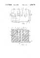
- FIG. 1is a top view of a multilayer circuit board showing a through-hole, three blind-holes, and top and embedded metallic via patterns;
- FIG. 2is a cross-sectional view, across II--II of FIG. 1, showing the through-hole and the three blind-holes;
- FIG. 3is a sectional view of a portion of FIG. 2, showing a metal-plated blind-hole, and the connection between a top and imbedded metal via;
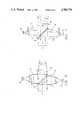
- FIG. 4is a schematic diagram of one embodiment of the laser drilling system of this invention.
- FIG. 5, which best illustrates the invention,is a schematic diagram of one embodiment of the laser focusing head which contains the combined reflected beam optical and reflected optical, radiation detection systems of this invention, which can be utilized to control laser drilling depth;
- FIG. 6is a schematic diagram of a first modified optical system useful in this invention to reduce the area required of the reflected radiation detectors.
- FIG. 7is a schematic diagram of a second modified optical system useful in this invention to allow beam splitting mirrors in the reflected beam optical system of this invention.
- Holes 15, 17, and 18are "blind-holes,” i.e., holes that pass through the body of the laminate, and end at either an embedded wire, via, or the bottom metal cladding sheet.
- Hole 16is a "through-hole,” i.e., a hole that passes through the entire laminate.
- the laminate 26, shown in FIG. 2can be made from plural layers of resin impregnated fibrous sheet material.
- the fibrous sheetcan be woven or unwoven glass fibers, high purity fibrous quartz, aromatic polyamide fibers (such as Kevlar), polyethylene terephthalate fibers (such as Dacron), cellulosic paper fibers (such as Kraft paper), and the like.
- a laminatemay also contain mixtures of fibrous sheet material, for example a top layer of impregnated glass cloth and a base of impregnated cellulosic fibers, such as Kraft paper.
- the laminatemay comprise two to eight or more sheets, with a total laminate thickness of from about 4 mil to 250 mil (0.1 mm to 6.3 mm), usually about 20 mil to 120 mil (0.5 mm to 3 mm).
- Useful resins for impregnating the laminate sheetscan include phenolic resins, polyester resins, polyimide resins, polytetrafluoroethylene (such as Teflon), and the like resins, or most preferably epoxy resins, all of which are well known in the art. In many instances a flame retardant epoxy resin is most preferred.
- Useful flame retardant epoxy resinscan include brominated epoxy resin; or a mixture of non-halogenated epoxy resin such as bisphenol A epoxy, cycloaliphatic epoxy, novolac epoxy or their mixtures, with a flame retarding reactive additive containing, for example, bromine and phenolic hydroxyl groups, preferably tetrabromobisphenol A.
- a phenolic novolaccan be used as the curing agent, among others, and optional catalysts could include tertiary amines, imidazoles, and the like.
- Additional flame retardant additives, to impart an additional degree of flame resistance,can include antimony trioxide, antimony pentoxide, and various phosphates.
- FIG. 3shows a detailed view of a metal-plated blind hole 18, laser-drilled by the invention apparatus.
- Plating 30is with copper and the like metal, usually by a combination of electrodeless and electroplating techniques, to provide electrical leads through the circuit board to connect various imbedded wires or vias.
- electrical componentssuch as diodes, transistors and the like are soldered to a top conductor pad, for example at position 31.
- drilling holes by the method of this inventionprovides a clean bottom contact at metal via 23, with a minimal cavity or void on the sides of the via which would create plating problems.
- FIG. 4shows, in general, one embodiment of the preferred, dual laser drilling system of this invention, which may be used, for example, to precisely laser drill blind holes and through holes in a wide variety of workpieces, such as those shown in the multilayer circuit board laminate of FIGS. 1 to 3. Each laser can be used separately or both can be used at the same time.
- Workpiece 10is shown on positioning table 40 at a drilling station.
- the positioning tablecould be X-Y direction programmed to move through a preset sequence via a computer program.
- the drillingwould take place in an environmental chamber to control the debris and vapors from the laser drilling and to prevent workpiece contamination.
- Two laser transmitting means 41 and 42are shown, containing any required laser heads, power sources, cavity mirrors, aperture stop elements, Q switches, collimation optics, and the like, providing original laser beams 56 and 57, one of which is shown reflected at mirror 51.
- the laser transmitting means 41can, however, be initially positioned so that its original laser beam 56 is 90° to original laser beam 57. In some operations only a single laser transmitting means need be used with the depth-monitoring, optical-radiation detecting means of this invention, for example, when only shallow blind holes are to be laser-drilled in a workpiece.
- the original laser beamhas associated with it a first optical system, which can include optical elements 67, 68, 58 and 61, shown in FIG. 5, for focusing the original laser beam on the workpiece and either passing or reflecting the original laser beam to the workpiece.
- This first optical systemis also used for passing or reflecting the laser beam reflected from the workpiece to a second optical system, which can include optical elements 63 and 64, shown in FIG. 5.
- the second optical systemcomprises means capable of reflecting a selected portion of the original laser beam into one part of detector means 45 or 46.
- the second optical systemis also capable of reflecting a portion of the laser beam reflected from the workpiece into a second part of detector means 45 or 46.
- a long wavelength, laser transmitting means 41is used to emit an original laser beam 56 having a power density capable of penetrating and vaporizing non-metallic material, such as organic resin impregnated fibrous material.
- Original laser beam 56is reflected by mirror 51 to direct it to the workpiece 10.
- This long wavelength laser beamis substantially completely reflective from metal (about 90% or more) and is defined as having a wavelength of preferably from about 8 microns to about 15 microns.
- Such a lasercould be a pulsed CO 2 laser type, which is well known in the art. This laser would provide an original laser beam having a wavelength, preferably of from about 9 microns to about 11 microns, usually 10.6 microns.
- a short wavelength laser transmitting means 42is used to emit an original laser beam 57, having a power density capable of penetrating and vaporizing non-metallic material, such as organic resin impregnated fibrous material, and also metal.
- This short wavelength laser beamhas substantial reflection from metal (about 30% to about 60%) and is defined as having a wavelength of preferably from about 0.4 micron to about 3 microns.
- Such a lasercould, preferably, be a pulsed Neodymium--YAG (neodymium doped yttrium aluminum garnet) or Neodymium-glass laser, which are both well known in the art. These lasers would provide an original laser beam having a short wavelength, preferably of from about 1 micron to about 2 microns, usually 1.06 microns.
- the short wavelength laserWhen used, it should be operated in a pulsed mode, to control the drilling, and prevent excessive damage to both the metal cladding or vias and the insulating substrate. In most instances, only infrared radiation (over 0.78 micron wavelength) will be used to laser drill the workpiece.
- Drilling depth monitoring meansshown enclosed by dashed line 43 in FIG. 4, comprises a laser-focusing head and a plurality of optical means, described in detail in FIG. 5.
- This drilling depth monitoring meansis capable of transmitting the reflected laser beam radiation from the workpiece 10, when the focused laser beam(s) 44 contacts various components of the workpiece 10.
- the monitoringalso contains at least two optical, radiation detectors 45 and 46, which are capable of receiving radiation and quickly converting it to electrical signals, and the whole can be utilized to control laser drilling depth.
- laser beam(s) 44is usually substantially vertical (about 90° ⁇ 5°) to the workpiece.
- a television camera 47 connected to a television monitor 48can be used to observe the laser drilling at the workpiece.
- Positioning controls 49connected to the positioning table 40, control alignce of the workpiece 10, so that holes are laser-drilled at desired locations on the workpiece. After laser drilling, the workpiece is moved to a plating means station 50 to plate the surfaces of the laser-drilled holes and other portions of the workpiece as desired.
- a focused laser beamdrills a hole by heating a small volume of material to a sufficiently high temperature for localized melting and/or vaporization to occur.
- the characteristics of the drilled holewill depend on a number of factors, including the laser beam power and pulse parameters, the laser wavelength, and the heat transfer properties of the material.
- One feature of laser drilling, which is utilized in this invention,is that a long wavelength laser beam, such as produced by a CO 2 laser, is readily absorbed by a dielectric material, while reflected by a metallic surface. Provided that the incident laser power onto the metallic surface is not too high, the metal is not damaged, and near total reflection of the laser beam occurs.
- a shorter wavelength laser beamsuch as produced by a Neodymium--YAG laser, will be more readily absorbed by a metal surface, thereby producing a drilled hole through the metal.
- a short wavelength laser 42such as a Neodymium--YAG laser
- the laser beamwould usually be focused to converge somewhere between metal vias 21 and 24 in the workpiece, or the beam could be continuously refocused as it proceeded through the substrate.
- the short wavelength laser beamwould first vaporize copper wire 13, to provide a hole 16 of, for example, 2 mil (0.05 mm) diameter. A clean hole with a flat surface will result if there is good integrity between the copper and the substrate.
- the laser beamwould then vaporize epoxy resin and glass cloth down to copper via 21 where it would contact and penetrate copper, and so on through bottom copper sheet 25 as shown in FIG. 2.
- the bottom hole through sheet 25would have a diameter of about 1.5 mil (0.038 mm); i.e., it would be slightly smaller than the top hole at entry and the length of the hole through the workpiece would be slightly tapered. This would provide a ratio of entry diameter/exit diameter of 1/1.5.
- both a short wavelength laser 42, such as a Nd--YAG laser, and a long wavelength laser 41, such as a CO 2 laser,would preferably be used.
- the short wavelength laser beamwould first vaporize the top copper via to provide hole 18 or 15 of, for example, 2 mil diameter. A substantial amount of reflected radiation would be monitored by detector 46', which radiation monitored would drop upon entry into the laminate substrate material 26.
- the short wavelength lasercould be quickly turned off, or it could be allowed to penetrate close to via 23 or wire 20.
- the long wavelength laser beamwould be used to vaporize the laminate substrate material 26, where contact with the epoxy-glass would reflect minor radiation (about 5% to about 25%), down to the surface of via 23 or wire 20.
- This minor amount of reflected radiationwould be monitored by detector 45', which radiation monitored would dramatically increase upon laser beam contact with metal, due to substantially complete reflection of the laser beam (over about 95%).
- the long wavelength laserUpon reaching the depth of the surface of metal via 23 or wire 20, the long wavelength laser would be quickly turned off.
- the turn on shut off switchcould be controlled by a programmed computer or the like, receiving electrical signals directly from the detectors, thus operating as a measuring means, or from a measuring means connected to the detectors, so that laser on off reaction kime would be substantially instantaneous.
- the depth of laser drillingcould be measured by optical means, feeding reflected radiation into suitable, optical radiation detectors.
- the CO 2 lasercould be used between vias.
- short wavelength laser drillingis preferred, since it produces cleaner holes, having better definition and smoother sides that are easier to plate than if laser drilling is by a long wavelength laser.
- a suitable registering meanscould initially be used, prior to any laser drilling operations, to ensure proper alignment of all the layered metallic vias or wires, so that the drilled holes do not miss imbedded vias or wires. Such registering techniques are well known in the art.
- This monitoring meanscontains the reflected beam optical system and the optical, radiation detection system of this invention, which, in combination, can be utilized to quickly control laser drilling depth and to prevent overrun or harm to imbedded metallic conductors.
- This monitoring meansallows simultaneous or consecutive focusing of long wavelength laser beam 56, such as a CO 2 laser beam, and short wavelength laser beam 57, suc as a Neodymium--YAG laser beam, onto a point on the workpiece 10 placed on movable positioning table 40.
- the laser beamwill enter the workpiece in a substantially transverse (about 90° ⁇ 5°) direction.
- Components 45', 45", 46' and 46"are radiation detectors that receive and quickly measure the incident, original and reflected laser radiation.
- Component 47is a television camera that provides a means for viewing the laser drilling operation via an associated television monitor.
- Optical element 58positioned above the point to be drilled in the workpiece 10 and the focal point of the laser beam 59, serves three distinct functions. Its bottom or lower surface 60 has a suitable dichroic coating so that it will reflect the original short wavelength laser beam 57 incident from the left. Application techniques for such dichroic coatings are well known in the art.
- the body of optical element 58is made from a material, such as single or polycrystalline alkali salt, for example NaCl, KCl and the like, that will transmit, i.e., pass, both visible light (radiation) and the original long wavelength laser beam 56.
- the optical element 61disposed above the short wavelength laser beam reflective mirror 58, can also be made of a material such as single or polycrystalline alkali salt as described above, that will transmit both visible light (radiation) and the long wavelength laser beam 56, however its lower surface has a suitable dichroic coating so that it will have a high reflectivity to visible light, yet transmit, i.e., pass, long wavelength laser beams.
- Mirror 61transmits, i.e., passes, the original long wavelength laser beam 56 that is incident from above, and, by reflecting light from the workpiece into television camera 47, also provides a means for viewing the laser drilling operation via an associated television monitor.
- the required functions of optical elements 58 and 61can be satisfied by present, well-known, conventional, state of the art, dichroic coating technology.
- the optical element 61 and television camera 47are preferred, but other means may be utilized to view the drilling.
- original laser beam 57reflects off of optical element surface 60, and, incident from above at about a 90° angle, focuses onto workpiece 10, such as the printed circuit board of FIGS. 1 and 2, where it usually contacts metal vias.
- workpiece 10such as the printed circuit board of FIGS. 1 and 2, where it usually contacts metal vias.
- the laser beamvaporizes a hole through the metal, a substantial amount of the radiation 57' being reflected back, where it is finally reflected by appropriate means 63 into a radiation detector 46'.
- Laser beam 56can be utilized, where it passes through optical elements 61 and 58, and focuses onto workpiece 10.
- That laser beammay contact laminate substrate material, for example, epoxy resin impregnated glass fiber cloth and vaporize a hole therethrough until it contact a metal via or wire, whereupon substantially all of the long wavelength laser beam radiation 56' is reflected back through optical elements 58 and 61, and is finally reflected by appropriate means 64 into a radiation detector 45', which outputs electrical signals similarly to detector 46'.
- the long wavelength laser beam 56contacts glass-epoxy, the reflected radiation passed to detector 45' will result in a "low” signal output, but, when laser beam 56 contacts metal, where there is almost total reflection, the detector 45' will output a "high” signal. This sudden burst of signal can be monitored by a variety of measuring means, and utilized to quickly shut off the laser.
- Visible light beams 65reflect from the workpiece 10, pass through optical element 58, and are primarily reflected off of optical element surface 62, into television camera 47.
- Both sets of signal detectors 45', 46' and 45" and 46"which can be of well known pyroelectric, photovoltaic or heat sensitive types, are capable of quickly converting the reflected radiation they receive into an electrical signal, and are connected to means 66, such as a voltmeter, computer, or the like, to quickly measure variations in the electrical signals.
- the variations in electrical signalscan be fed to a stop-start means, such as a programmed computer, which can substantially instantaneously stop or start both laser transmitting means.
- Optical element lenses 67 and 68are effective to focus the laser beams, and are located at a position such that the laser beams come to focus at a desired position on or within the workpiece. These are movable along their axis by an appropriate means, so that the focal point can be moved if desired as a hole is laser-drilled into and through the workpiece.
- Partially laser beam reflecting, partially laser beam transmitting optical members 63 and 64are shown in FIG. 5. They can have holes through their centers, with the outer portions remaining to reflect radiation, so that an outer portion of each original laser beam, i.e., 56" and 57", is "skimmed"
- optical members 63 and 64have either a cutout center portion, or a center portion that transmits, i.e., passes, original laser beam radiation 57 and 56, respectively.
- the edge portions of optical members 63 and 64are effective to reflect laser beam radiation 57' and 56' respectively to optical radiation detectors.
- the open window or transparent portionsare shown as lengths 69 in FIG. 5.
- the difference in signal over time sent out by optical signal detectors 45' and 46'is compared and measured by measuring means 66.
- the return radiation signal levels sent out or transmitted by detectors 45' and 46', from reflected laser radiation 56' and 57'will vary depending on the material the laser beam is contacting, and measuring means 66, such as a voltmeter, computer, or the like can indicate the level of difference, and pass it to a computerized laser on-off switch.
- This measurementcan be used to differentiate when a laser contacts or passes into metal or substrate material. Even as laser drilling gets deeper and possibly some reflected radiation is absorbed exiting the workpiece, there will still be dramatic signal differences between metal and laminate material contact which are measurable by means 66 to allow start or shut down of the laser beam(s).
- Measuring means 66need not be connected to detectors 45" and 46", any circuitry being used which is effective to measure difference in output signals over time from detectors 45' and 46', which receive reflected radiation from the workpiece.
- FIG. 6an alternative embodiment of the optics associated with the radiation detectors and original laser beam is shown.
- the short wavelength laser beam 57a change has been made to incorporate additional optical element lenses 70, disposed between partially transmitting, partially reflecting optical element 63 and detectors 46' and 46", to narrow, or focus to a small area, the radiation reflected from optical element 63 onto detectors 46' and 46".
- This embodimentallows se of smaller area detectors.
- a similar change to the long wavlength radiation detectorsis also part of this embodiment.
- FIG. 7another alternative embodiment of the optics associated with this invention is shown, again using the short wavelength laser beam 57 as an example.
- Partially reflecting, partially transmitting optical element 63 in FIGS. 5 and 6is substituted for by an optical element semi-reflective of incident radiation 57.
- Mirror 75reflects a known fraction of original laser beam radiation 57 and reflected radiation 57', for example, about 5% to about 20%, allowing from about 80% to about 95% of radiation transmittal.
- Thisserves the same purpose as center cut out optical element 63 in prior embodiments, and may be easier to fabricate, install, and adjust. It can also be used with the additional optical element lenses 70 shown in FIG. 7.
- a similar change to the long wavelength radiation detectorsis also part of this embodiment.
- the laminatewas made of epoxy resin impregnated glass cloth, with 1/3 ounce (0.0004 inch thick) copper cladding on both faces.
- a 7 ⁇ 8 array of 2 mil (0.002”) diameter holeswere drilled through the entire PWB using the laser operated at a power level of about 3 Watts, and at a pulse repetition rate of 4000 Hz. Two 100 millisecond bursts of laser pulses were required to drill the holes.
- the diameters of the exit holes on the backside of the PWBaveraged 1.5 mil.
- a Photon Sources Model V500, CO 2 laser, having a wavelength of 10.6 microns, and a maximum power of about 475 wattswas used to successively drill "blind"-holes in a laminate.
- the CO 2 laser beamwas routed via a series of mirrors to a 5-inch focal length lens, which focused the laser beam at a sample laminate comprising a top, organic resin impregnated fabric material, clad on the bottom side with 1 ounce (0.0012 inch thick) copper.
- a series of "blind"-holeswere laser-drilled, as described in Table 1 below:
- optimum blind-hole drillingoccurs in all but the epoxy-Kevlar laminates at about 50 Watts, and from about 0.2 Joules to 0.8 Joules total energy.
- Each resin-substrate systemwould have to be tailored in this regard.
- Laser energies of about 0.8 Joulesare appropriate for Teflon-Kevlar; about 0.1 Joules may be appropriate for epoxy-Kevlar; and about 0.2 Joules appear to be appropriate for polyimide-glass and epoxy-glass, especially if thicker laminate bodies were used.
Landscapes
- Physics & Mathematics (AREA)
- Optics & Photonics (AREA)
- Engineering & Computer Science (AREA)
- Plasma & Fusion (AREA)
- Mechanical Engineering (AREA)
- Manufacturing & Machinery (AREA)
- Microelectronics & Electronic Packaging (AREA)
- Laser Beam Processing (AREA)
Abstract
Description
TABLE 1 __________________________________________________________________________CO2 LASER BLIND-HOLE DRILLING IN BOTTOM COPPER CLAD CIRCUIT BOARD SAMPLES Sample Condition at Laser Focus For Resin-Substrate (Thickness) Energy Pulse Teflon-Kevlar Epoxy-Kevlar Polyimide-Glass Epoxy-Glass Total Per Duration (0.028") (0.024") (0.010") (0.006") Power Energy Pulse No. On Off Dia. Dia. Dia. Dia. Watts J J/Pulse # ms ms Observation mil Observation mil Observation mil Observation mil __________________________________________________________________________100 2 2 1 20 -- B,H 12 P 19 P,B 19 B,H 20 100 2 0.2 10 2 2 P 14 P 15 P 20 B,H 20 50 1 1 1 20 -- B 12 B,P 14 B,H 16 B,H 16 50 1 0.25 4 5 10 B,P 12 B,P 13 B,H 16 B,H 16 50 1 0.25 4 5 500 B,P 10 -- -- -- -- -- -- 50 0.8 0.1 8 2 500 B 10 -- -- -- -- -- -- 50 0.8 0.05 16 1 500 B 9 -- -- -- -- -- -- 50 0.4 0.1 4 2 500 B 10 -- -- -- -- -- -- 50 0.2 0.1 2 2 50 N 9 B,P 10 B* 12 B,H 11 50 0.4 0.1 4 2 50 B 10 B,P 10 B,P 14 B,H 13 50 0.8 0.1 8 2 50 B* 10 B,P 11 B 16 B,H 16 50 0.2 0.05 4 1 50 N 10 B 10 B 11 B*,H 13 50 0.4 0.05 8 1 50 B 10 B,P 10 B 12 B,H 14 50 0.8 0.05 16 1 50 B* 10 B,P 11 B 14 B,H 16 50 0.2 0.1 2 2 500 N 10 B* 10 B* 12 B,H 12 50 0.4 0.1 4 2 500 B 10 B,P 10 B 14 B,H 14 50 0.8 0.1 8 2 500 B* 10 B,P 11 B 14 B,H 16 50 0.2 0.05 4 1 500 N 9 B,P 10 B* 12 B,H 12 50 0.4 0.05 8 1 500 B 10 B,P 10 B 13 B,H 14 50 0.8 0.05 16 1 500 B* 10 B,P 11 B 15 B,H 15 __________________________________________________________________________ Letter Code: N= Hole not through to copper ms = Microseconds Teflon = Polytetrafluoroethylene Kevlar = Aromatic polyamide fibers * = Best blindhole to copper surface B = Blindhole to copper surface P = Puncture copper with 2-4 mil diameter hole H = Heating of copper evident by rings/discoloration J = Joules
Claims (18)
Priority Applications (5)
| Application Number | Priority Date | Filing Date | Title |
|---|---|---|---|
| US07/073,610US4789770A (en) | 1987-07-15 | 1987-07-15 | Controlled depth laser drilling system |
| CA000570861ACA1306019C (en) | 1987-07-15 | 1988-06-30 | Controlled depth laser drilling system |
| EP88306319AEP0299702A1 (en) | 1987-07-15 | 1988-07-11 | Controlled depth laser drilling system |
| JP63176878AJP2686470B2 (en) | 1987-07-15 | 1988-07-15 | Depth control laser drilling method and apparatus |
| KR1019880008841AKR0121792B1 (en) | 1987-07-15 | 1988-07-15 | Controlled depth laser drilling device and method |
Applications Claiming Priority (1)
| Application Number | Priority Date | Filing Date | Title |
|---|---|---|---|
| US07/073,610US4789770A (en) | 1987-07-15 | 1987-07-15 | Controlled depth laser drilling system |
Publications (1)
| Publication Number | Publication Date |
|---|---|
| US4789770Atrue US4789770A (en) | 1988-12-06 |
Family
ID=22114730
Family Applications (1)
| Application Number | Title | Priority Date | Filing Date |
|---|---|---|---|
| US07/073,610Expired - LifetimeUS4789770A (en) | 1987-07-15 | 1987-07-15 | Controlled depth laser drilling system |
Country Status (5)
| Country | Link |
|---|---|
| US (1) | US4789770A (en) |
| EP (1) | EP0299702A1 (en) |
| JP (1) | JP2686470B2 (en) |
| KR (1) | KR0121792B1 (en) |
| CA (1) | CA1306019C (en) |
Cited By (95)
| Publication number | Priority date | Publication date | Assignee | Title |
|---|---|---|---|---|
| US4870244A (en)* | 1988-10-07 | 1989-09-26 | Copley John A | Method and device for stand-off laser drilling and cutting |
| US4995087A (en)* | 1989-05-15 | 1991-02-19 | General Electric Company | Machine vision system |
| US4998005A (en)* | 1989-05-15 | 1991-03-05 | General Electric Company | Machine vision system |
| US5013886A (en)* | 1990-07-23 | 1991-05-07 | General Electric Company | Real-time magnetic-flux breakthrough detection method and system for laser drilling |
| US5022960A (en)* | 1989-05-01 | 1991-06-11 | Ibiden Co., Ltd. | Method of manufacturing circuit board for mounting electronic components |
| US5059761A (en)* | 1990-12-21 | 1991-10-22 | General Electric Company | Inductive depth sensing and controlling method and system for laser drilling |
| US5126532A (en)* | 1989-01-10 | 1992-06-30 | Canon Kabushiki Kaisha | Apparatus and method of boring using laser |
| US5126530A (en)* | 1989-11-29 | 1992-06-30 | Mercedes-Benz Ag | Method for producing hollow gas exchange valves for reciprocating engines |
| US5166493A (en)* | 1989-01-10 | 1992-11-24 | Canon Kabushiki Kaisha | Apparatus and method of boring using laser |
| US5168454A (en)* | 1989-10-30 | 1992-12-01 | International Business Machines Corporation | Formation of high quality patterns for substrates and apparatus therefor |
| US5227606A (en)* | 1992-02-26 | 1993-07-13 | U.S. Amada Ltd. | Method and apparatus for laser cutting of multiple stacked metal worksheets |
| US5246576A (en)* | 1990-12-10 | 1993-09-21 | Ppg Industries, Inc. | Cathode in a layered circuit and electrochemical cell for a measurement of oxygen in fluids |
| US5283417A (en)* | 1989-12-07 | 1994-02-01 | Research Development Corporation Of Japan | Laser microprocessing and the device therefor |
| US5367143A (en)* | 1992-12-30 | 1994-11-22 | International Business Machines Corporation | Apparatus and method for multi-beam drilling |
| US5372666A (en)* | 1989-10-25 | 1994-12-13 | E. I. Du Pont De Nemours And Company | Method of manufacturing a multilayered circuit board |
| EP0642846A1 (en)* | 1993-08-12 | 1995-03-15 | ONET Société Anonyme | Method and device for self-controlling laser decontamination of surfaces |
| WO1995009713A1 (en)* | 1993-10-01 | 1995-04-13 | Universität Stuttgart Institut für Strahlwerkzeuge | Process and device for determining the momentary and maintaining the desired depth of penetration of a machining laser beam into a workpiece |
| US5530204A (en)* | 1990-11-27 | 1996-06-25 | Ibiden Co., Ltd. | Electronic-parts mounting board and electronic-parts mounting board frame |
| US5541731A (en)* | 1995-04-28 | 1996-07-30 | International Business Machines Corporation | Interferometric measurement and alignment technique for laser scanners |
| US5562842A (en)* | 1994-10-17 | 1996-10-08 | Panasonic Technologies, Inc. | Material treatment apparatus combining a laser diode and an illumination light with a video imaging system |
| US5609778A (en)* | 1995-06-02 | 1997-03-11 | International Business Machines Corporation | Process for high contrast marking on surfaces using lasers |
| US5618454A (en)* | 1995-04-28 | 1997-04-08 | International Business Machines Corporation | Multi-wavelength programmable laser processing mechanisms and apparatus utilizing design data translation system |
| US5670068A (en)* | 1994-04-26 | 1997-09-23 | Matsushita Electric Industrial Co., Ltd. | Apparatus for laser processing and monitoring |
| EP0827802A1 (en)* | 1996-09-07 | 1998-03-11 | JENOPTIK Aktiengesellschaft | Method to produce a weakening line using a laser |
| US5751588A (en)* | 1995-04-28 | 1998-05-12 | International Business Machines Corporation | Multi-wavelength programmable laser processing mechanisms and apparatus utilizing vaporization detection |
| US5808268A (en)* | 1996-07-23 | 1998-09-15 | International Business Machines Corporation | Method for marking substrates |
| US5806155A (en)* | 1995-06-07 | 1998-09-15 | International Paper Company | Apparatus and method for hydraulic finishing of continuous filament fabrics |
| US5826330A (en)* | 1995-12-28 | 1998-10-27 | Hitachi Aic Inc. | Method of manufacturing multilayer printed wiring board |
| DE19719700A1 (en)* | 1997-05-09 | 1998-11-12 | Siemens Ag | Blind hole production in circuit board |
| US5841099A (en)* | 1994-07-18 | 1998-11-24 | Electro Scientific Industries, Inc. | Method employing UV laser pulses of varied energy density to form depthwise self-limiting blind vias in multilayered targets |
| US5841102A (en)* | 1996-11-08 | 1998-11-24 | W. L. Gore & Associates, Inc. | Multiple pulse space processing to enhance via entrance formation at 355 nm |
| US5870807A (en)* | 1995-11-17 | 1999-02-16 | Bba Nonwovens Simpsonville, Inc. | Uniformity and product improvement in lyocell garments with hydraulic fluid treatment |
| US5939704A (en)* | 1994-04-05 | 1999-08-17 | British Nuclear Fuels Plc | Radiation beam position sensor |
| GB2337719A (en)* | 1998-05-27 | 1999-12-01 | Exitech Ltd | Method and apparatus for drilling microvia holes in electrical circuit interconnection packages |
| US6054673A (en)* | 1997-09-17 | 2000-04-25 | General Electric Company | Method and apparatus for laser drilling |
| WO2001019146A1 (en)* | 1999-09-06 | 2001-03-15 | Siemens Aktiengesellschaft | Method for treating multiple-layer substrates |
| US6211485B1 (en)* | 1996-06-05 | 2001-04-03 | Larry W. Burgess | Blind via laser drilling system |
| DE10048636A1 (en)* | 2000-09-27 | 2002-04-18 | Jenoptik Jena Gmbh | Airbag cover with predetermined breaking line and process for its production |
| US6430465B2 (en) | 2000-01-11 | 2002-08-06 | Electro Scientific Industries, Inc. | Abbe error correction system and method |
| US6433301B1 (en)* | 1999-05-28 | 2002-08-13 | Electro Scientific Industries, Inc. | Beam shaping and projection imaging with solid state UV Gaussian beam to form vias |
| US6437283B1 (en)* | 1999-11-29 | 2002-08-20 | Siemens Aktiengesellschaft | Device and method for processing substrates |
| US6462306B1 (en) | 1999-04-27 | 2002-10-08 | Gsi Lumonics, Inc. | System and method for material processing using multiple laser beams |
| US20020185474A1 (en)* | 2001-05-09 | 2002-12-12 | Dunsky Corey M. | Micromachining with high-energy, intra-cavity Q-switched CO2 laser pulses |
| US20020190038A1 (en)* | 2001-03-16 | 2002-12-19 | Laser Machining, Inc. | Laser ablation technique |
| US20030006220A1 (en)* | 2001-07-02 | 2003-01-09 | Michael Cummings | Method of ablating an opening in a hard, non-metallic substrate |
| US6541731B2 (en)* | 2000-01-25 | 2003-04-01 | Aculight Corporation | Use of multiple laser sources for rapid, flexible machining and production of vias in multi-layered substrates |
| US6580055B2 (en)* | 2000-06-09 | 2003-06-17 | Sumitomo Heavy Industries, Ltd. | Laser processing apparatus and method |
| US6624382B2 (en)* | 1997-01-30 | 2003-09-23 | Anvik Corporation | Configured-hole high-speed drilling system for micro-via pattern formation, and resulting structure |
| US6631558B2 (en)* | 1996-06-05 | 2003-10-14 | Laservia Corporation | Blind via laser drilling system |
| US20030213787A1 (en)* | 1999-05-28 | 2003-11-20 | Dunsky Corey M. | Beam shaping and projection imaging with solid state UV gaussian beam to form vias |
| US6720567B2 (en) | 2001-01-30 | 2004-04-13 | Gsi Lumonics Corporation | Apparatus and method for focal point control for laser machining |
| US20040094525A1 (en)* | 2002-08-01 | 2004-05-20 | Jurgen-Michael Weick | Laser processing machine |
| US20040173942A1 (en)* | 2001-05-11 | 2004-09-09 | Nobutaka Kobayashi | Method and device for laser beam machining of laminated material |
| US6791057B1 (en)* | 1998-11-12 | 2004-09-14 | Fraunhofer-Gesellschaft Zur Forderung Der Angewandten Forschung E.V. | Method and device for machining workpieces using high-energy radiation |
| US20050128672A1 (en)* | 2003-09-19 | 2005-06-16 | Tourne Joseph A. | Closed loop backdrilling system |
| US20050157172A1 (en)* | 2004-01-21 | 2005-07-21 | Richard Hartley | Video signal processor |
| US20050169717A1 (en)* | 2004-02-03 | 2005-08-04 | Field Grant A. | Electronic drill depth indicator |
| US20050184035A1 (en)* | 1995-08-07 | 2005-08-25 | Mitsubishi Denki Kabushiki Kaisha | Pulsed laser beam machining method and apparatus for machining a wiring board at multiple locations |
| EP1073321A3 (en)* | 1999-07-27 | 2005-09-07 | Matsushita Electric Works, Ltd. | Processing method of printed wiring board |
| US20060068581A1 (en)* | 2003-10-06 | 2006-03-30 | Shinko Electric Industries Co., Ltd. | Method of forming via hole in resin layer |
| US20060090933A1 (en)* | 2004-10-29 | 2006-05-04 | Timothy Wig | Apparatus and method for improving printed circuit board signal layer transitions |
| US20060096964A1 (en)* | 2004-11-08 | 2006-05-11 | Fordahl Craig A | Method and apparatus for breakthrough detection for laser workpiece processing operations |
| US20060124615A1 (en)* | 2003-05-22 | 2006-06-15 | Masayuki Azuma | Laser dicing device |
| US7062845B2 (en) | 1996-06-05 | 2006-06-20 | Laservia Corporation | Conveyorized blind microvia laser drilling system |
| US20070189347A1 (en)* | 2003-03-18 | 2007-08-16 | Denney Paul E | Method and apparatus for material processing |
| US20070207233A1 (en)* | 1994-10-31 | 2007-09-06 | Bauer David J | Apparatus for producing a preweakened automotive interior trim piece for covering an air bag installation in an automovtive vehicle |
| US20070289957A1 (en)* | 2003-11-10 | 2007-12-20 | Sauer Gmbh | Laser Machining Apparatus and Laser Machining Method |
| US20080067331A1 (en)* | 2003-03-18 | 2008-03-20 | Denney Paul E | Method and apparatus for detecting embedded material within an interaction region of a structure |
| US20080264910A1 (en)* | 2004-09-14 | 2008-10-30 | Raman Kashyap | Process for Fabricating Optical Waveguides |
| US20090283506A1 (en)* | 2008-05-15 | 2009-11-19 | Mitutoyo Corporation | Laser processing apparatus |
| US20090321395A1 (en)* | 2007-08-15 | 2009-12-31 | Caterpillar Inc. | Variable focus laser machining system |
| EP1832376A3 (en)* | 2006-03-06 | 2010-04-28 | General Electric Company | System and method for monotoring drilling process parameters and controlling drilling operation |
| CN102489876A (en)* | 2011-11-11 | 2012-06-13 | 北京中科思远光电科技有限公司 | Laser annealing method and laser annealing device adopting laser auxiliary heating |
| DE10149559B4 (en)* | 2000-10-06 | 2012-12-20 | Hitachi Via Mechanics, Ltd. | Apparatus and method for laser processing a printed wiring board |
| US20130068736A1 (en)* | 2011-09-21 | 2013-03-21 | Michael Mielke | Systems and processes that singulate materials |
| US20130288425A1 (en)* | 2011-08-05 | 2013-10-31 | Solexel, Inc. | End point detection for back contact solar cell laser via drilling |
| US20130333214A1 (en)* | 2011-03-01 | 2013-12-19 | Snecma | Process for manufacturing a metal part, such as turbine engine blade reinforcement |
| US8624158B2 (en) | 2003-03-18 | 2014-01-07 | Loma Linda University Medical Center | Manipulation apparatus for system that removes material from a surface of a structure |
| US8630731B2 (en)* | 2006-11-30 | 2014-01-14 | National Optronics, Inc. | Method of calibrating an ophthalmic processing device, machine programmed therefor, and computer program |
| US20140053399A1 (en)* | 2012-08-27 | 2014-02-27 | Micronic Mydata AB | Maskless writing of a workpiece using a plurality of exposures having different focal planes using multiple dmds |
| US8663770B2 (en) | 2011-04-28 | 2014-03-04 | Zin Technologies, Inc. | Bonded and stitched composite structure |
| WO2014064017A3 (en)* | 2012-10-22 | 2014-08-07 | Trumpf Werkzeugmaschinen Gmbh + Co. Kg | Method and processing machine for grooving, drilling or cutting metal workpieces, with determination of the intensity of the process radiation |
| EP3042732A1 (en)* | 2015-01-08 | 2016-07-13 | General Electric Company | Method of and system for confined laser drilling of a hole in a near wall of a component |
| US9458728B2 (en) | 2013-09-04 | 2016-10-04 | Siemens Energy, Inc. | Method for forming three-dimensional anchoring structures on a surface by propagating energy through a multi-core fiber |
| CN104781036B (en)* | 2012-10-22 | 2016-11-30 | 通快机床两合公司 | Method and processing machine for drilling and cutting metal workpieces by determining the radiation intensity of the process |
| US20170057018A1 (en)* | 2015-08-28 | 2017-03-02 | Chun-hao Li | Double-directional machining laser machine tool |
| CN107470786A (en)* | 2017-09-14 | 2017-12-15 | 深圳市牧激科技有限公司 | More laser head assemblies |
| US10932370B2 (en) | 2018-06-28 | 2021-02-23 | Drilliant Ltd | Metal sublayer sensing in multi-layer workpiece hole drilling |
| US10933490B2 (en) | 2015-12-22 | 2021-03-02 | Drilliant Ltd. | Metal sublayer sensing in multi-layer workpiece hole drilling |
| US20210360793A1 (en)* | 2020-05-14 | 2021-11-18 | Skybrain Vermögensverwaltungs Gmbh | Machining Station and Method for Machining Workpieces |
| CN114222429A (en)* | 2021-11-30 | 2022-03-22 | 深圳博悦智能有限公司 | Deep drilling method for circuit board, depth setting drill bit and circuit board Finalv2 |
| CN114245579A (en)* | 2021-12-11 | 2022-03-25 | 深圳博悦智能有限公司 | A circuit board fixed-depth hole processing device |
| CN114745871A (en)* | 2022-03-21 | 2022-07-12 | 江西福昌发电路科技有限公司 | A laser drilling ash removal process for HDI circuit board production |
| US11440140B2 (en)* | 2017-04-12 | 2022-09-13 | Eissmann Automotive Deutschland Gmbh | Method for introducing a defined weakening line by means of a pulsed laser beam via material removal on a cover material |
| US11690177B2 (en) | 2020-04-07 | 2023-06-27 | Nextgin Technology Bv | Methods and systems for back-drilling a multi-layer circuit board |
Families Citing this family (16)
| Publication number | Priority date | Publication date | Assignee | Title |
|---|---|---|---|---|
| JP2717179B2 (en)* | 1988-09-21 | 1998-02-18 | 株式会社ソディック | Laser forming equipment |
| DE68919328T2 (en)* | 1988-10-28 | 1995-05-24 | Ibm | Ultraviolet laser ablation and etching of organic solids. |
| DE3908187A1 (en)* | 1989-03-14 | 1990-09-20 | Jurca Marius Christian | METHOD FOR QUALITY ASSURANCE IN LASER BEAM WELDING AND CUTTING |
| AT399117B (en)* | 1991-05-27 | 1995-03-27 | Schuoecker Dieter Dipl Ing Dr | Method for the automated quality control of laser machining |
| GB9122010D0 (en)* | 1991-10-15 | 1991-12-04 | British Aerospace | An apparatus for laser processing of composite structures |
| JPH0711030U (en)* | 1993-07-23 | 1995-02-14 | 東光株式会社 | Ceramic filter |
| JP2896053B2 (en)* | 1993-07-23 | 1999-05-31 | 東光株式会社 | Manufacturing method of ceramic filter |
| JP2896052B2 (en)* | 1993-07-23 | 1999-05-31 | 東光株式会社 | Manufacturing method of ceramic filter |
| US6023041A (en)* | 1996-11-08 | 2000-02-08 | W.L. Gore & Associates, Inc. | Method for using photoabsorptive coatings and consumable copper to control exit via redeposit as well as diameter variance |
| US5731047A (en)* | 1996-11-08 | 1998-03-24 | W.L. Gore & Associates, Inc. | Multiple frequency processing to improve electrical resistivity of blind micro-vias |
| US5879787A (en)* | 1996-11-08 | 1999-03-09 | W. L. Gore & Associates, Inc. | Method and apparatus for improving wireability in chip modules |
| AU2001250208A1 (en)* | 2000-04-11 | 2001-10-23 | Gsi Lumonics Inc. | A method and system for laser drilling |
| DE10060407C2 (en)* | 2000-12-05 | 2003-04-30 | Lpkf Laser & Electronics Ag | Device for laser beam drilling |
| KR100349885B1 (en)* | 2001-02-26 | 2002-08-24 | 티씨제이이십일세기종합상사 주식회사 | Equipment forming round of outside jewellery |
| DE10201476B4 (en)* | 2002-01-16 | 2005-02-24 | Siemens Ag | Laser processing device |
| CN103731972B (en)* | 2012-10-15 | 2016-12-21 | 重庆方正高密电子有限公司 | The detection method of the drilling depth of PCB and PCB are in making sheet |
Citations (13)
| Publication number | Priority date | Publication date | Assignee | Title |
|---|---|---|---|---|
| US3485996A (en)* | 1967-01-11 | 1969-12-23 | Ibm | Laser welding |
| US3689159A (en)* | 1970-06-11 | 1972-09-05 | Mitsubishi Electric Corp | Laser processing apparatus |
| US4044222A (en)* | 1976-01-16 | 1977-08-23 | Western Electric Company, Inc. | Method of forming tapered apertures in thin films with an energy beam |
| US4238741A (en)* | 1977-12-22 | 1980-12-09 | Westinghouse Electric Corp. | Technique for generating 14 and 16 micron CO2 laser radiation |
| US4240094A (en)* | 1978-03-20 | 1980-12-16 | Harris Corporation | Laser-configured logic array |
| US4466739A (en)* | 1982-02-26 | 1984-08-21 | Kasner William H | Laser beam alignment system |
| US4501787A (en)* | 1983-04-29 | 1985-02-26 | Westinghouse Electric Corp. | Flame retardant B-staged epoxy resin prepregs and laminates made therefrom |
| US4504727A (en)* | 1982-12-30 | 1985-03-12 | International Business Machines Corporation | Laser drilling system utilizing photoacoustic feedback |
| US4532400A (en)* | 1982-10-01 | 1985-07-30 | Nippon Infrared Industries Co., Ltd. | Laser irradiating apparatus |
| US4536108A (en)* | 1983-05-23 | 1985-08-20 | Federal-Mogul Corporation | Flexible microdrill |
| US4544442A (en)* | 1981-04-14 | 1985-10-01 | Kollmorgen Technologies Corporation | Process for the manufacture of substrates to interconnect electronic components |
| US4550240A (en)* | 1982-09-21 | 1985-10-29 | Nippon Infrared Industries Co., Ltd. | Laser irradiating apparatus |
| US4695697A (en)* | 1985-12-13 | 1987-09-22 | Gv Medical, Inc. | Fiber tip monitoring and protection assembly |
Family Cites Families (3)
| Publication number | Priority date | Publication date | Assignee | Title |
|---|---|---|---|---|
| GB2113592B (en)* | 1982-01-21 | 1986-01-29 | Preci Spark Ltd | Laser machining apparatus |
| JPS58205689A (en)* | 1982-05-24 | 1983-11-30 | Hitachi Ltd | Method for detecting reflected light amount of laser beam |
| US4695698A (en)* | 1984-07-10 | 1987-09-22 | Larassay Holding Ag | Method of, and apparatus for, generating a predetermined pattern using laser radiation |
- 1987
- 1987-07-15USUS07/073,610patent/US4789770A/ennot_activeExpired - Lifetime
- 1988
- 1988-06-30CACA000570861Apatent/CA1306019C/ennot_activeExpired - Lifetime
- 1988-07-11EPEP88306319Apatent/EP0299702A1/ennot_activeCeased
- 1988-07-15JPJP63176878Apatent/JP2686470B2/ennot_activeExpired - Lifetime
- 1988-07-15KRKR1019880008841Apatent/KR0121792B1/ennot_activeExpired - Lifetime
Patent Citations (13)
| Publication number | Priority date | Publication date | Assignee | Title |
|---|---|---|---|---|
| US3485996A (en)* | 1967-01-11 | 1969-12-23 | Ibm | Laser welding |
| US3689159A (en)* | 1970-06-11 | 1972-09-05 | Mitsubishi Electric Corp | Laser processing apparatus |
| US4044222A (en)* | 1976-01-16 | 1977-08-23 | Western Electric Company, Inc. | Method of forming tapered apertures in thin films with an energy beam |
| US4238741A (en)* | 1977-12-22 | 1980-12-09 | Westinghouse Electric Corp. | Technique for generating 14 and 16 micron CO2 laser radiation |
| US4240094A (en)* | 1978-03-20 | 1980-12-16 | Harris Corporation | Laser-configured logic array |
| US4544442A (en)* | 1981-04-14 | 1985-10-01 | Kollmorgen Technologies Corporation | Process for the manufacture of substrates to interconnect electronic components |
| US4466739A (en)* | 1982-02-26 | 1984-08-21 | Kasner William H | Laser beam alignment system |
| US4550240A (en)* | 1982-09-21 | 1985-10-29 | Nippon Infrared Industries Co., Ltd. | Laser irradiating apparatus |
| US4532400A (en)* | 1982-10-01 | 1985-07-30 | Nippon Infrared Industries Co., Ltd. | Laser irradiating apparatus |
| US4504727A (en)* | 1982-12-30 | 1985-03-12 | International Business Machines Corporation | Laser drilling system utilizing photoacoustic feedback |
| US4501787A (en)* | 1983-04-29 | 1985-02-26 | Westinghouse Electric Corp. | Flame retardant B-staged epoxy resin prepregs and laminates made therefrom |
| US4536108A (en)* | 1983-05-23 | 1985-08-20 | Federal-Mogul Corporation | Flexible microdrill |
| US4695697A (en)* | 1985-12-13 | 1987-09-22 | Gv Medical, Inc. | Fiber tip monitoring and protection assembly |
Non-Patent Citations (4)
| Title |
|---|
| L. Fenichel, "Laser Drilling: Not A Boring Story", Circuits Manufacturing, vol. 24, Feb. 1984, pp. 49-54. |
| L. Fenichel, Laser Drilling: Not A Boring Story , Circuits Manufacturing, vol. 24, Feb. 1984, pp. 49 54.* |
| W. R. Wrenner, "Generating Small Holes for IBM's New LSI Package Design", IPC-TP-446; IPC Fall Meeting, Oct. 1982. |
| W. R. Wrenner, Generating Small Holes for IBM s New LSI Package Design , IPC TP 446; IPC Fall Meeting, Oct. 1982.* |
Cited By (147)
| Publication number | Priority date | Publication date | Assignee | Title |
|---|---|---|---|---|
| US4870244A (en)* | 1988-10-07 | 1989-09-26 | Copley John A | Method and device for stand-off laser drilling and cutting |
| US5126532A (en)* | 1989-01-10 | 1992-06-30 | Canon Kabushiki Kaisha | Apparatus and method of boring using laser |
| US5166493A (en)* | 1989-01-10 | 1992-11-24 | Canon Kabushiki Kaisha | Apparatus and method of boring using laser |
| US5022960A (en)* | 1989-05-01 | 1991-06-11 | Ibiden Co., Ltd. | Method of manufacturing circuit board for mounting electronic components |
| US4998005A (en)* | 1989-05-15 | 1991-03-05 | General Electric Company | Machine vision system |
| US4995087A (en)* | 1989-05-15 | 1991-02-19 | General Electric Company | Machine vision system |
| US5372666A (en)* | 1989-10-25 | 1994-12-13 | E. I. Du Pont De Nemours And Company | Method of manufacturing a multilayered circuit board |
| US5168454A (en)* | 1989-10-30 | 1992-12-01 | International Business Machines Corporation | Formation of high quality patterns for substrates and apparatus therefor |
| EP0426600A3 (en)* | 1989-10-30 | 1993-12-01 | Ibm | Formation of high quality patterns for substrates and apparatus therefor |
| US5126530A (en)* | 1989-11-29 | 1992-06-30 | Mercedes-Benz Ag | Method for producing hollow gas exchange valves for reciprocating engines |
| US5393957A (en)* | 1989-12-07 | 1995-02-28 | Research Development Corporation Of Japan | Laser microprocessing and the device therefor |
| US5283417A (en)* | 1989-12-07 | 1994-02-01 | Research Development Corporation Of Japan | Laser microprocessing and the device therefor |
| US5013886A (en)* | 1990-07-23 | 1991-05-07 | General Electric Company | Real-time magnetic-flux breakthrough detection method and system for laser drilling |
| US5530204A (en)* | 1990-11-27 | 1996-06-25 | Ibiden Co., Ltd. | Electronic-parts mounting board and electronic-parts mounting board frame |
| US5611902A (en)* | 1990-12-10 | 1997-03-18 | Ppg Industries, Inc. | Cathode in a layered circuit and electrochemical cell for measurement of oxygen in fluids |
| US5246576A (en)* | 1990-12-10 | 1993-09-21 | Ppg Industries, Inc. | Cathode in a layered circuit and electrochemical cell for a measurement of oxygen in fluids |
| US5059761A (en)* | 1990-12-21 | 1991-10-22 | General Electric Company | Inductive depth sensing and controlling method and system for laser drilling |
| US5227606A (en)* | 1992-02-26 | 1993-07-13 | U.S. Amada Ltd. | Method and apparatus for laser cutting of multiple stacked metal worksheets |
| US5367143A (en)* | 1992-12-30 | 1994-11-22 | International Business Machines Corporation | Apparatus and method for multi-beam drilling |
| EP0642846A1 (en)* | 1993-08-12 | 1995-03-15 | ONET Société Anonyme | Method and device for self-controlling laser decontamination of surfaces |
| WO1995009713A1 (en)* | 1993-10-01 | 1995-04-13 | Universität Stuttgart Institut für Strahlwerkzeuge | Process and device for determining the momentary and maintaining the desired depth of penetration of a machining laser beam into a workpiece |
| US6215094B1 (en) | 1993-10-01 | 2001-04-10 | Universitat Stuttgart | Process for determining the instantaneous penetration depth and a machining laser beam into a workpiece, and device for implementing this process |
| US5939704A (en)* | 1994-04-05 | 1999-08-17 | British Nuclear Fuels Plc | Radiation beam position sensor |
| US5670068A (en)* | 1994-04-26 | 1997-09-23 | Matsushita Electric Industrial Co., Ltd. | Apparatus for laser processing and monitoring |
| US5841099A (en)* | 1994-07-18 | 1998-11-24 | Electro Scientific Industries, Inc. | Method employing UV laser pulses of varied energy density to form depthwise self-limiting blind vias in multilayered targets |
| US5562842A (en)* | 1994-10-17 | 1996-10-08 | Panasonic Technologies, Inc. | Material treatment apparatus combining a laser diode and an illumination light with a video imaging system |
| US7572122B2 (en)* | 1994-10-31 | 2009-08-11 | John W. Bauer, Jr., legal representative | Apparatus for producing a preweakened automotive interior trim piece for covering an air bag installation in an automotive vehicle |
| US20070207233A1 (en)* | 1994-10-31 | 2007-09-06 | Bauer David J | Apparatus for producing a preweakened automotive interior trim piece for covering an air bag installation in an automovtive vehicle |
| US5626778A (en)* | 1995-04-28 | 1997-05-06 | International Business Machines Corporation | Multi-wavelength programmable laser processing mechanisms and apparatus utilizing spectrometer verification |
| US5751588A (en)* | 1995-04-28 | 1998-05-12 | International Business Machines Corporation | Multi-wavelength programmable laser processing mechanisms and apparatus utilizing vaporization detection |
| US5620618A (en)* | 1995-04-28 | 1997-04-15 | International Business Machines Corporation | Multi-wavelength programmable laser processing mechanisms and apparatus |
| US5618454A (en)* | 1995-04-28 | 1997-04-08 | International Business Machines Corporation | Multi-wavelength programmable laser processing mechanisms and apparatus utilizing design data translation system |
| US5541731A (en)* | 1995-04-28 | 1996-07-30 | International Business Machines Corporation | Interferometric measurement and alignment technique for laser scanners |
| US5609778A (en)* | 1995-06-02 | 1997-03-11 | International Business Machines Corporation | Process for high contrast marking on surfaces using lasers |
| US5806155A (en)* | 1995-06-07 | 1998-09-15 | International Paper Company | Apparatus and method for hydraulic finishing of continuous filament fabrics |
| US20050184035A1 (en)* | 1995-08-07 | 2005-08-25 | Mitsubishi Denki Kabushiki Kaisha | Pulsed laser beam machining method and apparatus for machining a wiring board at multiple locations |
| US5983469A (en)* | 1995-11-17 | 1999-11-16 | Bba Nonwovens Simpsonville, Inc. | Uniformity and product improvement in lyocell fabrics with hydraulic fluid treatment |
| US5870807A (en)* | 1995-11-17 | 1999-02-16 | Bba Nonwovens Simpsonville, Inc. | Uniformity and product improvement in lyocell garments with hydraulic fluid treatment |
| US5826330A (en)* | 1995-12-28 | 1998-10-27 | Hitachi Aic Inc. | Method of manufacturing multilayer printed wiring board |
| US6631558B2 (en)* | 1996-06-05 | 2003-10-14 | Laservia Corporation | Blind via laser drilling system |
| US6211485B1 (en)* | 1996-06-05 | 2001-04-03 | Larry W. Burgess | Blind via laser drilling system |
| US7062845B2 (en) | 1996-06-05 | 2006-06-20 | Laservia Corporation | Conveyorized blind microvia laser drilling system |
| US5808268A (en)* | 1996-07-23 | 1998-09-15 | International Business Machines Corporation | Method for marking substrates |
| EP0827802A1 (en)* | 1996-09-07 | 1998-03-11 | JENOPTIK Aktiengesellschaft | Method to produce a weakening line using a laser |
| US5882572A (en)* | 1996-09-07 | 1999-03-16 | Jenoptik Aktiengesellschaft | Method for producing a line-shaped weakening by means of lasers |
| US5841102A (en)* | 1996-11-08 | 1998-11-24 | W. L. Gore & Associates, Inc. | Multiple pulse space processing to enhance via entrance formation at 355 nm |
| US6624382B2 (en)* | 1997-01-30 | 2003-09-23 | Anvik Corporation | Configured-hole high-speed drilling system for micro-via pattern formation, and resulting structure |
| DE19719700A1 (en)* | 1997-05-09 | 1998-11-12 | Siemens Ag | Blind hole production in circuit board |
| US6054673A (en)* | 1997-09-17 | 2000-04-25 | General Electric Company | Method and apparatus for laser drilling |
| GB2337719A (en)* | 1998-05-27 | 1999-12-01 | Exitech Ltd | Method and apparatus for drilling microvia holes in electrical circuit interconnection packages |
| US6576869B1 (en)* | 1998-05-27 | 2003-06-10 | Excellon Automation Co. | Method and apparatus for drilling microvia holes in electrical circuit interconnection packages |
| US6791057B1 (en)* | 1998-11-12 | 2004-09-14 | Fraunhofer-Gesellschaft Zur Forderung Der Angewandten Forschung E.V. | Method and device for machining workpieces using high-energy radiation |
| US6462306B1 (en) | 1999-04-27 | 2002-10-08 | Gsi Lumonics, Inc. | System and method for material processing using multiple laser beams |
| US6791060B2 (en) | 1999-05-28 | 2004-09-14 | Electro Scientific Industries, Inc. | Beam shaping and projection imaging with solid state UV gaussian beam to form vias |
| US20030213787A1 (en)* | 1999-05-28 | 2003-11-20 | Dunsky Corey M. | Beam shaping and projection imaging with solid state UV gaussian beam to form vias |
| US6433301B1 (en)* | 1999-05-28 | 2002-08-13 | Electro Scientific Industries, Inc. | Beam shaping and projection imaging with solid state UV Gaussian beam to form vias |
| EP1073321A3 (en)* | 1999-07-27 | 2005-09-07 | Matsushita Electric Works, Ltd. | Processing method of printed wiring board |
| WO2001019146A1 (en)* | 1999-09-06 | 2001-03-15 | Siemens Aktiengesellschaft | Method for treating multiple-layer substrates |
| US6437283B1 (en)* | 1999-11-29 | 2002-08-20 | Siemens Aktiengesellschaft | Device and method for processing substrates |
| US6430465B2 (en) | 2000-01-11 | 2002-08-06 | Electro Scientific Industries, Inc. | Abbe error correction system and method |
| US6541731B2 (en)* | 2000-01-25 | 2003-04-01 | Aculight Corporation | Use of multiple laser sources for rapid, flexible machining and production of vias in multi-layered substrates |
| US6580055B2 (en)* | 2000-06-09 | 2003-06-17 | Sumitomo Heavy Industries, Ltd. | Laser processing apparatus and method |
| US6710289B2 (en) | 2000-06-09 | 2004-03-23 | Sumitomo Heavy Industries, Ltd. | Laser processing apparatus and method |
| US20030205561A1 (en)* | 2000-06-09 | 2003-11-06 | Sumitomo Heavy Industries, Ltd. | Laser processing apparatus and method |
| DE10048636A1 (en)* | 2000-09-27 | 2002-04-18 | Jenoptik Jena Gmbh | Airbag cover with predetermined breaking line and process for its production |
| DE10048636B4 (en)* | 2000-09-27 | 2004-03-04 | Jenoptik Aktiengesellschaft | Vehicle interior trim part with integrated airbag cover and method for its production |
| DE10149559B4 (en)* | 2000-10-06 | 2012-12-20 | Hitachi Via Mechanics, Ltd. | Apparatus and method for laser processing a printed wiring board |
| US6720567B2 (en) | 2001-01-30 | 2004-04-13 | Gsi Lumonics Corporation | Apparatus and method for focal point control for laser machining |
| US20020190038A1 (en)* | 2001-03-16 | 2002-12-19 | Laser Machining, Inc. | Laser ablation technique |
| US6540952B2 (en) | 2001-03-16 | 2003-04-01 | Preco Laser Systems, Llc | Laser ablation of multiple layers |
| US6784399B2 (en) | 2001-05-09 | 2004-08-31 | Electro Scientific Industries, Inc. | Micromachining with high-energy, intra-cavity Q-switched CO2 laser pulses |
| US20020185474A1 (en)* | 2001-05-09 | 2002-12-12 | Dunsky Corey M. | Micromachining with high-energy, intra-cavity Q-switched CO2 laser pulses |
| US20040173942A1 (en)* | 2001-05-11 | 2004-09-09 | Nobutaka Kobayashi | Method and device for laser beam machining of laminated material |
| US6864460B2 (en)* | 2001-07-02 | 2005-03-08 | Virtek Laser Systems, Inc. | Method of ablating an opening in a hard, non-metallic substrate |
| US20030006220A1 (en)* | 2001-07-02 | 2003-01-09 | Michael Cummings | Method of ablating an opening in a hard, non-metallic substrate |
| WO2003004210A1 (en)* | 2001-07-02 | 2003-01-16 | Virtek Laser Systems, Inc. | Method of ablating an opening in a hard, non-metallic substrate |
| KR100852155B1 (en) | 2001-07-02 | 2008-08-13 | 버텍 비젼 인터내셔널 인코포레이티드 | Method of ablating an opening in a hard, non-metallic substrate |
| US7595463B2 (en)* | 2002-08-01 | 2009-09-29 | Trumpf Werkzeugmaschinen Gmbh + Co. Kg | Laser processing machine with monitoring of gas atmosphere and operating gases |
| US20040094525A1 (en)* | 2002-08-01 | 2004-05-20 | Jurgen-Michael Weick | Laser processing machine |
| US8228501B2 (en) | 2003-03-18 | 2012-07-24 | Loma Linda University Medical Center | Method and apparatus for detecting embedded material within an interaction region of a structure |
| US20090284739A1 (en)* | 2003-03-18 | 2009-11-19 | Loma Linda University Medical Center | Method and apparatus for detecting embedded material within an interaction region of a structure |
| US7880877B2 (en) | 2003-03-18 | 2011-02-01 | Loma Linda University Medical Center | System and method for detecting laser irradiated embedded material in a structure |
| US7864315B2 (en) | 2003-03-18 | 2011-01-04 | Loma Linda University Medical Center | Method and apparatus for detecting embedded material within an interaction region of a structure |
| US20070189347A1 (en)* | 2003-03-18 | 2007-08-16 | Denney Paul E | Method and apparatus for material processing |
| US8094303B2 (en) | 2003-03-18 | 2012-01-10 | Loma Linda University Medical Center | Method and apparatus for detecting embedded material within an interaction region of a structure |
| US8306079B2 (en) | 2003-03-18 | 2012-11-06 | Loma Linda University Medical Center | Method and apparatus for material processing |
| US20080067331A1 (en)* | 2003-03-18 | 2008-03-20 | Denney Paul E | Method and apparatus for detecting embedded material within an interaction region of a structure |
| US8624158B2 (en) | 2003-03-18 | 2014-01-07 | Loma Linda University Medical Center | Manipulation apparatus for system that removes material from a surface of a structure |
| US20110102789A1 (en)* | 2003-03-18 | 2011-05-05 | Loma Linda University Medical Center | Method and apparatus for detecting embedded material within an interaction region of a structure |
| US20090021731A1 (en)* | 2003-03-18 | 2009-01-22 | Denney Paul E | Method and apparatus for detecting embedded material within an interaction region of structure |
| US7492453B2 (en)* | 2003-03-18 | 2009-02-17 | Loma Linda University Medical Center | Method and apparatus for detecting embedded material within an interaction region of a structure |
| US7620085B2 (en) | 2003-03-18 | 2009-11-17 | Loma Linda University Medical Center | Method and apparatus for material processing |
| US20060124615A1 (en)* | 2003-05-22 | 2006-06-15 | Masayuki Azuma | Laser dicing device |
| US8492676B2 (en)* | 2003-05-22 | 2013-07-23 | Tokyo Seimitsu Co., Ltd. | Laser dicing device |
| US20050128672A1 (en)* | 2003-09-19 | 2005-06-16 | Tourne Joseph A. | Closed loop backdrilling system |
| US20060278429A1 (en)* | 2003-09-19 | 2006-12-14 | Tourne Joseph A | Closed loop backdrilling system |
| US7096555B2 (en) | 2003-09-19 | 2006-08-29 | Viasystems Group, Inc. | Closed loop backdrilling system |
| US20060068581A1 (en)* | 2003-10-06 | 2006-03-30 | Shinko Electric Industries Co., Ltd. | Method of forming via hole in resin layer |
| US20070289957A1 (en)* | 2003-11-10 | 2007-12-20 | Sauer Gmbh | Laser Machining Apparatus and Laser Machining Method |
| US7902483B2 (en)* | 2003-11-10 | 2011-03-08 | Sauer Gmbh | Laser machining apparatus and laser machining method |
| US20050157172A1 (en)* | 2004-01-21 | 2005-07-21 | Richard Hartley | Video signal processor |
| US20050169717A1 (en)* | 2004-02-03 | 2005-08-04 | Field Grant A. | Electronic drill depth indicator |
| US20080264910A1 (en)* | 2004-09-14 | 2008-10-30 | Raman Kashyap | Process for Fabricating Optical Waveguides |
| US7501586B2 (en) | 2004-10-29 | 2009-03-10 | Intel Corporation | Apparatus and method for improving printed circuit board signal layer transitions |
| US20060090933A1 (en)* | 2004-10-29 | 2006-05-04 | Timothy Wig | Apparatus and method for improving printed circuit board signal layer transitions |
| US20060096964A1 (en)* | 2004-11-08 | 2006-05-11 | Fordahl Craig A | Method and apparatus for breakthrough detection for laser workpiece processing operations |
| EP1832376A3 (en)* | 2006-03-06 | 2010-04-28 | General Electric Company | System and method for monotoring drilling process parameters and controlling drilling operation |
| US8630731B2 (en)* | 2006-11-30 | 2014-01-14 | National Optronics, Inc. | Method of calibrating an ophthalmic processing device, machine programmed therefor, and computer program |
| US8212177B2 (en) | 2007-08-15 | 2012-07-03 | Caterpillar Inc. | Variable focus laser machining system |
| US20090321395A1 (en)* | 2007-08-15 | 2009-12-31 | Caterpillar Inc. | Variable focus laser machining system |
| US8071910B2 (en)* | 2008-05-15 | 2011-12-06 | Mitutoyo Corporation | Laser processing apparatus |
| US20090283506A1 (en)* | 2008-05-15 | 2009-11-19 | Mitutoyo Corporation | Laser processing apparatus |
| US20130333214A1 (en)* | 2011-03-01 | 2013-12-19 | Snecma | Process for manufacturing a metal part, such as turbine engine blade reinforcement |
| US9364887B2 (en)* | 2011-03-01 | 2016-06-14 | Snecma | Process for manufacturing a metal part, such as turbine engine blade reinforcement |
| US8663770B2 (en) | 2011-04-28 | 2014-03-04 | Zin Technologies, Inc. | Bonded and stitched composite structure |
| US20130288425A1 (en)* | 2011-08-05 | 2013-10-31 | Solexel, Inc. | End point detection for back contact solar cell laser via drilling |
| US20130068736A1 (en)* | 2011-09-21 | 2013-03-21 | Michael Mielke | Systems and processes that singulate materials |
| US10239160B2 (en)* | 2011-09-21 | 2019-03-26 | Coherent, Inc. | Systems and processes that singulate materials |
| CN102489876A (en)* | 2011-11-11 | 2012-06-13 | 北京中科思远光电科技有限公司 | Laser annealing method and laser annealing device adopting laser auxiliary heating |
| CN102489876B (en)* | 2011-11-11 | 2014-06-25 | 北京中科思远光电科技有限公司 | Laser annealing method and laser annealing device adopting laser auxiliary heating |
| US10149390B2 (en)* | 2012-08-27 | 2018-12-04 | Mycronic AB | Maskless writing of a workpiece using a plurality of exposures having different focal planes using multiple DMDs |
| US11284517B2 (en) | 2012-08-27 | 2022-03-22 | Micronic Mydata AB | System for direct writing on an uneven surface of a workpiece that is covered with a radiation sensitive layer using exposures having different focal planes |
| US20140053399A1 (en)* | 2012-08-27 | 2014-02-27 | Micronic Mydata AB | Maskless writing of a workpiece using a plurality of exposures having different focal planes using multiple dmds |
| WO2014064017A3 (en)* | 2012-10-22 | 2014-08-07 | Trumpf Werkzeugmaschinen Gmbh + Co. Kg | Method and processing machine for grooving, drilling or cutting metal workpieces, with determination of the intensity of the process radiation |
| CN104781036A (en)* | 2012-10-22 | 2015-07-15 | 通快机床两合公司 | Method and processing machine for drilling and cutting metal workpieces by determining the radiation intensity of the process |
| CN104781036B (en)* | 2012-10-22 | 2016-11-30 | 通快机床两合公司 | Method and processing machine for drilling and cutting metal workpieces by determining the radiation intensity of the process |
| US11219965B2 (en) | 2012-10-22 | 2022-01-11 | Trumpf Werkzeugmaschinen Gmbh + Co. Kg | Method and processing machine for piercing, drilling or cutting metal workpieces |
| US10207361B2 (en) | 2012-10-22 | 2019-02-19 | Trumpf Werkzeugmaschinen Gmbh + Co. Kg | Method and processing machine for piercing, drilling, or cutting metal workpieces |
| US9458728B2 (en) | 2013-09-04 | 2016-10-04 | Siemens Energy, Inc. | Method for forming three-dimensional anchoring structures on a surface by propagating energy through a multi-core fiber |
| US20160199945A1 (en)* | 2015-01-08 | 2016-07-14 | General Electric Company | Method and system for confined laser drilling |
| EP3042732A1 (en)* | 2015-01-08 | 2016-07-13 | General Electric Company | Method of and system for confined laser drilling of a hole in a near wall of a component |
| US10589385B2 (en)* | 2015-01-08 | 2020-03-17 | General Electric Company | Method and system for confined laser drilling |
| US9776285B2 (en)* | 2015-08-28 | 2017-10-03 | Chun-hao Li | Double-directional machining laser machine tool |
| US20170057018A1 (en)* | 2015-08-28 | 2017-03-02 | Chun-hao Li | Double-directional machining laser machine tool |
| US10933490B2 (en) | 2015-12-22 | 2021-03-02 | Drilliant Ltd. | Metal sublayer sensing in multi-layer workpiece hole drilling |
| US11440140B2 (en)* | 2017-04-12 | 2022-09-13 | Eissmann Automotive Deutschland Gmbh | Method for introducing a defined weakening line by means of a pulsed laser beam via material removal on a cover material |
| CN107470786A (en)* | 2017-09-14 | 2017-12-15 | 深圳市牧激科技有限公司 | More laser head assemblies |
| US10932370B2 (en) | 2018-06-28 | 2021-02-23 | Drilliant Ltd | Metal sublayer sensing in multi-layer workpiece hole drilling |
| US11792940B2 (en) | 2018-06-28 | 2023-10-17 | Drilliant Ltd. | Metal sublayer sensing in multi-layer workpiece hole drilling |
| US11690177B2 (en) | 2020-04-07 | 2023-06-27 | Nextgin Technology Bv | Methods and systems for back-drilling a multi-layer circuit board |
| US20210360793A1 (en)* | 2020-05-14 | 2021-11-18 | Skybrain Vermögensverwaltungs Gmbh | Machining Station and Method for Machining Workpieces |
| US11963305B2 (en)* | 2020-05-14 | 2024-04-16 | Skybrain Vermögensverwaltungs Gmbh | Machining station and method for machining workpieces |
| US12324104B2 (en)* | 2020-05-14 | 2025-06-03 | Skybrain Vermögensverwaltungs Gmbh | Method for machining workpieces |
| CN114222429A (en)* | 2021-11-30 | 2022-03-22 | 深圳博悦智能有限公司 | Deep drilling method for circuit board, depth setting drill bit and circuit board Finalv2 |
| CN114245579A (en)* | 2021-12-11 | 2022-03-25 | 深圳博悦智能有限公司 | A circuit board fixed-depth hole processing device |
| CN114745871A (en)* | 2022-03-21 | 2022-07-12 | 江西福昌发电路科技有限公司 | A laser drilling ash removal process for HDI circuit board production |
| CN114745871B (en)* | 2022-03-21 | 2024-01-26 | 江西福昌发电路科技有限公司 | Laser drilling and ash removal process for producing HDI circuit board |
Also Published As
| Publication number | Publication date |
|---|---|
| EP0299702A1 (en) | 1989-01-18 |
| JPS6448691A (en) | 1989-02-23 |
| KR0121792B1 (en) | 1997-12-04 |
| KR890001670A (en) | 1989-03-28 |
| JP2686470B2 (en) | 1997-12-08 |
| CA1306019C (en) | 1992-08-04 |
Similar Documents
| Publication | Publication Date | Title |
|---|---|---|
| US4789770A (en) | Controlled depth laser drilling system | |
| US4839497A (en) | Drilling apparatus and method | |
| US6631558B2 (en) | Blind via laser drilling system | |
| US6972392B2 (en) | Laser beam machining method for wiring board, laser beam machining apparatus for wiring board, and carbonic acid gas laser oscillator for machining wiring board | |
| US5584956A (en) | Method for producing conductive or insulating feedthroughs in a substrate | |
| US4959119A (en) | Method for forming through holes in a polyimide substrate | |
| EP1073321B1 (en) | Processing method of printed wiring board | |
| TWI386270B (en) | Method of providing information regarding features micromachined into workpiece | |
| US6531677B2 (en) | Method and apparatus for drilling printed wiring boards | |
| US20040173942A1 (en) | Method and device for laser beam machining of laminated material | |
| WO1997046349A1 (en) | Blind via laser drilling system | |
| US20040118824A1 (en) | Conveyorized blind microvia laser drilling system | |
| JP4174267B2 (en) | Laser processing method | |
| JPH0870186A (en) | Multilayer electronic circuit package allowing stop of laseretching | |
| JP3138954B2 (en) | Via hole formation method | |
| US20110024178A1 (en) | Substrate of a wiring board and a drilling method thereof | |
| JP3353136B2 (en) | Laser drilling machine | |
| Gan et al. | Laser drilling of micro-vias in PCB substrates | |
| JP2019130555A (en) | Laser processing device and laser processing method | |
| JP2002271039A (en) | Multilayer substrate and its processing method | |
| JPH11201910A (en) | Laminate material recess inspection device and laser processing device | |
| JP2879723B2 (en) | Drilling method of via hole in printed wiring board | |
| JPH03142090A (en) | Printed wiring board drilling equipment | |
| JPH11342484A (en) | Device and method for detecting reflection light from processing face in laser processing | |
| Gordon et al. | Laser processing of flexible substrates |
Legal Events
| Date | Code | Title | Description |
|---|---|---|---|
| AS | Assignment | Owner name:WESTINGHOUSE ELECTRIC CORPORATION, WESTINGHOUSE BU Free format text:ASSIGNMENT OF ASSIGNORS INTEREST.;ASSIGNORS:KASNER, WILLIAM H.;ROACH, JAMES F.;TOTH, VINCENT A.;REEL/FRAME:004800/0096;SIGNING DATES FROM 19870701 TO 19870707 Owner name:WESTINGHOUSE ELECTRIC CORPORATION, WESTINGHOUSE BU Free format text:ASSIGNMENT OF ASSIGNORS INTEREST;ASSIGNORS:KASNER, WILLIAM H.;ROACH, JAMES F.;TOTH, VINCENT A.;SIGNING DATES FROM 19870701 TO 19870707;REEL/FRAME:004800/0096 | |
| STCF | Information on status: patent grant | Free format text:PATENTED CASE | |
| FPAY | Fee payment | Year of fee payment:4 | |
| AS | Assignment | Owner name:ALLIED-SIGNAL INC., NEW JERSEY Free format text:ASSIGNMENT OF ASSIGNORS INTEREST.;ASSIGNOR:WESTINGHOUSE ELECTRIC CORPORATION;REEL/FRAME:006331/0562 Effective date:19921026 | |
| FEPP | Fee payment procedure | Free format text:PAYOR NUMBER ASSIGNED (ORIGINAL EVENT CODE: ASPN); ENTITY STATUS OF PATENT OWNER: LARGE ENTITY | |
| FPAY | Fee payment | Year of fee payment:8 | |
| AS | Assignment | Owner name:ISOLA LAMINATE SYSTEMS CORP., WISCONSIN Free format text:ASSIGNMENT OF ASSIGNORS INTEREST;ASSIGNOR:ALLIEDSIGNAL TECHNOLOGIES INC.;REEL/FRAME:010404/0034 Effective date:19990903 | |
| AS | Assignment | Owner name:ISOLA LAMINATE SYSTEMS CORP., WISCONSIN Free format text:ASSIGNMENT OF ASSIGNORS INTEREST;ASSIGNORS:ALLIEDSIGNAL TECHNOLOGIES INC.;ALLIEDSIGNAL INC.;REEL/FRAME:010437/0873 Effective date:19990903 | |
| REMI | Maintenance fee reminder mailed | ||
| FPAY | Fee payment | Year of fee payment:12 | |
| SULP | Surcharge for late payment | Year of fee payment:11 | |
| AS | Assignment | Owner name:GENERAL ELECTRIC CAPITAL CORPORATION, CONNECTICUT Free format text:SECURITY AGREEMENT;ASSIGNOR:ISOLA USA CORP.;REEL/FRAME:014709/0082 Effective date:20040602 | |
| AS | Assignment | Owner name:ISOLA USA CORP., ARIZONA Free format text:ASSET PURCHASE AGREEMENT;ASSIGNOR:ISOLA LAMINATE SYSTEMS CORP.;REEL/FRAME:016195/0165 Effective date:20040528 | |
| AS | Assignment | Owner name:ISOLA USA CORP., ARIZONA Free format text:RELEASE BY SECURED PARTY;ASSIGNOR:GENERAL ELECTRIC CAPITAL CORPORATION;REEL/FRAME:017663/0130 Effective date:20060421 | |
| AS | Assignment | Owner name:OBSIDIAN, LLC, CALIFORNIA Free format text:SECURITY AGREEMENT;ASSIGNOR:ISOLA USA CORP.;REEL/FRAME:018039/0759 Effective date:20060421 | |
| AS | Assignment | Owner name:GOLDMAN SACHS CREDIT PARTNERS L.P., AS COLLATERAL Free format text:SECURITY AGREEMENT;ASSIGNOR:ISOLA USA CORP.;REEL/FRAME:018746/0030 Effective date:20061218 Owner name:UBS AG, STAMFORD BRANCH, AS COLLATERAL AGENT, CONN Free format text:SECURITY AGREEMENT;ASSIGNOR:ISOLA USA CORP.;REEL/FRAME:018731/0465 Effective date:20061218 | |
| AS | Assignment | Owner name:ISOLA USA CORP., ARIZONA Free format text:RELEASE OF PATENT SECURITY INTEREST;ASSIGNOR:OBSIDIAN, LLC;REEL/FRAME:018757/0675 Effective date:20061218 | |
| AS | Assignment | Owner name:WILMINGTON TRUST FSB, AS COLLATERAL AGENT, MINNESO Free format text:ASSIGNMENT OF PATENT SECURITY AGREEMENT RECORDED AT REEL/FRAME 18746/0030 AND 18746/0040;ASSIGNOR:GOLDMAN SACHS CREDIT PARTNERS L.P.;REEL/FRAME:022562/0670 Effective date:20090415 Owner name:WILMINGTON TRUST FSB, AS COLLATERAL AGENT,MINNESOT Free format text:ASSIGNMENT OF PATENT SECURITY AGREEMENT RECORDED AT REEL/FRAME 18746/0030 AND 18746/0040;ASSIGNOR:GOLDMAN SACHS CREDIT PARTNERS L.P.;REEL/FRAME:022562/0670 Effective date:20090415 | |
| AS | Assignment | Owner name:ISOLA USA CORP., ARIZONA Free format text:RELEASE BY SECURED PARTY;ASSIGNOR:UBS AG, STAMFORD BRANCH;REEL/FRAME:025077/0167 Effective date:20100930 Owner name:ISOLA USA CORP., ARIZONA Free format text:RELEASE BY SECURED PARTY;ASSIGNOR:WILMINGTON TRUST FSB;REEL/FRAME:025077/0145 Effective date:20100930 |