US4788156A - Subchannel doping to reduce short-gate effects in field effect transistors - Google Patents
Subchannel doping to reduce short-gate effects in field effect transistorsDownload PDFInfo
- Publication number
- US4788156A US4788156AUS06/911,270US91127086AUS4788156AUS 4788156 AUS4788156 AUS 4788156AUS 91127086 AUS91127086 AUS 91127086AUS 4788156 AUS4788156 AUS 4788156A
- Authority
- US
- United States
- Prior art keywords
- region
- semiconductor
- gate
- layer
- transistor
- Prior art date
- Legal status (The legal status is an assumption and is not a legal conclusion. Google has not performed a legal analysis and makes no representation as to the accuracy of the status listed.)
- Expired - Lifetime
Links
Images


Classifications
- H—ELECTRICITY
- H10—SEMICONDUCTOR DEVICES; ELECTRIC SOLID-STATE DEVICES NOT OTHERWISE PROVIDED FOR
- H10D—INORGANIC ELECTRIC SEMICONDUCTOR DEVICES
- H10D62/00—Semiconductor bodies, or regions thereof, of devices having potential barriers
- H10D62/10—Shapes, relative sizes or dispositions of the regions of the semiconductor bodies; Shapes of the semiconductor bodies
- H10D62/17—Semiconductor regions connected to electrodes not carrying current to be rectified, amplified or switched, e.g. channel regions
- H10D62/351—Substrate regions of field-effect devices
- H10D62/357—Substrate regions of field-effect devices of FETs
Definitions
- This inventionrelates to a method and structure for reducing short-gate effects in field effect transistors.
- FIG. 1illustrates in cross section a conventional Schottky FET constructed from gallium arsenide.
- the Schottky FETincludes an ohmic metal source contact 1, a metal Schottky gate 2, and an ohmic metal drain contact 3 formed on an N type gallium arsenide channel layer 4.
- Channel layer 4is formed on a semi-insulating gallium arsenide substrate 5. Portions of channel layer 4 underneath ohmic source contact 1, gate 2, and ohmic drain contact 3 serve as the transistor source, channel, and drain, respectively.
- Conductivity of the Schottky FET channel between the source and drainis modulated by controlling the size of the depletion region between Schottky gate 2 and channel layer 4.
- FIG. 2illustrates the Schottky transistor of FIG. 1 including field lines 6.
- the current carriers (electrons) of the Schottky transistorfollow the lines of (but flow in a direction opposite to) electric field lines 6 which extend deep into substrate 5 and far from gate 2. Because of this, a significant portion of the current flowing between the source and drain of the Schottky transistor is not strongly influenced by the electrical potential at gate 2. This results in lowet transconductance, especially as the transistor approaches pinch-off. This also results in higher source to drain conductance for the transistor than would be achieved if electron flow were confined to an area close to gate 2. These effects are particularly severe when the gate length L is very short. Thus, the above-described effects are commonly known as short-gate effects.
- Takadaforms a P type region underneath an N type transistor channel using ion implantation.
- the Takada processhas a number of drawbacks. For example, the amount of P type dopant which may be implanted underneath the Takada channel is extremely limited because if too much P type dopant is implanted into the Takada transistor, the N type region under the Takada gate may be excessively counter doped.
- the P type layer underneath the Takada channelcannot be formed to an extremely shallow depth (e.g., 100 to 1000 ⁇ ) with good control. Also because Takada uses ion implantation, impurities are lodged in the transistor channel region, which causes scattering effects and reduces electron velocity, thereby reducing transconductance.
- a transistor constructed in accordance with our inventionincludes a channel of a first conductivity type and a semiconductor region of a second conductivity type undernath the channel which mitigates the above-mentioned short channel effects.
- the semiconductor region of the second conductivity typeis formed using a process which avoids the problems caused by the above-mentioned Takada ion implantation process.
- a process in accordance with one embodiment of our inventionbegins with the step of forming the abovementioned semiconductor region of the second conductivity type on an undoped semiconductor buffer layer.
- the undoped buffer layercomprises an epitaxial gallium arsenide layer formed on a gallium arsenide substrate.
- a second semiconductor layeris grown on the semiconductor region and a third semiconductor layer is grown on the second semiconductor layer.
- the second semiconductor layeris typically an undoped buffer layer of material such as gallium arsenide and the third semiconductor layer is typically doped gallium arsenide of the first conductivity type.
- An ohmic source contact, an ohmic drain contact and a Schottky gateare then formed on the third semiconductor layer.
- the third semiconductor layerserves as the transistor source, channel, and drain.
- the second semiconductor layeris relatively impurity free, thereby minimizing the impurity concentration at the bottom of the channel and scattering effects caused by such impurities. By minimizing the scattering effects, electron velocity in the transistor channel is enhanced.
- the semiconductor region of the second conductivity typelimits the above-mentioned short channel effects by limiting current flow far from the gate. Further, the semiconductor region is formed without having to implant ions through the third semiconductor layer. Because of this, the semiconductor region can be doped without danger of counterdoping the third semiconductor layer. In addition, the depth of the semiconductor region below the third semiconductor layer can be accurately controlled.
- FIG. 1illustrates in cross section a prior art Schottky gate transistor.
- FIG. 2illustrates electric fields generated in the transistor of FIG. 1 during operation.
- FIGS. 3a to 3fillustrate in cross section a transistor constructed during a manufacturing process in accordance with our invention.
- FIG. 4illustrates electric field lines in the transistor of FIG. 3f during operation.
- FIG. 5illustrates an inversion mode Schottky gate transistor constructed in accordance with our invention.
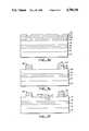
- a process in accordance with our inventionbegins with the step of forming a first epitaxial layer 12 on a semiconductor substrate 10 (FIG. 3a).
- semiconductor substrate 10is semi-insulating gallium arsenide (Although the discussion below describes a process in accordance with our invention for forming a gallium arsenide transistor, other semiconductor materials such as silicon can also be used.)
- Epitaxial layer 12is formed with a vapor phase epitaxy process which uses arsine and liquid gallium as the reactant sources to grow epitaxial layer 12.
- Epitaxial layer 12is typically between 0.5 and 150 microns thick. Preferably, epitaxial layer 12 is between 3 and 5 microns thick.
- Epitaxial layer 12is grown at a rate between 0.1 and 0.5 microns/minute, and the growth temperature is typically between 600 and 750° C. Preferably, the growth rate is approximately 3 microns/minute and the growth temperature is between about 725 and 730° C.
- a P doped region 14is formed in first epitaxial layer 12.
- region 14is formed by implanting ions such as beryllium into epitaxial layer 12 at a nonchanneling angle.
- a nonchanneling angleis an angle that is not parallel to any of the semiconductor crystal axes. Ions implanted at a nonchanneling angle are thus not permitted to pass through large distances within the semiconductor lattice, but instead lodge in the lattice in accordance with a known distribution.
- the implant dosageis typically between 3 ⁇ 10 11 and 5 ⁇ 10 12 /cm 2 and the implant energy is between 10 and 400 KEV. Preferably, the dosage is about 6 ⁇ 10 11 /cm 2 and the implant energy is about 50 KEV.
- P doped region 14prevents electrons from a subsequently formed channel region from flowing far from a subsequently formed transistor gate.
- epitaxial layer 16is grown on first epitaxial layer 12 to a thickness between 0 and 1 micron.
- epitaxial layer 16is 0.1 microns thick.
- Epitaxial layer 16serves as a buffer region between a subsequently formed N type epitaxial layer and P doped region 14.
- epitaxial layer 16is highly desirable, and minimizes the impurity concentration at the bottom of the transistor channel.
- an N type epitaxial layer 18is grown on epitaxial layer 16.
- Epitaxial layer 18is typically between 0.02 and 2 microns thick. Preferably, epitaxial layer 18 is between about 0.2 and 0.5 microns thick.
- the growth rate for epitaxial layers 16 and 18is typically between 10 and 10,000 ⁇ /minute and the growth temperature is between 600 and 750° C. Preferably, the growth rate is between approximately 300 and 500 ⁇ /minute and the growth temperature is between 725 and 730° C.
- the dopant in N type epitaxial layer 18is typically sulfur, silicon, or tellurium. Layer 18 has a dopant concentration sufficient to provide a carrier concentration between 1 ⁇ 10 17 /cc and 5 ⁇ 10 18 /cc.
- epitaxial layer 18is chemically etched to achieve a sheet conductivity between 1.6 and 5.0 millimhos.
- the sheet resistance of a layerdepends in part on its thickness.
- the sheet resistance of layer 18is raised to a desired value.
- ohmic source and drain contactsare then formed on epitaxial layer 18.
- thisis done by covering epitaxial layer 18 with a photoresist layer 19 and patterning the photoresist layer to expose the portions of layer 18 where source and drain contacts are to be formed.
- photoresist layer 19 and the exposed portions of epitaxial layer 18are covered with a layer 20 of gold-germanium alloy, a nickel layer 21, and a gold layer 22, in that order, e.g., by sputtering or evaporation.
- the remaining portions of photoresist layer 19are then removed along with the metal lying thereon, thereby leaving metal source and drain contacts 23 and 24 (FIG. 3e).
- metal contacts 23 and 24each comprise a gold-germanium layer, a nickel layer, and a gold layer.
- the waferis then heated to about 450° C. for approximately 30 seconds, which causes part of the gold-germanium layer within contacts 23 and 24 to alloy with and ohmically contact N type epitaxial layer 18.
- the portion of epitaxial layer 18 where a gate is to be formedis then etched using a conventional technique. This is done by covering the wafer with a second photoresist layer (not shown), patterning the photoresist to expose the part of epitaxial layer 18 where gate 26 (FIG. 3f) is to be formed, and etching a portion of the exposed part of epitaxial layer 18 in a conventional manner.
- the exposed portion of epitaxial layer 18is etched with a solution of water, H 2 O 2 , and NH 4 OH.
- metal gate 26is formed, e.g., by sputtering a refractory metal such as a titanium tungsten alloy onto the wafer and a gold layer onto the titanium tungsten layer.
- a refractory metalsuch as a titanium tungsten alloy
- the remaining photoresistis then removed from the wafer in a conventional manner along with the metal deposited thereon, thereby leaving gate 26, which includes a titanium-tungsten layer 28 and a gold layer 30.
- contacts 23 and 24are formed before gate 26, in other embodiments gate 26 is formed before contacts 23 and 24.
- contacts 23 and 24 and gate 26can be patterned using processes other than the above-described lift process. For example, contacts 23 and 24 can be patterned by covering N type epitaxial layer 18 with metal and then selectively etching away undesired portions of the metal.
- FIG. 4illustrates the structure of FIG. 3f including lines 32 indicating the direction of the electrical field.
- the presence of P doped region 14modifies the shape of the electrical field lines and ensures that electrons do not flow far from gate 26. Because of this, the above-mentioned short channel effects are mitigated.
- P doped region 14modifies the shape of electrical field lines 32 is that holes from region 14 tend to recombine with electrons from epitaxial layer 18, thereby forming a negatively charged space charge region which tends to repel electrons.
- P doped region 14is typically very thin so that the above-mentioned recombination renders layer 14 nonconductive. This is done to avoid capacitance between epitaxial layer 18 and P doped region 14, and thereby avoid capacitive coupling between the transistor source and drain. However, in embodiments in which such capacitance is not a concern, P doped region 14 can be arbitrarily thick.
- P doped region 14is epitaxially grown on epitaxial layer 12.
- the dopant usedis carbon, magnesium, beryllium, zinc, or cadmium.
- P doped region 14has a thickness less than about 1 micron, and is preferably less than 0.2 microns. Preferably, P doped region 14 is made as thin as possible.
- the P type dopant concentration in this alternative embodimentdepends upon the thickness of region 14 but should be such that the product of the dopant concentration times the thickness of region 14 exceeds 1 ⁇ 10 11 /cm 2 .
- N doped layer 18can be any channel layer usable for making field effect transistors.
- the various epitaxial layerscan be grown on substrate 10 in a continuous fashion. In such an embodiment, selected dopants are introduced at selected times during the epitaxial growth process, and growth conditions such as temperature are modified at selected times so that layers 12, 14, 16, and 18 are formed having desired characters.
- N doped layer 18is replaced by multilayer channel structures, e.g. a heterostructure such as a HEMT.
- a heterostructureis a Schottky FET in which the channel region includes a plurality of layers of different semiconductor materials.
- a HEMTis a heterostructure FET in which electrons are donated by donors in a high band gap material. The donated electrons flow through adjacent undoped low band gap material to maximize carrier mobility through the transistor channel.
- FIG. 5illustrates an inversion mode transistor constructed in accordance with another embodiment of our invention.
- a layer 34is formed on region 14.
- Layer 34is undoped or lightly doped with P type impurities.
- N type source and drain regions 36 and 38are formed in layer 34, e.g. by ion implantation, and ohmic metal contacts 40 and 42 are formed on regions 36 and 38, respectively.
- a layer 39is formed on a portion of layer 34 and a gate 44 is then formed on layer 39.
- Layer 39is typically epitaxially grown high band-gap material or an insulator, and electrically insulates gate 44 from the underlying semiconductor material. Electrical conduction between regions 36 and 38 is modulated by the electrical potential of gate 44. Region 14 tends to confine current carriers near gate 44 as in the previous embodiment.
- semiconductor materials other than gallium arsenidecan be used, e.g. silicon, InP, GaInAs, GaInP, AlGaAs, GaAsP, GaInAsP, etc.
- the process of the present inventioncan be used to manufacture devices other than Schottky FETs, e.g., JFETs and MOSFETs.
- the process of the present inventioncan be used to form both P channel and N channel transistors.
- the process of the present inventioncan also be used to form enhancement mode and depletion mode transistors. Accordingly, all such changes come within the present invention.
Landscapes
- Junction Field-Effect Transistors (AREA)
Abstract
Description
Claims (12)
Priority Applications (1)
| Application Number | Priority Date | Filing Date | Title |
|---|---|---|---|
| US06/911,270US4788156A (en) | 1986-09-24 | 1986-09-24 | Subchannel doping to reduce short-gate effects in field effect transistors |
Applications Claiming Priority (1)
| Application Number | Priority Date | Filing Date | Title |
|---|---|---|---|
| US06/911,270US4788156A (en) | 1986-09-24 | 1986-09-24 | Subchannel doping to reduce short-gate effects in field effect transistors |
Publications (1)
| Publication Number | Publication Date |
|---|---|
| US4788156Atrue US4788156A (en) | 1988-11-29 |
Family
ID=25430001
Family Applications (1)
| Application Number | Title | Priority Date | Filing Date |
|---|---|---|---|
| US06/911,270Expired - LifetimeUS4788156A (en) | 1986-09-24 | 1986-09-24 | Subchannel doping to reduce short-gate effects in field effect transistors |
Country Status (1)
| Country | Link |
|---|---|
| US (1) | US4788156A (en) |
Cited By (33)
| Publication number | Priority date | Publication date | Assignee | Title |
|---|---|---|---|---|
| US5141879A (en)* | 1989-08-28 | 1992-08-25 | Herbert Goronkin | Method of fabricating a FET having a high trap concentration interface layer |
| US5406099A (en)* | 1992-02-25 | 1995-04-11 | Sony Corporation | High electron mobility transistor |
| US5610085A (en)* | 1993-11-29 | 1997-03-11 | Texas Instruments Incorporated | Method of making a vertical FET using epitaxial overgrowth |
| US5701019A (en)* | 1993-03-12 | 1997-12-23 | Hitachi, Ltd. | Semiconductor device having first and second stacked semiconductor layers, with electrical contact to the first semiconductor layer |
| US6482330B1 (en) | 1999-10-01 | 2002-11-19 | Komag, Inc. | Method for manufacturing a data storage card |
| US20030102482A1 (en)* | 2001-12-03 | 2003-06-05 | Saxler Adam William | Strain balanced nitride heterojunction transistors and methods of fabricating strain balanced nitride heterojunction transistors |
| US20030157776A1 (en)* | 2000-12-01 | 2003-08-21 | Smith Richard Peter | Methods of fabricating aluminum gallium nitride/gallium nitride high electron mobility transistors having a gate contact on a gallium nitride based cap segment |
| US20030178654A1 (en)* | 1999-06-02 | 2003-09-25 | Thornton Trevor J. | Complementary Schottky junction transistors and methods of forming the same |
| US20040061129A1 (en)* | 2002-07-16 | 2004-04-01 | Saxler Adam William | Nitride-based transistors and methods of fabrication thereof using non-etched contact recesses |
| US20050184343A1 (en)* | 1999-06-02 | 2005-08-25 | Thornton Trevor J. | MESFETs integrated with MOSFETs on common substrate and methods of forming the same |
| US20050258451A1 (en)* | 2004-05-20 | 2005-11-24 | Saxler Adam W | Methods of fabricating nitride-based transistors having regrown ohmic contact regions and nitride-based transistors having regrown ohmic contact regions |
| US20050258450A1 (en)* | 2004-05-20 | 2005-11-24 | Saxler Adam W | Semiconductor devices having a hybrid channel layer, current aperture transistors and methods of fabricating same |
| US20060017064A1 (en)* | 2004-07-26 | 2006-01-26 | Saxler Adam W | Nitride-based transistors having laterally grown active region and methods of fabricating same |
| US20060019435A1 (en)* | 2004-07-23 | 2006-01-26 | Scott Sheppard | Methods of fabricating nitride-based transistors with a cap layer and a recessed gate |
| US7045404B2 (en) | 2004-01-16 | 2006-05-16 | Cree, Inc. | Nitride-based transistors with a protective layer and a low-damage recess and methods of fabrication thereof |
| US20060108606A1 (en)* | 2004-11-23 | 2006-05-25 | Saxler Adam W | Cap layers and/or passivation layers for nitride-based transistors, transistor structures and methods of fabricating same |
| US20060118809A1 (en)* | 2004-12-06 | 2006-06-08 | Primit Parikh | High power density and/or linearity transistors |
| US20060118823A1 (en)* | 2004-12-06 | 2006-06-08 | Primit Parikh | Field effect transistors (FETs) having multi-watt output power at millimeter-wave frequencies |
| US20060208280A1 (en)* | 2005-03-15 | 2006-09-21 | Smith Richard P | Group III nitride field effect transistors (FETS) capable of withstanding high temperature reverse bias test conditions |
| US20060226412A1 (en)* | 2005-04-11 | 2006-10-12 | Saxler Adam W | Thick semi-insulating or insulating epitaxial gallium nitride layers and devices incorporating same |
| US20060226413A1 (en)* | 2005-04-11 | 2006-10-12 | Saxler Adam W | Composite substrates of conductive and insulating or semi-insulating group III-nitrides for group III-nitride devices |
| US20060244010A1 (en)* | 2005-04-29 | 2006-11-02 | Saxler Adam W | Aluminum free group III-nitride based high electron mobility transistors and methods of fabricating same |
| US20060244011A1 (en)* | 2005-04-29 | 2006-11-02 | Saxler Adam W | Binary group III-nitride based high electron mobility transistors and methods of fabricating same |
| US20070018198A1 (en)* | 2005-07-20 | 2007-01-25 | Brandes George R | High electron mobility electronic device structures comprising native substrates and methods for making the same |
| US7170111B2 (en) | 2004-02-05 | 2007-01-30 | Cree, Inc. | Nitride heterojunction transistors having charge-transfer induced energy barriers and methods of fabricating the same |
| US20070164315A1 (en)* | 2004-11-23 | 2007-07-19 | Cree, Inc. | Cap Layers Including Aluminum Nitride for Nitride-Based Transistors and Methods of Fabricating Same |
| US7592211B2 (en) | 2006-01-17 | 2009-09-22 | Cree, Inc. | Methods of fabricating transistors including supported gate electrodes |
| US7612390B2 (en) | 2004-02-05 | 2009-11-03 | Cree, Inc. | Heterojunction transistors including energy barriers |
| US20100068855A1 (en)* | 2004-01-16 | 2010-03-18 | Cree, Inc. | Group III nitride semiconductor devices with silicon nitride layers and methods of manufacturing such devices |
| US7709269B2 (en) | 2006-01-17 | 2010-05-04 | Cree, Inc. | Methods of fabricating transistors including dielectrically-supported gate electrodes |
| US8823057B2 (en) | 2006-11-06 | 2014-09-02 | Cree, Inc. | Semiconductor devices including implanted regions for providing low-resistance contact to buried layers and related devices |
| US9299821B2 (en) | 2010-06-23 | 2016-03-29 | Cornell University | Gated III-V semiconductor structure and method |
| US9331192B2 (en) | 2005-06-29 | 2016-05-03 | Cree, Inc. | Low dislocation density group III nitride layers on silicon carbide substrates and methods of making the same |
Citations (4)
| Publication number | Priority date | Publication date | Assignee | Title |
|---|---|---|---|---|
| US4377030A (en)* | 1980-02-15 | 1983-03-22 | Siemens Aktiengesellschaft | Metallization of selectively implanted AIII -BV compound semiconductors |
| US4422087A (en)* | 1980-06-03 | 1983-12-20 | Xerox Corporation | Self-aligned short channel MESFET |
| US4503599A (en)* | 1982-01-29 | 1985-03-12 | Hitachi, Ltd. | Method of fabricating field effect transistors |
| US4642879A (en)* | 1982-11-29 | 1987-02-17 | Fujitsu Limited | Method of making self-aligned FET using GaAs substrate and spatially controlled implanted channel region |
- 1986
- 1986-09-24USUS06/911,270patent/US4788156A/ennot_activeExpired - Lifetime
Patent Citations (4)
| Publication number | Priority date | Publication date | Assignee | Title |
|---|---|---|---|---|
| US4377030A (en)* | 1980-02-15 | 1983-03-22 | Siemens Aktiengesellschaft | Metallization of selectively implanted AIII -BV compound semiconductors |
| US4422087A (en)* | 1980-06-03 | 1983-12-20 | Xerox Corporation | Self-aligned short channel MESFET |
| US4503599A (en)* | 1982-01-29 | 1985-03-12 | Hitachi, Ltd. | Method of fabricating field effect transistors |
| US4642879A (en)* | 1982-11-29 | 1987-02-17 | Fujitsu Limited | Method of making self-aligned FET using GaAs substrate and spatially controlled implanted channel region |
Non-Patent Citations (4)
| Title |
|---|
| Takada et al., "A 2 Gb/s Throughput GaAs Digital Time Switch LSI Using LSCFL", IEEE 1985 Microwave and Millimeter Wave Monolithic Circuit Symposium at St. Louis, MO, pgs. 22-26. |
| Takada et al., A 2 Gb/s Throughput GaAs Digital Time Switch LSI Using LSCFL , IEEE 1985 Microwave and Millimeter Wave Monolithic Circuit Symposium at St. Louis, MO, pgs. 22 26.* |
| Yamasaki et al., "Below 10 ps/Gate Operation With Buried p-Layer SAINT FETS", published in Electronics Letters on Dec. 6, 1984, pp. 1029-1031. |
| Yamasaki et al., Below 10 ps/Gate Operation With Buried p Layer SAINT FETS , published in Electronics Letters on Dec. 6, 1984, pp. 1029 1031.* |
Cited By (79)
| Publication number | Priority date | Publication date | Assignee | Title |
|---|---|---|---|---|
| US5141879A (en)* | 1989-08-28 | 1992-08-25 | Herbert Goronkin | Method of fabricating a FET having a high trap concentration interface layer |
| US5406099A (en)* | 1992-02-25 | 1995-04-11 | Sony Corporation | High electron mobility transistor |
| US5701019A (en)* | 1993-03-12 | 1997-12-23 | Hitachi, Ltd. | Semiconductor device having first and second stacked semiconductor layers, with electrical contact to the first semiconductor layer |
| US5610085A (en)* | 1993-11-29 | 1997-03-11 | Texas Instruments Incorporated | Method of making a vertical FET using epitaxial overgrowth |
| US6864131B2 (en)* | 1999-06-02 | 2005-03-08 | Arizona State University | Complementary Schottky junction transistors and methods of forming the same |
| US7589007B2 (en) | 1999-06-02 | 2009-09-15 | Arizona Board Of Regents For And On Behalf Of Arizona State University | MESFETs integrated with MOSFETs on common substrate and methods of forming the same |
| US20030178654A1 (en)* | 1999-06-02 | 2003-09-25 | Thornton Trevor J. | Complementary Schottky junction transistors and methods of forming the same |
| US6987292B2 (en) | 1999-06-02 | 2006-01-17 | Arizona State University | Schottky junction transistors and complementary circuits including the same |
| US20050184343A1 (en)* | 1999-06-02 | 2005-08-25 | Thornton Trevor J. | MESFETs integrated with MOSFETs on common substrate and methods of forming the same |
| US20040256633A1 (en)* | 1999-06-02 | 2004-12-23 | Thornton Trevor J. | Schottky junction transistors and complementary circuits including the same |
| US6482330B1 (en) | 1999-10-01 | 2002-11-19 | Komag, Inc. | Method for manufacturing a data storage card |
| US20030157776A1 (en)* | 2000-12-01 | 2003-08-21 | Smith Richard Peter | Methods of fabricating aluminum gallium nitride/gallium nitride high electron mobility transistors having a gate contact on a gallium nitride based cap segment |
| US6777278B2 (en)* | 2000-12-01 | 2004-08-17 | Cree, Inc. | Methods of fabricating aluminum gallium nitride/gallium nitride high electron mobility transistors having a gate contact on a gallium nitride based cap segment |
| US20030102482A1 (en)* | 2001-12-03 | 2003-06-05 | Saxler Adam William | Strain balanced nitride heterojunction transistors and methods of fabricating strain balanced nitride heterojunction transistors |
| US8153515B2 (en) | 2001-12-03 | 2012-04-10 | Cree, Inc. | Methods of fabricating strain balanced nitride heterojunction transistors |
| US20060121682A1 (en)* | 2001-12-03 | 2006-06-08 | Cree, Inc. | Strain balanced nitride heterojunction transistors and methods of fabricating strain balanced nitride heterojunction transistors |
| US7030428B2 (en) | 2001-12-03 | 2006-04-18 | Cree, Inc. | Strain balanced nitride heterojunction transistors |
| US7550784B2 (en) | 2002-07-16 | 2009-06-23 | Cree, Inc. | Nitride-based transistors and methods of fabrication thereof using non-etched contact recesses |
| US6982204B2 (en) | 2002-07-16 | 2006-01-03 | Cree, Inc. | Nitride-based transistors and methods of fabrication thereof using non-etched contact recesses |
| US20060006435A1 (en)* | 2002-07-16 | 2006-01-12 | Saxler Adam W | Nitride-based transistors and methods of fabrication thereof using non-etched contact recesses |
| US20040061129A1 (en)* | 2002-07-16 | 2004-04-01 | Saxler Adam William | Nitride-based transistors and methods of fabrication thereof using non-etched contact recesses |
| US11316028B2 (en) | 2004-01-16 | 2022-04-26 | Wolfspeed, Inc. | Nitride-based transistors with a protective layer and a low-damage recess |
| US7045404B2 (en) | 2004-01-16 | 2006-05-16 | Cree, Inc. | Nitride-based transistors with a protective layer and a low-damage recess and methods of fabrication thereof |
| US20110140123A1 (en)* | 2004-01-16 | 2011-06-16 | Sheppard Scott T | Nitride-Based Transistors With a Protective Layer and a Low-Damage Recess |
| US20110136305A1 (en)* | 2004-01-16 | 2011-06-09 | Adam William Saxler | Group III Nitride Semiconductor Devices with Silicon Nitride Layers and Methods of Manufacturing Such Devices |
| US7906799B2 (en) | 2004-01-16 | 2011-03-15 | Cree, Inc. | Nitride-based transistors with a protective layer and a low-damage recess |
| US7901994B2 (en) | 2004-01-16 | 2011-03-08 | Cree, Inc. | Methods of manufacturing group III nitride semiconductor devices with silicon nitride layers |
| US8481376B2 (en) | 2004-01-16 | 2013-07-09 | Cree, Inc. | Group III nitride semiconductor devices with silicon nitride layers and methods of manufacturing such devices |
| US20100068855A1 (en)* | 2004-01-16 | 2010-03-18 | Cree, Inc. | Group III nitride semiconductor devices with silicon nitride layers and methods of manufacturing such devices |
| US20060255366A1 (en)* | 2004-01-16 | 2006-11-16 | Sheppard Scott T | Nitride-based transistors with a protective layer and a low-damage recess |
| US7612390B2 (en) | 2004-02-05 | 2009-11-03 | Cree, Inc. | Heterojunction transistors including energy barriers |
| US9035354B2 (en) | 2004-02-05 | 2015-05-19 | Cree, Inc. | Heterojunction transistors having barrier layer bandgaps greater than channel layer bandgaps and related methods |
| US7170111B2 (en) | 2004-02-05 | 2007-01-30 | Cree, Inc. | Nitride heterojunction transistors having charge-transfer induced energy barriers and methods of fabricating the same |
| US7432142B2 (en) | 2004-05-20 | 2008-10-07 | Cree, Inc. | Methods of fabricating nitride-based transistors having regrown ohmic contact regions |
| US20050258450A1 (en)* | 2004-05-20 | 2005-11-24 | Saxler Adam W | Semiconductor devices having a hybrid channel layer, current aperture transistors and methods of fabricating same |
| US7084441B2 (en) | 2004-05-20 | 2006-08-01 | Cree, Inc. | Semiconductor devices having a hybrid channel layer, current aperture transistors and methods of fabricating same |
| US20050258451A1 (en)* | 2004-05-20 | 2005-11-24 | Saxler Adam W | Methods of fabricating nitride-based transistors having regrown ohmic contact regions and nitride-based transistors having regrown ohmic contact regions |
| US7479669B2 (en) | 2004-05-20 | 2009-01-20 | Cree, Inc. | Current aperture transistors and methods of fabricating same |
| US20100140664A1 (en)* | 2004-07-23 | 2010-06-10 | Scott Sheppard | Methods of Fabricating Nitride-Based Transistors with a Cap Layer and a Recessed Gate and Related Devices |
| US9666707B2 (en) | 2004-07-23 | 2017-05-30 | Cree, Inc. | Nitride-based transistors with a cap layer and a recessed gate |
| US20070254418A1 (en)* | 2004-07-23 | 2007-11-01 | Scott Sheppard | Methods of fabricating nitride-based transistors with a cap layer and a recessed gate |
| US7678628B2 (en) | 2004-07-23 | 2010-03-16 | Cree, Inc. | Methods of fabricating nitride-based transistors with a cap layer and a recessed gate |
| US20060019435A1 (en)* | 2004-07-23 | 2006-01-26 | Scott Sheppard | Methods of fabricating nitride-based transistors with a cap layer and a recessed gate |
| US7238560B2 (en) | 2004-07-23 | 2007-07-03 | Cree, Inc. | Methods of fabricating nitride-based transistors with a cap layer and a recessed gate |
| US20100012952A1 (en)* | 2004-07-26 | 2010-01-21 | Adam William Saxler | Nitride-Based Transistors Having Laterally Grown Active Region and Methods of Fabricating Same |
| US8946777B2 (en) | 2004-07-26 | 2015-02-03 | Cree, Inc. | Nitride-based transistors having laterally grown active region and methods of fabricating same |
| US20060017064A1 (en)* | 2004-07-26 | 2006-01-26 | Saxler Adam W | Nitride-based transistors having laterally grown active region and methods of fabricating same |
| US7709859B2 (en) | 2004-11-23 | 2010-05-04 | Cree, Inc. | Cap layers including aluminum nitride for nitride-based transistors |
| US9166033B2 (en) | 2004-11-23 | 2015-10-20 | Cree, Inc. | Methods of passivating surfaces of wide bandgap semiconductor devices |
| US20060108606A1 (en)* | 2004-11-23 | 2006-05-25 | Saxler Adam W | Cap layers and/or passivation layers for nitride-based transistors, transistor structures and methods of fabricating same |
| US20090042345A1 (en)* | 2004-11-23 | 2009-02-12 | Cree, Inc. | Methods of Fabricating Transistors Having Buried N-Type and P-Type Regions Beneath the Source Region |
| US20070164315A1 (en)* | 2004-11-23 | 2007-07-19 | Cree, Inc. | Cap Layers Including Aluminum Nitride for Nitride-Based Transistors and Methods of Fabricating Same |
| US7456443B2 (en) | 2004-11-23 | 2008-11-25 | Cree, Inc. | Transistors having buried n-type and p-type regions beneath the source region |
| US7161194B2 (en) | 2004-12-06 | 2007-01-09 | Cree, Inc. | High power density and/or linearity transistors |
| US20060118823A1 (en)* | 2004-12-06 | 2006-06-08 | Primit Parikh | Field effect transistors (FETs) having multi-watt output power at millimeter-wave frequencies |
| US20060118809A1 (en)* | 2004-12-06 | 2006-06-08 | Primit Parikh | High power density and/or linearity transistors |
| US7355215B2 (en) | 2004-12-06 | 2008-04-08 | Cree, Inc. | Field effect transistors (FETs) having multi-watt output power at millimeter-wave frequencies |
| US8803198B2 (en) | 2005-03-15 | 2014-08-12 | Cree, Inc. | Group III nitride field effect transistors (FETS) capable of withstanding high temperature reverse bias test conditions |
| US7465967B2 (en) | 2005-03-15 | 2008-12-16 | Cree, Inc. | Group III nitride field effect transistors (FETS) capable of withstanding high temperature reverse bias test conditions |
| US8212289B2 (en) | 2005-03-15 | 2012-07-03 | Cree, Inc. | Group III nitride field effect transistors (FETS) capable of withstanding high temperature reverse bias test conditions |
| US20060208280A1 (en)* | 2005-03-15 | 2006-09-21 | Smith Richard P | Group III nitride field effect transistors (FETS) capable of withstanding high temperature reverse bias test conditions |
| US20060226412A1 (en)* | 2005-04-11 | 2006-10-12 | Saxler Adam W | Thick semi-insulating or insulating epitaxial gallium nitride layers and devices incorporating same |
| US9224596B2 (en) | 2005-04-11 | 2015-12-29 | Cree, Inc. | Methods of fabricating thick semi-insulating or insulating epitaxial gallium nitride layers |
| US20060226413A1 (en)* | 2005-04-11 | 2006-10-12 | Saxler Adam W | Composite substrates of conductive and insulating or semi-insulating group III-nitrides for group III-nitride devices |
| US8575651B2 (en) | 2005-04-11 | 2013-11-05 | Cree, Inc. | Devices having thick semi-insulating epitaxial gallium nitride layer |
| US7626217B2 (en) | 2005-04-11 | 2009-12-01 | Cree, Inc. | Composite substrates of conductive and insulating or semi-insulating group III-nitrides for group III-nitride devices |
| US7544963B2 (en) | 2005-04-29 | 2009-06-09 | Cree, Inc. | Binary group III-nitride based high electron mobility transistors |
| US20060244010A1 (en)* | 2005-04-29 | 2006-11-02 | Saxler Adam W | Aluminum free group III-nitride based high electron mobility transistors and methods of fabricating same |
| US20060244011A1 (en)* | 2005-04-29 | 2006-11-02 | Saxler Adam W | Binary group III-nitride based high electron mobility transistors and methods of fabricating same |
| US7615774B2 (en) | 2005-04-29 | 2009-11-10 | Cree.Inc. | Aluminum free group III-nitride based high electron mobility transistors |
| US9331192B2 (en) | 2005-06-29 | 2016-05-03 | Cree, Inc. | Low dislocation density group III nitride layers on silicon carbide substrates and methods of making the same |
| US20070018198A1 (en)* | 2005-07-20 | 2007-01-25 | Brandes George R | High electron mobility electronic device structures comprising native substrates and methods for making the same |
| US7709269B2 (en) | 2006-01-17 | 2010-05-04 | Cree, Inc. | Methods of fabricating transistors including dielectrically-supported gate electrodes |
| US7592211B2 (en) | 2006-01-17 | 2009-09-22 | Cree, Inc. | Methods of fabricating transistors including supported gate electrodes |
| US7960756B2 (en) | 2006-01-17 | 2011-06-14 | Cree, Inc. | Transistors including supported gate electrodes |
| US8049252B2 (en) | 2006-01-17 | 2011-11-01 | Cree, Inc. | Methods of fabricating transistors including dielectrically-supported gate electrodes and related devices |
| US8823057B2 (en) | 2006-11-06 | 2014-09-02 | Cree, Inc. | Semiconductor devices including implanted regions for providing low-resistance contact to buried layers and related devices |
| US9984881B2 (en) | 2006-11-06 | 2018-05-29 | Cree, Inc. | Methods of fabricating semiconductor devices including implanted regions for providing low-resistance contact to buried layers and related devices |
| US9299821B2 (en) | 2010-06-23 | 2016-03-29 | Cornell University | Gated III-V semiconductor structure and method |
Similar Documents
| Publication | Publication Date | Title |
|---|---|---|
| US4788156A (en) | Subchannel doping to reduce short-gate effects in field effect transistors | |
| US6573129B2 (en) | Gate electrode formation in double-recessed transistor by two-step etching | |
| US4711858A (en) | Method of fabricating a self-aligned metal-semiconductor FET having an insulator spacer | |
| US5411914A (en) | III-V based integrated circuits having low temperature growth buffer or passivation layers | |
| US4908325A (en) | Method of making heterojunction transistors with wide band-gap stop etch layer | |
| EP0114962A2 (en) | Double heterojunction field effect transistors | |
| WO2001061733A2 (en) | Double recessed transistor | |
| JPH10177953A (en) | Monolithic microwave integrated circuit including high electron mobility transistor and heterojunction bipolar transistor and method of manufacturing the same by single growth processing | |
| JPS634955B2 (en) | ||
| JPH0324782B2 (en) | ||
| US5098853A (en) | Self-aligned, planar heterojunction bipolar transistor and method of forming the same | |
| US4771324A (en) | Heterojunction field effect device having an implanted region within a device channel | |
| EP0130774B1 (en) | Process for fabricating bipolar transistor | |
| JPS61188966A (en) | Manufacturing method for high-speed semiconductor devices | |
| US5413947A (en) | Method for manufacturing a semiconductor device with an epitaxial void | |
| GB2239557A (en) | High electron mobility transistors | |
| EP0437702B1 (en) | Semiconductor integrated circuit of compound semiconductor devices comprising isolation regions and method of making the same | |
| JPH02111073A (en) | Insulated gate field effect transistor and its integrated circuit device | |
| JP3304343B2 (en) | Field effect transistor | |
| GB2151078A (en) | Semiconductor devices | |
| JPS6143443A (en) | Manufacture of semiconductor device | |
| JP2503594B2 (en) | Semiconductor integrated device and manufacturing method thereof | |
| CA1196111A (en) | Ingaas field effect transistor | |
| JPH0429225B2 (en) | ||
| JPH0810701B2 (en) | Method for manufacturing junction field effect transistor |
Legal Events
| Date | Code | Title | Description |
|---|---|---|---|
| AS | Assignment | Owner name:MICROWAVE TECHNOLOGY, INC., 4268 SOLAR WAY, FREMON Free format text:ASSIGNMENT OF ASSIGNORS INTEREST.;ASSIGNORS:STONEHAM, EDWARD B.;OMORI, MASAHIRO;HERBIG, ARTHUR D.;REEL/FRAME:004661/0831 Effective date:19870121 Owner name:MICROWAVE TECHNOLOGY, INC., A CORP OF CA., CALIFOR Free format text:ASSIGNMENT OF ASSIGNORS INTEREST;ASSIGNORS:STONEHAM, EDWARD B.;OMORI, MASAHIRO;HERBIG, ARTHUR D.;REEL/FRAME:004661/0831 Effective date:19870121 | |
| FEPP | Fee payment procedure | Free format text:PAYOR NUMBER ASSIGNED (ORIGINAL EVENT CODE: ASPN); ENTITY STATUS OF PATENT OWNER: SMALL ENTITY | |
| REMI | Maintenance fee reminder mailed | ||
| FPAY | Fee payment | Year of fee payment:4 | |
| SULP | Surcharge for late payment | ||
| REMI | Maintenance fee reminder mailed | ||
| REIN | Reinstatement after maintenance fee payment confirmed | ||
| FP | Lapsed due to failure to pay maintenance fee | Effective date:19961204 | |
| FEPP | Fee payment procedure | Free format text:PETITION RELATED TO MAINTENANCE FEES FILED (ORIGINAL EVENT CODE: PMFP); ENTITY STATUS OF PATENT OWNER: SMALL ENTITY | |
| FEPP | Fee payment procedure | Free format text:PETITION RELATED TO MAINTENANCE FEES GRANTED (ORIGINAL EVENT CODE: PMFG); ENTITY STATUS OF PATENT OWNER: SMALL ENTITY | |
| FPAY | Fee payment | Year of fee payment:8 | |
| SULP | Surcharge for late payment | ||
| STCF | Information on status: patent grant | Free format text:PATENTED CASE | |
| PRDP | Patent reinstated due to the acceptance of a late maintenance fee | Effective date:19980424 | |
| AS | Assignment | Owner name:SILICON VALLEY BANK, CALIFORNIA Free format text:SECURITY AGREEMENT;ASSIGNOR:MICROWAVE TECHNOLOGY, INC.;REEL/FRAME:014090/0700 Effective date:20010703 | |
| AS | Assignment | Owner name:MICROWAVE TECHNOLOGY, INC., CALIFORNIA Free format text:RELEASE BY SECURED PARTY;ASSIGNOR:SILICON VALLEY BANK;REEL/FRAME:064580/0552 Effective date:20230612 |