US4783719A - Test connector for electrical devices - Google Patents
Test connector for electrical devicesDownload PDFInfo
- Publication number
- US4783719A US4783719AUS07/005,054US505487AUS4783719AUS 4783719 AUS4783719 AUS 4783719AUS 505487 AUS505487 AUS 505487AUS 4783719 AUS4783719 AUS 4783719A
- Authority
- US
- United States
- Prior art keywords
- film
- conductor lines
- interface board
- die
- pads
- Prior art date
- Legal status (The legal status is an assumption and is not a legal conclusion. Google has not performed a legal analysis and makes no representation as to the accuracy of the status listed.)
- Expired - Lifetime
Links
- 238000012360testing methodMethods0.000titleabstractdescription25
- 239000004020conductorSubstances0.000claimsabstractdescription39
- 238000003780insertionMethods0.000claimsdescription5
- 230000037431insertionEffects0.000claimsdescription5
- 239000004642PolyimideSubstances0.000claimsdescription3
- 229920001721polyimidePolymers0.000claimsdescription3
- 239000000463materialSubstances0.000claims2
- 239000012858resilient materialSubstances0.000claims2
- 238000010438heat treatmentMethods0.000claims1
- 239000000969carrierSubstances0.000abstractdescription10
- 238000000034methodMethods0.000abstractdescription3
- 229910000679solderInorganic materials0.000abstractdescription3
- RYGMFSIKBFXOCR-UHFFFAOYSA-NCopperChemical compound[Cu]RYGMFSIKBFXOCR-UHFFFAOYSA-N0.000description9
- 229910052802copperInorganic materials0.000description9
- 239000010949copperSubstances0.000description9
- 229920002120photoresistant polymerPolymers0.000description9
- LQBJWKCYZGMFEV-UHFFFAOYSA-Nlead tinChemical compound[Sn].[Pb]LQBJWKCYZGMFEV-UHFFFAOYSA-N0.000description8
- 230000002093peripheral effectEffects0.000description7
- 239000000523sampleSubstances0.000description3
- 238000005530etchingMethods0.000description2
- 230000006870functionEffects0.000description2
- 239000012212insulatorSubstances0.000description2
- 238000004519manufacturing processMethods0.000description2
- ISWSIDIOOBJBQZ-UHFFFAOYSA-Nphenol groupChemical groupC1(=CC=CC=C1)OISWSIDIOOBJBQZ-UHFFFAOYSA-N0.000description2
- 229920003223poly(pyromellitimide-1,4-diphenyl ether)Polymers0.000description2
- 239000000919ceramicSubstances0.000description1
- BGTFCAQCKWKTRL-YDEUACAXSA-Nchembl1095986Chemical compoundC1[C@@H](N)[C@@H](O)[C@H](C)O[C@H]1O[C@@H]([C@H]1C(N[C@H](C2=CC(O)=CC(O[C@@H]3[C@H]([C@@H](O)[C@H](O)[C@@H](CO)O3)O)=C2C=2C(O)=CC=C(C=2)[C@@H](NC(=O)[C@@H]2NC(=O)[C@@H]3C=4C=C(C(=C(O)C=4)C)OC=4C(O)=CC=C(C=4)[C@@H](N)C(=O)N[C@@H](C(=O)N3)[C@H](O)C=3C=CC(O4)=CC=3)C(=O)N1)C(O)=O)=O)C(C=C1)=CC=C1OC1=C(O[C@@H]3[C@H]([C@H](O)[C@@H](O)[C@H](CO[C@@H]5[C@H]([C@@H](O)[C@H](O)[C@@H](C)O5)O)O3)O[C@@H]3[C@H]([C@@H](O)[C@H](O)[C@@H](CO)O3)O[C@@H]3[C@H]([C@H](O)[C@@H](CO)O3)O)C4=CC2=C1BGTFCAQCKWKTRL-YDEUACAXSA-N0.000description1
- 230000001351cycling effectEffects0.000description1
- 238000010586diagramMethods0.000description1
- 238000009713electroplatingMethods0.000description1
- PCHJSUWPFVWCPO-UHFFFAOYSA-NgoldChemical compound[Au]PCHJSUWPFVWCPO-UHFFFAOYSA-N0.000description1
- 239000010931goldSubstances0.000description1
- 229910052737goldInorganic materials0.000description1
- 239000011810insulating materialSubstances0.000description1
- 230000000873masking effectEffects0.000description1
- 239000002184metalSubstances0.000description1
- 229910052751metalInorganic materials0.000description1
- 238000001465metallisationMethods0.000description1
- 230000001681protective effectEffects0.000description1
- 230000035807sensationEffects0.000description1
- 239000002904solventSubstances0.000description1
- 239000000758substrateSubstances0.000description1
Images


Classifications
- G—PHYSICS
- G01—MEASURING; TESTING
- G01R—MEASURING ELECTRIC VARIABLES; MEASURING MAGNETIC VARIABLES
- G01R1/00—Details of instruments or arrangements of the types included in groups G01R5/00 - G01R13/00 and G01R31/00
- G01R1/02—General constructional details
- G01R1/04—Housings; Supporting members; Arrangements of terminals
- G01R1/0408—Test fixtures or contact fields; Connectors or connecting adaptors; Test clips; Test sockets
- G01R1/0433—Sockets for IC's or transistors
- G01R1/0483—Sockets for un-leaded IC's having matrix type contact fields, e.g. BGA or PGA devices; Sockets for unpackaged, naked chips
Definitions
- the present inventionrelates to text fixtures for conducting electrical testing of electrical devices such as integrated circuit dies and leadless integrated circuit carriers, and more particularly to an improved apparatus for providing electrical connections to such devices without the use of fragile wire fingers or wire bond connections.
- IC diesare formed when a multiple circuit substrate is scribed and cut into individual dies or chips. Each die has a plurality of terminal pads formed on a surface thereof, to which electrical connections are made to connect the IC die into a circuit.
- Leadless integrated circuit (IC or "chip”) carriersare in widespread use for mounting IC dies. These chip carriers typically are fabricated from ceramic, and have a substantially planar configuration, with a plurality of closely spaced contact terminals formed around the external periphery of the carrier. A printed wiring pattern is formed on an upper surface of the chip carrier. The IC die is bonded to a surface of the carrier, with electrical terminal being made between contact pads on the IC die and pad locations on the printed wiring pattern, e.g., by wirebonds. The wiring pattern connects the pad locations to predetermined leadless carrier terminals, typically located on the external periphery of the chip carrier.
- Leadless chip carriersare conventionally soldered onto a printed circuit board, with the peripheral chip terminals soldered at predetermined locations on the board printed wiring diagram.
- test fixtureshave been used which employ wire fingers or wiskers arranged in the peripheral configuration of the carrier to be tested.
- the peripheral contact terminals of the carrierare brought into electrical contact with the wire fingers of the fixture.
- These conventional test fixturesare expensive and the wire fingers are fragile.
- a different fixture configurationis required for each type of device to be tested, since electrical contacts are achieved by the matching of the locations of the wire fingers to the peripheral contact terminal configuration of the chip carrier. Since a typical center-to-center spacing of the carrier contacts is 0.020 inches, with some forty to sixty-odd terminals per side of the carrier, the complexity of the conventional test fixture, with one wire finger or wisker corresponding to each contact terminal on the chip carrier, may be readily appreciated.
- the connector apparatuscomprises a flexible film having a plurality of conductive raised pads formed thereon and extending above the surface of the film in a pattern corresponding to the terminal pattern of the chip carrier, with a plurality of conductor lines connecting to respective ones of the conductive raised pads.
- the connector apparatusalso includes means for resiliently urging the flexible film against the surface of the chip carrier with respective ones of the raised pads aligned with corresponding ones of the chip carrier terminals so that electrical contact is achieved between the carrier terminals and the raised pads of the film.
- the connector apparatusfurther comprises means for electrically connecting to the respective conductive lines formed on the film to provide electrical contact to the chip carrier terminals.
- the connector apparatusis particularly adapted for testing IC dies.
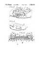
- FIG. 1is a diagrammatic exploded perspective view of a first embodiment of a connector apparatus embodying the present invention.
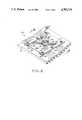
- FIG. 2is a perspective view of the assembled apparatus of FIG. 1.
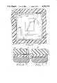
- FIG. 3is an enlarged perspective view of the portion of the flexible film enclosed within phantom circle 3 of FIG. 1 and showing the raised conductive dots formed thereon.
- FIG. 4is a cross-sectional view of the connector apparatus taken along line 4--4 of FIG. 2.
- FIG. 5is a longitudinal sectional view of the connector apparatus taken along line 5--5 of FIG. 4.
- FIG. 6is an enlarged cross-sectional view of the test fixture within the phantom circle 6 of FIG. 4, showing the engagement of a raised pad on the flexible film and a corresponding chip terminal.
- FIG. 7is an enlarged cross-section view of the portion of the connector apparatus within phantom circle 7 of FIG. 4 showing the engagement of a raised pad on the flexible film with a conductor line on an interface board.
- FIG. 8is a perspective view of a second embodiment of a connector apparatus embodying the invention suitable for making electrical connections to an IC die.
- FIG. 9is a cross-sectional view of the connector apparatus of claim 8 taken along line 9--9 of FIG. 8.
- FIG. 10is a top plan view of the flexible film employed with the connector apparatus of FIG. 8.
- Leadless chip carrierssuch as the chip carrier 60 shown in FIG. 1, comprise a plurality of closely spaced terminals 61 extending about the outer periphery 60a of the carrier.
- the terminals 61are wrapped around the external periphery of the chip carrier 60, extending from the top surface 60b along the side periphery surface 60a and to the lower surface 60c of the chip carrier 60.
- the apparatus 10comprises connector fixture 20, top plate 30, flexible film layer 50 and interface board 45.
- Connector fixture 20is fabricated from an insulator such as a paper based phenolic.
- the fixture 20comprises an member having a recessed area 22 formed in its upwardly facing surface 20a.
- the area 22is shaped in the configuration of the outer periphery of the chip carrier 60.
- a resilient layer 25 of high temperature rubber sized to fit into the recessed area 22is also provided.
- the thickness of the resilient layer 25substantially matches the depth of recess 22.
- the top fixture plate 30is also fabricated from an insulator such as a paper base phenolic.
- the top plate 30comprises an open frame defining opening 32, formed in the configuration of the outer periphery of the chip carrier 60.
- the apparatus 10further comprises a flexible film 50 comprises a layer of flexible insulating material, such as the polyimide marketed under the name "Kapton," by E. I. DuPont Company.
- a plurality of conductor lines 54are formed on the surface 50e of layer 50 in a wiring pattern; the conductor lines are terminated at each end by conductive raised pads 52 and 55, respectively.
- the pads 52are disposed to make contact with terminals on the chip carrier 60; the pads 55 are disposed to make contact with conductor lines formed on the interface board 45, as will be described below. While the carrier 60 typically has terminals at all four sides, and the pads 52 are arranged to correspond to the locations of all the carrier terminals, the conductor lines 54 are arranged to connect to pads 55 located on only two sides or ends of the film 50 in this embodiment.
- FIG. 3is an enlarged perspective view of the portion of the film 50 enclosed within phantom circle 3 of FIG. 1, and illustrates the raised pads 55 in greater detail.
- the padshave a diameter of about 0.005 inches, and extend above the surface of the film 50 about 0.001 inches.
- the top plate 30 and fixture plate 20are cooperatively arranged to sandwich the flexible film layer 50 and the test carrier 60 between them as shown in the exploded view of FIG. 1 and in FIG. 2, which show the apparatus in its assembled configuration.
- the fixture plate 20is provided with a pair of opposed spring clips 23a and 23b which pivot about pins 24a and 24b. In the assembled configuration as shown in FIG. 2, the spring clips 23a, 23b are pivoted over the top edge surface of the top plate 30 and snap into corresponding grooves 31a, 31b to secure the assembly of elements 20, 25, 60 and 30 together.
- the fixture plate 20, the resilient layer 25 and the top plate 30provide a means for resiliently urging the flexible film against the lower surface 60c of the chip carrier 60 with the raised pads 52 aligned with corresponding ones of the pad terminals 61 so as to achieve electrical contact therebetween, as shown in FIG. 6.
- the flexibility of the filmallows it to conform to non-planar device contours.
- the apparatus 10further comprises a pair of resilient blocks 35 and 40 fabricated of high temperature rubber.
- the blocks 35 and 40are received in a pair of corresponding recessed regions 21a, 21b formed in lower surface of plate 20, as shown in FIG. 4.
- the ends of the flexible film 50are folded under the fixture 20, as shown in FIGS. 2 and 4, so that the raised pads 55 are facing downwardly. With the pins 65 fitted through the corresponding openings 70 in member 20, holes 72 in member 30 and sprocket openings 53 (FIG. 1) in film 50, this assembly is then urged against the upper surface of the interface board 45.
- a plurality of threaded fasteners 75are inserted though countersunk openings 76 formed in fixture 20 and through corresponding openings 77 formed in interface board 45, and are secured by nuts 78 to draw down securely against board 45 the assembly of the fixture 20 and the film 50.
- a printed wiring patternis defined on the upper surface 45a of board 45, comprising a plurality of conductor lines 46 which are terminated in conductive pads 47.
- the conductor line pattern of the interface board 45is arranged to conform to the respective locations of the raised pads 55 formed on film layer 50 when the ends of the film 50 are folded under the fixture plate 20.
- the blocks 21a and 21bprovide a means of resiliently urging the conductive pads 55 against corresponding conductive pads 47 formed on board 45, as shown in FIG. 7.
- the lines 46are in turn connected electrically to electronic test devices (not shown) for performing electrical testing of the chip carrier 60.
- Pins 65 protruding from interface board 45are received within openings 70 formed in connector fixture 20 and openings 72 formed in top plate 30 when the apparatus is assembled as shown in FIG. 2.
- the position of the film 50is registered relative to the interface board 45 and fixture members 20 and 30 by pins 65, which are also fitted through predetermined ones of the sprocket openings 54 formed along the longitudinal edges of the film 50.
- the relative positions of the interface board 45, fixture members 20 and 30 and film 50are aligned by the cooperation of the pins 65, the sprocket openings 54 and the openings 70 and 72.
- FIG. 4is a cross-sectional view of the assembly of FIG. 2, and illustrates the capturing of the chip carrier 60 and flexible film 50 between fixture plate 20 and top plate 30.
- the opening 32 formed in the top plate 30is defined by an upper interior edge 33a of the frame plate 30.
- a downwardly-facing shoulder 33is defined by the upper interior edge 33a and lower interior edge 33b. The peripheral edges of the chip carrier 60 are urged against the shoulder 33, thereby constraining the upward movement of carrier 60.
- FIG. 5illustrates a means by which the location of the chip carrier 60 is registered and held within the opening 32.
- This meanscomprises a spring member 34 fitted within a corner recess 30c, which engages against a corner 60a of the chip carrier 60 and urges the opposing corner 60b of the chip carrier 60 against the protruding corner 30d of the top frame member 30.
- the lateral position of the chip carrier 60 within opening 32is registered with sufficient precision to align the peripheral terminals 61 with the position of the raised pads 52 on film 50.
- the spring 34holds the carrier 60 in place in plate 30 during assembly of the apparatus 10, facilitating the ease of use of the apparatus.
- the conductive lines 54 and raised pad 52 and 55 formed on flexible film layer 50may be formed by use of photolithographic techniques. A preferred technique will now be described.
- Kapton filmis commercially available in sprocketed strips of 0.003 inch thickness by 70 millimeter (mm) width, with one side having a deposited layer of copper formed thereon from the Rogers Corporation in Chandler, Ariz. This base element is cleaned and the copper-coated side is coated by a dry film photoresist, such as that sold by E. I. DuPont Company under the name "RISTON,” to a thickness of about 0.019 inches.
- the photoresist layeris then exposed through a negative mask network to define the wiring pattern by masking with the photoresist only those areas which are not to be conductive.
- the photoresist-patterned surface of the filmis electroplated with a layer of tin-lead about 0.003 inches thick.
- the photoresistis then stripped from the film surface, so that the tin-lead layer covers only the areas to be conductive on the surface.
- the tin-leadserves as the pattern-defining mask protecting the underlaying copper layer from the subsequent copper etching step, which selectively etches the copper layer away from the non-tin-lead covered surface areas of the film, using an etchant which reacts with copper but not with tin-lead.
- the conductor line patternhas been defined. Since the patterned tin-lead layer still covers the areas from which the copper has been removed, the conductor line thickness may be increased if desired by electroplating. The tin-lead is subsequently stripped using a solvent which reacts with tin-lead but not with copper.
- the next stepis to coat the surface of the film with photoresist again to a thickness of about 0.019 inches.
- the photoresistis exposed through a negative mask or artwork which defines the conductive pads 52 and 55, and subsequently developed.
- the resulting photoresist layeris patterned with the size and locations of the conductive pads defined by openings in the photoresist layer.
- the filmis then electroplated with copper to a thickness of about 0.001 inches, and in turn electroplated with gold to a thickness of about 0.000060 inches.
- the photoresistis then stripped to complete the fabrication of the film 50.
- the apparatus 10provides the capability of providing bondless electrical connections to the terminals of a leadless chip carrier without the use of wirebonding, fragile metal wisker contacts or solder connections. Further the apparatus of FIGS. 1-7 is relatively inexpensive to construct and is rugged and reliable in operation.
- the flexible filmsmay be fabricated by use of the same artwork employed to fabricate the peripheral terminals on the leadless chip carrier, ensuring the accuracy of the placement of the raised conductive pads and conductor lines on the film.
- An additional advantageis the ease and low cost of replacing the film 50, once it wears out from use.
- the apparatus 10accommodates rapid insertion, testing and removal of the chip carriers 60. Insertion and removal is conveniently accomplished by use of the spring clips 23a and 23b to selectively secure the top plate 30 with the carrier 60 against film 50 and fixture 20, with the pins 65 serving to align the position of the top plate 30 with the film 50 and fixture 20.
- the fasteners 75are removed to release the fixture 20 and film 50 from the secured position against the interface board 45.
- FIGS. 1-7While the embodiment of FIGS. 1-7 is particularly well suited for the testing of leadless chip carriers, the invention may be employed to make solderless touch connections to other electrical devices, such as integrated circuit dies, printed wiring boards and the like.
- FIGS. 8-10An alternate embodiment suitable for electrically testing IC dies is shown in FIGS. 8-10.
- the testing apparatus 100is shown in perspective view in FIG. 8.
- the apparatuscomprises an interface board 110, a flexible film 120 having a pattern of conductor lines 122 formed thereon with a plurality of raised pads 124, holder bracket 140, indexing and alignment studs 150, and a vacuum stem 160.
- the apparatusis employed to make electrical contact with conductive terminal pads formed on the IC die 170.
- the interface board 110performs similar functions to the interface board 45 of the embodiment of FIGS. 1-7.
- the board 110has a pattern of conductor lines 114 which are arranged to conform to the locations of certain raised pads 126 (FIG. 10) at the edge terminations of the conductor lines 122 of film 120 when the edges of the film are folded under in a manner similar to that described above regarding film 50 in FIGS. 1-7.
- the conductor lines 114provide a means of electrically connecting electronic test equipment (not shown) to the raised pads 126 of the flexible film.
- a pair of elongated pressure plates 106 and 108are employed to compress the folded edges of the film 120 against the conductor wire pattern formed on the board 110.
- the lower surfaces of members 106 and 108are covered with respective layers 107 and 109 of high temperature rubber (FIG. 9). These layers comprise a means of resiliently urging the film 120 against the board 110.
- Fasteners 113secure the members 106 and 108 in position.
- the flexible film 120performs similar functions to the flexible film 50 of FIGS. 1-7, excepted that the edges of film 120 are not formed with the sprocket holes.
- the film 120is provided with a plurality of distributed alignment openings 125 (FIG. 10), which receive the alignment pins 112 when the film 120 is positioned on board 110 as shown in FIGS. 8 and 9.
- the positions of the raised pads 124conform to the location of the contact terminals (not shown) located on the lower surface 172 (FIG. 9) of the IC die 170.
- the pads 124extend above the surface of the film 120 by about 0.001 to 0.002 inches, in one exemplary application.
- the die terminalsare typically exposed portions of a metallization layer, which are exposed as a result of etching openings through a protective exterior oxide layer.
- the die terminalsare beneath the level of the oxide layer, and the raised pads 124 should extend above the surface of the film 120 by a sufficient distance to reach the die terminals.
- the flexible film 120 with its conductor line and raised pad patternmay be fabricated in a similar manner to that described above with respect to film 50.
- Use of the artwork used to fabricate the IC die pad terminals to locate the positions of the raised pads 124readily ensures the fabrication of the appropriate pattern of raised pads 124.
- the holder bracket 140 and spring-loaded threaded studs 150provide a means for urging the IC die against the upper surface 120a of the film 120.
- the studs 150extend through openings 142 formed in bracket 140 and are fitted into threaded bores 118 formed in the interface board 110, as shown in further detail in FIG. 9.
- Coiled springs 152provided a means for exerting a force on the holder bracket 140.
- a recess 128is formed in the board 110 between the studs 150, and a layer 129 of resilient high temperature rubber is fitted into the recess. The thickness of the rubber layer 129 matches the depth of the recess 128.
- a slot opening 144is formed in holder the bracket 140 to facilitate insertion of the IC die 170 beneath bracket 140 and allow access to it while disposed under the bracket.
- the operatoremploys a probe 160 with a vacuum gripper to position the IC die on the surface of the film 120.
- the bracket 140is then lowered onto the IC die 140 to exert a force urging the die 140 against the surface of the film 120.
- the force exerted by the springsis not so great as to prevent the die from being moved laterally to position it relative to the raised pads 124 on the film 124.
- the operatorwill determine through tactile sensations when the die terminals are disposed in contact with the raised pads of the film 120.
- the rubber layer 129provides a resilient support to the film, allowing the film to conform to the contour of the lower surface 172 of the die 170. In this manner, the die 170 is secured for subsequent electrical testing.
- the bracket 140may be lifted against the force of the springs 152, and the die removed by the probe 160.
- the die 170may be quickly and easily inserted and removed from the apparatus 100.
- a heater elementmay be disposed in the bracket 140; such an element is shown schematically as resistive element 180 in FIGS. 8 and 9.
- the flexible film 120is shown in further detail in the top plan view of FIG. 10.
- the edge portions 120c and 120dare folded along respective fold lines 127a and 127b, and disposed under the main portions 120e of the film as shown in FIGS. 8 and 9.
- the position of the film in relation to the interface boardis registered by the insertion of the alignment pins 112 through corresponding openings formed in the film 120.
- the apparatus 100provides the capability of making secure connections to the terminal pads of an IC die without the use of fragile wire wiskers or probes, wire bonds or solder connections.
- the apparatusmay be readily and inexpensively adapted to electrically connect to different IC die configurations simply by changing the film 120; a different film 120 is fabricated for each die configuration.
Landscapes
- Engineering & Computer Science (AREA)
- Computer Hardware Design (AREA)
- Microelectronics & Electronic Packaging (AREA)
- Physics & Mathematics (AREA)
- General Physics & Mathematics (AREA)
- Testing Of Individual Semiconductor Devices (AREA)
- Tests Of Electronic Circuits (AREA)
- Measuring Leads Or Probes (AREA)
Abstract
Description
Claims (16)
Priority Applications (5)
| Application Number | Priority Date | Filing Date | Title |
|---|---|---|---|
| US07/005,054US4783719A (en) | 1987-01-20 | 1987-01-20 | Test connector for electrical devices |
| IL85012AIL85012A (en) | 1987-01-20 | 1988-01-01 | Test connector for electrical devices |
| JP63501558AJPH0814603B2 (en) | 1987-01-20 | 1988-01-19 | Test connector for electrical equipment |
| PCT/US1988/000120WO1988005544A1 (en) | 1987-01-20 | 1988-01-19 | Test connector for electrical devices |
| GB8821710AGB2209098B (en) | 1987-01-20 | 1988-09-16 | Test connector for electrical devices |
Applications Claiming Priority (1)
| Application Number | Priority Date | Filing Date | Title |
|---|---|---|---|
| US07/005,054US4783719A (en) | 1987-01-20 | 1987-01-20 | Test connector for electrical devices |
Publications (1)
| Publication Number | Publication Date |
|---|---|
| US4783719Atrue US4783719A (en) | 1988-11-08 |
Family
ID=21713916
Family Applications (1)
| Application Number | Title | Priority Date | Filing Date |
|---|---|---|---|
| US07/005,054Expired - LifetimeUS4783719A (en) | 1987-01-20 | 1987-01-20 | Test connector for electrical devices |
Country Status (5)
| Country | Link |
|---|---|
| US (1) | US4783719A (en) |
| JP (1) | JPH0814603B2 (en) |
| GB (1) | GB2209098B (en) |
| IL (1) | IL85012A (en) |
| WO (1) | WO1988005544A1 (en) |
Cited By (69)
| Publication number | Priority date | Publication date | Assignee | Title |
|---|---|---|---|---|
| US4969828A (en)* | 1989-05-17 | 1990-11-13 | Amp Incorporated | Electrical socket for TAB IC's |
| US5018005A (en)* | 1989-12-27 | 1991-05-21 | Motorola Inc. | Thin, molded, surface mount electronic device |
| US5053357A (en)* | 1989-12-27 | 1991-10-01 | Motorola, Inc. | Method of aligning and mounting an electronic device on a printed circuit board using a flexible substrate having fixed lead arrays thereon |
| US5101154A (en)* | 1990-11-13 | 1992-03-31 | Motorola, Inc. | Open bond detector for an integrated circuit |
| US5131852A (en)* | 1991-08-23 | 1992-07-21 | Amp Incorporated | Electrical socket |
| US5156983A (en)* | 1989-10-26 | 1992-10-20 | Digtial Equipment Corporation | Method of manufacturing tape automated bonding semiconductor package |
| US5161984A (en)* | 1991-10-16 | 1992-11-10 | Amp Incorporated | Electrical socket |
| US5186632A (en)* | 1991-09-20 | 1993-02-16 | International Business Machines Corporation | Electronic device elastomeric mounting and interconnection technology |
| US5225633A (en)* | 1991-10-04 | 1993-07-06 | The United States Of America As Represented By The Secretary Of The Air Force | Bridge chip interconnect system |
| US5267867A (en)* | 1992-09-11 | 1993-12-07 | Digital Equipment Corporation | Package for multiple removable integrated circuits |
| US5273440A (en)* | 1992-05-19 | 1993-12-28 | Elco Corporation | Pad array socket |
| US5322446A (en)* | 1993-04-09 | 1994-06-21 | Minnesota Mining And Manufacturing Company | Top load socket and carrier |
| US5336649A (en)* | 1991-06-04 | 1994-08-09 | Micron Technology, Inc. | Removable adhesives for attachment of semiconductor dies |
| US5342807A (en)* | 1991-06-04 | 1994-08-30 | Micron Technology, Inc. | Soft bond for semiconductor dies |
| US5367253A (en)* | 1991-06-04 | 1994-11-22 | Micron Semiconductor, Inc. | Clamped carrier for testing of semiconductor dies |
| US5414298A (en)* | 1993-03-26 | 1995-05-09 | Tessera, Inc. | Semiconductor chip assemblies and components with pressure contact |
| US5426361A (en)* | 1991-09-09 | 1995-06-20 | Simmons; Selwyn D. | Electronic reconfigurable interconnect system |
| US5455518A (en)* | 1993-11-23 | 1995-10-03 | Hughes Aircraft Company | Test apparatus for integrated circuit die |
| US5483175A (en)* | 1992-04-10 | 1996-01-09 | Micron Technology, Inc. | Method for circuits connection for wafer level burning and testing of individual dies on semiconductor wafer |
| US5491891A (en)* | 1993-03-25 | 1996-02-20 | Probes Associates, Inc. | Method of making a test probe ring |
| WO1996035129A1 (en)* | 1995-05-01 | 1996-11-07 | Micron Technology, Inc. | Method and apparatus for testing semiconductor dice |
| US5615824A (en)* | 1994-06-07 | 1997-04-01 | Tessera, Inc. | Soldering with resilient contacts |
| US5632631A (en)* | 1994-06-07 | 1997-05-27 | Tessera, Inc. | Microelectronic contacts with asperities and methods of making same |
| US5679977A (en)* | 1990-09-24 | 1997-10-21 | Tessera, Inc. | Semiconductor chip assemblies, methods of making same and components for same |
| US5680057A (en)* | 1994-01-06 | 1997-10-21 | Hewlett-Packard Company | Integrated circuit testing assembly and method |
| US5682061A (en)* | 1990-09-24 | 1997-10-28 | Tessera, Inc. | Component for connecting a semiconductor chip to a substrate |
| US5686842A (en)* | 1995-08-31 | 1997-11-11 | Nat Semiconductor Corp | Known good die test apparatus and method |
| US5691649A (en)* | 1991-06-04 | 1997-11-25 | Micron Technology, Inc. | Carrier having slide connectors for testing unpackaged semiconductor dice |
| US5762845A (en)* | 1996-11-19 | 1998-06-09 | Packard Hughes Interconnect Company | Method of making circuit with conductive and non-conductive raised features |
| US5802699A (en)* | 1994-06-07 | 1998-09-08 | Tessera, Inc. | Methods of assembling microelectronic assembly with socket for engaging bump leads |
| US5815000A (en)* | 1991-06-04 | 1998-09-29 | Micron Technology, Inc. | Method for testing semiconductor dice with conventionally sized temporary packages |
| US5822191A (en)* | 1994-08-04 | 1998-10-13 | Sharp Kabushiki Kaisha | Integrated circuit mounting tape |
| US5820014A (en) | 1993-11-16 | 1998-10-13 | Form Factor, Inc. | Solder preforms |
| US5831918A (en)* | 1994-02-14 | 1998-11-03 | Micron Technology, Inc. | Circuit and method for varying a period of an internal control signal during a test mode |
| US5844418A (en)* | 1991-06-04 | 1998-12-01 | Micron Technology, Inc. | Carrier having interchangeable substrate used for testing of semiconductor dies |
| US5896036A (en)* | 1991-06-04 | 1999-04-20 | Micron Technology, Inc. | Carrier for testing semiconductor dice |
| US5905382A (en)* | 1990-08-29 | 1999-05-18 | Micron Technology, Inc. | Universal wafer carrier for wafer level die burn-in |
| USRE36217E (en)* | 1995-02-06 | 1999-06-01 | Minnesota Mining And Manufacturing Company | Top load socket for ball grid array devices |
| US5929647A (en)* | 1996-07-02 | 1999-07-27 | Micron Technology, Inc. | Method and apparatus for testing semiconductor dice |
| US5983492A (en)* | 1996-11-27 | 1999-11-16 | Tessera, Inc. | Low profile socket for microelectronic components and method for making the same |
| US5991214A (en)* | 1996-06-14 | 1999-11-23 | Micron Technology, Inc. | Circuit and method for varying a period of an internal control signal during a test mode |
| US5994910A (en)* | 1994-12-21 | 1999-11-30 | International Business Machines Corporation | Apparatus, and corresponding method, for stress testing wire bond-type semi-conductor chips |
| US5994152A (en) | 1996-02-21 | 1999-11-30 | Formfactor, Inc. | Fabricating interconnects and tips using sacrificial substrates |
| US6060894A (en)* | 1997-03-03 | 2000-05-09 | Micron Technology, Inc. | Temporary package, method and system for testing semiconductor dice having backside electrodes |
| US6091251A (en)* | 1991-06-04 | 2000-07-18 | Wood; Alan G. | Discrete die burn-in for nonpackaged die |
| US6094058A (en)* | 1991-06-04 | 2000-07-25 | Micron Technology, Inc. | Temporary semiconductor package having dense array external contacts |
| US6094057A (en)* | 1995-10-20 | 2000-07-25 | Kabushiki Kaisha Toshiba | Board for evaluating the characteristics of a semiconductor chip and a method for mounting a semiconductor chip thereon |
| US6127196A (en)* | 1995-09-29 | 2000-10-03 | Intel Corporation | Method for testing a tape carrier package |
| US6133627A (en)* | 1990-09-24 | 2000-10-17 | Tessera, Inc. | Semiconductor chip package with center contacts |
| US6255833B1 (en) | 1997-03-04 | 2001-07-03 | Micron Technology, Inc. | Method for testing semiconductor dice and chip scale packages |
| US6275051B1 (en)* | 1997-12-29 | 2001-08-14 | International Business Machines Corporation | Segmented architecture for wafer test and burn-in |
| US6274823B1 (en) | 1993-11-16 | 2001-08-14 | Formfactor, Inc. | Interconnection substrates with resilient contact structures on both sides |
| US6320397B1 (en)* | 1991-06-04 | 2001-11-20 | Micron Technology, Inc. | Molded plastic carrier for testing semiconductor dice |
| US6351034B1 (en)* | 1998-06-01 | 2002-02-26 | Micron Technology, Inc. | Clip chip carrier |
| US6587978B1 (en) | 1994-02-14 | 2003-07-01 | Micron Technology, Inc. | Circuit and method for varying a pulse width of an internal control signal during a test mode |
| US6639416B1 (en) | 1996-07-02 | 2003-10-28 | Micron Technology, Inc. | Method and apparatus for testing semiconductor dice |
| US6703853B1 (en)* | 2001-03-19 | 2004-03-09 | Advanced Micro Devices, Inc. | Test contact mechanism |
| US20050007132A1 (en)* | 2002-07-16 | 2005-01-13 | Richmond Donald P. | Assembly for electrically connecting a test component to a testing machine for testing electrical circuits on the test component |
| US6937044B1 (en) | 1992-11-20 | 2005-08-30 | Kulicke & Soffa Industries, Inc. | Bare die carrier |
| US6998860B1 (en) | 1991-06-04 | 2006-02-14 | Micron Technology, Inc. | Method for burn-in testing semiconductor dice |
| US7098078B2 (en) | 1990-09-24 | 2006-08-29 | Tessera, Inc. | Microelectronic component and assembly having leads with offset portions |
| US20070285115A1 (en)* | 1990-08-29 | 2007-12-13 | Micron Technology, Inc. | Universal wafer carrier for wafer level die burn-in |
| US7601039B2 (en) | 1993-11-16 | 2009-10-13 | Formfactor, Inc. | Microelectronic contact structure and method of making same |
| US20100261372A1 (en)* | 2009-04-13 | 2010-10-14 | Hon Hai Precision Industry Co., Ltd. | Socket connector having resilient positioning member securing ic package therein |
| US20110025361A1 (en)* | 2002-05-08 | 2011-02-03 | Formfactor, Inc. | High performance probe system |
| US7898275B1 (en)* | 1997-10-03 | 2011-03-01 | Texas Instruments Incorporated | Known good die using existing process infrastructure |
| US8033838B2 (en) | 1996-02-21 | 2011-10-11 | Formfactor, Inc. | Microelectronic contact structure |
| US8373428B2 (en) | 1993-11-16 | 2013-02-12 | Formfactor, Inc. | Probe card assembly and kit, and methods of making same |
| US20160054384A1 (en)* | 2013-04-16 | 2016-02-25 | Jong Cheon SHIN | Socket for semiconductor chip test and method of manufacturing the same |
Families Citing this family (15)
| Publication number | Priority date | Publication date | Assignee | Title |
|---|---|---|---|---|
| US4859189A (en)* | 1987-09-25 | 1989-08-22 | Minnesota Mining And Manufacturing Company | Multipurpose socket |
| GB8901817D0 (en)* | 1989-01-27 | 1989-03-15 | Stag Electronic Designs | Apparatus for testing an electrical device |
| GB2239744B (en)* | 1989-11-07 | 1994-03-16 | Sharp Kk | Tester head |
| US5402077A (en)* | 1992-11-20 | 1995-03-28 | Micromodule Systems, Inc. | Bare die carrier |
| JPH0746624B2 (en)* | 1992-12-10 | 1995-05-17 | 山一電機株式会社 | IC carrier socket |
| WO1996007924A1 (en)* | 1994-09-09 | 1996-03-14 | Micromodule Systems | Membrane probing of circuits |
| KR100384265B1 (en)* | 1994-10-28 | 2003-08-14 | 클리크 앤드 소파 홀딩스 인코포레이티드 | Programmable high-density electronic device testing |
| JP4738752B2 (en)* | 2004-03-31 | 2011-08-03 | 日本発條株式会社 | Inspection block |
| US20130200915A1 (en) | 2012-02-06 | 2013-08-08 | Peter G. Panagas | Test System with Test Trays and Automated Test Tray Handling |
| US9435855B2 (en) | 2013-11-19 | 2016-09-06 | Teradyne, Inc. | Interconnect for transmitting signals between a device and a tester |
| US9594114B2 (en) | 2014-06-26 | 2017-03-14 | Teradyne, Inc. | Structure for transmitting signals in an application space between a device under test and test electronics |
| US9977052B2 (en) | 2016-10-04 | 2018-05-22 | Teradyne, Inc. | Test fixture |
| US10677815B2 (en) | 2018-06-08 | 2020-06-09 | Teradyne, Inc. | Test system having distributed resources |
| US11363746B2 (en) | 2019-09-06 | 2022-06-14 | Teradyne, Inc. | EMI shielding for a signal trace |
| US11862901B2 (en) | 2020-12-15 | 2024-01-02 | Teradyne, Inc. | Interposer |
Citations (11)
| Publication number | Priority date | Publication date | Assignee | Title |
|---|---|---|---|---|
| US3221286A (en)* | 1961-07-31 | 1965-11-30 | Sperry Rand Corp | Connector for printed circuit strip transmission line |
| US3271627A (en)* | 1964-12-29 | 1966-09-06 | Gen Motors Corp | Arrangement for connecting electrical controls to printed circuits |
| US3629787A (en)* | 1970-06-19 | 1971-12-21 | Bell Telephone Labor Inc | Connector for flexible circuitry |
| US3967162A (en)* | 1974-07-24 | 1976-06-29 | Amp Incorporated | Interconnection of oppositely disposed circuit devices |
| US4056773A (en)* | 1976-08-25 | 1977-11-01 | Sullivan Donald F | Printed circuit board open circuit tester |
| US4169642A (en)* | 1976-09-16 | 1979-10-02 | E. I. Du Pont De Nemours And Company | Integrated circuit connector |
| US4249302A (en)* | 1978-12-28 | 1981-02-10 | Ncr Corporation | Multilayer printed circuit board |
| US4360858A (en)* | 1981-01-14 | 1982-11-23 | General Motors Corporation | Instrument panel assembly with conductive elastomeric connectors |
| US4390220A (en)* | 1981-04-02 | 1983-06-28 | Burroughs Corporation | Electrical connector assembly for an integrated circuit package |
| US4509099A (en)* | 1980-02-19 | 1985-04-02 | Sharp Kabushiki Kaisha | Electronic component with plurality of terminals thereon |
| US4602317A (en)* | 1984-12-13 | 1986-07-22 | Gte Communication Systems Corporation | Printed wiring board connector |
Family Cites Families (7)
| Publication number | Priority date | Publication date | Assignee | Title |
|---|---|---|---|---|
| US4295359A (en)* | 1980-03-17 | 1981-10-20 | Honeywell Information Systems Inc. | Calibration apparatus for CML circuit test unit |
| US4395084A (en)* | 1981-07-06 | 1983-07-26 | Teledyne Industries, Inc. | Electrical socket for leadless integrated circuit packages |
| US4374756A (en)* | 1981-09-09 | 1983-02-22 | Koppers Company, Inc. | Vanadium-hydrogen-phosphorus-oxygen catalytic material |
| US4554505A (en)* | 1983-06-10 | 1985-11-19 | Rockwell International Corporation | Test socket for a leadless chip carrier |
| GB2164213B (en)* | 1984-09-06 | 1988-07-13 | Nec Corp | Structure for connecting leadless chip carrier |
| GB2169154B (en)* | 1984-12-31 | 1989-01-18 | Gen Electric | Pressure-fit electrical socket for direct interconnection to a semiconductor chip |
| US4673839A (en)* | 1986-09-08 | 1987-06-16 | Tektronix, Inc. | Piezoelectric pressure sensing apparatus for integrated circuit testing stations |
- 1987
- 1987-01-20USUS07/005,054patent/US4783719A/ennot_activeExpired - Lifetime
- 1988
- 1988-01-01ILIL85012Apatent/IL85012A/ennot_activeIP Right Cessation
- 1988-01-19JPJP63501558Apatent/JPH0814603B2/ennot_activeExpired - Lifetime
- 1988-01-19WOPCT/US1988/000120patent/WO1988005544A1/enactiveApplication Filing
- 1988-09-16GBGB8821710Apatent/GB2209098B/ennot_activeExpired - Lifetime
Patent Citations (11)
| Publication number | Priority date | Publication date | Assignee | Title |
|---|---|---|---|---|
| US3221286A (en)* | 1961-07-31 | 1965-11-30 | Sperry Rand Corp | Connector for printed circuit strip transmission line |
| US3271627A (en)* | 1964-12-29 | 1966-09-06 | Gen Motors Corp | Arrangement for connecting electrical controls to printed circuits |
| US3629787A (en)* | 1970-06-19 | 1971-12-21 | Bell Telephone Labor Inc | Connector for flexible circuitry |
| US3967162A (en)* | 1974-07-24 | 1976-06-29 | Amp Incorporated | Interconnection of oppositely disposed circuit devices |
| US4056773A (en)* | 1976-08-25 | 1977-11-01 | Sullivan Donald F | Printed circuit board open circuit tester |
| US4169642A (en)* | 1976-09-16 | 1979-10-02 | E. I. Du Pont De Nemours And Company | Integrated circuit connector |
| US4249302A (en)* | 1978-12-28 | 1981-02-10 | Ncr Corporation | Multilayer printed circuit board |
| US4509099A (en)* | 1980-02-19 | 1985-04-02 | Sharp Kabushiki Kaisha | Electronic component with plurality of terminals thereon |
| US4360858A (en)* | 1981-01-14 | 1982-11-23 | General Motors Corporation | Instrument panel assembly with conductive elastomeric connectors |
| US4390220A (en)* | 1981-04-02 | 1983-06-28 | Burroughs Corporation | Electrical connector assembly for an integrated circuit package |
| US4602317A (en)* | 1984-12-13 | 1986-07-22 | Gte Communication Systems Corporation | Printed wiring board connector |
Cited By (121)
| Publication number | Priority date | Publication date | Assignee | Title |
|---|---|---|---|---|
| US4969828A (en)* | 1989-05-17 | 1990-11-13 | Amp Incorporated | Electrical socket for TAB IC's |
| US5156983A (en)* | 1989-10-26 | 1992-10-20 | Digtial Equipment Corporation | Method of manufacturing tape automated bonding semiconductor package |
| US5018005A (en)* | 1989-12-27 | 1991-05-21 | Motorola Inc. | Thin, molded, surface mount electronic device |
| US5053357A (en)* | 1989-12-27 | 1991-10-01 | Motorola, Inc. | Method of aligning and mounting an electronic device on a printed circuit board using a flexible substrate having fixed lead arrays thereon |
| US6091254A (en)* | 1990-08-29 | 2000-07-18 | Micron Technology, Inc. | Universal wafer carrier for wafer level die burn-in |
| US6087845A (en)* | 1990-08-29 | 2000-07-11 | Micron Technology, Inc. | Universal wafer carrier for wafer level die burn-in |
| US6535012B1 (en) | 1990-08-29 | 2003-03-18 | Micron Technology, Inc. | Universal wafer carrier for wafer level die burn-in |
| US20050237076A1 (en)* | 1990-08-29 | 2005-10-27 | Wood Alan G | Method for testing using a universal wafer carrier for wafer level die burn-in |
| US6342789B1 (en) | 1990-08-29 | 2002-01-29 | Micron Technology, Inc. | Universal wafer carrier for wafer level die burn-in |
| US20050237075A1 (en)* | 1990-08-29 | 2005-10-27 | Wood Alan G | Method for testing using a universal wafer carrier for wafer level die burn-in |
| US20050237077A1 (en)* | 1990-08-29 | 2005-10-27 | Wood Alan G | Method for testing using a universal wafer carrier for wafer level die burn-in |
| US20050253620A1 (en)* | 1990-08-29 | 2005-11-17 | Wood Alan G | Method for testing using a universal wafer carrier for wafer level die burn-in |
| US20050253619A1 (en)* | 1990-08-29 | 2005-11-17 | Wood Alan G | Method for testing using a universal wafer carrier for wafer level die burn-in |
| US6737882B2 (en) | 1990-08-29 | 2004-05-18 | Micron Technology, Inc. | Method for universal wafer carrier for wafer level die burn-in |
| US20070285115A1 (en)* | 1990-08-29 | 2007-12-13 | Micron Technology, Inc. | Universal wafer carrier for wafer level die burn-in |
| US20030206030A1 (en)* | 1990-08-29 | 2003-11-06 | Wood Alan G. | Universal wafer carrier for wafer level die burn-in |
| US7112986B2 (en) | 1990-08-29 | 2006-09-26 | Micron Technology, Inc. | Method for testing using a universal wafer carrier for wafer level die burn-in |
| US7112985B2 (en) | 1990-08-29 | 2006-09-26 | Micron Technology, Inc. | Method for testing using a universal wafer carrier for wafer level die burn-in |
| US7141997B2 (en) | 1990-08-29 | 2006-11-28 | Micron Technology, Inc. | Method for testing using a universal wafer carrier for wafer level die burn-in |
| US7161373B2 (en) | 1990-08-29 | 2007-01-09 | Micron Technology, Inc. | Method for testing using a universal wafer carrier for wafer level die burn-in |
| US7167014B2 (en) | 1990-08-29 | 2007-01-23 | Micron Technology, Inc. | Method for testing using a universal wafer carrier for wafer level die burn-in |
| US7167012B2 (en) | 1990-08-29 | 2007-01-23 | Micron Technology, Inc. | Universal wafer carrier for wafer level die burn-in |
| US7511520B2 (en) | 1990-08-29 | 2009-03-31 | Micron Technology, Inc. | Universal wafer carrier for wafer level die burn-in |
| US20070103180A1 (en)* | 1990-08-29 | 2007-05-10 | Wood Alan G | Universal wafer carrier for wafer level die burn-in |
| US5905382A (en)* | 1990-08-29 | 1999-05-18 | Micron Technology, Inc. | Universal wafer carrier for wafer level die burn-in |
| US7288953B2 (en) | 1990-08-29 | 2007-10-30 | Micron Technology, Inc. | Method for testing using a universal wafer carrier for wafer level die burn-in |
| US7362113B2 (en) | 1990-08-29 | 2008-04-22 | Micron Technology, Inc. | Universal wafer carrier for wafer level die burn-in |
| US20040212391A1 (en)* | 1990-08-29 | 2004-10-28 | Wood Alan G. | Method for universal wafer carrier for wafer level die burn-in |
| US6133627A (en)* | 1990-09-24 | 2000-10-17 | Tessera, Inc. | Semiconductor chip package with center contacts |
| US5950304A (en)* | 1990-09-24 | 1999-09-14 | Tessera, Inc. | Methods of making semiconductor chip assemblies |
| US7291910B2 (en) | 1990-09-24 | 2007-11-06 | Tessera, Inc. | Semiconductor chip assemblies, methods of making same and components for same |
| US5682061A (en)* | 1990-09-24 | 1997-10-28 | Tessera, Inc. | Component for connecting a semiconductor chip to a substrate |
| US6465893B1 (en) | 1990-09-24 | 2002-10-15 | Tessera, Inc. | Stacked chip assembly |
| US6433419B2 (en) | 1990-09-24 | 2002-08-13 | Tessera, Inc. | Face-up semiconductor chip assemblies |
| US6392306B1 (en) | 1990-09-24 | 2002-05-21 | Tessera, Inc. | Semiconductor chip assembly with anisotropic conductive adhesive connections |
| US6372527B1 (en) | 1990-09-24 | 2002-04-16 | Tessera, Inc. | Methods of making semiconductor chip assemblies |
| US7098078B2 (en) | 1990-09-24 | 2006-08-29 | Tessera, Inc. | Microelectronic component and assembly having leads with offset portions |
| US7271481B2 (en) | 1990-09-24 | 2007-09-18 | Tessera, Inc. | Microelectronic component and assembly having leads with offset portions |
| US5679977A (en)* | 1990-09-24 | 1997-10-21 | Tessera, Inc. | Semiconductor chip assemblies, methods of making same and components for same |
| US7198969B1 (en) | 1990-09-24 | 2007-04-03 | Tessera, Inc. | Semiconductor chip assemblies, methods of making same and components for same |
| US5101154A (en)* | 1990-11-13 | 1992-03-31 | Motorola, Inc. | Open bond detector for an integrated circuit |
| US5367253A (en)* | 1991-06-04 | 1994-11-22 | Micron Semiconductor, Inc. | Clamped carrier for testing of semiconductor dies |
| US5844418A (en)* | 1991-06-04 | 1998-12-01 | Micron Technology, Inc. | Carrier having interchangeable substrate used for testing of semiconductor dies |
| US5815000A (en)* | 1991-06-04 | 1998-09-29 | Micron Technology, Inc. | Method for testing semiconductor dice with conventionally sized temporary packages |
| US5949242A (en)* | 1991-06-04 | 1999-09-07 | Micron Technology, Inc. | Method and apparatus for testing unpackaged semiconductor dice |
| US6392429B1 (en) | 1991-06-04 | 2002-05-21 | Micron Technology, Inc. | Temporary semiconductor package having dense array external contacts |
| US5896036A (en)* | 1991-06-04 | 1999-04-20 | Micron Technology, Inc. | Carrier for testing semiconductor dice |
| US6320397B1 (en)* | 1991-06-04 | 2001-11-20 | Micron Technology, Inc. | Molded plastic carrier for testing semiconductor dice |
| US6060893A (en)* | 1991-06-04 | 2000-05-09 | Micron Technology, Inc. | Carrier having slide connectors for testing unpackaged semiconductor dice |
| US6222379B1 (en) | 1991-06-04 | 2001-04-24 | Micron Technology, Inc. | Conventionally sized temporary package for testing semiconductor dice |
| US5336649A (en)* | 1991-06-04 | 1994-08-09 | Micron Technology, Inc. | Removable adhesives for attachment of semiconductor dies |
| US6091251A (en)* | 1991-06-04 | 2000-07-18 | Wood; Alan G. | Discrete die burn-in for nonpackaged die |
| US6091250A (en)* | 1991-06-04 | 2000-07-18 | Micron Technology, Inc. | Discrete die burn-in for nonpackaged die |
| US5691649A (en)* | 1991-06-04 | 1997-11-25 | Micron Technology, Inc. | Carrier having slide connectors for testing unpackaged semiconductor dice |
| US6094058A (en)* | 1991-06-04 | 2000-07-25 | Micron Technology, Inc. | Temporary semiconductor package having dense array external contacts |
| US5342807A (en)* | 1991-06-04 | 1994-08-30 | Micron Technology, Inc. | Soft bond for semiconductor dies |
| US6998860B1 (en) | 1991-06-04 | 2006-02-14 | Micron Technology, Inc. | Method for burn-in testing semiconductor dice |
| US5131852A (en)* | 1991-08-23 | 1992-07-21 | Amp Incorporated | Electrical socket |
| US5426361A (en)* | 1991-09-09 | 1995-06-20 | Simmons; Selwyn D. | Electronic reconfigurable interconnect system |
| US5186632A (en)* | 1991-09-20 | 1993-02-16 | International Business Machines Corporation | Electronic device elastomeric mounting and interconnection technology |
| US5225633A (en)* | 1991-10-04 | 1993-07-06 | The United States Of America As Represented By The Secretary Of The Air Force | Bridge chip interconnect system |
| US5161984A (en)* | 1991-10-16 | 1992-11-10 | Amp Incorporated | Electrical socket |
| US5483175A (en)* | 1992-04-10 | 1996-01-09 | Micron Technology, Inc. | Method for circuits connection for wafer level burning and testing of individual dies on semiconductor wafer |
| US5273440A (en)* | 1992-05-19 | 1993-12-28 | Elco Corporation | Pad array socket |
| US5267867A (en)* | 1992-09-11 | 1993-12-07 | Digital Equipment Corporation | Package for multiple removable integrated circuits |
| US6937044B1 (en) | 1992-11-20 | 2005-08-30 | Kulicke & Soffa Industries, Inc. | Bare die carrier |
| US5491891A (en)* | 1993-03-25 | 1996-02-20 | Probes Associates, Inc. | Method of making a test probe ring |
| US5414298A (en)* | 1993-03-26 | 1995-05-09 | Tessera, Inc. | Semiconductor chip assemblies and components with pressure contact |
| US5322446A (en)* | 1993-04-09 | 1994-06-21 | Minnesota Mining And Manufacturing Company | Top load socket and carrier |
| US5820014A (en) | 1993-11-16 | 1998-10-13 | Form Factor, Inc. | Solder preforms |
| US8373428B2 (en) | 1993-11-16 | 2013-02-12 | Formfactor, Inc. | Probe card assembly and kit, and methods of making same |
| US6274823B1 (en) | 1993-11-16 | 2001-08-14 | Formfactor, Inc. | Interconnection substrates with resilient contact structures on both sides |
| US7601039B2 (en) | 1993-11-16 | 2009-10-13 | Formfactor, Inc. | Microelectronic contact structure and method of making same |
| US5455518A (en)* | 1993-11-23 | 1995-10-03 | Hughes Aircraft Company | Test apparatus for integrated circuit die |
| US5680057A (en)* | 1994-01-06 | 1997-10-21 | Hewlett-Packard Company | Integrated circuit testing assembly and method |
| US5831918A (en)* | 1994-02-14 | 1998-11-03 | Micron Technology, Inc. | Circuit and method for varying a period of an internal control signal during a test mode |
| US6529426B1 (en) | 1994-02-14 | 2003-03-04 | Micron Technology, Inc. | Circuit and method for varying a period of an internal control signal during a test mode |
| US6587978B1 (en) | 1994-02-14 | 2003-07-01 | Micron Technology, Inc. | Circuit and method for varying a pulse width of an internal control signal during a test mode |
| US5802699A (en)* | 1994-06-07 | 1998-09-08 | Tessera, Inc. | Methods of assembling microelectronic assembly with socket for engaging bump leads |
| US5980270A (en)* | 1994-06-07 | 1999-11-09 | Tessera, Inc. | Soldering with resilient contacts |
| US5615824A (en)* | 1994-06-07 | 1997-04-01 | Tessera, Inc. | Soldering with resilient contacts |
| US5632631A (en)* | 1994-06-07 | 1997-05-27 | Tessera, Inc. | Microelectronic contacts with asperities and methods of making same |
| US5812378A (en)* | 1994-06-07 | 1998-09-22 | Tessera, Inc. | Microelectronic connector for engaging bump leads |
| US5934914A (en)* | 1994-06-07 | 1999-08-10 | Tessera, Inc. | Microelectronic contacts with asperities and methods of making same |
| US6938338B2 (en) | 1994-06-07 | 2005-09-06 | Tessera, Inc. | Method of making an electronic contact |
| US6205660B1 (en) | 1994-06-07 | 2001-03-27 | Tessera, Inc. | Method of making an electronic contact |
| US5822191A (en)* | 1994-08-04 | 1998-10-13 | Sharp Kabushiki Kaisha | Integrated circuit mounting tape |
| US5994910A (en)* | 1994-12-21 | 1999-11-30 | International Business Machines Corporation | Apparatus, and corresponding method, for stress testing wire bond-type semi-conductor chips |
| USRE36217E (en)* | 1995-02-06 | 1999-06-01 | Minnesota Mining And Manufacturing Company | Top load socket for ball grid array devices |
| WO1996035129A1 (en)* | 1995-05-01 | 1996-11-07 | Micron Technology, Inc. | Method and apparatus for testing semiconductor dice |
| US5686842A (en)* | 1995-08-31 | 1997-11-11 | Nat Semiconductor Corp | Known good die test apparatus and method |
| US6127196A (en)* | 1995-09-29 | 2000-10-03 | Intel Corporation | Method for testing a tape carrier package |
| US6094057A (en)* | 1995-10-20 | 2000-07-25 | Kabushiki Kaisha Toshiba | Board for evaluating the characteristics of a semiconductor chip and a method for mounting a semiconductor chip thereon |
| US5994152A (en) | 1996-02-21 | 1999-11-30 | Formfactor, Inc. | Fabricating interconnects and tips using sacrificial substrates |
| US8033838B2 (en) | 1996-02-21 | 2011-10-11 | Formfactor, Inc. | Microelectronic contact structure |
| US5991214A (en)* | 1996-06-14 | 1999-11-23 | Micron Technology, Inc. | Circuit and method for varying a period of an internal control signal during a test mode |
| US6639416B1 (en) | 1996-07-02 | 2003-10-28 | Micron Technology, Inc. | Method and apparatus for testing semiconductor dice |
| US5929647A (en)* | 1996-07-02 | 1999-07-27 | Micron Technology, Inc. | Method and apparatus for testing semiconductor dice |
| US5762845A (en)* | 1996-11-19 | 1998-06-09 | Packard Hughes Interconnect Company | Method of making circuit with conductive and non-conductive raised features |
| US6229100B1 (en) | 1996-11-27 | 2001-05-08 | Tessera, Inc. | Low profile socket for microelectronic components and method for making the same |
| US5983492A (en)* | 1996-11-27 | 1999-11-16 | Tessera, Inc. | Low profile socket for microelectronic components and method for making the same |
| US6060894A (en)* | 1997-03-03 | 2000-05-09 | Micron Technology, Inc. | Temporary package, method and system for testing semiconductor dice having backside electrodes |
| US6255833B1 (en) | 1997-03-04 | 2001-07-03 | Micron Technology, Inc. | Method for testing semiconductor dice and chip scale packages |
| US7898275B1 (en)* | 1997-10-03 | 2011-03-01 | Texas Instruments Incorporated | Known good die using existing process infrastructure |
| US6275051B1 (en)* | 1997-12-29 | 2001-08-14 | International Business Machines Corporation | Segmented architecture for wafer test and burn-in |
| US6351034B1 (en)* | 1998-06-01 | 2002-02-26 | Micron Technology, Inc. | Clip chip carrier |
| US6730999B2 (en) | 1998-06-01 | 2004-05-04 | Micron Technology, Inc. | Clip chip carrier |
| US6656754B1 (en) | 1998-06-01 | 2003-12-02 | Micron Technology, Inc. | Method of forming a semiconductor chip carrier |
| US6703853B1 (en)* | 2001-03-19 | 2004-03-09 | Advanced Micro Devices, Inc. | Test contact mechanism |
| US8614590B2 (en) | 2002-05-08 | 2013-12-24 | Charles A. Miller | High performance probe system |
| US20110025361A1 (en)* | 2002-05-08 | 2011-02-03 | Formfactor, Inc. | High performance probe system |
| US20060267624A1 (en)* | 2002-07-16 | 2006-11-30 | Richmond Donald P Ii | Assembly for electrically connecting a test component to a testing machine for testing electrical circuits on the test component |
| US7511521B2 (en) | 2002-07-16 | 2009-03-31 | Aehr Test Systems | Assembly for electrically connecting a test component to a testing machine for testing electrical circuits on the test component |
| US20080150560A1 (en)* | 2002-07-16 | 2008-06-26 | Aehr Test Systems | Assembly for electrically connecting a test component to a testing machine for testing electrical circuits on the test component |
| US7385407B2 (en)* | 2002-07-16 | 2008-06-10 | Aehr Test Systems | Assembly for electrically connecting a test component to a testing machine for testing electrical circuits on the test component |
| US20050007132A1 (en)* | 2002-07-16 | 2005-01-13 | Richmond Donald P. | Assembly for electrically connecting a test component to a testing machine for testing electrical circuits on the test component |
| US7046022B2 (en)* | 2002-07-16 | 2006-05-16 | Aehr Test Systems | Assembly for electrically connecting a test component to a testing machine for testing electrical circuits on the test component |
| US20100261372A1 (en)* | 2009-04-13 | 2010-10-14 | Hon Hai Precision Industry Co., Ltd. | Socket connector having resilient positioning member securing ic package therein |
| US8221135B2 (en)* | 2009-04-13 | 2012-07-17 | Hon Hai Precision Ind. Co., Ltd. | Socket connector having resilient positioning member securing IC package therein |
| US20160054384A1 (en)* | 2013-04-16 | 2016-02-25 | Jong Cheon SHIN | Socket for semiconductor chip test and method of manufacturing the same |
| US9823299B2 (en)* | 2013-04-16 | 2017-11-21 | Jong Cheon SHIN | Socket for semiconductor chip test and method of manufacturing the same |
Also Published As
| Publication number | Publication date |
|---|---|
| GB8821710D0 (en) | 1988-11-16 |
| GB2209098A (en) | 1989-04-26 |
| JPH01502451A (en) | 1989-08-24 |
| GB2209098B (en) | 1990-11-28 |
| IL85012A0 (en) | 1988-06-30 |
| JPH0814603B2 (en) | 1996-02-14 |
| IL85012A (en) | 1991-11-21 |
| WO1988005544A1 (en) | 1988-07-28 |
Similar Documents
| Publication | Publication Date | Title |
|---|---|---|
| US4783719A (en) | Test connector for electrical devices | |
| US4716500A (en) | Probe cable assembly | |
| US4340860A (en) | Integrated circuit carrier package test probe | |
| US5519332A (en) | Carrier for testing an unpackaged semiconductor die | |
| EP0528608B1 (en) | Connector assembly for testing integrated circuit packages | |
| US4811081A (en) | Semiconductor die bonding with conductive adhesive | |
| US5416429A (en) | Probe assembly for testing integrated circuits | |
| US5982185A (en) | Direct connect carrier for testing semiconductor dice and method of fabrication | |
| US5929647A (en) | Method and apparatus for testing semiconductor dice | |
| KR200334763Y1 (en) | System for testing bare ic chips and a socket for such chips | |
| US5175491A (en) | Integrated circuit testing fixture | |
| US6255833B1 (en) | Method for testing semiconductor dice and chip scale packages | |
| EP0343021A1 (en) | Flex dot wafer probe | |
| US20040124519A1 (en) | Contact structure and production method thereof and probe contact assembly using same | |
| US5629630A (en) | Semiconductor wafer contact system and method for contacting a semiconductor wafer | |
| JPH0226389B2 (en) | ||
| CA2358405A1 (en) | Text probe interface assembly and manufacture method | |
| US6639416B1 (en) | Method and apparatus for testing semiconductor dice | |
| US5158467A (en) | High speed bare chip test socket | |
| JPH087234B2 (en) | Test probe equipment | |
| JPS6058831B2 (en) | Characteristic inspection jig for electronic components | |
| JPH1126128A (en) | Chip scale carrier | |
| US4950981A (en) | Apparatus for testing a circuit board | |
| EP0905521A2 (en) | Burn-in testing device | |
| GB2325355A (en) | Socket for chip testing |
Legal Events
| Date | Code | Title | Description |
|---|---|---|---|
| AS | Assignment | Owner name:HUGHES AIRCRAFT COMPANY, LOS ANGELES, CA. A CORP. Free format text:ASSIGNMENT OF ASSIGNORS INTEREST.;ASSIGNORS:JAMISON, JOHN W.;ALLEN, ROBERT E.;REEL/FRAME:004668/0675;SIGNING DATES FROM 19870109 TO 19870113 Owner name:HUGHES AIRCRAFT COMPANY, A CORP. OF DE.,CALIFORNIA Free format text:ASSIGNMENT OF ASSIGNORS INTEREST;ASSIGNORS:JAMISON, JOHN W.;ALLEN, ROBERT E.;SIGNING DATES FROM 19870109 TO 19870113;REEL/FRAME:004668/0675 | |
| STCF | Information on status: patent grant | Free format text:PATENTED CASE | |
| REMI | Maintenance fee reminder mailed | ||
| FPAY | Fee payment | Year of fee payment:4 | |
| SULP | Surcharge for late payment | ||
| FEPP | Fee payment procedure | Free format text:PAYOR NUMBER ASSIGNED (ORIGINAL EVENT CODE: ASPN); ENTITY STATUS OF PATENT OWNER: LARGE ENTITY | |
| FPAY | Fee payment | Year of fee payment:8 | |
| FPAY | Fee payment | Year of fee payment:12 | |
| AS | Assignment | Owner name:HE HOLDINGS, INC., A DELAWARE CORP., CALIFORNIA Free format text:CHANGE OF NAME;ASSIGNOR:HUGHES AIRCRAFT COMPANY, A CORPORATION OF THE STATE OF DELAWARE;REEL/FRAME:016087/0541 Effective date:19971217 Owner name:RAYTHEON COMPANY, MASSACHUSETTS Free format text:MERGER;ASSIGNOR:HE HOLDINGS, INC. DBA HUGHES ELECTRONICS;REEL/FRAME:016116/0506 Effective date:19971217 |