US4781511A - Semiconductor processing system - Google Patents
Semiconductor processing systemDownload PDFInfo
- Publication number
- US4781511A US4781511AUS06/932,182US93218286AUS4781511AUS 4781511 AUS4781511 AUS 4781511AUS 93218286 AUS93218286 AUS 93218286AUS 4781511 AUS4781511 AUS 4781511A
- Authority
- US
- United States
- Prior art keywords
- pod
- cassette
- port
- bottom plate
- processing equipment
- Prior art date
- Legal status (The legal status is an assumption and is not a legal conclusion. Google has not performed a legal analysis and makes no representation as to the accuracy of the status listed.)
- Expired - Fee Related
Links
Images


Classifications
- H—ELECTRICITY
- H01—ELECTRIC ELEMENTS
- H01L—SEMICONDUCTOR DEVICES NOT COVERED BY CLASS H10
- H01L21/00—Processes or apparatus adapted for the manufacture or treatment of semiconductor or solid state devices or of parts thereof
- H01L21/02—Manufacture or treatment of semiconductor devices or of parts thereof
- H01L21/04—Manufacture or treatment of semiconductor devices or of parts thereof the devices having potential barriers, e.g. a PN junction, depletion layer or carrier concentration layer
- H01L21/18—Manufacture or treatment of semiconductor devices or of parts thereof the devices having potential barriers, e.g. a PN junction, depletion layer or carrier concentration layer the devices having semiconductor bodies comprising elements of Group IV of the Periodic Table or AIIIBV compounds with or without impurities, e.g. doping materials
- H01L21/30—Treatment of semiconductor bodies using processes or apparatus not provided for in groups H01L21/20 - H01L21/26
- H—ELECTRICITY
- H01—ELECTRIC ELEMENTS
- H01L—SEMICONDUCTOR DEVICES NOT COVERED BY CLASS H10
- H01L21/00—Processes or apparatus adapted for the manufacture or treatment of semiconductor or solid state devices or of parts thereof
- H01L21/67—Apparatus specially adapted for handling semiconductor or electric solid state devices during manufacture or treatment thereof; Apparatus specially adapted for handling wafers during manufacture or treatment of semiconductor or electric solid state devices or components ; Apparatus not specifically provided for elsewhere
- H01L21/677—Apparatus specially adapted for handling semiconductor or electric solid state devices during manufacture or treatment thereof; Apparatus specially adapted for handling wafers during manufacture or treatment of semiconductor or electric solid state devices or components ; Apparatus not specifically provided for elsewhere for conveying, e.g. between different workstations
- H01L21/67763—Apparatus specially adapted for handling semiconductor or electric solid state devices during manufacture or treatment thereof; Apparatus specially adapted for handling wafers during manufacture or treatment of semiconductor or electric solid state devices or components ; Apparatus not specifically provided for elsewhere for conveying, e.g. between different workstations the wafers being stored in a carrier, involving loading and unloading
- H01L21/67775—Docking arrangements
- H—ELECTRICITY
- H01—ELECTRIC ELEMENTS
- H01L—SEMICONDUCTOR DEVICES NOT COVERED BY CLASS H10
- H01L21/00—Processes or apparatus adapted for the manufacture or treatment of semiconductor or solid state devices or of parts thereof
- H01L21/67—Apparatus specially adapted for handling semiconductor or electric solid state devices during manufacture or treatment thereof; Apparatus specially adapted for handling wafers during manufacture or treatment of semiconductor or electric solid state devices or components ; Apparatus not specifically provided for elsewhere
- H01L21/677—Apparatus specially adapted for handling semiconductor or electric solid state devices during manufacture or treatment thereof; Apparatus specially adapted for handling wafers during manufacture or treatment of semiconductor or electric solid state devices or components ; Apparatus not specifically provided for elsewhere for conveying, e.g. between different workstations
- H01L21/67763—Apparatus specially adapted for handling semiconductor or electric solid state devices during manufacture or treatment thereof; Apparatus specially adapted for handling wafers during manufacture or treatment of semiconductor or electric solid state devices or components ; Apparatus not specifically provided for elsewhere for conveying, e.g. between different workstations the wafers being stored in a carrier, involving loading and unloading
- H01L21/67772—Apparatus specially adapted for handling semiconductor or electric solid state devices during manufacture or treatment thereof; Apparatus specially adapted for handling wafers during manufacture or treatment of semiconductor or electric solid state devices or components ; Apparatus not specifically provided for elsewhere for conveying, e.g. between different workstations the wafers being stored in a carrier, involving loading and unloading involving removal of lid, door, cover
- Y—GENERAL TAGGING OF NEW TECHNOLOGICAL DEVELOPMENTS; GENERAL TAGGING OF CROSS-SECTIONAL TECHNOLOGIES SPANNING OVER SEVERAL SECTIONS OF THE IPC; TECHNICAL SUBJECTS COVERED BY FORMER USPC CROSS-REFERENCE ART COLLECTIONS [XRACs] AND DIGESTS
- Y10—TECHNICAL SUBJECTS COVERED BY FORMER USPC
- Y10S—TECHNICAL SUBJECTS COVERED BY FORMER USPC CROSS-REFERENCE ART COLLECTIONS [XRACs] AND DIGESTS
- Y10S414/00—Material or article handling
- Y10S414/135—Associated with semiconductor wafer handling
- Y10S414/137—Associated with semiconductor wafer handling including means for charging or discharging wafer cassette
- Y—GENERAL TAGGING OF NEW TECHNOLOGICAL DEVELOPMENTS; GENERAL TAGGING OF CROSS-SECTIONAL TECHNOLOGIES SPANNING OVER SEVERAL SECTIONS OF THE IPC; TECHNICAL SUBJECTS COVERED BY FORMER USPC CROSS-REFERENCE ART COLLECTIONS [XRACs] AND DIGESTS
- Y10—TECHNICAL SUBJECTS COVERED BY FORMER USPC
- Y10S—TECHNICAL SUBJECTS COVERED BY FORMER USPC CROSS-REFERENCE ART COLLECTIONS [XRACs] AND DIGESTS
- Y10S414/00—Material or article handling
- Y10S414/135—Associated with semiconductor wafer handling
- Y10S414/139—Associated with semiconductor wafer handling including wafer charging or discharging means for vacuum chamber
- Y—GENERAL TAGGING OF NEW TECHNOLOGICAL DEVELOPMENTS; GENERAL TAGGING OF CROSS-SECTIONAL TECHNOLOGIES SPANNING OVER SEVERAL SECTIONS OF THE IPC; TECHNICAL SUBJECTS COVERED BY FORMER USPC CROSS-REFERENCE ART COLLECTIONS [XRACs] AND DIGESTS
- Y10—TECHNICAL SUBJECTS COVERED BY FORMER USPC
- Y10S—TECHNICAL SUBJECTS COVERED BY FORMER USPC CROSS-REFERENCE ART COLLECTIONS [XRACs] AND DIGESTS
- Y10S414/00—Material or article handling
- Y10S414/135—Associated with semiconductor wafer handling
- Y10S414/14—Wafer cassette transporting
Definitions
- the present inventionrelates to a semiconductor processing system used for producing VLSIs, ICs, and the like.
- SMIFStandard Mechanical Interface
- Solid State Technology, July 1984: "SMIF, A Technology for Wafer Cassette Transfer in VLSI Manufacturing", page 111is known as a conventional semiconductor processing system which satisfies such a processing condition of semiconductor devices.
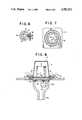
- the SMIF systemconsists of a semiconductor wafer cassette 6 for housing a predetermined number of semiconductor wafers 7, a SMIF pod 8 for enclosing the semiconductor wafer cassette 6 airtightly and for transferring the semiconductor wafers 7 in the cassette 6 without exposing them to outside contamination, a wafer processing equipment 1 for processing the semiconductor wafers 7, and a pair of SMIF arms 4 and 4 provided on both sides of the processing equipment 1 for loading and unloading the cassette 6 to and from the processing equipment 1.
- the SMIF pod 8consists of a box-like pod body with an open bottom and a bottom plate 10 for closing the bottom of the pod body 9.
- the bottom plate 10is detachably attached to the pod body 9 by latches (not shown) provided on the pod body 9 and is arranged to support the cassette 6 at a proper position when the cassette 6 is enclosed in the pod 8.
- the bottom plate 10 of the SMIF pod 8is fixed to the pod body 9 while the pod 8 is transported by a worker or a conveying apparatus.
- the wafer processing equipment 1consists of an equipment body 2 having a first port for the cassette 6, a transparent canopy 5 for covering an upper surface of the equipment body 2, and a clean air supply unit 3 mounted on the canopy 5.
- This clean air supply unit 3having a high-performance filter and a blower supplies the wafer processing equipment 1 with clean air.
- the cassette 6 enclosed in the SMIF pod 8is placed on the upper face of one of the SMIF arms 4.
- the bottom plate 10 of the pod 8is detached from the pod body 9, and then the bottom plate 10 and the cassette 6 supported on it are loaded into the SMIF arm 4. Thereafter, only the cassette 6 is transferred into the processing equipment 1, set in the first port, and then the wafers 7 in it are withdrawn to be processed.
- the wafers 7are housed in another cassette (not shown) and are loaded in the other SMIF arm 4.
- the cassetteis brought into another SMIF pod (not shown) which has been placed on the upper face of the other SMIF arm 4 without being exposed to outside contamination.
- the pod 8 which has just received the cassetteis transported, for example, by a worker to another processing equipment (not shown) of the next fabrication process and then placed on an SMIF arm of this equipment. Thereafter, the wafers 7 are processed in the equipment in the same manner as described above.
- the wafersare not exposed to outside contamination but kept in clean air while being transported by workers and being transferred between the pod 8 and the equipment 1 as well as while being processed in the processing equipment. Therefore, a high product yield is maintained by using this SMIF system even when cleanliness (based on U.S. Federal Standard No. 209b) of a clean room in which the system is installed is about class 1,000 to 100,000.
- cleanlinessbased on U.S. Federal Standard No. 209b
- a non-laminar flow air current systemwhich keeps its environment at cleanliness of class 1,000 to 100,000 is possibly employed in the clean room in place of a laminar flow air current system which keeps its environment at ultra high cleanliness of class 10 to 100. That is, associated facilities of the clean room become simple, and costs for its construction, facilities, and maintenances can be greatly reduced.
- the SMIF systemit is not necessary, if the SMIF system is used, to limit the behaviour of workers who works in the clean room as strictly as it is limited in a clean room with ultra high cleanliness of class 10 to 100.
- the workersare allowed to work as if they are in an ordinary room on condition that they will wear simple clean room clothes. They are able to work more comfortably in this clean room using the SMIF system than in one not using it.
- the present inventionprovides a semiconductor processing system which includes: a first semiconductor wafer cassette for housing semiconductor wafers; a first transfer pod for enclosing the first cassette airtightly, the first pod having a box-like pod body with an open bottom and a bottom plate detachably attached to the pod body for closing the bottom of the pod body; a wafer processing equipment having a first port for loading the cassette and a canopy covering the first port, the processing equipment processing the wafer in the first cassette when the cassette is loaded in the first port; and a first mechanism for transferring the first cassette between the first port of the processing equipment and the first pod without exposing the cassette and the wafers therein to outside contamination.
- the first transferring mechanismincludes: a second port, provided on the canopy of the processing equipment at the position directly above the first port, for placing the first pod on the second port, the second port including a port assembly for attaching and detaching the bottom plate of the first pod to and from the pod body when the first pod is placed on the second port; and a first lift mechanism, arranged mainly between the first and second ports, for conveying the bottom plate of the first pod between the first and second ports when the bottom plate of the pod is detached from the pod body.
- the systemhas a second mechanism for transferring another cassette into and out of the processing equipment.
- the processing equipmentmay have a third port for loading the cassette, which is covered with the canopy, and a mechanism for processing the wafers in the first cassette in the first port and transferring the wafers into the cassette in the third port when the cassette with the wafers and the cassette being empty are loaded in the first and third ports respectively.
- the second transferring mechanismmay have a fourth port, provided on the canopy of the processing equipment at the position directly above the third port, for placing the second pod thereon, and a second lift mechanism, arranged mainly between the third and fourth ports, for conveying the cassette between the third and fourth ports. In this case, the cassette housing the wafers which have been processed by the processing mechanism is transferred from the third port to the fourth port and enclosed in another pod.
- the second porthas a cassette opening formed in the canopy of the processing equipment.
- the first lift mechanismhas a door plate for opening and closing the cassette opening of the second port.
- the door platesupports the bottom plate of the pod when the pod is placed on the second port.
- the lift mechanismmay also have a drive unit for driving the door plate upwards and downwards.
- the first transferring mechanismmay have a mechanism for turning the bottom plate of the transfer pod about an axis perpendicular thereto so that the horizontal orientation of the bottom plate is controlled.
- the rotating mechanismit is not necessary to make the orientation of the cassette coincide with the predetermined orientation in the processing equipment before the pod is placed on the second port, since the orientation of the cassette can be changed even after the pod is placed on the second port.
- the system with this arrangementaccelerates the total system automation such as the system of the above construction with automatic conveyers arranged between different processing equipments.
- the processing equipmentmay have a clean air supply unit for maintaining the interior of the processing equipment at ultra high cleanliness.
- FIG. 1is a schematic perspective view of a conventional semiconductor processing system
- FIG. 2is a sectional view of an SMIF pod in FIG. 1;
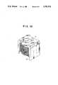
- FIG. 3is a schematic front view of a semiconductor processing system according to the present invention.
- FIG. 4is a schematic plan view of the semiconductor processing system in FIG. 3;
- FIG. 5is an enlarged sectional view of a second port, a first port, and a lift mechanism in FIG. 3;
- FIG. 6is a view taken along the line VI--VI in FIG. 5;
- FIG. 7is a view taken along the line VII--VII in FIG. 5;
- FIG. 8is a sectional view of the second port in FIG. 3 showing a transfer pod placed thereon;
- FIG. 9is a sectional view of the second port and the first port in FIG. 5 showing a cassette loaded in the first port;
- FIG. 10is an enlarged perspective view of the cassette in FIG. 3 showing wafers housed therein.
- FIGS. 3 to 10the same parts as those in FIGS. 1 and 2 are designated by the same reference numerals, and a description thereof will be omitted.
- FIGS. 3 and 4show a semiconductor processing system according to the present invention.
- a wafer processing equipment 20has upwardly open first and third ports 22 and 24 for loading and unloading the semiconductor wafer cassette 6 and a canopy which covers the first and third ports, 22 and 24.
- the canopy 26is provided at its portions directly above the first and third ports 22 and 24 with second and fourth ports 28 and 30 on which the transfer pods (SMIF pods) 8 are placed.
- SMIF podstransfer pods
- a pod 8is placed on each of the second and fourth ports 28 and 30.
- a pod 8 on the second port 28contains a cassette 6 having the wafers 7 therein and the other pod 8 on the fourth port 30 encloses an empty cassette 6.
- the processing equipment 20has an processing assembly in it which processes the wafers 7 in the cassette 6 in the first port 22 and transfers the wafers 7 into the cassette 6 in the third port 24 when the cassette 6 with the wafers 7 is set in the first port 22 and the empty cassette 6 is set in the third port 24. Therefore, the first port 22 is a loading port, and the third port 24 is a unloading port.
- the clean air supply unit 3which is mounted on the canopy 26 consists of a blower and a high-performance filter such as a ULPA (Ultra Low Penetration Air) filter and a HEPA (High Efficiency Particulate Air) filter.
- the clean air supply unit 3supplies the processing equipment 20 with clean air to maintain the interior of the equipment at ultra high cleanliness.
- the unit 3also sets the interior of the processing equipment 20 at a positive pressure higher than atmospheric pressure so that dust generated inside the equipment 20 is immediately exhausted outside the equipment 20 through ventilating slits 32 formed in the side wall of the canopy 26 and air exhaust openings open at the bottom of the processing equipment 20.
- each of the second and fourth ports 28 and 30has a cassette opening 34 formed in the canopy 26 and a port assembly 36 provided around the opening 34.
- the opening 34has its inner diameter slightly larger than the diameter of the bottom plate 10 of the pod 8 and smaller than the outer diameter of the pod body 9.
- the port assembly 36includes guides 38 disposed along the periphery of the opening 34, engaging sliders 40 slidably provided on the guides 38, a drive source such as a motor (not shown) for horizontally sliding the sliders 40 toward the center of the opening 34 and away therefrom, and a sensor such as an optical sensor (not shown) for detecting whether a pod 8 is in the corresponding port 28 or 30.
- the sensorgenerates a signal for turning on the drive source of the port assembly 36 when detecting the pod 8 in the port.
- a first lift mechanism 42is provided between the first and second ports 22 and 28.
- a second lift mechanism 44is provided between the third and fourth ports 24 and 30.
- Each of the lift mechanisms 42 and 44has a door plate 46 for opening and closing the cassette opening 34.
- This door plate 46supports the bottom plate 10 of the pod 8 when the pod 8 is placed on the corresponding first or third port 28 or 30.
- the plate 46is supported by a hollow drive shaft 52.
- the drive shaft 52has an upper end portion 52a having a larger diameter than the other portion thereof, and is connected the upper end portion 52a via a magnetically sealed thrust bearing 48 to the lower surface of the door plate 46 so that the door plate 46 can rotate in a horizontal plane relative to the shaft 52.
- the lower end portion 52b of the shaft 52is concentrically engaged with a vertrical guide tube 50, which is arranged under the corresponding port 22 or 24, so that the shaft 52 is vertically slidable relative to the guide tube 50.
- the drive shaft 52has splines 51 on the outer face thereof, which are received in keyways 55 formed in the inner face of the guide tube 50, thereby prevented from rotating.
- Engaging teeth 53are formed on and along the drive shaft 52 so that a lower part of the drive shaft 52 serves as a rack.
- a pinion 54is meshed with the engaging teeth 53 through a slot 58, which is formed through the wall of guide tube 50, and is connected to a stepping motor 56 secured to a casing of the equipment 20. When the stepping motor 56 is on to rotate the pinion 54, the drive shaft 52 is reciprocated vertically to drive the door plate 46 upward and downward.
- an internal gear 62is fixed to the lower surface of the door plate 46, and a small gear 64 is meshed with the internal gear 62.
- the gear 64is directly connected to an orientation control motor 66 which is secured to the inner face of the upper end portion 52a of the shaft 52. That is, by turning the control motor 66 on and off with a proper controlling unit, the door plate 46 is turned in a horizontal plane with respect to the drive shaft 52 so that the orientation of the bottom plate 10 of the pod 8 placed on the door plate 46, i.e., the horizontal orientation of the cassette 6 on the bottom plate 10 is suitably controlled.
- the guide tube 50is in fluid communication with a vacuum pump (not shown) so that dust generated inside the upper end portion 52a of the shaft 52 is conveyed outside the equipment 20 through the guide tube 50.
- a plurality of projections 68are provided on the upper surface of the door plate 46. These projections 68 engage with the bottom plate 10 of the pod 8 so as to prevent the bottom plate 10 from slipping circumferentially during the turn of the door plate 46.
- the pod body 9 of the pod 8has an outer flange 70 at its lower end.
- a plurality of latches 72are pivotally connected to the outer flange 70 to be pivoted about pins 74.
- An upper end portion of each latch 72projects above the outer flange 70, and its lower end portion is bent like a hook.
- Each latch 72is biased at its lower end portion toward the center of the opening 34 by a spring (not shown) thereby kept in a position shown in FIG. 6 and engaging with the lower surface of the bottom plate 10 of the pod 8.
- the bottom plate 10is detached from the pod body 9 by disengaging the latches 72 from the lower surface of the bottom plate 10.
- the bottom plate 10 of the pod 8has recesses 76 on its lower surface for engaging with the projections 68 of the door plate 46.
- the door plate 46 of the corresponding lift mechanism 42 or 44is in direct contact with that portion of the canopy 26 surrounding the opening 34, and thus the opening 34 is closed airtightly.
- the sensor of the port assembly 36detects the placement of the pod 8 and operates the drive source of the port assembly 36. Then, the slider 40 is translated toward the center of the opening 34 (in the direction indicated by the arrow A) and is engaged with the outer flange 70 of the pod body 9 to fix the pod body 9 to the canopy 26 of the equipment 20.
- the lift mechanism 42When the lift mechanism 42 is operated to drive the door plate 46 downward, the bottom plate 10 of the pod 8 is conveyed downward together with the door plate 46. Therefore, the cassette 6 on the bottom plate 10 is transferred into the loading port 22, as shown in FIG. 9. During this downward movement, the door plate 46 is turned properly to make the horizontal orientation of the cassette coincide with the predetermined orientation of the cassette in the processing equipment 20.
- the wafers 7 in the cassette 6 which is loaded in the first port 22are sequentially withdrawn one by one from the bottom of the cassette 6 and transferred to a processing assembly in the equipment 20.
- the door plate 46is driven downward in units of predetermined pitches. Therefore, the wafers 7 to be removed next is always kept at the position where comes close enough to oppose the vacuum chuck 78 without vertical movement of the vacuum chuck 78.
- the cassette 6is loaded in the first port 22 together with the bottom plate 10 of the pod 8. Therefore, as shown in FIG. 10, the cassette 6 is provided at its bottom with legs 80 so that a room into which the vacuum chuck 78 enters is assured in the cassette 6.
- an empty cassette 6is set in the unloading port 24 by using the fourth port 30 and the lift mechanism 44. Then, the wafers 7 which have been processed in the equipment 20 are transferred into the cassette 6 at the unloading port 24. In this process, the wafers 7 fill the cassette 6 sequentially from the uppermost step of the cassette 6 to the lowermost step. This order of filling process is opposite to that of wafer withdrawing process. Therefore, the door plate 46 is driven this time upward in units of predetermined pitches, whenever a wafer 7 is housed in the cassette 6.
- the cassettes 6 at the loading and unloading ports 22 and 24are conveyed upward to the second and fourth ports 28 and 30 respectively by the lift mechanisms and are enclosed in the respective pod bodies 9 fixed to the second and fourth ports 28 and 30.
- the sliders 40 of the port assembly 36are slid in the direction opposite to that of the arrow A, the pod body 9 of each pod 8 is detached from the canopy 26 and the lower end portions of the latches 72 are returned to the positions shown in FIG. 8 by the bias force of the springs. Therefore, the bottom plate 10 of each pod 8 is fixed to its pod body 9.
- each pod 8is ready to be transported. Accordingly, the pod 8 on the second port 28 is removed from the equipment 20 and the pod 8 on the fourth port 30 is transported to another processing equipment (not shown) by a worker, a transferring equipment or the like for the next process.
- the cassetteis transferred between the pod and the processing equipment by the second and fourth ports 28 and 30 which are directly above the first and third ports 22 and 24 respectively and the lift mechanisms 42 and 44, it is not necessary to provide SMIF arms at the both side of the processing equipment. Accordingly, the installation area for the SMIF arms is effectively utilized as a free space in a clean room by slightly modifying conventional semiconductor processing systems, and the cost of the entire processing system is reduced.
- the guide tube 50may be connected to a vertical guide rail so as to move upwards and downwards.
- teethmay be formed on the outer face of the tube 50 in order to drive the tube with a stepping motor, and the pinion 54 may be meshed with the teeth 53 so as to be removable from it.
- the present inventionis not limited to this embodiment.
- clean air produced in a main air conditionermay be introduced via a duct into the processing equipment 20 instead of being supplied by the clean air supply unit 3.
- the lift mechanismmay be constituted of a ball screw assembly or an extendable component formed like a pantagraph in place of the rack drive shaft 52, the stepping motor 56, and the like.
Landscapes
- Engineering & Computer Science (AREA)
- Physics & Mathematics (AREA)
- Condensed Matter Physics & Semiconductors (AREA)
- General Physics & Mathematics (AREA)
- Manufacturing & Machinery (AREA)
- Computer Hardware Design (AREA)
- Microelectronics & Electronic Packaging (AREA)
- Power Engineering (AREA)
- Container, Conveyance, Adherence, Positioning, Of Wafer (AREA)
Abstract
Description
Claims (8)
Applications Claiming Priority (2)
| Application Number | Priority Date | Filing Date | Title |
|---|---|---|---|
| JP61-66761 | 1986-03-25 | ||
| JP61066761AJPS62222625A (en) | 1986-03-25 | 1986-03-25 | semiconductor manufacturing equipment |
Publications (1)
| Publication Number | Publication Date |
|---|---|
| US4781511Atrue US4781511A (en) | 1988-11-01 |
Family
ID=13325187
Family Applications (1)
| Application Number | Title | Priority Date | Filing Date |
|---|---|---|---|
| US06/932,182Expired - Fee RelatedUS4781511A (en) | 1986-03-25 | 1986-11-18 | Semiconductor processing system |
Country Status (6)
| Country | Link |
|---|---|
| US (1) | US4781511A (en) |
| EP (1) | EP0238751B1 (en) |
| JP (1) | JPS62222625A (en) |
| KR (1) | KR940002914B1 (en) |
| CA (1) | CA1267978A (en) |
| DE (1) | DE3687795T2 (en) |
Cited By (328)
| Publication number | Priority date | Publication date | Assignee | Title |
|---|---|---|---|---|
| US4895107A (en)* | 1987-07-06 | 1990-01-23 | Kabushiki Kaisha Toshiba | Photo chemical reaction apparatus |
| US4907526A (en)* | 1988-05-03 | 1990-03-13 | Leybold Aktiengesellschaft | Installation for charging and discharging substrates out of a vacuum tank |
| US4987673A (en)* | 1987-06-18 | 1991-01-29 | Mitsubishi Denki Kabushiki Kaisha | Apparatus for packaging semiconductor devices |
| US5033927A (en)* | 1989-03-17 | 1991-07-23 | Etudes Et Constructions Mechaniques | Device for carrying out sequential thermal treatments under a vacuum |
| US5058491A (en)* | 1990-08-27 | 1991-10-22 | Taiwan Semiconductor Manufacturing Company, Ltd. | Building and method for manufacture of integrated circuits |
| US5069269A (en)* | 1989-01-23 | 1991-12-03 | Leybold Aktiengesellschaft | Lifting and turning unit for a melting and/or casting plant |
| US5092728A (en)* | 1987-10-15 | 1992-03-03 | Epsilon Technology, Inc. | Substrate loading apparatus for a CVD process |
| US5092557A (en)* | 1990-03-05 | 1992-03-03 | Tet Techno Investment Trust Settlement | Apparatus for holding and positioning a substrate cassette |
| US5100287A (en)* | 1989-04-27 | 1992-03-31 | Micron Technology, Inc. | Method of transferring wafers using vacuum |
| WO1992007759A1 (en)* | 1990-11-01 | 1992-05-14 | Asyst Technologies, Inc. | Method and apparatus for transferring articles between two controlled environments |
| US5145303A (en)* | 1991-02-28 | 1992-09-08 | Mcnc | Method and apparatus for reducing particulate contamination in processing chambers |
| US5156521A (en)* | 1987-10-15 | 1992-10-20 | Epsilon Technology, Inc. | Method for loading a substrate into a GVD apparatus |
| US5176493A (en)* | 1989-02-24 | 1993-01-05 | North American Philips Corporation | High speed wafer handling method |
| US5261776A (en)* | 1989-04-27 | 1993-11-16 | Micron Technology, Inc. | Vacuum operated wafer transfer apparatus |
| US5339952A (en)* | 1992-06-19 | 1994-08-23 | International Business Machines Corporation | Transfer container for transferring flimsy circuit panels under clean room conditions |
| US5350336A (en)* | 1993-04-23 | 1994-09-27 | Industrial Technology Research Institute | Building and method for manufacture of integrated semiconductor circuit devices |
| US5364225A (en)* | 1992-06-19 | 1994-11-15 | Ibm | Method of printed circuit panel manufacture |
| US5395198A (en)* | 1992-06-19 | 1995-03-07 | International Business Machines Corporation | Vacuum loading chuck and fixture for flexible printed circuit panels |
| US5404894A (en)* | 1992-05-20 | 1995-04-11 | Tokyo Electron Kabushiki Kaisha | Conveyor apparatus |
| US5451131A (en)* | 1992-06-19 | 1995-09-19 | International Business Machines Corporation | Dockable interface airlock between process enclosure and interprocess transfer container |
| US5494524A (en)* | 1992-12-17 | 1996-02-27 | Toshiba Ceramics Co., Ltd. | Vertical heat treatment device for semiconductor |
| US5537311A (en)* | 1993-01-28 | 1996-07-16 | Applied Materials, Inc. | Apparatus for aligning substrates for loading and unloading using a robot mechanism |
| US5538390A (en)* | 1993-10-29 | 1996-07-23 | Applied Materials, Inc. | Enclosure for load lock interface |
| WO1997003222A1 (en)* | 1995-07-10 | 1997-01-30 | Asyst Technologies, Inc. | Cassette support and rotation assembly |
| US5628604A (en)* | 1994-05-17 | 1997-05-13 | Shinko Electric Co., Ltd. | Conveying system |
| US5642978A (en)* | 1993-03-29 | 1997-07-01 | Jenoptik Gmbh | Device for handling disk-shaped objects in a handling plane of a local clean room |
| US5674039A (en)* | 1996-07-12 | 1997-10-07 | Fusion Systems Corporation | System for transferring articles between controlled environments |
| US5697749A (en)* | 1992-07-17 | 1997-12-16 | Tokyo Electron Kabushiki Kaisha | Wafer processing apparatus |
| US5700725A (en)* | 1995-06-26 | 1997-12-23 | Lucent Technologies Inc. | Apparatus and method for making integrated circuits |
| US5709519A (en)* | 1992-01-22 | 1998-01-20 | Tokyo Ohka Kogyo Co., Ltd. | Plasma processing apparatus |
| US5713711A (en)* | 1995-01-17 | 1998-02-03 | Bye/Oasis | Multiple interface door for wafer storage and handling container |
| US5769184A (en)* | 1996-09-27 | 1998-06-23 | Brooks Automation, Inc. | Coaxial drive elevator |
| US5807062A (en)* | 1995-12-28 | 1998-09-15 | Jenoptik Aktiengesellschaft | Arrangement for handling wafer-shaped objects |
| US5947675A (en)* | 1996-11-13 | 1999-09-07 | Tokyo Electron Limited | Cassette transfer mechanism |
| US5951776A (en)* | 1996-10-25 | 1999-09-14 | Applied Materials, Inc. | Self aligning lift mechanism |
| US5957648A (en)* | 1996-12-11 | 1999-09-28 | Applied Materials, Inc. | Factory automation apparatus and method for handling, moving and storing semiconductor wafer carriers |
| US5964561A (en)* | 1996-12-11 | 1999-10-12 | Applied Materials, Inc. | Compact apparatus and method for storing and loading semiconductor wafer carriers |
| WO1999063581A1 (en)* | 1998-06-03 | 1999-12-09 | Tec-Sem Ag | Device and method for handling a container |
| US6168427B1 (en)* | 1999-10-05 | 2001-01-02 | Taiwan Semiconductor Manufacturing Co., Ltd | Apparatus for guiding the removal of a processing tube from a semiconductor furnace |
| US6549825B2 (en)* | 2000-09-14 | 2003-04-15 | Olympus Optical Co., Ltd. | Alignment apparatus |
| US6692209B1 (en)* | 1999-11-19 | 2004-02-17 | Litton Systems, Inc. | Method and system for manufacturing a photocathode |
| US6704998B1 (en)* | 1997-12-24 | 2004-03-16 | Asyst Technologies, Inc. | Port door removal and wafer handling robotic system |
| EP1086030A4 (en)* | 1998-05-05 | 2004-10-13 | Asyst Technologies | Smif pod including independently supported wafer cassette |
| US6843541B1 (en)* | 2002-06-06 | 2005-01-18 | The United States Of America As Represented By The United States Department Of Energy | Glove box for water pit applications |
| EP1345256A3 (en)* | 2002-03-15 | 2005-07-06 | Asm International N.V. | Method and apparatus for batch processing of wafers in a furnace |
| US20050201854A1 (en)* | 2002-05-10 | 2005-09-15 | Toshirou Kisakibaru | Semiconductor manufacturing apparatus of minienvironment system |
| US7092779B1 (en)* | 1997-06-19 | 2006-08-15 | Conboy Michael R | Automated material handling system for a manufacturing facility divided into separate fabrication areas |
| US20070243048A1 (en)* | 1996-12-11 | 2007-10-18 | Applied Materials, Inc. | Compact apparatus and method for storing and loading semiconductor wafer carriers |
| US7416998B2 (en) | 2002-12-03 | 2008-08-26 | Kondoh Industries, Ltd. | Air-curtain forming apparatus for wafer hermetic container in semiconductor-fabrication equipment of minienvironment system |
| US20170170356A1 (en)* | 2015-12-14 | 2017-06-15 | Solarcity Corporation | Load lock solar cell transfer system and methods |
| US10192765B2 (en)* | 2013-08-12 | 2019-01-29 | Applied Materials, Inc. | Substrate processing systems, apparatus, and methods with factory interface environmental controls |
| US10359743B2 (en) | 2014-11-25 | 2019-07-23 | Applied Materials, Inc. | Substrate processing systems, apparatus, and methods with substrate carrier and purge chamber environmental controls |
| US11001925B2 (en) | 2016-12-19 | 2021-05-11 | Asm Ip Holding B.V. | Substrate processing apparatus |
| US11004977B2 (en) | 2017-07-19 | 2021-05-11 | Asm Ip Holding B.V. | Method for depositing a group IV semiconductor and related semiconductor device structures |
| US11015245B2 (en) | 2014-03-19 | 2021-05-25 | Asm Ip Holding B.V. | Gas-phase reactor and system having exhaust plenum and components thereof |
| US11018002B2 (en) | 2017-07-19 | 2021-05-25 | Asm Ip Holding B.V. | Method for selectively depositing a Group IV semiconductor and related semiconductor device structures |
| US11022879B2 (en) | 2017-11-24 | 2021-06-01 | Asm Ip Holding B.V. | Method of forming an enhanced unexposed photoresist layer |
| US11031242B2 (en) | 2018-11-07 | 2021-06-08 | Asm Ip Holding B.V. | Methods for depositing a boron doped silicon germanium film |
| USD922229S1 (en) | 2019-06-05 | 2021-06-15 | Asm Ip Holding B.V. | Device for controlling a temperature of a gas supply unit |
| US11049751B2 (en) | 2018-09-14 | 2021-06-29 | Asm Ip Holding B.V. | Cassette supply system to store and handle cassettes and processing apparatus equipped therewith |
| US11056344B2 (en) | 2017-08-30 | 2021-07-06 | Asm Ip Holding B.V. | Layer forming method |
| US11053591B2 (en) | 2018-08-06 | 2021-07-06 | Asm Ip Holding B.V. | Multi-port gas injection system and reactor system including same |
| US11069510B2 (en) | 2017-08-30 | 2021-07-20 | Asm Ip Holding B.V. | Substrate processing apparatus |
| US11081345B2 (en) | 2018-02-06 | 2021-08-03 | Asm Ip Holding B.V. | Method of post-deposition treatment for silicon oxide film |
| US11088002B2 (en) | 2018-03-29 | 2021-08-10 | Asm Ip Holding B.V. | Substrate rack and a substrate processing system and method |
| US11087997B2 (en) | 2018-10-31 | 2021-08-10 | Asm Ip Holding B.V. | Substrate processing apparatus for processing substrates |
| US11094546B2 (en) | 2017-10-05 | 2021-08-17 | Asm Ip Holding B.V. | Method for selectively depositing a metallic film on a substrate |
| US11094582B2 (en) | 2016-07-08 | 2021-08-17 | Asm Ip Holding B.V. | Selective deposition method to form air gaps |
| US11101370B2 (en) | 2016-05-02 | 2021-08-24 | Asm Ip Holding B.V. | Method of forming a germanium oxynitride film |
| US11107676B2 (en) | 2016-07-28 | 2021-08-31 | Asm Ip Holding B.V. | Method and apparatus for filling a gap |
| US11114294B2 (en) | 2019-03-08 | 2021-09-07 | Asm Ip Holding B.V. | Structure including SiOC layer and method of forming same |
| US11114283B2 (en) | 2018-03-16 | 2021-09-07 | Asm Ip Holding B.V. | Reactor, system including the reactor, and methods of manufacturing and using same |
| USD930782S1 (en) | 2019-08-22 | 2021-09-14 | Asm Ip Holding B.V. | Gas distributor |
| US11127617B2 (en) | 2017-11-27 | 2021-09-21 | Asm Ip Holding B.V. | Storage device for storing wafer cassettes for use with a batch furnace |
| US11127589B2 (en) | 2019-02-01 | 2021-09-21 | Asm Ip Holding B.V. | Method of topology-selective film formation of silicon oxide |
| USD931978S1 (en) | 2019-06-27 | 2021-09-28 | Asm Ip Holding B.V. | Showerhead vacuum transport |
| US11139191B2 (en) | 2017-08-09 | 2021-10-05 | Asm Ip Holding B.V. | Storage apparatus for storing cassettes for substrates and processing apparatus equipped therewith |
| US11139308B2 (en) | 2015-12-29 | 2021-10-05 | Asm Ip Holding B.V. | Atomic layer deposition of III-V compounds to form V-NAND devices |
| US11158513B2 (en) | 2018-12-13 | 2021-10-26 | Asm Ip Holding B.V. | Methods for forming a rhenium-containing film on a substrate by a cyclical deposition process and related semiconductor device structures |
| US11164955B2 (en) | 2017-07-18 | 2021-11-02 | Asm Ip Holding B.V. | Methods for forming a semiconductor device structure and related semiconductor device structures |
| USD935572S1 (en) | 2019-05-24 | 2021-11-09 | Asm Ip Holding B.V. | Gas channel plate |
| US11171025B2 (en) | 2019-01-22 | 2021-11-09 | Asm Ip Holding B.V. | Substrate processing device |
| US11168395B2 (en) | 2018-06-29 | 2021-11-09 | Asm Ip Holding B.V. | Temperature-controlled flange and reactor system including same |
| US11205585B2 (en) | 2016-07-28 | 2021-12-21 | Asm Ip Holding B.V. | Substrate processing apparatus and method of operating the same |
| US11217444B2 (en) | 2018-11-30 | 2022-01-04 | Asm Ip Holding B.V. | Method for forming an ultraviolet radiation responsive metal oxide-containing film |
| USD940837S1 (en) | 2019-08-22 | 2022-01-11 | Asm Ip Holding B.V. | Electrode |
| US11222772B2 (en) | 2016-12-14 | 2022-01-11 | Asm Ip Holding B.V. | Substrate processing apparatus |
| US11227782B2 (en) | 2019-07-31 | 2022-01-18 | Asm Ip Holding B.V. | Vertical batch furnace assembly |
| US11227789B2 (en) | 2019-02-20 | 2022-01-18 | Asm Ip Holding B.V. | Method and apparatus for filling a recess formed within a substrate surface |
| US11230766B2 (en) | 2018-03-29 | 2022-01-25 | Asm Ip Holding B.V. | Substrate processing apparatus and method |
| US11233133B2 (en) | 2015-10-21 | 2022-01-25 | Asm Ip Holding B.V. | NbMC layers |
| US11232963B2 (en) | 2018-10-03 | 2022-01-25 | Asm Ip Holding B.V. | Substrate processing apparatus and method |
| US11244825B2 (en) | 2018-11-16 | 2022-02-08 | Asm Ip Holding B.V. | Methods for depositing a transition metal chalcogenide film on a substrate by a cyclical deposition process |
| US11242598B2 (en) | 2015-06-26 | 2022-02-08 | Asm Ip Holding B.V. | Structures including metal carbide material, devices including the structures, and methods of forming same |
| US11251040B2 (en) | 2019-02-20 | 2022-02-15 | Asm Ip Holding B.V. | Cyclical deposition method including treatment step and apparatus for same |
| US11251068B2 (en) | 2018-10-19 | 2022-02-15 | Asm Ip Holding B.V. | Substrate processing apparatus and substrate processing method |
| US11251035B2 (en) | 2016-12-22 | 2022-02-15 | Asm Ip Holding B.V. | Method of forming a structure on a substrate |
| USD944946S1 (en) | 2019-06-14 | 2022-03-01 | Asm Ip Holding B.V. | Shower plate |
| US11270899B2 (en) | 2018-06-04 | 2022-03-08 | Asm Ip Holding B.V. | Wafer handling chamber with moisture reduction |
| US11274369B2 (en) | 2018-09-11 | 2022-03-15 | Asm Ip Holding B.V. | Thin film deposition method |
| US11282698B2 (en) | 2019-07-19 | 2022-03-22 | Asm Ip Holding B.V. | Method of forming topology-controlled amorphous carbon polymer film |
| US11289326B2 (en) | 2019-05-07 | 2022-03-29 | Asm Ip Holding B.V. | Method for reforming amorphous carbon polymer film |
| US11286562B2 (en) | 2018-06-08 | 2022-03-29 | Asm Ip Holding B.V. | Gas-phase chemical reactor and method of using same |
| US11286558B2 (en) | 2019-08-23 | 2022-03-29 | Asm Ip Holding B.V. | Methods for depositing a molybdenum nitride film on a surface of a substrate by a cyclical deposition process and related semiconductor device structures including a molybdenum nitride film |
| US11295980B2 (en) | 2017-08-30 | 2022-04-05 | Asm Ip Holding B.V. | Methods for depositing a molybdenum metal film over a dielectric surface of a substrate by a cyclical deposition process and related semiconductor device structures |
| US11296189B2 (en) | 2018-06-21 | 2022-04-05 | Asm Ip Holding B.V. | Method for depositing a phosphorus doped silicon arsenide film and related semiconductor device structures |
| USD947913S1 (en) | 2019-05-17 | 2022-04-05 | Asm Ip Holding B.V. | Susceptor shaft |
| USD948463S1 (en) | 2018-10-24 | 2022-04-12 | Asm Ip Holding B.V. | Susceptor for semiconductor substrate supporting apparatus |
| US11306395B2 (en) | 2017-06-28 | 2022-04-19 | Asm Ip Holding B.V. | Methods for depositing a transition metal nitride film on a substrate by atomic layer deposition and related deposition apparatus |
| USD949319S1 (en) | 2019-08-22 | 2022-04-19 | Asm Ip Holding B.V. | Exhaust duct |
| US11315794B2 (en) | 2019-10-21 | 2022-04-26 | Asm Ip Holding B.V. | Apparatus and methods for selectively etching films |
| US11339476B2 (en) | 2019-10-08 | 2022-05-24 | Asm Ip Holding B.V. | Substrate processing device having connection plates, substrate processing method |
| US11342216B2 (en) | 2019-02-20 | 2022-05-24 | Asm Ip Holding B.V. | Cyclical deposition method and apparatus for filling a recess formed within a substrate surface |
| US11345999B2 (en) | 2019-06-06 | 2022-05-31 | Asm Ip Holding B.V. | Method of using a gas-phase reactor system including analyzing exhausted gas |
| US11355338B2 (en) | 2019-05-10 | 2022-06-07 | Asm Ip Holding B.V. | Method of depositing material onto a surface and structure formed according to the method |
| US11361990B2 (en) | 2018-05-28 | 2022-06-14 | Asm Ip Holding B.V. | Substrate processing method and device manufactured by using the same |
| US11374112B2 (en) | 2017-07-19 | 2022-06-28 | Asm Ip Holding B.V. | Method for depositing a group IV semiconductor and related semiconductor device structures |
| US11378337B2 (en) | 2019-03-28 | 2022-07-05 | Asm Ip Holding B.V. | Door opener and substrate processing apparatus provided therewith |
| US11387106B2 (en) | 2018-02-14 | 2022-07-12 | Asm Ip Holding B.V. | Method for depositing a ruthenium-containing film on a substrate by a cyclical deposition process |
| US11387120B2 (en) | 2017-09-28 | 2022-07-12 | Asm Ip Holding B.V. | Chemical dispensing apparatus and methods for dispensing a chemical to a reaction chamber |
| US11393690B2 (en) | 2018-01-19 | 2022-07-19 | Asm Ip Holding B.V. | Deposition method |
| US11390950B2 (en) | 2017-01-10 | 2022-07-19 | Asm Ip Holding B.V. | Reactor system and method to reduce residue buildup during a film deposition process |
| US11390946B2 (en) | 2019-01-17 | 2022-07-19 | Asm Ip Holding B.V. | Methods of forming a transition metal containing film on a substrate by a cyclical deposition process |
| US11390945B2 (en) | 2019-07-03 | 2022-07-19 | Asm Ip Holding B.V. | Temperature control assembly for substrate processing apparatus and method of using same |
| US11398382B2 (en) | 2018-03-27 | 2022-07-26 | Asm Ip Holding B.V. | Method of forming an electrode on a substrate and a semiconductor device structure including an electrode |
| US11396702B2 (en) | 2016-11-15 | 2022-07-26 | Asm Ip Holding B.V. | Gas supply unit and substrate processing apparatus including the gas supply unit |
| US11401605B2 (en) | 2019-11-26 | 2022-08-02 | Asm Ip Holding B.V. | Substrate processing apparatus |
| US11410851B2 (en) | 2017-02-15 | 2022-08-09 | Asm Ip Holding B.V. | Methods for forming a metallic film on a substrate by cyclical deposition and related semiconductor device structures |
| US11411088B2 (en) | 2018-11-16 | 2022-08-09 | Asm Ip Holding B.V. | Methods for forming a metal silicate film on a substrate in a reaction chamber and related semiconductor device structures |
| US11414760B2 (en) | 2018-10-08 | 2022-08-16 | Asm Ip Holding B.V. | Substrate support unit, thin film deposition apparatus including the same, and substrate processing apparatus including the same |
| US11417545B2 (en) | 2017-08-08 | 2022-08-16 | Asm Ip Holding B.V. | Radiation shield |
| US11424119B2 (en) | 2019-03-08 | 2022-08-23 | Asm Ip Holding B.V. | Method for selective deposition of silicon nitride layer and structure including selectively-deposited silicon nitride layer |
| US11430640B2 (en) | 2019-07-30 | 2022-08-30 | Asm Ip Holding B.V. | Substrate processing apparatus |
| US11430674B2 (en) | 2018-08-22 | 2022-08-30 | Asm Ip Holding B.V. | Sensor array, apparatus for dispensing a vapor phase reactant to a reaction chamber and related methods |
| US11437241B2 (en) | 2020-04-08 | 2022-09-06 | Asm Ip Holding B.V. | Apparatus and methods for selectively etching silicon oxide films |
| US11443926B2 (en) | 2019-07-30 | 2022-09-13 | Asm Ip Holding B.V. | Substrate processing apparatus |
| US11447864B2 (en) | 2019-04-19 | 2022-09-20 | Asm Ip Holding B.V. | Layer forming method and apparatus |
| US11447861B2 (en) | 2016-12-15 | 2022-09-20 | Asm Ip Holding B.V. | Sequential infiltration synthesis apparatus and a method of forming a patterned structure |
| US11453943B2 (en) | 2016-05-25 | 2022-09-27 | Asm Ip Holding B.V. | Method for forming carbon-containing silicon/metal oxide or nitride film by ALD using silicon precursor and hydrocarbon precursor |
| USD965044S1 (en) | 2019-08-19 | 2022-09-27 | Asm Ip Holding B.V. | Susceptor shaft |
| USD965524S1 (en) | 2019-08-19 | 2022-10-04 | Asm Ip Holding B.V. | Susceptor support |
| US11469098B2 (en) | 2018-05-08 | 2022-10-11 | Asm Ip Holding B.V. | Methods for depositing an oxide film on a substrate by a cyclical deposition process and related device structures |
| US11476109B2 (en) | 2019-06-11 | 2022-10-18 | Asm Ip Holding B.V. | Method of forming an electronic structure using reforming gas, system for performing the method, and structure formed using the method |
| US11473195B2 (en) | 2018-03-01 | 2022-10-18 | Asm Ip Holding B.V. | Semiconductor processing apparatus and a method for processing a substrate |
| US11482533B2 (en) | 2019-02-20 | 2022-10-25 | Asm Ip Holding B.V. | Apparatus and methods for plug fill deposition in 3-D NAND applications |
| US11482418B2 (en) | 2018-02-20 | 2022-10-25 | Asm Ip Holding B.V. | Substrate processing method and apparatus |
| US11482412B2 (en) | 2018-01-19 | 2022-10-25 | Asm Ip Holding B.V. | Method for depositing a gap-fill layer by plasma-assisted deposition |
| US11488819B2 (en) | 2018-12-04 | 2022-11-01 | Asm Ip Holding B.V. | Method of cleaning substrate processing apparatus |
| US11488854B2 (en) | 2020-03-11 | 2022-11-01 | Asm Ip Holding B.V. | Substrate handling device with adjustable joints |
| EP3918106A4 (en)* | 2019-02-19 | 2022-11-02 | Veeco Instruments Inc. | AUTOMATED THIN FILM DEPOSITION SYSTEMS WITH VOLUME MANUFACTURE AND METHODS OF USE THEREOF |
| US11495459B2 (en) | 2019-09-04 | 2022-11-08 | Asm Ip Holding B.V. | Methods for selective deposition using a sacrificial capping layer |
| US11492703B2 (en) | 2018-06-27 | 2022-11-08 | Asm Ip Holding B.V. | Cyclic deposition methods for forming metal-containing material and films and structures including the metal-containing material |
| US11499226B2 (en) | 2018-11-02 | 2022-11-15 | Asm Ip Holding B.V. | Substrate supporting unit and a substrate processing device including the same |
| US11501973B2 (en) | 2018-01-16 | 2022-11-15 | Asm Ip Holding B.V. | Method for depositing a material film on a substrate within a reaction chamber by a cyclical deposition process and related device structures |
| US11501956B2 (en) | 2012-10-12 | 2022-11-15 | Asm Ip Holding B.V. | Semiconductor reaction chamber showerhead |
| US11501968B2 (en) | 2019-11-15 | 2022-11-15 | Asm Ip Holding B.V. | Method for providing a semiconductor device with silicon filled gaps |
| US11499222B2 (en) | 2018-06-27 | 2022-11-15 | Asm Ip Holding B.V. | Cyclic deposition methods for forming metal-containing material and films and structures including the metal-containing material |
| CN115360119A (en)* | 2022-07-27 | 2022-11-18 | 徐州市沂芯微电子有限公司 | Automatic encapsulation equipment for semiconductor chip |
| US11515188B2 (en) | 2019-05-16 | 2022-11-29 | Asm Ip Holding B.V. | Wafer boat handling device, vertical batch furnace and method |
| US11515187B2 (en) | 2020-05-01 | 2022-11-29 | Asm Ip Holding B.V. | Fast FOUP swapping with a FOUP handler |
| US11521851B2 (en) | 2020-02-03 | 2022-12-06 | Asm Ip Holding B.V. | Method of forming structures including a vanadium or indium layer |
| US11527403B2 (en) | 2019-12-19 | 2022-12-13 | Asm Ip Holding B.V. | Methods for filling a gap feature on a substrate surface and related semiconductor structures |
| US11527400B2 (en) | 2019-08-23 | 2022-12-13 | Asm Ip Holding B.V. | Method for depositing silicon oxide film having improved quality by peald using bis(diethylamino)silane |
| US11530876B2 (en) | 2020-04-24 | 2022-12-20 | Asm Ip Holding B.V. | Vertical batch furnace assembly comprising a cooling gas supply |
| US11530483B2 (en) | 2018-06-21 | 2022-12-20 | Asm Ip Holding B.V. | Substrate processing system |
| US11532757B2 (en) | 2016-10-27 | 2022-12-20 | Asm Ip Holding B.V. | Deposition of charge trapping layers |
| US11551912B2 (en) | 2020-01-20 | 2023-01-10 | Asm Ip Holding B.V. | Method of forming thin film and method of modifying surface of thin film |
| US11551925B2 (en) | 2019-04-01 | 2023-01-10 | Asm Ip Holding B.V. | Method for manufacturing a semiconductor device |
| USD975665S1 (en) | 2019-05-17 | 2023-01-17 | Asm Ip Holding B.V. | Susceptor shaft |
| US11557474B2 (en) | 2019-07-29 | 2023-01-17 | Asm Ip Holding B.V. | Methods for selective deposition utilizing n-type dopants and/or alternative dopants to achieve high dopant incorporation |
| US11562901B2 (en) | 2019-09-25 | 2023-01-24 | Asm Ip Holding B.V. | Substrate processing method |
| US11572620B2 (en) | 2018-11-06 | 2023-02-07 | Asm Ip Holding B.V. | Methods for selectively depositing an amorphous silicon film on a substrate |
| US11581186B2 (en) | 2016-12-15 | 2023-02-14 | Asm Ip Holding B.V. | Sequential infiltration synthesis apparatus |
| US11587814B2 (en) | 2019-07-31 | 2023-02-21 | Asm Ip Holding B.V. | Vertical batch furnace assembly |
| US11587821B2 (en) | 2017-08-08 | 2023-02-21 | Asm Ip Holding B.V. | Substrate lift mechanism and reactor including same |
| US11587815B2 (en) | 2019-07-31 | 2023-02-21 | Asm Ip Holding B.V. | Vertical batch furnace assembly |
| USD979506S1 (en) | 2019-08-22 | 2023-02-28 | Asm Ip Holding B.V. | Insulator |
| US11594450B2 (en) | 2019-08-22 | 2023-02-28 | Asm Ip Holding B.V. | Method for forming a structure with a hole |
| US11594600B2 (en) | 2019-11-05 | 2023-02-28 | Asm Ip Holding B.V. | Structures with doped semiconductor layers and methods and systems for forming same |
| USD980813S1 (en) | 2021-05-11 | 2023-03-14 | Asm Ip Holding B.V. | Gas flow control plate for substrate processing apparatus |
| USD980814S1 (en) | 2021-05-11 | 2023-03-14 | Asm Ip Holding B.V. | Gas distributor for substrate processing apparatus |
| US11605528B2 (en) | 2019-07-09 | 2023-03-14 | Asm Ip Holding B.V. | Plasma device using coaxial waveguide, and substrate treatment method |
| US11610775B2 (en) | 2016-07-28 | 2023-03-21 | Asm Ip Holding B.V. | Method and apparatus for filling a gap |
| US11610774B2 (en) | 2019-10-02 | 2023-03-21 | Asm Ip Holding B.V. | Methods for forming a topographically selective silicon oxide film by a cyclical plasma-enhanced deposition process |
| US11615970B2 (en) | 2019-07-17 | 2023-03-28 | Asm Ip Holding B.V. | Radical assist ignition plasma system and method |
| USD981973S1 (en) | 2021-05-11 | 2023-03-28 | Asm Ip Holding B.V. | Reactor wall for substrate processing apparatus |
| US11626308B2 (en) | 2020-05-13 | 2023-04-11 | Asm Ip Holding B.V. | Laser alignment fixture for a reactor system |
| US11626316B2 (en) | 2019-11-20 | 2023-04-11 | Asm Ip Holding B.V. | Method of depositing carbon-containing material on a surface of a substrate, structure formed using the method, and system for forming the structure |
| US11629406B2 (en) | 2018-03-09 | 2023-04-18 | Asm Ip Holding B.V. | Semiconductor processing apparatus comprising one or more pyrometers for measuring a temperature of a substrate during transfer of the substrate |
| US11629407B2 (en) | 2019-02-22 | 2023-04-18 | Asm Ip Holding B.V. | Substrate processing apparatus and method for processing substrates |
| US11637014B2 (en) | 2019-10-17 | 2023-04-25 | Asm Ip Holding B.V. | Methods for selective deposition of doped semiconductor material |
| US11637011B2 (en) | 2019-10-16 | 2023-04-25 | Asm Ip Holding B.V. | Method of topology-selective film formation of silicon oxide |
| US11639548B2 (en) | 2019-08-21 | 2023-05-02 | Asm Ip Holding B.V. | Film-forming material mixed-gas forming device and film forming device |
| US11639811B2 (en) | 2017-11-27 | 2023-05-02 | Asm Ip Holding B.V. | Apparatus including a clean mini environment |
| US11646204B2 (en) | 2020-06-24 | 2023-05-09 | Asm Ip Holding B.V. | Method for forming a layer provided with silicon |
| US11643724B2 (en) | 2019-07-18 | 2023-05-09 | Asm Ip Holding B.V. | Method of forming structures using a neutral beam |
| US11646197B2 (en) | 2018-07-03 | 2023-05-09 | Asm Ip Holding B.V. | Method for depositing silicon-free carbon-containing film as gap-fill layer by pulse plasma-assisted deposition |
| US11646184B2 (en) | 2019-11-29 | 2023-05-09 | Asm Ip Holding B.V. | Substrate processing apparatus |
| US11646205B2 (en) | 2019-10-29 | 2023-05-09 | Asm Ip Holding B.V. | Methods of selectively forming n-type doped material on a surface, systems for selectively forming n-type doped material, and structures formed using same |
| US11644758B2 (en) | 2020-07-17 | 2023-05-09 | Asm Ip Holding B.V. | Structures and methods for use in photolithography |
| US11649546B2 (en) | 2016-07-08 | 2023-05-16 | Asm Ip Holding B.V. | Organic reactants for atomic layer deposition |
| US11658029B2 (en) | 2018-12-14 | 2023-05-23 | Asm Ip Holding B.V. | Method of forming a device structure using selective deposition of gallium nitride and system for same |
| US11658035B2 (en) | 2020-06-30 | 2023-05-23 | Asm Ip Holding B.V. | Substrate processing method |
| US11658030B2 (en) | 2017-03-29 | 2023-05-23 | Asm Ip Holding B.V. | Method for forming doped metal oxide films on a substrate by cyclical deposition and related semiconductor device structures |
| US11664245B2 (en) | 2019-07-16 | 2023-05-30 | Asm Ip Holding B.V. | Substrate processing device |
| US11664199B2 (en) | 2018-10-19 | 2023-05-30 | Asm Ip Holding B.V. | Substrate processing apparatus and substrate processing method |
| US11664267B2 (en) | 2019-07-10 | 2023-05-30 | Asm Ip Holding B.V. | Substrate support assembly and substrate processing device including the same |
| US11674220B2 (en) | 2020-07-20 | 2023-06-13 | Asm Ip Holding B.V. | Method for depositing molybdenum layers using an underlayer |
| US11676812B2 (en) | 2016-02-19 | 2023-06-13 | Asm Ip Holding B.V. | Method for forming silicon nitride film selectively on top/bottom portions |
| US11680839B2 (en) | 2019-08-05 | 2023-06-20 | Asm Ip Holding B.V. | Liquid level sensor for a chemical source vessel |
| US11685991B2 (en) | 2018-02-14 | 2023-06-27 | Asm Ip Holding B.V. | Method for depositing a ruthenium-containing film on a substrate by a cyclical deposition process |
| USD990534S1 (en) | 2020-09-11 | 2023-06-27 | Asm Ip Holding B.V. | Weighted lift pin |
| US11688603B2 (en) | 2019-07-17 | 2023-06-27 | Asm Ip Holding B.V. | Methods of forming silicon germanium structures |
| USD990441S1 (en) | 2021-09-07 | 2023-06-27 | Asm Ip Holding B.V. | Gas flow control plate |
| US11705333B2 (en) | 2020-05-21 | 2023-07-18 | Asm Ip Holding B.V. | Structures including multiple carbon layers and methods of forming and using same |
| US11718913B2 (en) | 2018-06-04 | 2023-08-08 | Asm Ip Holding B.V. | Gas distribution system and reactor system including same |
| US11725280B2 (en) | 2020-08-26 | 2023-08-15 | Asm Ip Holding B.V. | Method for forming metal silicon oxide and metal silicon oxynitride layers |
| US11725277B2 (en) | 2011-07-20 | 2023-08-15 | Asm Ip Holding B.V. | Pressure transmitter for a semiconductor processing environment |
| US11735422B2 (en) | 2019-10-10 | 2023-08-22 | Asm Ip Holding B.V. | Method of forming a photoresist underlayer and structure including same |
| US11742189B2 (en) | 2015-03-12 | 2023-08-29 | Asm Ip Holding B.V. | Multi-zone reactor, system including the reactor, and method of using the same |
| US11742198B2 (en) | 2019-03-08 | 2023-08-29 | Asm Ip Holding B.V. | Structure including SiOCN layer and method of forming same |
| US11767589B2 (en) | 2020-05-29 | 2023-09-26 | Asm Ip Holding B.V. | Substrate processing device |
| US11769682B2 (en) | 2017-08-09 | 2023-09-26 | Asm Ip Holding B.V. | Storage apparatus for storing cassettes for substrates and processing apparatus equipped therewith |
| US11776846B2 (en) | 2020-02-07 | 2023-10-03 | Asm Ip Holding B.V. | Methods for depositing gap filling fluids and related systems and devices |
| US11781221B2 (en) | 2019-05-07 | 2023-10-10 | Asm Ip Holding B.V. | Chemical source vessel with dip tube |
| US11781243B2 (en) | 2020-02-17 | 2023-10-10 | Asm Ip Holding B.V. | Method for depositing low temperature phosphorous-doped silicon |
| US11795545B2 (en) | 2014-10-07 | 2023-10-24 | Asm Ip Holding B.V. | Multiple temperature range susceptor, assembly, reactor and system including the susceptor, and methods of using the same |
| US11804388B2 (en) | 2018-09-11 | 2023-10-31 | Asm Ip Holding B.V. | Substrate processing apparatus and method |
| US11804364B2 (en) | 2020-05-19 | 2023-10-31 | Asm Ip Holding B.V. | Substrate processing apparatus |
| US11802338B2 (en) | 2017-07-26 | 2023-10-31 | Asm Ip Holding B.V. | Chemical treatment, deposition and/or infiltration apparatus and method for using the same |
| US11810788B2 (en) | 2016-11-01 | 2023-11-07 | Asm Ip Holding B.V. | Methods for forming a transition metal niobium nitride film on a substrate by atomic layer deposition and related semiconductor device structures |
| US11814747B2 (en) | 2019-04-24 | 2023-11-14 | Asm Ip Holding B.V. | Gas-phase reactor system-with a reaction chamber, a solid precursor source vessel, a gas distribution system, and a flange assembly |
| US11821078B2 (en) | 2020-04-15 | 2023-11-21 | Asm Ip Holding B.V. | Method for forming precoat film and method for forming silicon-containing film |
| US11823866B2 (en) | 2020-04-02 | 2023-11-21 | Asm Ip Holding B.V. | Thin film forming method |
| US11823876B2 (en) | 2019-09-05 | 2023-11-21 | Asm Ip Holding B.V. | Substrate processing apparatus |
| US11830730B2 (en) | 2017-08-29 | 2023-11-28 | Asm Ip Holding B.V. | Layer forming method and apparatus |
| US11830738B2 (en) | 2020-04-03 | 2023-11-28 | Asm Ip Holding B.V. | Method for forming barrier layer and method for manufacturing semiconductor device |
| US11827981B2 (en) | 2020-10-14 | 2023-11-28 | Asm Ip Holding B.V. | Method of depositing material on stepped structure |
| US11828707B2 (en) | 2020-02-04 | 2023-11-28 | Asm Ip Holding B.V. | Method and apparatus for transmittance measurements of large articles |
| US11840761B2 (en) | 2019-12-04 | 2023-12-12 | Asm Ip Holding B.V. | Substrate processing apparatus |
| US11848200B2 (en) | 2017-05-08 | 2023-12-19 | Asm Ip Holding B.V. | Methods for selectively forming a silicon nitride film on a substrate and related semiconductor device structures |
| US11876356B2 (en) | 2020-03-11 | 2024-01-16 | Asm Ip Holding B.V. | Lockout tagout assembly and system and method of using same |
| US11873557B2 (en) | 2020-10-22 | 2024-01-16 | Asm Ip Holding B.V. | Method of depositing vanadium metal |
| US11885013B2 (en) | 2019-12-17 | 2024-01-30 | Asm Ip Holding B.V. | Method of forming vanadium nitride layer and structure including the vanadium nitride layer |
| USD1012873S1 (en) | 2020-09-24 | 2024-01-30 | Asm Ip Holding B.V. | Electrode for semiconductor processing apparatus |
| US11885023B2 (en) | 2018-10-01 | 2024-01-30 | Asm Ip Holding B.V. | Substrate retaining apparatus, system including the apparatus, and method of using same |
| US11885020B2 (en) | 2020-12-22 | 2024-01-30 | Asm Ip Holding B.V. | Transition metal deposition method |
| US11887857B2 (en) | 2020-04-24 | 2024-01-30 | Asm Ip Holding B.V. | Methods and systems for depositing a layer comprising vanadium, nitrogen, and a further element |
| US11891696B2 (en) | 2020-11-30 | 2024-02-06 | Asm Ip Holding B.V. | Injector configured for arrangement within a reaction chamber of a substrate processing apparatus |
| US11898243B2 (en) | 2020-04-24 | 2024-02-13 | Asm Ip Holding B.V. | Method of forming vanadium nitride-containing layer |
| US11901179B2 (en) | 2020-10-28 | 2024-02-13 | Asm Ip Holding B.V. | Method and device for depositing silicon onto substrates |
| US11915929B2 (en) | 2019-11-26 | 2024-02-27 | Asm Ip Holding B.V. | Methods for selectively forming a target film on a substrate comprising a first dielectric surface and a second metallic surface |
| US11923190B2 (en) | 2018-07-03 | 2024-03-05 | Asm Ip Holding B.V. | Method for depositing silicon-free carbon-containing film as gap-fill layer by pulse plasma-assisted deposition |
| US11923181B2 (en) | 2019-11-29 | 2024-03-05 | Asm Ip Holding B.V. | Substrate processing apparatus for minimizing the effect of a filling gas during substrate processing |
| US11929251B2 (en) | 2019-12-02 | 2024-03-12 | Asm Ip Holding B.V. | Substrate processing apparatus having electrostatic chuck and substrate processing method |
| US11939673B2 (en) | 2018-02-23 | 2024-03-26 | Asm Ip Holding B.V. | Apparatus for detecting or monitoring for a chemical precursor in a high temperature environment |
| US11946137B2 (en) | 2020-12-16 | 2024-04-02 | Asm Ip Holding B.V. | Runout and wobble measurement fixtures |
| US11959168B2 (en) | 2020-04-29 | 2024-04-16 | Asm Ip Holding B.V. | Solid source precursor vessel |
| US11961741B2 (en) | 2020-03-12 | 2024-04-16 | Asm Ip Holding B.V. | Method for fabricating layer structure having target topological profile |
| US11967488B2 (en) | 2013-02-01 | 2024-04-23 | Asm Ip Holding B.V. | Method for treatment of deposition reactor |
| USD1023959S1 (en) | 2021-05-11 | 2024-04-23 | Asm Ip Holding B.V. | Electrode for substrate processing apparatus |
| US11976359B2 (en) | 2020-01-06 | 2024-05-07 | Asm Ip Holding B.V. | Gas supply assembly, components thereof, and reactor system including same |
| US11987881B2 (en) | 2020-05-22 | 2024-05-21 | Asm Ip Holding B.V. | Apparatus for depositing thin films using hydrogen peroxide |
| US11986868B2 (en) | 2020-02-28 | 2024-05-21 | Asm Ip Holding B.V. | System dedicated for parts cleaning |
| US11996309B2 (en) | 2019-05-16 | 2024-05-28 | Asm Ip Holding B.V. | Wafer boat handling device, vertical batch furnace and method |
| US11996292B2 (en) | 2019-10-25 | 2024-05-28 | Asm Ip Holding B.V. | Methods for filling a gap feature on a substrate surface and related semiconductor structures |
| US11993847B2 (en) | 2020-01-08 | 2024-05-28 | Asm Ip Holding B.V. | Injector |
| US11996289B2 (en) | 2020-04-16 | 2024-05-28 | Asm Ip Holding B.V. | Methods of forming structures including silicon germanium and silicon layers, devices formed using the methods, and systems for performing the methods |
| US12009241B2 (en) | 2019-10-14 | 2024-06-11 | Asm Ip Holding B.V. | Vertical batch furnace assembly with detector to detect cassette |
| US12006572B2 (en) | 2019-10-08 | 2024-06-11 | Asm Ip Holding B.V. | Reactor system including a gas distribution assembly for use with activated species and method of using same |
| US12009224B2 (en) | 2020-09-29 | 2024-06-11 | Asm Ip Holding B.V. | Apparatus and method for etching metal nitrides |
| US12020934B2 (en) | 2020-07-08 | 2024-06-25 | Asm Ip Holding B.V. | Substrate processing method |
| US12025484B2 (en) | 2018-05-08 | 2024-07-02 | Asm Ip Holding B.V. | Thin film forming method |
| US12027365B2 (en) | 2020-11-24 | 2024-07-02 | Asm Ip Holding B.V. | Methods for filling a gap and related systems and devices |
| US12033885B2 (en) | 2020-01-06 | 2024-07-09 | Asm Ip Holding B.V. | Channeled lift pin |
| US12040177B2 (en) | 2020-08-18 | 2024-07-16 | Asm Ip Holding B.V. | Methods for forming a laminate film by cyclical plasma-enhanced deposition processes |
| US12040184B2 (en) | 2017-10-30 | 2024-07-16 | Asm Ip Holding B.V. | Methods for forming a semiconductor structure and related semiconductor structures |
| US12040200B2 (en) | 2017-06-20 | 2024-07-16 | Asm Ip Holding B.V. | Semiconductor processing apparatus and methods for calibrating a semiconductor processing apparatus |
| US12040199B2 (en) | 2018-11-28 | 2024-07-16 | Asm Ip Holding B.V. | Substrate processing apparatus for processing substrates |
| US12051567B2 (en) | 2020-10-07 | 2024-07-30 | Asm Ip Holding B.V. | Gas supply unit and substrate processing apparatus including gas supply unit |
| US12051602B2 (en) | 2020-05-04 | 2024-07-30 | Asm Ip Holding B.V. | Substrate processing system for processing substrates with an electronics module located behind a door in a front wall of the substrate processing system |
| US12057314B2 (en) | 2020-05-15 | 2024-08-06 | Asm Ip Holding B.V. | Methods for silicon germanium uniformity control using multiple precursors |
| US12074022B2 (en) | 2020-08-27 | 2024-08-27 | Asm Ip Holding B.V. | Method and system for forming patterned structures using multiple patterning process |
| US12087586B2 (en) | 2020-04-15 | 2024-09-10 | Asm Ip Holding B.V. | Method of forming chromium nitride layer and structure including the chromium nitride layer |
| US12106944B2 (en) | 2020-06-02 | 2024-10-01 | Asm Ip Holding B.V. | Rotating substrate support |
| US12107005B2 (en) | 2020-10-06 | 2024-10-01 | Asm Ip Holding B.V. | Deposition method and an apparatus for depositing a silicon-containing material |
| US12112940B2 (en) | 2019-07-19 | 2024-10-08 | Asm Ip Holding B.V. | Method of forming topology-controlled amorphous carbon polymer film |
| US12125700B2 (en) | 2020-01-16 | 2024-10-22 | Asm Ip Holding B.V. | Method of forming high aspect ratio features |
| US12129545B2 (en) | 2020-12-22 | 2024-10-29 | Asm Ip Holding B.V. | Precursor capsule, a vessel and a method |
| US12131885B2 (en) | 2020-12-22 | 2024-10-29 | Asm Ip Holding B.V. | Plasma treatment device having matching box |
| US12148609B2 (en) | 2020-09-16 | 2024-11-19 | Asm Ip Holding B.V. | Silicon oxide deposition method |
| US12154824B2 (en) | 2020-08-14 | 2024-11-26 | Asm Ip Holding B.V. | Substrate processing method |
| US12159788B2 (en) | 2020-12-14 | 2024-12-03 | Asm Ip Holding B.V. | Method of forming structures for threshold voltage control |
| US12169361B2 (en) | 2019-07-30 | 2024-12-17 | Asm Ip Holding B.V. | Substrate processing apparatus and method |
| US12173402B2 (en) | 2018-02-15 | 2024-12-24 | Asm Ip Holding B.V. | Method of forming a transition metal containing film on a substrate by a cyclical deposition process, a method for supplying a transition metal halide compound to a reaction chamber, and related vapor deposition apparatus |
| US12173404B2 (en) | 2020-03-17 | 2024-12-24 | Asm Ip Holding B.V. | Method of depositing epitaxial material, structure formed using the method, and system for performing the method |
| US12195852B2 (en) | 2020-11-23 | 2025-01-14 | Asm Ip Holding B.V. | Substrate processing apparatus with an injector |
| US12203166B2 (en) | 2020-05-07 | 2025-01-21 | Asm Ip Holding B.V. | Apparatus and methods for performing an in-situ etch of reaction chambers with fluorine-based radicals |
| US12209308B2 (en) | 2020-11-12 | 2025-01-28 | Asm Ip Holding B.V. | Reactor and related methods |
| US12211742B2 (en) | 2020-09-10 | 2025-01-28 | Asm Ip Holding B.V. | Methods for depositing gap filling fluid |
| US12217954B2 (en) | 2020-08-25 | 2025-02-04 | Asm Ip Holding B.V. | Method of cleaning a surface |
| US12217946B2 (en) | 2020-10-15 | 2025-02-04 | Asm Ip Holding B.V. | Method of manufacturing semiconductor device, and substrate treatment apparatus using ether-CAT |
| US12218000B2 (en) | 2020-09-25 | 2025-02-04 | Asm Ip Holding B.V. | Semiconductor processing method |
| USD1060598S1 (en) | 2021-12-03 | 2025-02-04 | Asm Ip Holding B.V. | Split showerhead cover |
| US12218269B2 (en) | 2020-02-13 | 2025-02-04 | Asm Ip Holding B.V. | Substrate processing apparatus including light receiving device and calibration method of light receiving device |
| US12221357B2 (en) | 2020-04-24 | 2025-02-11 | Asm Ip Holding B.V. | Methods and apparatus for stabilizing vanadium compounds |
| US12230531B2 (en) | 2018-04-09 | 2025-02-18 | Asm Ip Holding B.V. | Substrate supporting apparatus, substrate processing apparatus including the same, and substrate processing method |
| US12243757B2 (en) | 2020-05-21 | 2025-03-04 | Asm Ip Holding B.V. | Flange and apparatus for processing substrates |
| US12243747B2 (en) | 2020-04-24 | 2025-03-04 | Asm Ip Holding B.V. | Methods of forming structures including vanadium boride and vanadium phosphide layers |
| US12241158B2 (en) | 2020-07-20 | 2025-03-04 | Asm Ip Holding B.V. | Method for forming structures including transition metal layers |
| US12240760B2 (en) | 2016-03-18 | 2025-03-04 | Asm Ip Holding B.V. | Aligned carbon nanotubes |
| US12243742B2 (en) | 2020-04-21 | 2025-03-04 | Asm Ip Holding B.V. | Method for processing a substrate |
| US12247286B2 (en) | 2019-08-09 | 2025-03-11 | Asm Ip Holding B.V. | Heater assembly including cooling apparatus and method of using same |
| US12255053B2 (en) | 2020-12-10 | 2025-03-18 | Asm Ip Holding B.V. | Methods and systems for depositing a layer |
| US12252785B2 (en) | 2019-06-10 | 2025-03-18 | Asm Ip Holding B.V. | Method for cleaning quartz epitaxial chambers |
| US12266524B2 (en) | 2020-06-16 | 2025-04-01 | Asm Ip Holding B.V. | Method for depositing boron containing silicon germanium layers |
| US12272527B2 (en) | 2018-05-09 | 2025-04-08 | Asm Ip Holding B.V. | Apparatus for use with hydrogen radicals and method of using same |
| US12278129B2 (en) | 2020-03-04 | 2025-04-15 | Asm Ip Holding B.V. | Alignment fixture for a reactor system |
| US12276023B2 (en) | 2017-08-04 | 2025-04-15 | Asm Ip Holding B.V. | Showerhead assembly for distributing a gas within a reaction chamber |
| US12288710B2 (en) | 2020-12-18 | 2025-04-29 | Asm Ip Holding B.V. | Wafer processing apparatus with a rotatable table |
| US12322591B2 (en) | 2020-07-27 | 2025-06-03 | Asm Ip Holding B.V. | Thin film deposition process |
| US12378665B2 (en) | 2018-10-26 | 2025-08-05 | Asm Ip Holding B.V. | High temperature coatings for a preclean and etch apparatus and related methods |
| US12406846B2 (en) | 2020-05-26 | 2025-09-02 | Asm Ip Holding B.V. | Method for depositing boron and gallium containing silicon germanium layers |
| US12410515B2 (en) | 2020-01-29 | 2025-09-09 | Asm Ip Holding B.V. | Contaminant trap system for a reactor system |
| US12431354B2 (en) | 2020-07-01 | 2025-09-30 | Asm Ip Holding B.V. | Silicon nitride and silicon oxide deposition methods using fluorine inhibitor |
| US12428726B2 (en) | 2019-10-08 | 2025-09-30 | Asm Ip Holding B.V. | Gas injection system and reactor system including same |
| US12431334B2 (en) | 2020-02-13 | 2025-09-30 | Asm Ip Holding B.V. | Gas distribution assembly |
| US12442082B2 (en) | 2021-05-04 | 2025-10-14 | Asm Ip Holding B.V. | Reactor system comprising a tuning circuit |
Families Citing this family (11)
| Publication number | Priority date | Publication date | Assignee | Title |
|---|---|---|---|---|
| JPH0654788B2 (en)* | 1988-07-08 | 1994-07-20 | 日本電信電話株式会社 | Wafer transfer device |
| EP0596537A1 (en)* | 1992-11-06 | 1994-05-11 | Applied Materials, Inc. | Micro-environment load lock and method for coupling a micro-environment container to a process chamber |
| KR100302012B1 (en)* | 1992-11-06 | 2001-11-30 | 조셉 제이. 스위니 | Micro-environment container connection method and micro-environment load lock |
| KR100303075B1 (en)* | 1992-11-06 | 2001-11-30 | 조셉 제이. 스위니 | Integrated circuit wafer transfer method and apparatus |
| DE4310149C2 (en)* | 1993-03-29 | 1996-05-02 | Jenoptik Jena Gmbh | Device for handling disc-shaped objects in a handling level of a local clean room |
| KR100245647B1 (en)* | 1996-09-05 | 2000-02-15 | 윤종용 | Wafer stopper for semiconductor manufacturing facilities |
| NL1005410C2 (en)* | 1997-02-28 | 1998-08-31 | Advanced Semiconductor Mat | System for loading, handling and unloading substrates mounted on a support. |
| NL1010317C2 (en) | 1998-10-14 | 2000-05-01 | Asm Int | Sorting / storage device for wafers and method for handling them. |
| US7256375B2 (en) | 2002-08-30 | 2007-08-14 | Asm International N.V. | Susceptor plate for high temperature heat treatment |
| US7033126B2 (en) | 2003-04-02 | 2006-04-25 | Asm International N.V. | Method and apparatus for loading a batch of wafers into a wafer boat |
| US7181132B2 (en) | 2003-08-20 | 2007-02-20 | Asm International N.V. | Method and system for loading substrate supports into a substrate holder |
Citations (10)
| Publication number | Priority date | Publication date | Assignee | Title |
|---|---|---|---|---|
| US4355937A (en)* | 1980-12-24 | 1982-10-26 | International Business Machines Corporation | Low shock transmissive antechamber seal mechanisms for vacuum chamber type semi-conductor wafer electron beam writing apparatus |
| US4405435A (en)* | 1980-08-27 | 1983-09-20 | Hitachi, Ltd. | Apparatus for performing continuous treatment in vacuum |
| US4412771A (en)* | 1981-07-30 | 1983-11-01 | The Perkin-Elmer Corporation | Sample transport system |
| EP0129108A1 (en)* | 1983-06-15 | 1984-12-27 | The Perkin-Elmer Corporation | Wafer transferring chuck assembly |
| US4532970A (en)* | 1983-09-28 | 1985-08-06 | Hewlett-Packard Company | Particle-free dockable interface for integrated circuit processing |
| WO1986000870A1 (en)* | 1984-07-30 | 1986-02-13 | Asyst Technologies | Sealed standard interface apparatus |
| US4636128A (en)* | 1984-08-30 | 1987-01-13 | Texas Instruments Incorporated | Semiconductor slice cassette transport unit |
| US4657475A (en)* | 1985-09-23 | 1987-04-14 | Sumitomo Rubber Industries, Ltd. | Method for positioning seamed balls |
| US4674936A (en)* | 1985-08-26 | 1987-06-23 | Asyst Technologies | Short arm manipulator for standard mechanical interface apparatus |
| US4676709A (en)* | 1985-08-26 | 1987-06-30 | Asyst Technologies | Long arm manipulator for standard mechanical interface apparatus |
Family Cites Families (3)
| Publication number | Priority date | Publication date | Assignee | Title |
|---|---|---|---|---|
| US3972424A (en)* | 1973-03-12 | 1976-08-03 | The Computervision Corporation | Automatic wafer loading and pre-alignment system |
| JPS57149748A (en)* | 1981-03-12 | 1982-09-16 | Anelva Corp | Treating device for substrate |
| JPH067566B2 (en)* | 1983-09-28 | 1994-01-26 | ヒューレット・パッカード・カンパニー | Integrated circuit processor |
- 1986
- 1986-03-25JPJP61066761Apatent/JPS62222625A/enactivePending
- 1986-11-18USUS06/932,182patent/US4781511A/ennot_activeExpired - Fee Related
- 1986-11-18DEDE8686308980Tpatent/DE3687795T2/ennot_activeExpired - Fee Related
- 1986-11-18EPEP86308980Apatent/EP0238751B1/ennot_activeExpired - Lifetime
- 1986-11-20CACA000523490Apatent/CA1267978A/ennot_activeExpired - Fee Related
- 1986-11-27KRKR1019860010066Apatent/KR940002914B1/ennot_activeExpired - Lifetime
Patent Citations (11)
| Publication number | Priority date | Publication date | Assignee | Title |
|---|---|---|---|---|
| US4405435A (en)* | 1980-08-27 | 1983-09-20 | Hitachi, Ltd. | Apparatus for performing continuous treatment in vacuum |
| US4355937A (en)* | 1980-12-24 | 1982-10-26 | International Business Machines Corporation | Low shock transmissive antechamber seal mechanisms for vacuum chamber type semi-conductor wafer electron beam writing apparatus |
| US4412771A (en)* | 1981-07-30 | 1983-11-01 | The Perkin-Elmer Corporation | Sample transport system |
| EP0129108A1 (en)* | 1983-06-15 | 1984-12-27 | The Perkin-Elmer Corporation | Wafer transferring chuck assembly |
| US4532970A (en)* | 1983-09-28 | 1985-08-06 | Hewlett-Packard Company | Particle-free dockable interface for integrated circuit processing |
| WO1986000870A1 (en)* | 1984-07-30 | 1986-02-13 | Asyst Technologies | Sealed standard interface apparatus |
| US4674939A (en)* | 1984-07-30 | 1987-06-23 | Asyst Technologies | Sealed standard interface apparatus |
| US4636128A (en)* | 1984-08-30 | 1987-01-13 | Texas Instruments Incorporated | Semiconductor slice cassette transport unit |
| US4674936A (en)* | 1985-08-26 | 1987-06-23 | Asyst Technologies | Short arm manipulator for standard mechanical interface apparatus |
| US4676709A (en)* | 1985-08-26 | 1987-06-30 | Asyst Technologies | Long arm manipulator for standard mechanical interface apparatus |
| US4657475A (en)* | 1985-09-23 | 1987-04-14 | Sumitomo Rubber Industries, Ltd. | Method for positioning seamed balls |
Non-Patent Citations (1)
| Title |
|---|
| A Technology for Wafer Cassette Transfer in VLSI Manufacturing, from Solid State Technology, Copyright 7/84 by M. Parikh & U. Kaempf.* |
Cited By (392)
| Publication number | Priority date | Publication date | Assignee | Title |
|---|---|---|---|---|
| US4987673A (en)* | 1987-06-18 | 1991-01-29 | Mitsubishi Denki Kabushiki Kaisha | Apparatus for packaging semiconductor devices |
| US4895107A (en)* | 1987-07-06 | 1990-01-23 | Kabushiki Kaisha Toshiba | Photo chemical reaction apparatus |
| US5156521A (en)* | 1987-10-15 | 1992-10-20 | Epsilon Technology, Inc. | Method for loading a substrate into a GVD apparatus |
| US5092728A (en)* | 1987-10-15 | 1992-03-03 | Epsilon Technology, Inc. | Substrate loading apparatus for a CVD process |
| US4907526A (en)* | 1988-05-03 | 1990-03-13 | Leybold Aktiengesellschaft | Installation for charging and discharging substrates out of a vacuum tank |
| US5069269A (en)* | 1989-01-23 | 1991-12-03 | Leybold Aktiengesellschaft | Lifting and turning unit for a melting and/or casting plant |
| US5176493A (en)* | 1989-02-24 | 1993-01-05 | North American Philips Corporation | High speed wafer handling method |
| US5033927A (en)* | 1989-03-17 | 1991-07-23 | Etudes Et Constructions Mechaniques | Device for carrying out sequential thermal treatments under a vacuum |
| US5261776A (en)* | 1989-04-27 | 1993-11-16 | Micron Technology, Inc. | Vacuum operated wafer transfer apparatus |
| US5100287A (en)* | 1989-04-27 | 1992-03-31 | Micron Technology, Inc. | Method of transferring wafers using vacuum |
| US5092557A (en)* | 1990-03-05 | 1992-03-03 | Tet Techno Investment Trust Settlement | Apparatus for holding and positioning a substrate cassette |
| US5058491A (en)* | 1990-08-27 | 1991-10-22 | Taiwan Semiconductor Manufacturing Company, Ltd. | Building and method for manufacture of integrated circuits |
| US5169272A (en)* | 1990-11-01 | 1992-12-08 | Asyst Technologies, Inc. | Method and apparatus for transferring articles between two controlled environments |
| WO1992007759A1 (en)* | 1990-11-01 | 1992-05-14 | Asyst Technologies, Inc. | Method and apparatus for transferring articles between two controlled environments |
| US5547328A (en)* | 1990-11-01 | 1996-08-20 | Asyst Technologies, Inc. | Method and apparatus for transferring articles between two controlled environments |
| US5370491A (en)* | 1990-11-01 | 1994-12-06 | Asyst Technologies, Inc. | Method and apparatus for transferring articles between two controlled environments |
| US5145303A (en)* | 1991-02-28 | 1992-09-08 | Mcnc | Method and apparatus for reducing particulate contamination in processing chambers |
| US5709519A (en)* | 1992-01-22 | 1998-01-20 | Tokyo Ohka Kogyo Co., Ltd. | Plasma processing apparatus |
| US5404894A (en)* | 1992-05-20 | 1995-04-11 | Tokyo Electron Kabushiki Kaisha | Conveyor apparatus |
| US5451131A (en)* | 1992-06-19 | 1995-09-19 | International Business Machines Corporation | Dockable interface airlock between process enclosure and interprocess transfer container |
| US5395198A (en)* | 1992-06-19 | 1995-03-07 | International Business Machines Corporation | Vacuum loading chuck and fixture for flexible printed circuit panels |
| US5364225A (en)* | 1992-06-19 | 1994-11-15 | Ibm | Method of printed circuit panel manufacture |
| US5339952A (en)* | 1992-06-19 | 1994-08-23 | International Business Machines Corporation | Transfer container for transferring flimsy circuit panels under clean room conditions |
| US5697749A (en)* | 1992-07-17 | 1997-12-16 | Tokyo Electron Kabushiki Kaisha | Wafer processing apparatus |
| US5494524A (en)* | 1992-12-17 | 1996-02-27 | Toshiba Ceramics Co., Ltd. | Vertical heat treatment device for semiconductor |
| US5537311A (en)* | 1993-01-28 | 1996-07-16 | Applied Materials, Inc. | Apparatus for aligning substrates for loading and unloading using a robot mechanism |
| US5642978A (en)* | 1993-03-29 | 1997-07-01 | Jenoptik Gmbh | Device for handling disk-shaped objects in a handling plane of a local clean room |
| US5350336A (en)* | 1993-04-23 | 1994-09-27 | Industrial Technology Research Institute | Building and method for manufacture of integrated semiconductor circuit devices |
| US5538390A (en)* | 1993-10-29 | 1996-07-23 | Applied Materials, Inc. | Enclosure for load lock interface |
| US5628604A (en)* | 1994-05-17 | 1997-05-13 | Shinko Electric Co., Ltd. | Conveying system |
| US5713711A (en)* | 1995-01-17 | 1998-02-03 | Bye/Oasis | Multiple interface door for wafer storage and handling container |
| US5700725A (en)* | 1995-06-26 | 1997-12-23 | Lucent Technologies Inc. | Apparatus and method for making integrated circuits |
| WO1997003222A1 (en)* | 1995-07-10 | 1997-01-30 | Asyst Technologies, Inc. | Cassette support and rotation assembly |
| US5807062A (en)* | 1995-12-28 | 1998-09-15 | Jenoptik Aktiengesellschaft | Arrangement for handling wafer-shaped objects |
| US5674039A (en)* | 1996-07-12 | 1997-10-07 | Fusion Systems Corporation | System for transferring articles between controlled environments |
| US5769184A (en)* | 1996-09-27 | 1998-06-23 | Brooks Automation, Inc. | Coaxial drive elevator |
| US5951776A (en)* | 1996-10-25 | 1999-09-14 | Applied Materials, Inc. | Self aligning lift mechanism |
| US5947675A (en)* | 1996-11-13 | 1999-09-07 | Tokyo Electron Limited | Cassette transfer mechanism |
| US20100042253A1 (en)* | 1996-12-11 | 2010-02-18 | Applied Materials, Inc. | Wafer carrier handling methods, systems and apparatus for semiconductor wafer fabrication |
| US5964561A (en)* | 1996-12-11 | 1999-10-12 | Applied Materials, Inc. | Compact apparatus and method for storing and loading semiconductor wafer carriers |
| US5957648A (en)* | 1996-12-11 | 1999-09-28 | Applied Materials, Inc. | Factory automation apparatus and method for handling, moving and storing semiconductor wafer carriers |
| US7682123B2 (en) | 1996-12-11 | 2010-03-23 | Applied Materials, Inc. | Compact apparatus and method for storing and loading semiconductor wafer carriers |
| US20070243048A1 (en)* | 1996-12-11 | 2007-10-18 | Applied Materials, Inc. | Compact apparatus and method for storing and loading semiconductor wafer carriers |
| US7092779B1 (en)* | 1997-06-19 | 2006-08-15 | Conboy Michael R | Automated material handling system for a manufacturing facility divided into separate fabrication areas |
| US6704998B1 (en)* | 1997-12-24 | 2004-03-16 | Asyst Technologies, Inc. | Port door removal and wafer handling robotic system |
| EP1086030A4 (en)* | 1998-05-05 | 2004-10-13 | Asyst Technologies | Smif pod including independently supported wafer cassette |
| CH693309A5 (en)* | 1998-06-03 | 2003-05-30 | Tec Sem Ag | Device and method for handling a container. |
| WO1999063581A1 (en)* | 1998-06-03 | 1999-12-09 | Tec-Sem Ag | Device and method for handling a container |
| US6168427B1 (en)* | 1999-10-05 | 2001-01-02 | Taiwan Semiconductor Manufacturing Co., Ltd | Apparatus for guiding the removal of a processing tube from a semiconductor furnace |
| US6692209B1 (en)* | 1999-11-19 | 2004-02-17 | Litton Systems, Inc. | Method and system for manufacturing a photocathode |
| US6549825B2 (en)* | 2000-09-14 | 2003-04-15 | Olympus Optical Co., Ltd. | Alignment apparatus |
| EP1345256A3 (en)* | 2002-03-15 | 2005-07-06 | Asm International N.V. | Method and apparatus for batch processing of wafers in a furnace |
| US20050201854A1 (en)* | 2002-05-10 | 2005-09-15 | Toshirou Kisakibaru | Semiconductor manufacturing apparatus of minienvironment system |
| US6843541B1 (en)* | 2002-06-06 | 2005-01-18 | The United States Of America As Represented By The United States Department Of Energy | Glove box for water pit applications |
| US7416998B2 (en) | 2002-12-03 | 2008-08-26 | Kondoh Industries, Ltd. | Air-curtain forming apparatus for wafer hermetic container in semiconductor-fabrication equipment of minienvironment system |
| US11725277B2 (en) | 2011-07-20 | 2023-08-15 | Asm Ip Holding B.V. | Pressure transmitter for a semiconductor processing environment |
| US11501956B2 (en) | 2012-10-12 | 2022-11-15 | Asm Ip Holding B.V. | Semiconductor reaction chamber showerhead |
| US11967488B2 (en) | 2013-02-01 | 2024-04-23 | Asm Ip Holding B.V. | Method for treatment of deposition reactor |
| US10192765B2 (en)* | 2013-08-12 | 2019-01-29 | Applied Materials, Inc. | Substrate processing systems, apparatus, and methods with factory interface environmental controls |
| US11282724B2 (en) | 2013-08-12 | 2022-03-22 | Applied Materials, Inc. | Substrate processing systems, apparatus, and methods with factory interface environmental controls |
| US11450539B2 (en) | 2013-08-12 | 2022-09-20 | Applied Materials, Inc. | Substrate processing systems, apparatus, and methods with factory interface environmental controls |
| US11015245B2 (en) | 2014-03-19 | 2021-05-25 | Asm Ip Holding B.V. | Gas-phase reactor and system having exhaust plenum and components thereof |
| US11795545B2 (en) | 2014-10-07 | 2023-10-24 | Asm Ip Holding B.V. | Multiple temperature range susceptor, assembly, reactor and system including the susceptor, and methods of using the same |
| US11782404B2 (en) | 2014-11-25 | 2023-10-10 | Applied Materials, Inc. | Substrate processing systems, apparatus, and methods with substrate carrier and purge chamber environmental controls |
| US10359743B2 (en) | 2014-11-25 | 2019-07-23 | Applied Materials, Inc. | Substrate processing systems, apparatus, and methods with substrate carrier and purge chamber environmental controls |
| US11003149B2 (en) | 2014-11-25 | 2021-05-11 | Applied Materials, Inc. | Substrate processing systems, apparatus, and methods with substrate carrier and purge chamber environmental controls |
| US11742189B2 (en) | 2015-03-12 | 2023-08-29 | Asm Ip Holding B.V. | Multi-zone reactor, system including the reactor, and method of using the same |
| US11242598B2 (en) | 2015-06-26 | 2022-02-08 | Asm Ip Holding B.V. | Structures including metal carbide material, devices including the structures, and methods of forming same |
| US11233133B2 (en) | 2015-10-21 | 2022-01-25 | Asm Ip Holding B.V. | NbMC layers |
| US10069030B2 (en)* | 2015-12-14 | 2018-09-04 | Solarcity Corporation | Load lock solar cell transfer system |
| US20170170356A1 (en)* | 2015-12-14 | 2017-06-15 | Solarcity Corporation | Load lock solar cell transfer system and methods |
| US11139308B2 (en) | 2015-12-29 | 2021-10-05 | Asm Ip Holding B.V. | Atomic layer deposition of III-V compounds to form V-NAND devices |
| US11956977B2 (en) | 2015-12-29 | 2024-04-09 | Asm Ip Holding B.V. | Atomic layer deposition of III-V compounds to form V-NAND devices |
| US11676812B2 (en) | 2016-02-19 | 2023-06-13 | Asm Ip Holding B.V. | Method for forming silicon nitride film selectively on top/bottom portions |
| US12240760B2 (en) | 2016-03-18 | 2025-03-04 | Asm Ip Holding B.V. | Aligned carbon nanotubes |
| US11101370B2 (en) | 2016-05-02 | 2021-08-24 | Asm Ip Holding B.V. | Method of forming a germanium oxynitride film |
| US11453943B2 (en) | 2016-05-25 | 2022-09-27 | Asm Ip Holding B.V. | Method for forming carbon-containing silicon/metal oxide or nitride film by ALD using silicon precursor and hydrocarbon precursor |
| US11094582B2 (en) | 2016-07-08 | 2021-08-17 | Asm Ip Holding B.V. | Selective deposition method to form air gaps |
| US11649546B2 (en) | 2016-07-08 | 2023-05-16 | Asm Ip Holding B.V. | Organic reactants for atomic layer deposition |
| US11749562B2 (en) | 2016-07-08 | 2023-09-05 | Asm Ip Holding B.V. | Selective deposition method to form air gaps |
| US11694892B2 (en) | 2016-07-28 | 2023-07-04 | Asm Ip Holding B.V. | Method and apparatus for filling a gap |
| US11107676B2 (en) | 2016-07-28 | 2021-08-31 | Asm Ip Holding B.V. | Method and apparatus for filling a gap |
| US11610775B2 (en) | 2016-07-28 | 2023-03-21 | Asm Ip Holding B.V. | Method and apparatus for filling a gap |
| US11205585B2 (en) | 2016-07-28 | 2021-12-21 | Asm Ip Holding B.V. | Substrate processing apparatus and method of operating the same |
| US11532757B2 (en) | 2016-10-27 | 2022-12-20 | Asm Ip Holding B.V. | Deposition of charge trapping layers |
| US11810788B2 (en) | 2016-11-01 | 2023-11-07 | Asm Ip Holding B.V. | Methods for forming a transition metal niobium nitride film on a substrate by atomic layer deposition and related semiconductor device structures |
| US11396702B2 (en) | 2016-11-15 | 2022-07-26 | Asm Ip Holding B.V. | Gas supply unit and substrate processing apparatus including the gas supply unit |
| US11222772B2 (en) | 2016-12-14 | 2022-01-11 | Asm Ip Holding B.V. | Substrate processing apparatus |
| US11581186B2 (en) | 2016-12-15 | 2023-02-14 | Asm Ip Holding B.V. | Sequential infiltration synthesis apparatus |
| US11447861B2 (en) | 2016-12-15 | 2022-09-20 | Asm Ip Holding B.V. | Sequential infiltration synthesis apparatus and a method of forming a patterned structure |
| US12000042B2 (en) | 2016-12-15 | 2024-06-04 | Asm Ip Holding B.V. | Sequential infiltration synthesis apparatus and a method of forming a patterned structure |
| US11851755B2 (en) | 2016-12-15 | 2023-12-26 | Asm Ip Holding B.V. | Sequential infiltration synthesis apparatus and a method of forming a patterned structure |
| US11970766B2 (en) | 2016-12-15 | 2024-04-30 | Asm Ip Holding B.V. | Sequential infiltration synthesis apparatus |
| US11001925B2 (en) | 2016-12-19 | 2021-05-11 | Asm Ip Holding B.V. | Substrate processing apparatus |
| US11251035B2 (en) | 2016-12-22 | 2022-02-15 | Asm Ip Holding B.V. | Method of forming a structure on a substrate |
| US11390950B2 (en) | 2017-01-10 | 2022-07-19 | Asm Ip Holding B.V. | Reactor system and method to reduce residue buildup during a film deposition process |
| US12043899B2 (en) | 2017-01-10 | 2024-07-23 | Asm Ip Holding B.V. | Reactor system and method to reduce residue buildup during a film deposition process |
| US12106965B2 (en) | 2017-02-15 | 2024-10-01 | Asm Ip Holding B.V. | Methods for forming a metallic film on a substrate by cyclical deposition and related semiconductor device structures |
| US11410851B2 (en) | 2017-02-15 | 2022-08-09 | Asm Ip Holding B.V. | Methods for forming a metallic film on a substrate by cyclical deposition and related semiconductor device structures |
| US11658030B2 (en) | 2017-03-29 | 2023-05-23 | Asm Ip Holding B.V. | Method for forming doped metal oxide films on a substrate by cyclical deposition and related semiconductor device structures |
| US11848200B2 (en) | 2017-05-08 | 2023-12-19 | Asm Ip Holding B.V. | Methods for selectively forming a silicon nitride film on a substrate and related semiconductor device structures |
| US12040200B2 (en) | 2017-06-20 | 2024-07-16 | Asm Ip Holding B.V. | Semiconductor processing apparatus and methods for calibrating a semiconductor processing apparatus |
| US11976361B2 (en) | 2017-06-28 | 2024-05-07 | Asm Ip Holding B.V. | Methods for depositing a transition metal nitride film on a substrate by atomic layer deposition and related deposition apparatus |
| US11306395B2 (en) | 2017-06-28 | 2022-04-19 | Asm Ip Holding B.V. | Methods for depositing a transition metal nitride film on a substrate by atomic layer deposition and related deposition apparatus |
| US11695054B2 (en) | 2017-07-18 | 2023-07-04 | Asm Ip Holding B.V. | Methods for forming a semiconductor device structure and related semiconductor device structures |
| US11164955B2 (en) | 2017-07-18 | 2021-11-02 | Asm Ip Holding B.V. | Methods for forming a semiconductor device structure and related semiconductor device structures |
| US11018002B2 (en) | 2017-07-19 | 2021-05-25 | Asm Ip Holding B.V. | Method for selectively depositing a Group IV semiconductor and related semiconductor device structures |
| US11004977B2 (en) | 2017-07-19 | 2021-05-11 | Asm Ip Holding B.V. | Method for depositing a group IV semiconductor and related semiconductor device structures |
| US12363960B2 (en) | 2017-07-19 | 2025-07-15 | Asm Ip Holding B.V. | Method for depositing a Group IV semiconductor and related semiconductor device structures |
| US11374112B2 (en) | 2017-07-19 | 2022-06-28 | Asm Ip Holding B.V. | Method for depositing a group IV semiconductor and related semiconductor device structures |
| US11802338B2 (en) | 2017-07-26 | 2023-10-31 | Asm Ip Holding B.V. | Chemical treatment, deposition and/or infiltration apparatus and method for using the same |
| US12276023B2 (en) | 2017-08-04 | 2025-04-15 | Asm Ip Holding B.V. | Showerhead assembly for distributing a gas within a reaction chamber |
| US11417545B2 (en) | 2017-08-08 | 2022-08-16 | Asm Ip Holding B.V. | Radiation shield |
| US11587821B2 (en) | 2017-08-08 | 2023-02-21 | Asm Ip Holding B.V. | Substrate lift mechanism and reactor including same |
| US11769682B2 (en) | 2017-08-09 | 2023-09-26 | Asm Ip Holding B.V. | Storage apparatus for storing cassettes for substrates and processing apparatus equipped therewith |
| US11139191B2 (en) | 2017-08-09 | 2021-10-05 | Asm Ip Holding B.V. | Storage apparatus for storing cassettes for substrates and processing apparatus equipped therewith |
| US11830730B2 (en) | 2017-08-29 | 2023-11-28 | Asm Ip Holding B.V. | Layer forming method and apparatus |
| US11056344B2 (en) | 2017-08-30 | 2021-07-06 | Asm Ip Holding B.V. | Layer forming method |
| US11295980B2 (en) | 2017-08-30 | 2022-04-05 | Asm Ip Holding B.V. | Methods for depositing a molybdenum metal film over a dielectric surface of a substrate by a cyclical deposition process and related semiconductor device structures |
| US11069510B2 (en) | 2017-08-30 | 2021-07-20 | Asm Ip Holding B.V. | Substrate processing apparatus |
| US11581220B2 (en) | 2017-08-30 | 2023-02-14 | Asm Ip Holding B.V. | Methods for depositing a molybdenum metal film over a dielectric surface of a substrate by a cyclical deposition process and related semiconductor device structures |
| US11387120B2 (en) | 2017-09-28 | 2022-07-12 | Asm Ip Holding B.V. | Chemical dispensing apparatus and methods for dispensing a chemical to a reaction chamber |
| US12033861B2 (en) | 2017-10-05 | 2024-07-09 | Asm Ip Holding B.V. | Method for selectively depositing a metallic film on a substrate |
| US11094546B2 (en) | 2017-10-05 | 2021-08-17 | Asm Ip Holding B.V. | Method for selectively depositing a metallic film on a substrate |
| US12040184B2 (en) | 2017-10-30 | 2024-07-16 | Asm Ip Holding B.V. | Methods for forming a semiconductor structure and related semiconductor structures |
| US11022879B2 (en) | 2017-11-24 | 2021-06-01 | Asm Ip Holding B.V. | Method of forming an enhanced unexposed photoresist layer |
| US11127617B2 (en) | 2017-11-27 | 2021-09-21 | Asm Ip Holding B.V. | Storage device for storing wafer cassettes for use with a batch furnace |
| US11639811B2 (en) | 2017-11-27 | 2023-05-02 | Asm Ip Holding B.V. | Apparatus including a clean mini environment |
| US11682572B2 (en) | 2017-11-27 | 2023-06-20 | Asm Ip Holdings B.V. | Storage device for storing wafer cassettes for use with a batch furnace |
| US11501973B2 (en) | 2018-01-16 | 2022-11-15 | Asm Ip Holding B.V. | Method for depositing a material film on a substrate within a reaction chamber by a cyclical deposition process and related device structures |
| US11393690B2 (en) | 2018-01-19 | 2022-07-19 | Asm Ip Holding B.V. | Deposition method |
| US12119228B2 (en) | 2018-01-19 | 2024-10-15 | Asm Ip Holding B.V. | Deposition method |
| US11482412B2 (en) | 2018-01-19 | 2022-10-25 | Asm Ip Holding B.V. | Method for depositing a gap-fill layer by plasma-assisted deposition |
| US11972944B2 (en) | 2018-01-19 | 2024-04-30 | Asm Ip Holding B.V. | Method for depositing a gap-fill layer by plasma-assisted deposition |
| US11735414B2 (en) | 2018-02-06 | 2023-08-22 | Asm Ip Holding B.V. | Method of post-deposition treatment for silicon oxide film |
| US11081345B2 (en) | 2018-02-06 | 2021-08-03 | Asm Ip Holding B.V. | Method of post-deposition treatment for silicon oxide film |
| US11387106B2 (en) | 2018-02-14 | 2022-07-12 | Asm Ip Holding B.V. | Method for depositing a ruthenium-containing film on a substrate by a cyclical deposition process |
| US11685991B2 (en) | 2018-02-14 | 2023-06-27 | Asm Ip Holding B.V. | Method for depositing a ruthenium-containing film on a substrate by a cyclical deposition process |
| US12173402B2 (en) | 2018-02-15 | 2024-12-24 | Asm Ip Holding B.V. | Method of forming a transition metal containing film on a substrate by a cyclical deposition process, a method for supplying a transition metal halide compound to a reaction chamber, and related vapor deposition apparatus |
| US11482418B2 (en) | 2018-02-20 | 2022-10-25 | Asm Ip Holding B.V. | Substrate processing method and apparatus |
| US11939673B2 (en) | 2018-02-23 | 2024-03-26 | Asm Ip Holding B.V. | Apparatus for detecting or monitoring for a chemical precursor in a high temperature environment |
| US11473195B2 (en) | 2018-03-01 | 2022-10-18 | Asm Ip Holding B.V. | Semiconductor processing apparatus and a method for processing a substrate |
| US11629406B2 (en) | 2018-03-09 | 2023-04-18 | Asm Ip Holding B.V. | Semiconductor processing apparatus comprising one or more pyrometers for measuring a temperature of a substrate during transfer of the substrate |
| US11114283B2 (en) | 2018-03-16 | 2021-09-07 | Asm Ip Holding B.V. | Reactor, system including the reactor, and methods of manufacturing and using same |
| US12020938B2 (en) | 2018-03-27 | 2024-06-25 | Asm Ip Holding B.V. | Method of forming an electrode on a substrate and a semiconductor device structure including an electrode |
| US11398382B2 (en) | 2018-03-27 | 2022-07-26 | Asm Ip Holding B.V. | Method of forming an electrode on a substrate and a semiconductor device structure including an electrode |
| US11230766B2 (en) | 2018-03-29 | 2022-01-25 | Asm Ip Holding B.V. | Substrate processing apparatus and method |
| US11088002B2 (en) | 2018-03-29 | 2021-08-10 | Asm Ip Holding B.V. | Substrate rack and a substrate processing system and method |
| US12230531B2 (en) | 2018-04-09 | 2025-02-18 | Asm Ip Holding B.V. | Substrate supporting apparatus, substrate processing apparatus including the same, and substrate processing method |
| US12025484B2 (en) | 2018-05-08 | 2024-07-02 | Asm Ip Holding B.V. | Thin film forming method |
| US11469098B2 (en) | 2018-05-08 | 2022-10-11 | Asm Ip Holding B.V. | Methods for depositing an oxide film on a substrate by a cyclical deposition process and related device structures |
| US12272527B2 (en) | 2018-05-09 | 2025-04-08 | Asm Ip Holding B.V. | Apparatus for use with hydrogen radicals and method of using same |
| US11908733B2 (en) | 2018-05-28 | 2024-02-20 | Asm Ip Holding B.V. | Substrate processing method and device manufactured by using the same |
| US11361990B2 (en) | 2018-05-28 | 2022-06-14 | Asm Ip Holding B.V. | Substrate processing method and device manufactured by using the same |
| US11270899B2 (en) | 2018-06-04 | 2022-03-08 | Asm Ip Holding B.V. | Wafer handling chamber with moisture reduction |
| US11718913B2 (en) | 2018-06-04 | 2023-08-08 | Asm Ip Holding B.V. | Gas distribution system and reactor system including same |
| US11837483B2 (en) | 2018-06-04 | 2023-12-05 | Asm Ip Holding B.V. | Wafer handling chamber with moisture reduction |
| US11286562B2 (en) | 2018-06-08 | 2022-03-29 | Asm Ip Holding B.V. | Gas-phase chemical reactor and method of using same |
| US11296189B2 (en) | 2018-06-21 | 2022-04-05 | Asm Ip Holding B.V. | Method for depositing a phosphorus doped silicon arsenide film and related semiconductor device structures |
| US11530483B2 (en) | 2018-06-21 | 2022-12-20 | Asm Ip Holding B.V. | Substrate processing system |
| US11952658B2 (en) | 2018-06-27 | 2024-04-09 | Asm Ip Holding B.V. | Cyclic deposition methods for forming metal-containing material and films and structures including the metal-containing material |
| US11499222B2 (en) | 2018-06-27 | 2022-11-15 | Asm Ip Holding B.V. | Cyclic deposition methods for forming metal-containing material and films and structures including the metal-containing material |
| US11492703B2 (en) | 2018-06-27 | 2022-11-08 | Asm Ip Holding B.V. | Cyclic deposition methods for forming metal-containing material and films and structures including the metal-containing material |
| US11814715B2 (en) | 2018-06-27 | 2023-11-14 | Asm Ip Holding B.V. | Cyclic deposition methods for forming metal-containing material and films and structures including the metal-containing material |
| US11168395B2 (en) | 2018-06-29 | 2021-11-09 | Asm Ip Holding B.V. | Temperature-controlled flange and reactor system including same |
| US11923190B2 (en) | 2018-07-03 | 2024-03-05 | Asm Ip Holding B.V. | Method for depositing silicon-free carbon-containing film as gap-fill layer by pulse plasma-assisted deposition |
| US11646197B2 (en) | 2018-07-03 | 2023-05-09 | Asm Ip Holding B.V. | Method for depositing silicon-free carbon-containing film as gap-fill layer by pulse plasma-assisted deposition |
| US11053591B2 (en) | 2018-08-06 | 2021-07-06 | Asm Ip Holding B.V. | Multi-port gas injection system and reactor system including same |
| US11430674B2 (en) | 2018-08-22 | 2022-08-30 | Asm Ip Holding B.V. | Sensor array, apparatus for dispensing a vapor phase reactant to a reaction chamber and related methods |
| US11804388B2 (en) | 2018-09-11 | 2023-10-31 | Asm Ip Holding B.V. | Substrate processing apparatus and method |
| US11274369B2 (en) | 2018-09-11 | 2022-03-15 | Asm Ip Holding B.V. | Thin film deposition method |
| US11049751B2 (en) | 2018-09-14 | 2021-06-29 | Asm Ip Holding B.V. | Cassette supply system to store and handle cassettes and processing apparatus equipped therewith |
| US11885023B2 (en) | 2018-10-01 | 2024-01-30 | Asm Ip Holding B.V. | Substrate retaining apparatus, system including the apparatus, and method of using same |
| US11232963B2 (en) | 2018-10-03 | 2022-01-25 | Asm Ip Holding B.V. | Substrate processing apparatus and method |
| US11414760B2 (en) | 2018-10-08 | 2022-08-16 | Asm Ip Holding B.V. | Substrate support unit, thin film deposition apparatus including the same, and substrate processing apparatus including the same |
| US11251068B2 (en) | 2018-10-19 | 2022-02-15 | Asm Ip Holding B.V. | Substrate processing apparatus and substrate processing method |
| US11664199B2 (en) | 2018-10-19 | 2023-05-30 | Asm Ip Holding B.V. | Substrate processing apparatus and substrate processing method |
| USD948463S1 (en) | 2018-10-24 | 2022-04-12 | Asm Ip Holding B.V. | Susceptor for semiconductor substrate supporting apparatus |
| US12378665B2 (en) | 2018-10-26 | 2025-08-05 | Asm Ip Holding B.V. | High temperature coatings for a preclean and etch apparatus and related methods |
| US11735445B2 (en) | 2018-10-31 | 2023-08-22 | Asm Ip Holding B.V. | Substrate processing apparatus for processing substrates |
| US11087997B2 (en) | 2018-10-31 | 2021-08-10 | Asm Ip Holding B.V. | Substrate processing apparatus for processing substrates |
| US11499226B2 (en) | 2018-11-02 | 2022-11-15 | Asm Ip Holding B.V. | Substrate supporting unit and a substrate processing device including the same |
| US11866823B2 (en) | 2018-11-02 | 2024-01-09 | Asm Ip Holding B.V. | Substrate supporting unit and a substrate processing device including the same |
| US11572620B2 (en) | 2018-11-06 | 2023-02-07 | Asm Ip Holding B.V. | Methods for selectively depositing an amorphous silicon film on a substrate |
| US11031242B2 (en) | 2018-11-07 | 2021-06-08 | Asm Ip Holding B.V. | Methods for depositing a boron doped silicon germanium film |
| US11798999B2 (en) | 2018-11-16 | 2023-10-24 | Asm Ip Holding B.V. | Methods for forming a metal silicate film on a substrate in a reaction chamber and related semiconductor device structures |
| US11411088B2 (en) | 2018-11-16 | 2022-08-09 | Asm Ip Holding B.V. | Methods for forming a metal silicate film on a substrate in a reaction chamber and related semiconductor device structures |
| US11244825B2 (en) | 2018-11-16 | 2022-02-08 | Asm Ip Holding B.V. | Methods for depositing a transition metal chalcogenide film on a substrate by a cyclical deposition process |
| US12040199B2 (en) | 2018-11-28 | 2024-07-16 | Asm Ip Holding B.V. | Substrate processing apparatus for processing substrates |
| US11217444B2 (en) | 2018-11-30 | 2022-01-04 | Asm Ip Holding B.V. | Method for forming an ultraviolet radiation responsive metal oxide-containing film |
| US11488819B2 (en) | 2018-12-04 | 2022-11-01 | Asm Ip Holding B.V. | Method of cleaning substrate processing apparatus |
| US11158513B2 (en) | 2018-12-13 | 2021-10-26 | Asm Ip Holding B.V. | Methods for forming a rhenium-containing film on a substrate by a cyclical deposition process and related semiconductor device structures |
| US11769670B2 (en) | 2018-12-13 | 2023-09-26 | Asm Ip Holding B.V. | Methods for forming a rhenium-containing film on a substrate by a cyclical deposition process and related semiconductor device structures |
| US11658029B2 (en) | 2018-12-14 | 2023-05-23 | Asm Ip Holding B.V. | Method of forming a device structure using selective deposition of gallium nitride and system for same |
| US11959171B2 (en) | 2019-01-17 | 2024-04-16 | Asm Ip Holding B.V. | Methods of forming a transition metal containing film on a substrate by a cyclical deposition process |
| US11390946B2 (en) | 2019-01-17 | 2022-07-19 | Asm Ip Holding B.V. | Methods of forming a transition metal containing film on a substrate by a cyclical deposition process |
| US11171025B2 (en) | 2019-01-22 | 2021-11-09 | Asm Ip Holding B.V. | Substrate processing device |
| US11127589B2 (en) | 2019-02-01 | 2021-09-21 | Asm Ip Holding B.V. | Method of topology-selective film formation of silicon oxide |
| EP3918106A4 (en)* | 2019-02-19 | 2022-11-02 | Veeco Instruments Inc. | AUTOMATED THIN FILM DEPOSITION SYSTEMS WITH VOLUME MANUFACTURE AND METHODS OF USE THEREOF |
| US11798834B2 (en) | 2019-02-20 | 2023-10-24 | Asm Ip Holding B.V. | Cyclical deposition method and apparatus for filling a recess formed within a substrate surface |
| US12176243B2 (en) | 2019-02-20 | 2024-12-24 | Asm Ip Holding B.V. | Method and apparatus for filling a recess formed within a substrate surface |
| US11342216B2 (en) | 2019-02-20 | 2022-05-24 | Asm Ip Holding B.V. | Cyclical deposition method and apparatus for filling a recess formed within a substrate surface |
| US11615980B2 (en) | 2019-02-20 | 2023-03-28 | Asm Ip Holding B.V. | Method and apparatus for filling a recess formed within a substrate surface |
| US11227789B2 (en) | 2019-02-20 | 2022-01-18 | Asm Ip Holding B.V. | Method and apparatus for filling a recess formed within a substrate surface |
| US11251040B2 (en) | 2019-02-20 | 2022-02-15 | Asm Ip Holding B.V. | Cyclical deposition method including treatment step and apparatus for same |
| US11482533B2 (en) | 2019-02-20 | 2022-10-25 | Asm Ip Holding B.V. | Apparatus and methods for plug fill deposition in 3-D NAND applications |
| US11629407B2 (en) | 2019-02-22 | 2023-04-18 | Asm Ip Holding B.V. | Substrate processing apparatus and method for processing substrates |
| US12410522B2 (en) | 2019-02-22 | 2025-09-09 | Asm Ip Holding B.V. | Substrate processing apparatus and method for processing substrates |
| US11901175B2 (en) | 2019-03-08 | 2024-02-13 | Asm Ip Holding B.V. | Method for selective deposition of silicon nitride layer and structure including selectively-deposited silicon nitride layer |
| US11742198B2 (en) | 2019-03-08 | 2023-08-29 | Asm Ip Holding B.V. | Structure including SiOCN layer and method of forming same |
| US11114294B2 (en) | 2019-03-08 | 2021-09-07 | Asm Ip Holding B.V. | Structure including SiOC layer and method of forming same |
| US11424119B2 (en) | 2019-03-08 | 2022-08-23 | Asm Ip Holding B.V. | Method for selective deposition of silicon nitride layer and structure including selectively-deposited silicon nitride layer |
| US11378337B2 (en) | 2019-03-28 | 2022-07-05 | Asm Ip Holding B.V. | Door opener and substrate processing apparatus provided therewith |
| US11551925B2 (en) | 2019-04-01 | 2023-01-10 | Asm Ip Holding B.V. | Method for manufacturing a semiconductor device |
| US11447864B2 (en) | 2019-04-19 | 2022-09-20 | Asm Ip Holding B.V. | Layer forming method and apparatus |
| US11814747B2 (en) | 2019-04-24 | 2023-11-14 | Asm Ip Holding B.V. | Gas-phase reactor system-with a reaction chamber, a solid precursor source vessel, a gas distribution system, and a flange assembly |
| US11289326B2 (en) | 2019-05-07 | 2022-03-29 | Asm Ip Holding B.V. | Method for reforming amorphous carbon polymer film |
| US11781221B2 (en) | 2019-05-07 | 2023-10-10 | Asm Ip Holding B.V. | Chemical source vessel with dip tube |
| US11355338B2 (en) | 2019-05-10 | 2022-06-07 | Asm Ip Holding B.V. | Method of depositing material onto a surface and structure formed according to the method |
| US11515188B2 (en) | 2019-05-16 | 2022-11-29 | Asm Ip Holding B.V. | Wafer boat handling device, vertical batch furnace and method |
| US11996309B2 (en) | 2019-05-16 | 2024-05-28 | Asm Ip Holding B.V. | Wafer boat handling device, vertical batch furnace and method |
| USD975665S1 (en) | 2019-05-17 | 2023-01-17 | Asm Ip Holding B.V. | Susceptor shaft |
| USD947913S1 (en) | 2019-05-17 | 2022-04-05 | Asm Ip Holding B.V. | Susceptor shaft |
| USD935572S1 (en) | 2019-05-24 | 2021-11-09 | Asm Ip Holding B.V. | Gas channel plate |
| USD922229S1 (en) | 2019-06-05 | 2021-06-15 | Asm Ip Holding B.V. | Device for controlling a temperature of a gas supply unit |
| US11345999B2 (en) | 2019-06-06 | 2022-05-31 | Asm Ip Holding B.V. | Method of using a gas-phase reactor system including analyzing exhausted gas |
| US11453946B2 (en) | 2019-06-06 | 2022-09-27 | Asm Ip Holding B.V. | Gas-phase reactor system including a gas detector |
| US12195855B2 (en) | 2019-06-06 | 2025-01-14 | Asm Ip Holding B.V. | Gas-phase reactor system including a gas detector |
| US12252785B2 (en) | 2019-06-10 | 2025-03-18 | Asm Ip Holding B.V. | Method for cleaning quartz epitaxial chambers |
| US11908684B2 (en) | 2019-06-11 | 2024-02-20 | Asm Ip Holding B.V. | Method of forming an electronic structure using reforming gas, system for performing the method, and structure formed using the method |
| US11476109B2 (en) | 2019-06-11 | 2022-10-18 | Asm Ip Holding B.V. | Method of forming an electronic structure using reforming gas, system for performing the method, and structure formed using the method |
| USD944946S1 (en) | 2019-06-14 | 2022-03-01 | Asm Ip Holding B.V. | Shower plate |
| USD931978S1 (en) | 2019-06-27 | 2021-09-28 | Asm Ip Holding B.V. | Showerhead vacuum transport |
| US11390945B2 (en) | 2019-07-03 | 2022-07-19 | Asm Ip Holding B.V. | Temperature control assembly for substrate processing apparatus and method of using same |
| US11746414B2 (en) | 2019-07-03 | 2023-09-05 | Asm Ip Holding B.V. | Temperature control assembly for substrate processing apparatus and method of using same |
| US11605528B2 (en) | 2019-07-09 | 2023-03-14 | Asm Ip Holding B.V. | Plasma device using coaxial waveguide, and substrate treatment method |
| US11664267B2 (en) | 2019-07-10 | 2023-05-30 | Asm Ip Holding B.V. | Substrate support assembly and substrate processing device including the same |
| US12107000B2 (en) | 2019-07-10 | 2024-10-01 | Asm Ip Holding B.V. | Substrate support assembly and substrate processing device including the same |
| US11996304B2 (en) | 2019-07-16 | 2024-05-28 | Asm Ip Holding B.V. | Substrate processing device |
| US11664245B2 (en) | 2019-07-16 | 2023-05-30 | Asm Ip Holding B.V. | Substrate processing device |
| US11688603B2 (en) | 2019-07-17 | 2023-06-27 | Asm Ip Holding B.V. | Methods of forming silicon germanium structures |
| US11615970B2 (en) | 2019-07-17 | 2023-03-28 | Asm Ip Holding B.V. | Radical assist ignition plasma system and method |
| US11643724B2 (en) | 2019-07-18 | 2023-05-09 | Asm Ip Holding B.V. | Method of forming structures using a neutral beam |
| US12129548B2 (en) | 2019-07-18 | 2024-10-29 | Asm Ip Holding B.V. | Method of forming structures using a neutral beam |
| US11282698B2 (en) | 2019-07-19 | 2022-03-22 | Asm Ip Holding B.V. | Method of forming topology-controlled amorphous carbon polymer film |
| US12112940B2 (en) | 2019-07-19 | 2024-10-08 | Asm Ip Holding B.V. | Method of forming topology-controlled amorphous carbon polymer film |
| US11557474B2 (en) | 2019-07-29 | 2023-01-17 | Asm Ip Holding B.V. | Methods for selective deposition utilizing n-type dopants and/or alternative dopants to achieve high dopant incorporation |
| US11443926B2 (en) | 2019-07-30 | 2022-09-13 | Asm Ip Holding B.V. | Substrate processing apparatus |
| US12169361B2 (en) | 2019-07-30 | 2024-12-17 | Asm Ip Holding B.V. | Substrate processing apparatus and method |
| US11430640B2 (en) | 2019-07-30 | 2022-08-30 | Asm Ip Holding B.V. | Substrate processing apparatus |
| US11876008B2 (en) | 2019-07-31 | 2024-01-16 | Asm Ip Holding B.V. | Vertical batch furnace assembly |
| US11227782B2 (en) | 2019-07-31 | 2022-01-18 | Asm Ip Holding B.V. | Vertical batch furnace assembly |
| US11587815B2 (en) | 2019-07-31 | 2023-02-21 | Asm Ip Holding B.V. | Vertical batch furnace assembly |
| US11587814B2 (en) | 2019-07-31 | 2023-02-21 | Asm Ip Holding B.V. | Vertical batch furnace assembly |
| US11680839B2 (en) | 2019-08-05 | 2023-06-20 | Asm Ip Holding B.V. | Liquid level sensor for a chemical source vessel |
| US12247286B2 (en) | 2019-08-09 | 2025-03-11 | Asm Ip Holding B.V. | Heater assembly including cooling apparatus and method of using same |
| USD965044S1 (en) | 2019-08-19 | 2022-09-27 | Asm Ip Holding B.V. | Susceptor shaft |
| USD965524S1 (en) | 2019-08-19 | 2022-10-04 | Asm Ip Holding B.V. | Susceptor support |
| US11639548B2 (en) | 2019-08-21 | 2023-05-02 | Asm Ip Holding B.V. | Film-forming material mixed-gas forming device and film forming device |
| USD949319S1 (en) | 2019-08-22 | 2022-04-19 | Asm Ip Holding B.V. | Exhaust duct |
| USD979506S1 (en) | 2019-08-22 | 2023-02-28 | Asm Ip Holding B.V. | Insulator |
| US11594450B2 (en) | 2019-08-22 | 2023-02-28 | Asm Ip Holding B.V. | Method for forming a structure with a hole |
| US12040229B2 (en) | 2019-08-22 | 2024-07-16 | Asm Ip Holding B.V. | Method for forming a structure with a hole |
| USD940837S1 (en) | 2019-08-22 | 2022-01-11 | Asm Ip Holding B.V. | Electrode |
| USD930782S1 (en) | 2019-08-22 | 2021-09-14 | Asm Ip Holding B.V. | Gas distributor |
| US11827978B2 (en) | 2019-08-23 | 2023-11-28 | Asm Ip Holding B.V. | Methods for depositing a molybdenum nitride film on a surface of a substrate by a cyclical deposition process and related semiconductor device structures including a molybdenum nitride film |
| US11527400B2 (en) | 2019-08-23 | 2022-12-13 | Asm Ip Holding B.V. | Method for depositing silicon oxide film having improved quality by peald using bis(diethylamino)silane |
| US11286558B2 (en) | 2019-08-23 | 2022-03-29 | Asm Ip Holding B.V. | Methods for depositing a molybdenum nitride film on a surface of a substrate by a cyclical deposition process and related semiconductor device structures including a molybdenum nitride film |
| US12033849B2 (en) | 2019-08-23 | 2024-07-09 | Asm Ip Holding B.V. | Method for depositing silicon oxide film having improved quality by PEALD using bis(diethylamino)silane |
| US11898242B2 (en) | 2019-08-23 | 2024-02-13 | Asm Ip Holding B.V. | Methods for forming a polycrystalline molybdenum film over a surface of a substrate and related structures including a polycrystalline molybdenum film |
| US11495459B2 (en) | 2019-09-04 | 2022-11-08 | Asm Ip Holding B.V. | Methods for selective deposition using a sacrificial capping layer |
| US11823876B2 (en) | 2019-09-05 | 2023-11-21 | Asm Ip Holding B.V. | Substrate processing apparatus |
| US11562901B2 (en) | 2019-09-25 | 2023-01-24 | Asm Ip Holding B.V. | Substrate processing method |
| US12230497B2 (en) | 2019-10-02 | 2025-02-18 | Asm Ip Holding B.V. | Methods for forming a topographically selective silicon oxide film by a cyclical plasma-enhanced deposition process |
| US11610774B2 (en) | 2019-10-02 | 2023-03-21 | Asm Ip Holding B.V. | Methods for forming a topographically selective silicon oxide film by a cyclical plasma-enhanced deposition process |
| US12006572B2 (en) | 2019-10-08 | 2024-06-11 | Asm Ip Holding B.V. | Reactor system including a gas distribution assembly for use with activated species and method of using same |
| US12428726B2 (en) | 2019-10-08 | 2025-09-30 | Asm Ip Holding B.V. | Gas injection system and reactor system including same |
| US11339476B2 (en) | 2019-10-08 | 2022-05-24 | Asm Ip Holding B.V. | Substrate processing device having connection plates, substrate processing method |
| US11735422B2 (en) | 2019-10-10 | 2023-08-22 | Asm Ip Holding B.V. | Method of forming a photoresist underlayer and structure including same |
| US12009241B2 (en) | 2019-10-14 | 2024-06-11 | Asm Ip Holding B.V. | Vertical batch furnace assembly with detector to detect cassette |
| US11637011B2 (en) | 2019-10-16 | 2023-04-25 | Asm Ip Holding B.V. | Method of topology-selective film formation of silicon oxide |
| US11637014B2 (en) | 2019-10-17 | 2023-04-25 | Asm Ip Holding B.V. | Methods for selective deposition of doped semiconductor material |
| US11315794B2 (en) | 2019-10-21 | 2022-04-26 | Asm Ip Holding B.V. | Apparatus and methods for selectively etching films |
| US11996292B2 (en) | 2019-10-25 | 2024-05-28 | Asm Ip Holding B.V. | Methods for filling a gap feature on a substrate surface and related semiconductor structures |
| US11646205B2 (en) | 2019-10-29 | 2023-05-09 | Asm Ip Holding B.V. | Methods of selectively forming n-type doped material on a surface, systems for selectively forming n-type doped material, and structures formed using same |
| US11594600B2 (en) | 2019-11-05 | 2023-02-28 | Asm Ip Holding B.V. | Structures with doped semiconductor layers and methods and systems for forming same |
| US12266695B2 (en) | 2019-11-05 | 2025-04-01 | Asm Ip Holding B.V. | Structures with doped semiconductor layers and methods and systems for forming same |
| US11501968B2 (en) | 2019-11-15 | 2022-11-15 | Asm Ip Holding B.V. | Method for providing a semiconductor device with silicon filled gaps |
| US11626316B2 (en) | 2019-11-20 | 2023-04-11 | Asm Ip Holding B.V. | Method of depositing carbon-containing material on a surface of a substrate, structure formed using the method, and system for forming the structure |
| US11915929B2 (en) | 2019-11-26 | 2024-02-27 | Asm Ip Holding B.V. | Methods for selectively forming a target film on a substrate comprising a first dielectric surface and a second metallic surface |
| US11401605B2 (en) | 2019-11-26 | 2022-08-02 | Asm Ip Holding B.V. | Substrate processing apparatus |
| US11923181B2 (en) | 2019-11-29 | 2024-03-05 | Asm Ip Holding B.V. | Substrate processing apparatus for minimizing the effect of a filling gas during substrate processing |
| US11646184B2 (en) | 2019-11-29 | 2023-05-09 | Asm Ip Holding B.V. | Substrate processing apparatus |
| US11929251B2 (en) | 2019-12-02 | 2024-03-12 | Asm Ip Holding B.V. | Substrate processing apparatus having electrostatic chuck and substrate processing method |
| US11840761B2 (en) | 2019-12-04 | 2023-12-12 | Asm Ip Holding B.V. | Substrate processing apparatus |
| US11885013B2 (en) | 2019-12-17 | 2024-01-30 | Asm Ip Holding B.V. | Method of forming vanadium nitride layer and structure including the vanadium nitride layer |
| US11527403B2 (en) | 2019-12-19 | 2022-12-13 | Asm Ip Holding B.V. | Methods for filling a gap feature on a substrate surface and related semiconductor structures |
| US12119220B2 (en) | 2019-12-19 | 2024-10-15 | Asm Ip Holding B.V. | Methods for filling a gap feature on a substrate surface and related semiconductor structures |
| US12033885B2 (en) | 2020-01-06 | 2024-07-09 | Asm Ip Holding B.V. | Channeled lift pin |
| US11976359B2 (en) | 2020-01-06 | 2024-05-07 | Asm Ip Holding B.V. | Gas supply assembly, components thereof, and reactor system including same |
| US11993847B2 (en) | 2020-01-08 | 2024-05-28 | Asm Ip Holding B.V. | Injector |
| US12125700B2 (en) | 2020-01-16 | 2024-10-22 | Asm Ip Holding B.V. | Method of forming high aspect ratio features |
| US11551912B2 (en) | 2020-01-20 | 2023-01-10 | Asm Ip Holding B.V. | Method of forming thin film and method of modifying surface of thin film |
| US12410515B2 (en) | 2020-01-29 | 2025-09-09 | Asm Ip Holding B.V. | Contaminant trap system for a reactor system |
| US11521851B2 (en) | 2020-02-03 | 2022-12-06 | Asm Ip Holding B.V. | Method of forming structures including a vanadium or indium layer |
| US11828707B2 (en) | 2020-02-04 | 2023-11-28 | Asm Ip Holding B.V. | Method and apparatus for transmittance measurements of large articles |
| US11776846B2 (en) | 2020-02-07 | 2023-10-03 | Asm Ip Holding B.V. | Methods for depositing gap filling fluids and related systems and devices |
| US12218269B2 (en) | 2020-02-13 | 2025-02-04 | Asm Ip Holding B.V. | Substrate processing apparatus including light receiving device and calibration method of light receiving device |
| US12431334B2 (en) | 2020-02-13 | 2025-09-30 | Asm Ip Holding B.V. | Gas distribution assembly |
| US11781243B2 (en) | 2020-02-17 | 2023-10-10 | Asm Ip Holding B.V. | Method for depositing low temperature phosphorous-doped silicon |
| US11986868B2 (en) | 2020-02-28 | 2024-05-21 | Asm Ip Holding B.V. | System dedicated for parts cleaning |
| US12278129B2 (en) | 2020-03-04 | 2025-04-15 | Asm Ip Holding B.V. | Alignment fixture for a reactor system |
| US11876356B2 (en) | 2020-03-11 | 2024-01-16 | Asm Ip Holding B.V. | Lockout tagout assembly and system and method of using same |
| US11837494B2 (en) | 2020-03-11 | 2023-12-05 | Asm Ip Holding B.V. | Substrate handling device with adjustable joints |
| US11488854B2 (en) | 2020-03-11 | 2022-11-01 | Asm Ip Holding B.V. | Substrate handling device with adjustable joints |
| US11961741B2 (en) | 2020-03-12 | 2024-04-16 | Asm Ip Holding B.V. | Method for fabricating layer structure having target topological profile |
| US12173404B2 (en) | 2020-03-17 | 2024-12-24 | Asm Ip Holding B.V. | Method of depositing epitaxial material, structure formed using the method, and system for performing the method |
| US11823866B2 (en) | 2020-04-02 | 2023-11-21 | Asm Ip Holding B.V. | Thin film forming method |
| US11830738B2 (en) | 2020-04-03 | 2023-11-28 | Asm Ip Holding B.V. | Method for forming barrier layer and method for manufacturing semiconductor device |
| US11437241B2 (en) | 2020-04-08 | 2022-09-06 | Asm Ip Holding B.V. | Apparatus and methods for selectively etching silicon oxide films |
| US12087586B2 (en) | 2020-04-15 | 2024-09-10 | Asm Ip Holding B.V. | Method of forming chromium nitride layer and structure including the chromium nitride layer |
| US11821078B2 (en) | 2020-04-15 | 2023-11-21 | Asm Ip Holding B.V. | Method for forming precoat film and method for forming silicon-containing film |
| US11996289B2 (en) | 2020-04-16 | 2024-05-28 | Asm Ip Holding B.V. | Methods of forming structures including silicon germanium and silicon layers, devices formed using the methods, and systems for performing the methods |
| US12243742B2 (en) | 2020-04-21 | 2025-03-04 | Asm Ip Holding B.V. | Method for processing a substrate |
| US11530876B2 (en) | 2020-04-24 | 2022-12-20 | Asm Ip Holding B.V. | Vertical batch furnace assembly comprising a cooling gas supply |
| US11898243B2 (en) | 2020-04-24 | 2024-02-13 | Asm Ip Holding B.V. | Method of forming vanadium nitride-containing layer |
| US12130084B2 (en) | 2020-04-24 | 2024-10-29 | Asm Ip Holding B.V. | Vertical batch furnace assembly comprising a cooling gas supply |
| US12243747B2 (en) | 2020-04-24 | 2025-03-04 | Asm Ip Holding B.V. | Methods of forming structures including vanadium boride and vanadium phosphide layers |
| US12221357B2 (en) | 2020-04-24 | 2025-02-11 | Asm Ip Holding B.V. | Methods and apparatus for stabilizing vanadium compounds |
| US11887857B2 (en) | 2020-04-24 | 2024-01-30 | Asm Ip Holding B.V. | Methods and systems for depositing a layer comprising vanadium, nitrogen, and a further element |
| US11959168B2 (en) | 2020-04-29 | 2024-04-16 | Asm Ip Holding B.V. | Solid source precursor vessel |
| US11798830B2 (en) | 2020-05-01 | 2023-10-24 | Asm Ip Holding B.V. | Fast FOUP swapping with a FOUP handler |
| US11515187B2 (en) | 2020-05-01 | 2022-11-29 | Asm Ip Holding B.V. | Fast FOUP swapping with a FOUP handler |
| US12051602B2 (en) | 2020-05-04 | 2024-07-30 | Asm Ip Holding B.V. | Substrate processing system for processing substrates with an electronics module located behind a door in a front wall of the substrate processing system |
| US12203166B2 (en) | 2020-05-07 | 2025-01-21 | Asm Ip Holding B.V. | Apparatus and methods for performing an in-situ etch of reaction chambers with fluorine-based radicals |
| US11626308B2 (en) | 2020-05-13 | 2023-04-11 | Asm Ip Holding B.V. | Laser alignment fixture for a reactor system |
| US12057314B2 (en) | 2020-05-15 | 2024-08-06 | Asm Ip Holding B.V. | Methods for silicon germanium uniformity control using multiple precursors |
| US11804364B2 (en) | 2020-05-19 | 2023-10-31 | Asm Ip Holding B.V. | Substrate processing apparatus |
| US12243757B2 (en) | 2020-05-21 | 2025-03-04 | Asm Ip Holding B.V. | Flange and apparatus for processing substrates |
| US11705333B2 (en) | 2020-05-21 | 2023-07-18 | Asm Ip Holding B.V. | Structures including multiple carbon layers and methods of forming and using same |
| US11987881B2 (en) | 2020-05-22 | 2024-05-21 | Asm Ip Holding B.V. | Apparatus for depositing thin films using hydrogen peroxide |
| US12406846B2 (en) | 2020-05-26 | 2025-09-02 | Asm Ip Holding B.V. | Method for depositing boron and gallium containing silicon germanium layers |
| US11767589B2 (en) | 2020-05-29 | 2023-09-26 | Asm Ip Holding B.V. | Substrate processing device |
| US12106944B2 (en) | 2020-06-02 | 2024-10-01 | Asm Ip Holding B.V. | Rotating substrate support |
| US12266524B2 (en) | 2020-06-16 | 2025-04-01 | Asm Ip Holding B.V. | Method for depositing boron containing silicon germanium layers |
| US11646204B2 (en) | 2020-06-24 | 2023-05-09 | Asm Ip Holding B.V. | Method for forming a layer provided with silicon |
| US11658035B2 (en) | 2020-06-30 | 2023-05-23 | Asm Ip Holding B.V. | Substrate processing method |
| US12431354B2 (en) | 2020-07-01 | 2025-09-30 | Asm Ip Holding B.V. | Silicon nitride and silicon oxide deposition methods using fluorine inhibitor |
| US12020934B2 (en) | 2020-07-08 | 2024-06-25 | Asm Ip Holding B.V. | Substrate processing method |
| US11644758B2 (en) | 2020-07-17 | 2023-05-09 | Asm Ip Holding B.V. | Structures and methods for use in photolithography |
| US12055863B2 (en) | 2020-07-17 | 2024-08-06 | Asm Ip Holding B.V. | Structures and methods for use in photolithography |
| US12241158B2 (en) | 2020-07-20 | 2025-03-04 | Asm Ip Holding B.V. | Method for forming structures including transition metal layers |
| US11674220B2 (en) | 2020-07-20 | 2023-06-13 | Asm Ip Holding B.V. | Method for depositing molybdenum layers using an underlayer |
| US12322591B2 (en) | 2020-07-27 | 2025-06-03 | Asm Ip Holding B.V. | Thin film deposition process |
| US12154824B2 (en) | 2020-08-14 | 2024-11-26 | Asm Ip Holding B.V. | Substrate processing method |
| US12040177B2 (en) | 2020-08-18 | 2024-07-16 | Asm Ip Holding B.V. | Methods for forming a laminate film by cyclical plasma-enhanced deposition processes |
| US12217954B2 (en) | 2020-08-25 | 2025-02-04 | Asm Ip Holding B.V. | Method of cleaning a surface |
| US11725280B2 (en) | 2020-08-26 | 2023-08-15 | Asm Ip Holding B.V. | Method for forming metal silicon oxide and metal silicon oxynitride layers |
| US12074022B2 (en) | 2020-08-27 | 2024-08-27 | Asm Ip Holding B.V. | Method and system for forming patterned structures using multiple patterning process |
| US12211742B2 (en) | 2020-09-10 | 2025-01-28 | Asm Ip Holding B.V. | Methods for depositing gap filling fluid |
| USD990534S1 (en) | 2020-09-11 | 2023-06-27 | Asm Ip Holding B.V. | Weighted lift pin |
| US12148609B2 (en) | 2020-09-16 | 2024-11-19 | Asm Ip Holding B.V. | Silicon oxide deposition method |
| USD1012873S1 (en) | 2020-09-24 | 2024-01-30 | Asm Ip Holding B.V. | Electrode for semiconductor processing apparatus |
| US12218000B2 (en) | 2020-09-25 | 2025-02-04 | Asm Ip Holding B.V. | Semiconductor processing method |
| US12009224B2 (en) | 2020-09-29 | 2024-06-11 | Asm Ip Holding B.V. | Apparatus and method for etching metal nitrides |
| US12107005B2 (en) | 2020-10-06 | 2024-10-01 | Asm Ip Holding B.V. | Deposition method and an apparatus for depositing a silicon-containing material |
| US12051567B2 (en) | 2020-10-07 | 2024-07-30 | Asm Ip Holding B.V. | Gas supply unit and substrate processing apparatus including gas supply unit |
| US11827981B2 (en) | 2020-10-14 | 2023-11-28 | Asm Ip Holding B.V. | Method of depositing material on stepped structure |
| US12217946B2 (en) | 2020-10-15 | 2025-02-04 | Asm Ip Holding B.V. | Method of manufacturing semiconductor device, and substrate treatment apparatus using ether-CAT |
| US11873557B2 (en) | 2020-10-22 | 2024-01-16 | Asm Ip Holding B.V. | Method of depositing vanadium metal |
| US11901179B2 (en) | 2020-10-28 | 2024-02-13 | Asm Ip Holding B.V. | Method and device for depositing silicon onto substrates |
| US12209308B2 (en) | 2020-11-12 | 2025-01-28 | Asm Ip Holding B.V. | Reactor and related methods |
| US12195852B2 (en) | 2020-11-23 | 2025-01-14 | Asm Ip Holding B.V. | Substrate processing apparatus with an injector |
| US12027365B2 (en) | 2020-11-24 | 2024-07-02 | Asm Ip Holding B.V. | Methods for filling a gap and related systems and devices |
| US11891696B2 (en) | 2020-11-30 | 2024-02-06 | Asm Ip Holding B.V. | Injector configured for arrangement within a reaction chamber of a substrate processing apparatus |
| US12255053B2 (en) | 2020-12-10 | 2025-03-18 | Asm Ip Holding B.V. | Methods and systems for depositing a layer |
| US12159788B2 (en) | 2020-12-14 | 2024-12-03 | Asm Ip Holding B.V. | Method of forming structures for threshold voltage control |
| US11946137B2 (en) | 2020-12-16 | 2024-04-02 | Asm Ip Holding B.V. | Runout and wobble measurement fixtures |
| US12288710B2 (en) | 2020-12-18 | 2025-04-29 | Asm Ip Holding B.V. | Wafer processing apparatus with a rotatable table |
| US11885020B2 (en) | 2020-12-22 | 2024-01-30 | Asm Ip Holding B.V. | Transition metal deposition method |
| US12129545B2 (en) | 2020-12-22 | 2024-10-29 | Asm Ip Holding B.V. | Precursor capsule, a vessel and a method |
| US12131885B2 (en) | 2020-12-22 | 2024-10-29 | Asm Ip Holding B.V. | Plasma treatment device having matching box |
| US12442082B2 (en) | 2021-05-04 | 2025-10-14 | Asm Ip Holding B.V. | Reactor system comprising a tuning circuit |
| USD980813S1 (en) | 2021-05-11 | 2023-03-14 | Asm Ip Holding B.V. | Gas flow control plate for substrate processing apparatus |
| USD981973S1 (en) | 2021-05-11 | 2023-03-28 | Asm Ip Holding B.V. | Reactor wall for substrate processing apparatus |
| USD1023959S1 (en) | 2021-05-11 | 2024-04-23 | Asm Ip Holding B.V. | Electrode for substrate processing apparatus |
| USD980814S1 (en) | 2021-05-11 | 2023-03-14 | Asm Ip Holding B.V. | Gas distributor for substrate processing apparatus |
| USD990441S1 (en) | 2021-09-07 | 2023-06-27 | Asm Ip Holding B.V. | Gas flow control plate |
| USD1060598S1 (en) | 2021-12-03 | 2025-02-04 | Asm Ip Holding B.V. | Split showerhead cover |
| US12444599B2 (en) | 2021-12-08 | 2025-10-14 | Asm Ip Holding B.V. | Method for forming an ultraviolet radiation responsive metal oxide-containing film |
| CN115360119A (en)* | 2022-07-27 | 2022-11-18 | 徐州市沂芯微电子有限公司 | Automatic encapsulation equipment for semiconductor chip |
| CN115360119B (en)* | 2022-07-27 | 2023-11-03 | 徐州市沂芯微电子有限公司 | An automated packaging equipment for semiconductor chips |
Also Published As
| Publication number | Publication date |
|---|---|
| JPS62222625A (en) | 1987-09-30 |
| KR940002914B1 (en) | 1994-04-07 |
| DE3687795T2 (en) | 1993-06-09 |
| EP0238751B1 (en) | 1993-02-17 |
| DE3687795D1 (en) | 1993-03-25 |
| CA1267978A (en) | 1990-04-17 |
| EP0238751A3 (en) | 1989-07-19 |
| EP0238751A2 (en) | 1987-09-30 |
| KR870009445A (en) | 1987-10-26 |
Similar Documents
| Publication | Publication Date | Title |
|---|---|---|
| US4781511A (en) | Semiconductor processing system | |
| US5054988A (en) | Apparatus for transferring semiconductor wafers | |
| US6447232B1 (en) | Semiconductor wafer processing apparatus having improved wafer input/output handling system | |
| US5660517A (en) | Semiconductor processing system with wafer container docking and loading station | |
| KR100663322B1 (en) | Cassette Buffering in Small Environments | |
| US7217076B2 (en) | Semiconductor material handling system | |
| US5882168A (en) | Semiconductor processing systems | |
| US5984610A (en) | Pod loader interface | |
| US6520727B1 (en) | Modular sorter | |
| US6799932B2 (en) | Semiconductor wafer processing apparatus | |
| US5836736A (en) | Semiconductor processing system with wafer container docking and loading station | |
| US6833035B1 (en) | Semiconductor processing system with wafer container docking and loading station | |
| KR0148383B1 (en) | Carrier stalker | |
| US6599075B2 (en) | Semiconductor wafer processing apparatus | |
| KR100540973B1 (en) | Loader device for transporting semiconductor material storage containers | |
| TW555676B (en) | Wafer handling system and apparatus | |
| US20040126206A1 (en) | Mini-environment system and operating method thereof | |
| KR200315711Y1 (en) | SMIF Loader for Automatic Opening and Closing, and/or Transfer of Material Storage Box at Semiconductor Manufacturing | |
| JPS63211643A (en) | Wafer transfer equipment for semiconductor wafer processing equipment | |
| JPS62222924A (en) | Transfer system in clean room | |
| KR20020067960A (en) | Apparatus for transferring a wafer from a wafer carrier to a loadlock chamber | |
| JPH07283161A (en) | Vertical semiconductor diffusion furnace | |
| JPS6214437A (en) | Wafer transfer unit for vertical-type semiconductor heat treatment system | |
| JPH10181874A (en) | Wafer loader | |
| JPH1197365A (en) | Heater demounting method for semiconductor manufacturing equipment |
Legal Events
| Date | Code | Title | Description |
|---|---|---|---|
| AS | Assignment | Owner name:SHIMIZU CONSTRUCTION CO., LTD., 16-1, KYOBASHI 2-C Free format text:ASSIGNMENT OF ASSIGNORS INTEREST.;ASSIGNORS:HARADA, HIROSHI;IWASAWA, YOSHIYUKI;ISHIDA, TSUTOMU;AND OTHERS;REEL/FRAME:004632/0398 Effective date:19861104 Owner name:SHIMIZU CONSTRUCTION CO., LTD.,JAPAN Free format text:ASSIGNMENT OF ASSIGNORS INTEREST;ASSIGNORS:HARADA, HIROSHI;IWASAWA, YOSHIYUKI;ISHIDA, TSUTOMU;AND OTHERS;REEL/FRAME:004632/0398 Effective date:19861104 | |
| FEPP | Fee payment procedure | Free format text:PAYOR NUMBER ASSIGNED (ORIGINAL EVENT CODE: ASPN); ENTITY STATUS OF PATENT OWNER: LARGE ENTITY | |
| FEPP | Fee payment procedure | Free format text:PAYOR NUMBER ASSIGNED (ORIGINAL EVENT CODE: ASPN); ENTITY STATUS OF PATENT OWNER: LARGE ENTITY Free format text:PAYER NUMBER DE-ASSIGNED (ORIGINAL EVENT CODE: RMPN); ENTITY STATUS OF PATENT OWNER: LARGE ENTITY | |
| FPAY | Fee payment | Year of fee payment:4 | |
| REMI | Maintenance fee reminder mailed | ||
| LAPS | Lapse for failure to pay maintenance fees | ||
| FP | Lapsed due to failure to pay maintenance fee | Effective date:19961106 | |
| STCH | Information on status: patent discontinuation | Free format text:PATENT EXPIRED DUE TO NONPAYMENT OF MAINTENANCE FEES UNDER 37 CFR 1.362 |