US4780685A - Composite power amplifier with redundancy - Google Patents
Composite power amplifier with redundancyDownload PDFInfo
- Publication number
- US4780685A US4780685AUS07/027,927US2792787AUS4780685AUS 4780685 AUS4780685 AUS 4780685AUS 2792787 AUS2792787 AUS 2792787AUS 4780685 AUS4780685 AUS 4780685A
- Authority
- US
- United States
- Prior art keywords
- impedance
- junction
- coupled
- switches
- equal
- Prior art date
- Legal status (The legal status is an assumption and is not a legal conclusion. Google has not performed a legal analysis and makes no representation as to the accuracy of the status listed.)
- Expired - Fee Related
Links
- 239000002131composite materialSubstances0.000titleclaimsdescription19
- 230000005540biological transmissionEffects0.000claimsabstractdescription95
- 230000001131transforming effectEffects0.000claimsdescription7
- 230000009466transformationEffects0.000claimsdescription5
- 230000008878couplingEffects0.000claimsdescription3
- 238000010168coupling processMethods0.000claimsdescription3
- 238000005859coupling reactionMethods0.000claimsdescription3
- 239000004020conductorSubstances0.000description52
- 239000007787solidSubstances0.000description8
- 230000000875corresponding effectEffects0.000description6
- 230000015556catabolic processEffects0.000description5
- 238000004891communicationMethods0.000description4
- 238000006731degradation reactionMethods0.000description4
- 238000010586diagramMethods0.000description4
- 230000000694effectsEffects0.000description4
- 238000000034methodMethods0.000description4
- 230000008859changeEffects0.000description3
- 230000007423decreaseEffects0.000description2
- 239000003989dielectric materialSubstances0.000description2
- RYGMFSIKBFXOCR-UHFFFAOYSA-NCopperChemical compound[Cu]RYGMFSIKBFXOCR-UHFFFAOYSA-N0.000description1
- 230000004913activationEffects0.000description1
- 230000002238attenuated effectEffects0.000description1
- 230000000295complement effectEffects0.000description1
- 230000001276controlling effectEffects0.000description1
- 229910052802copperInorganic materials0.000description1
- 239000010949copperSubstances0.000description1
- 230000002596correlated effectEffects0.000description1
- 230000005684electric fieldEffects0.000description1
- 230000006870functionEffects0.000description1
- 230000007246mechanismEffects0.000description1
- 238000012544monitoring processMethods0.000description1
- 230000008569processEffects0.000description1
- 230000009467reductionEffects0.000description1
- 230000008054signal transmissionEffects0.000description1
- 238000005476solderingMethods0.000description1
- 238000004804windingMethods0.000description1
Images


Classifications
- H—ELECTRICITY
- H03—ELECTRONIC CIRCUITRY
- H03F—AMPLIFIERS
- H03F1/00—Details of amplifiers with only discharge tubes, only semiconductor devices or only unspecified devices as amplifying elements
- H03F1/52—Circuit arrangements for protecting such amplifiers
- H03F1/526—Circuit arrangements for protecting such amplifiers protecting by using redundant amplifiers
- H—ELECTRICITY
- H03—ELECTRONIC CIRCUITRY
- H03F—AMPLIFIERS
- H03F3/00—Amplifiers with only discharge tubes or only semiconductor devices as amplifying elements
- H03F3/60—Amplifiers in which coupling networks have distributed constants, e.g. with waveguide resonators
- H03F3/602—Combinations of several amplifiers
- H—ELECTRICITY
- H03—ELECTRONIC CIRCUITRY
- H03F—AMPLIFIERS
- H03F3/00—Amplifiers with only discharge tubes or only semiconductor devices as amplifying elements
- H03F3/72—Gated amplifiers, i.e. amplifiers which are rendered operative or inoperative by means of a control signal
Definitions
- This inventionrelates to composite power amplifiers in which the output powers from a plurality of separate amplifiers or amplifier modules are combined to produce the high power output signal.
- Earth satellitesare finding increasing use as transponders for communications systems.
- the use of satellites for communication links between citieseliminates the need for land communication cables, which are very costly.
- a satelliteIn order to provide continuous coverage, a satellite must be in a geosynchronous orbit. Such orbits require that the satellite be at an altitude of about 22,000 miles.
- communications by way of a geosynchronous satelliterequires transmission over a path length of 22,000 miles to the satellite and transmission from the satellite over a 22,000 mile path length to the receiving earth station. Transmission over such a distance requires relatively high antenna gain. The necessary gain is achievable with antennas of reasonable size and reasonable cost only at microwave frequencies and at frequencies higher than microwave.
- the transmission of signal from the satelite to the earth stationrequires a power amplifier located in the satellite capable of generating tens or hundreds of watts of microwave power with great reliability.
- the microwave powerwas generated by traveling wave tubes (TWT). Traveling wave tubes were, and continue to be, used for satellite transmitters notwithstanding the reliability problem attributable to the inherent degradation resulting from operation over a period of time.
- solid state power amplifiersSSPA
- solid state power amplifiershave been used at lower microwave frequencies, such as at C-band, instead of traveling wave tubes.
- the SSPAhas no inherent degradation mechanism, and therefore is more reliable than the TWT.
- solid state power amplifiersare implemented by using a large number of relatively low power solid state devices or amplifier modules. Each solid state device provides a small portion of the total output power, and power combiners are used to combine the powers from each of the individual solid state devices to generate the desired amount of signal power at the desired microwave or millimeter wave frequencies.
- a low-loss combinermay be disadvantageous, because failure of a single solid state amplifier module may constitute a failure of a significant proportion of the total number of amplifier modules, and result in perturbation of the performance. Consequently, different considerations may govern power amplifiers using combination of power when relatively few amplifier outputs are combined, compared with the situation which exists when relatively large numbers are combined, as in the Belohoubek et al. patent.
- U.S. Pat. No. 4,315,222 issued Feb. 9, 1982 to Salehdescribes a powe combiner arrangement in which the output power from a plurality of amplifier modules is combined at a single junction.
- Each amplifier moduleis coupled to the junction by a transmission line having an electrical length of one-quarter wavelength ( ⁇ /4) at the center of the frequency of operation.
- a sensing arrangementis coupled to each amplifier module and, in the event of failure of the amplifier, decouples the amplifier from the combining junction by way of a switch which effectively decouples the amplifier and its transmission line from the juncture.
- a short-circuiting switch located at the amplifier outputis closed to reflect or present an open circuit to the combining point.
- the arrangement of the Saleh patenthas the disadvantages that an amplifier failure results in a reduction in the output power, the failure of an amplifier and the operation of the switch which decouples it from the combining junction results in a change in the impedance at the junction, and also the source impedance of the combined output is not well matched and changes depending upon the number of amplifiers which at the moment happen to be in operation.
- a power amplifier of the combining typeis desired in which the combining is performed in a low-loss manner, which is reliable, and in which failure of an amplifier does not necessarily result in a change in the impedance at the junction point, and in which the output terminal is well matched.
- a composite amplifier arrangement for amplifying signals from a source of signalincludes a power divider coupled to the source of signal for dividing the incident signal into a plurality (N) of equal-amplitude signal portions. Each of the plurality of equal-amplitude portions is produced at one of N output terminals of the power divider.
- the composite amplifieralso includes a plurality N of amplifier modules, each of which includes an input terminal coupled to one of the N output terminals of the power divider for receiving one of the equal signal portions. Each of the amplifier modules also includes an output terminal at which amplified signal is produced.
- a power combinerincludes N input terminals joined at a junction, and also includes an output terminal having a characteristic impedance Z 1 .
- the power combining arrangementincludes an impedance transformer coupled between the output terminal and the junction.
- the impedance transformerprovides an impedance transformation between Z 1 and Z 2 , where Z 2 equals Z 1 divided by M, where M is an integer less than N.
- a plurality of transmission lines, N in numberis provided. Each transmission line is coupled between the output terminal of one of the amplifiers and one of the input terminals of the power combiner.
- Each of the transmission lines in one embodiment of the inventionhas an electrical length at least equal to one-quarter wavelength at a frequency near the center of the band of frequencies over which the composite amplifier is designed to operate.
- Each of the transmission lineshas a characteristic impedance equal to Z 1 .
- a plurality of switches, N in numberis associated with the composite amplifier.
- Each of the switchesis associated with one of the transmission lines and in a first state couples an amplifier module to the junction and, in a second state, couples a length of transmission line to the junction.
- the electrical length of the transmission line coupled to the junction in the second operating mode of the switchis equal to the product of a sum multiplied by one-quarter wavelength, where the sum is the sum of one plus twice a second integer.
- the second integermay be 0, 1, 2 . . . .
- a control arrangementis coupled to the switches for setting M of the switches to the first state and the remainder of the switches to the second state.
- FIG. 1is a block diagram of a composite amplifier according to the invention, illustrating power combination at a junction and an impedance transformer;
- FIGS. 2a and 2breferred to together as FIG. 2, are (FIG. 2a) an exploded perspective view of that portion of the arrangement of FIG. 1 which performs the low-loss combination at a junction and impedance transformation and includes an illustration of a center conductor, and (FIG. 2b) illustrates an alternative arrangement of the center conductor of the impedance transforming section illustrated in FIG. 2a for providing improved heat sinking;
- FIG. 3is an exploded perspective view of the physical arrangement of switches and the combining arrangement of FIG. 2;
- FIG. 4is a block diagram of portions of FIG. 1, illustrating details of the control arrangement.
- FIG. 5is a flow chart describing control logic flow.
- FIG. 1is a block diagram of a composite amplifier 1 according to the invention.
- an input terminal 10receives signal to be amplified.
- the signalmay be, for example, a signal in the range of 2.5 GHz.
- the signal applied to input terminal 10is coupled to a power divider 12 which divides the amplitude of the applied signal and produces in-phase, equal-amplitude samples on a plurality N of output conductors 14, 16, . . . 18, 20. Since four output conductors (14, 16, 18, 20) are illustrated, N-4 conductors are not illustrated.
- Power divider 12may be any conventional type of power divider. Ordinarily, output conductors 14-20 are in the form of transmission lines, and power divider 12 has an output impedance which is intended to match the characteristic impedance of the transmission lines. Impedances of 50 and 75 ohms are common in signal applications.
- the in-phase, equal-amplitude signal portions produced on conductors 14-20are coupled to a plurality N of amplifier modules, illustrated as 22, 24 . . . 26, 28.
- amplifier modules 22-28are nominally matched to the output impedance of output power divider 12.
- amplifier moduleshave equal gains and equal phase characteristics, or if the gains and phases are unequal, gain and phase equalization arrangements (not illustrated) are provided in known manner.
- Amplifier modulesare hereinafter referred to as amplifiers.
- Amplifier 22produces an amplified signal sample at its output terminal 30 and on a transmission line 38.
- amplifier 24produces its amplified signal sample at an output terminal 32 and on a transmission line 40.
- Amplifier 26produces its amplified signal sample at its output terminal 34 and on transmission line 42, and amplifier 28 produces its amplified signal sample at output terminal 36 and on transmission line 44.
- Transmission line 38is connected to the upper switched terminal of a single pole, double throw (SPDT) switch 46, and, in the illustrated position of switch 46, by the common terminal of the switch and by a transmission line 54 to a junction 62.
- Switch 46 and other switchesare illustrated as being mechanical in nature, but those skilled in the art know that well-known equivalent electrical switches may be used.
- Transmission line 40is coupled to the upper switched terminal of a SPDT switch 48 and, in the illustrated position of switch 48, terminates on the upper terminal.
- Transmission line 42is coupled to the upper switched terminal of a SPDT switch 50 and, in the illustrated position of switch 50, is coupled by way of the common terminal and a transmission line 58 to junction point 62.
- Transmission line 44is coupled to the upper switched terminal of a SPDT switch 52 and, by way of the common terminal of switch 52 and by a transmission line 60 to common junction 62.
- the lower switched terminals of SPDT switches 46, 48, 50 and 52are coupled by transmission lines 68, 70, 72 and 74, respectively, to ground.
- the output impedances of amplifiers 22-28 at their output terminals 30-36are designed to have a selected impedance, which is often 50 or 75 ohms.
- Transmission lines 38-44, 54-60 and 68-74are normally selected to have a characteristic impedance which corresponds to the amplifier output impedance. If more than one of switches 46-52 are in a state which connects their common terminal to the upper switched terminal, the impedance at junction point 62 will be lower than the characteristic impedance of the transmission lines. It is normally desirable that the impedance at output terminal 64 of the composite amplifier 1 illustrated in FIG. 1 be equal to the characteristic impedance of the transmission lines of the system.
- the impedance at junction 62will be lower in a proportion established by the number, designated M, of amplifiers which are coupled to junction point 62. In general, M will be less than N. As illustrated in FIG. 1, amplifiers 22, 26 and 28 are coupled to juncticn point 62, and amplifier 24 is not coupled to junction point 62. Consequently, if the output impedance at output terminal 64 is designated Z 1 and the impedance at junction point 62 is designated Z 2 , the impedance at junction point 62 for the switch positions illustrated therein will be
- the electrical length between junction point 62 and the short circuit of a short-circuited transmission line 68-74 by way of a switch 46-52is an odd multiple of a quarter wavelength, or more formally the electrical length L is defined by
- Impedance transformer 66converts impedance Z 2 at junction point 62 to impedance Z 1 at output terminal 64.
- Impedance transformer 66may, as known, be in the form of a transmission line having an electrical length equal to one-quarter wavelength at the center of the frequency of operation and having an impedance which is the square root of the product of the impedances at its end.
- the characteristic impedance Z 0 of the transmission lineis desoribed mathematically as
- the arrangement of FIG. 1provides the desired output impedance at output terminal 64, and includes a plurality N of amplifiers, of which a lesser number M are in operation.
- a control arrangement illustrated as a block 86is coupled to switches 46-52 for controlling their operating state. Control arrangement 86 controls switches 46-52 so that no more than M amplifiers are coupled to junction point 62 at any one time.
- switch 46could be reset by control logic 86 to couple the common terminal of switch 46 to the lower switch terminal, thereby decoupling amplifier 22 from junction 62 and connecting short-circuited transmission line 68 to junction 62 instead, and further by resetting the position of switch 48 to decouple the common terminal from the lower switched terminal and couple it instead to the upper switched terminal, thereby decoupling short-circuited transmission line 70 from junction point 62 and connecting redundant amplifier 24 to junction point 62.
- control logic block 86be coupled by paths (not illustrated) to amplifiers 22-28.
- the composite amplifier of FIG. 1simultaneously provides the reliability of redundant amplifiers together with impedances at output terminal 64 which remain invariant despite failures of amplifier modules. Naturally, if the number of amplifiers which fail exceeds the number of redundant amplifiers available as substitutes, the impedance will be degraded.
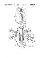
- FIG. 2ais an exploded perspective view of a structure suitable for use in conjunction with a total number N of amplifiers equal to 6, which provides a low impedance junction point and an impedance transformation to an output terminal.
- elements corresponding to those of FIG. 1are designated by the same reference numeral.
- an elongated conductive housing 208has a cross-sectional shape which defines a hexagon, and includes a central bore 216, the inner surface of which forms the outer conductor of a transmission line, as described below.
- transmission lines 54, 56, 58 and 62are coaxial transmission lines which include a semirigid outer conductor, a dielectric material and a coaxial inner conductor.
- transmission line 54includes an outer conductor 210, dielectric material 212 and center conductor 214.
- the outer conductor of transmission line 56 as illustrated in FIG. 2ais designated 210'
- its dielectricis designated 212'
- its center conductor 214'is designated 210'
- the components of transmission line 58are designated by 210, 212 and 214 with a double prime
- transmission line 62carries a triple prime designation.
- a fifth transmission line 254and a sixth transmission line, which would be hidden behind housing 208, is not illustrated.
- Each flat side of hexagonal housing 208includes a through aperture. Three apertures 215, 215' and 215" are visible. Apertures 215 are dimensioned to clear the outer conductor of coaxial transmission lines 54-60, and 254. Smaller threaded holes (not separately designated) arranged in a square pattern around each aperture 215 accept screws (not illustrated) for fastening flanges illustrated as 252.
- an elongated conductor 218having a diameter smaller than the diameter of bore 216.
- Conductor 218is dimensioned to act in conjunction with the inner surface of bore 216 as the center conductor of a transmission line having a selected impedance.
- Region 62 of conductor 218is the junction and includes a plurality of holes, one of which is designated 220, which are dimensioned for receiving the center conductors of transmission lines 54-62 when the transmission lines are inserted into apertures 215.
- that hole designated 220'receives center conductor 214' of transmission line 56
- hole 220"receives center conductor 214" of transmission line 58.
- a mounting base 222includes a hexagonal portion with mounting holes, one of which is designated 224, for mounting the structure to a support (not illustrated), and further includes a cylindrical portion 226 having an outer diameter equal to the inside diameter of bore 216.
- Mounting base 222further includes a through central aperture 228 which provides screwdriver access to the interior of bore 216 after assembly. If desired, one or more threaded holes 230 and screws 230' may be provided to captivate mounting flange 222 to housing 208.
- a commercial coaxial connector such as the type known as type Nis illustrated as 240, and is mounted on a hexagonal conductive plate 42 with its center conductor 244 protruding through a central aperture therein.
- Elongated conductor 218includes a tapered end portion 246 and an axial aperture 248 dimensioned to receive center conductor 244 of connector 240. Tapered portion 246 decreases the electrical field strength between transformer 66 and hexagonal plate 242 to avoid corona discharge or multipactor breakdown in reduced ambient pressure environments, and also compensates for capacitive end effects.
- Elongated conductor 218also includes a threaded axial aperture extending from its bottom, and therefore not visible in FIG. 2a, which extends as far as the plane of holes 220.
- a set screw 250is threaded into the bottom aperture.
- Each of transmission lines 54-62, and transmission line 254 and the further transmission lineare each associated with one of conductive flanges 252.
- Each conductive flangeincludes clearance holes for mounting screws (not illustrated) for mounting the flange to a face of housing 208, as described above, and also includes an annular portion adapted for receiving the outer conductor (210) of its associated transmission line.
- FIG. 2aThe arrangement of FIG. 2a is assembled by mounting a flange 252 onto the outer conductor of its associated transmission line as illustrated in conjunction with transmission line 62, and soldering the outer conductor to the annulus of the flange.
- Connector 240is assembled to hexagonal plate 242, and axial upper aperture 248 of elongated conductor 218 is soldered to center conductor 244 of connector 240.
- the assembly of connector 240, plate 242, and elongated conductor 218is lowered into bore 216 until plate 242 contacts the end of housing 208, and plate 242 is then fastened to housing 208 with screws, one of which is illustrated as 254.
- each flange 252should bottom against one of the hexagonal faces of housing 208 as the transmission line dielectric 212 butts against the outer surface of elongated conductor 218.
- the flanges 252are fastened to housing 208, and mounting base 222 is fastened in place. Screw 250 is then tightened with a screwdriver inserted through hole 228 in support flange 222 to capture the center conductors such as 214 within elongated conductor 218.
- FIG. 2bis a perspective view of an alternative configuration of elongated conductor 218 of FIG. 2a.
- Elongated conductor of FIG. 2bis designated 298 to distinguish it from that of FIG. 2a.
- Conductor 298includes the tapered portion 296 corresponding to tapered portion 246 of elongated conductor 218, and further includes an aperture 295 corresponding in form and function to aperture 248 of conductor 218 of FIG. 2a.
- conductor 298includes a plurality of holes designated 270, 270', 270" . . . located in a manner similar to that of holes 220 of FIG. 2a.
- Conductor 298differs somewhat in structure from conductor 218, and is intended to be capable of dissipating a larger amount of heat, so that it may be used for combining higher powers than the arrangement illustrated in FIG. 2a.
- the ability to dissipate a greater amount of heatis provided by a conductive extension remote from taper 296 and central aperture 295 which includes a necked region 294 dimensioned to fit within aperture 228 of mounting base 222 of FIG. 2a and to make intimate contact therewith.
- a thermally conductive pathextends from junction point 62 through mounting base 222 to the supporting structure (not illustrated).
- the additional portion of conductor 298 which extends from holes 270 to necked portion 294is dimensioned to a length P which is an odd multiple of a quarter wavelength,
- a threaded axial apertureallows screw 250 to capture the center conductors of the various transmission lines as in the arrangement of FIG. 2a.
- FIG. 3is a perspective view, partially exploded, illustrating how the various switches and short-circuited transmission lines are assembled together with the assembly of FIG. 2a.
- elements corresponding to those of FIGS. 1 and 2are designated by the same reference numerals.
- switches 46, 48, 50 and 52, and further switches 346 and 348are arranged in a hexagonal configuration about, and somewhat spaced from, combiner assembly 200.
- the switches and support flange 222 of combiner assembly 200are supported by a support plate (not illustrated).
- Switches 46-348are coaxial SPDT switches such as type DOSQ switches manufactured by Transco Products, Incorporated, of 4241 Glencoe Ave, Venice, Calif. 90291.
- Switch 52as illustrated in FIG. 3 is typical.
- Semirigid coaxial transmission line 60(coax) is connected to the upper surface of switch 52 and is internally connected to the common terminal of the switch.
- Coax 44is connected to one of the switched terminals and, at the remote end as illustrated in FIG. 3, is adapted to be coupled to output terminal 36 of amplifier 28.
- Transmission line 74is connected to the second switched terminal of SPDT switch 52 and extends along a line parallel to the axis 206 of combiner assembly 200. At a selected distance from switch 52, a copper cap 318 is fitted over the outer conductor of coax transmission line 74.
- Cap 318provides a minor amount of adjustment capability which allows the electrical position of the short circuit associated with switch 52 to be precisely set. After it is set in the desired position, the protruding center conductor is soldered to cap 318, and cap 318 is soldered to the outer conductor of coax 74.
- the other switchesare similar to switch 52, and no further description is necessary.
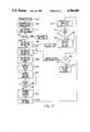
- FIG. 4is a block diagram illustrating a portion of the arrangement of FIG. 1, and includes details of the control arrangement.
- output terminal 30 of amplifier 22is coupled to a signal sampler, which as illustrated is a directional coupler 410.
- Coupler 410has its through path coupled between portions 38' and 38" of transmission line 38, and couples slightly attenuated signal to switch 46.
- Coupler 410also couples a small sample of the signal to a detector 418, which converts the signal nto a direct voltage, the amplitude of which is responsive to the signal power produced at output 30 of amplifier 22.
- the direct voltageis applied from detector 418 to an analog-to-digital converter (ADC) 426, which converts the direct voltage into a corresponding set of binary numbers (a digital signal).
- ADCanalog-to-digital converter
- the digital signalis applied to control logic illustrated as a block 450.
- a directional coupler 412 interposed between portions 40' and 40" of transmission line 40samples the output signal from amplifier 24, and applies the sample to a detector 420 for producing an analog power-responsive voltage, which is converted by ADC 428 into a digital signal for application to control logic 450.
- Other directional couplers 414 and 416coact with detectors 422 and 424, respectively, and with ADC 430 and 432, respectively, to produce digital signals which control logic 450 uses to determine the operating status of the amplifiers.
- Control logic 450processes the signals and generates control signals which establish the operating state of switches 46-52 and (by connections which are not illustrated) the energization of amplifiers 22-28.
- FIG. 5is a simplified flow chart illustrating one possible flow of control logic in control logic 450 of FIG. 4.
- the logicbegins with a command 506 to turn on the composite amplifier ("transmitter").
- the logicproceeds to block 508, where the operating mode is determined by examining the state of a PRESET/MANUAL command.
- a failure register internal to control logic 450(FIG. 4) has a memory location assigned to each amplifier (thus, when there are six amplifiers, there are six memory locations).
- the states F of these memory locationsare initially set to logic zero, representing no failure (all amplifiers are in operating condition or "good”).
- the logicproceeds to a decision block 512, in which the operating mode directs the logic.
- the manual setting inputsare read, as represented by a block 514. These manual settings select those M ⁇ N amplifiers which will initially be on-line.
- the manual settingsset the on-line register in logic block 516. In the preset mode, the logic flows directly from decision block 512 to block 516, retaining the current on-line register setting.
- a block 518which represents the setting of those switches from among switches 46-52 associated with on-line amplifiers to the through position (common terminal coupled to the upper switched terminal, as illustrated in FIG. 1).
- the logicproceeds to a block 520, representing the setting of the remaining switches from among switches 46-52 to the short-circuit condition (common terminal connected to the lower switched terminal, as illustrated in FIG. 1). All change of state of switches 46-52 is performed with the amplifiers deenergized, in one embodiment of the invention, because of limitations on the amount of power which can be reliably switched. For this reason, block 522 represents the energization of the on-line amps.
- the composite amplifieris in its normal operating state, with M amplifiers operating on-line, with their outputs coupled to combiner 200, and the N-M remaining amplifiers waiting in a deenergized state for activation in the event of failure among the on-line amps.
- the switches associated with the off-line amplifiersare in the position coupling the short-circuited transmission line to the combining point, whereby the short-circuit reflects an open-circuit to the combining point. In this condition, the impedance at output terminal 64 of FIG. 1 is the desired Z 1 .
- the logicmonitors the operating state of each of the on-line amplifiers, as represented by block 524.
- This blockrepresents monitoring of the output power of each amplifier, and in order to prevent a drop in output power from being erroneously interpreted as a failure, the output signal power is correlated with input signal power and amplifier power-supply voltage.
- the logic represented by block 524is a separate loop (not illustrated). The logic recurrently flows through a decision block 526, which returns the logic flow to block 524 so long as the output power is satisfactory.
- decision block 526directs the logic to a block 528, which increments the value F of the failure register to F+1, representing the placing in use of one of the N-M spare amplifiers. All the amplifiers are deenergized in block 530, and the failed amplifier is removed from the on-line register in block 532.
- Decision block 534determines whether any spare amplifiers remain by comparing the current value of F with N-(M-1). If F is less than N-(M-1), the YES output of decision block 534 directs the logic to block 536, in which the designation of the next spare in sequence is added to the on-line register. The logic flows from block 536 back to block 518, in which the procedure of bringing the on-line amps to operating status is begun, to bring the composite amplifier to a configuration with a full complement of amplifiers in operation, to provide full power operation.
- the NO output of decision block 534directs the logic to a further decision block 538, in which the current value of F is compared with N, the total number of amplifiers available. So long as F does not equal N, there are still operable amplifiers available, so that at least a reduced-power configuration can be achieved. If F ⁇ N, the NO output of decision block 538 directs the logic to block 518 to begin turn-on in the reduced power configuration. The YES output of decision block 538 (all amplifiers failed) turns off the now-useless composite amplifier to conserve power.
- the logic flow described in conjunction with FIG. 5may be autonomous, or may include stops for human approval or decision.
- the control logicmay be physically located remotely, as on a satellite, for the control of the satellite transmitter, or may be located at a ground station and connected to the composite amplifier by telemetry links.
- switchessuch as switch 46 of FIG. 1 may be located at a position such that the length of short-circuited transmission line 68 of FIG. 1 has an effective length near zero, whereby the length of transmission line 54 of FIG. 1 (plus the electrical length of switch 46) is an odd multiple of one-quarter wavelength.
- other types of impedance transformersmay be used instead of a quarter wavelength transmission line having an impedance ⁇ Z 1 Z 2 , as described in conjunction with FIG. 2a.
- a stepped or continuous-taper transmission linemay be used, as known in the art, or a discrete transformer with primary and secondary windings may be appropriate for certain frequency ranges and bandwidths.
Landscapes
- Engineering & Computer Science (AREA)
- Power Engineering (AREA)
- Amplifiers (AREA)
- Microwave Amplifiers (AREA)
Abstract
Description
Z.sub.2 =Z.sub.1 /M (1)
L=(2N+1)λ/4 (2)
Z.sub.0 =√Z.sub.1 A.sub.2 (3)
P=(2L+1)λ/4 (tm) (4)
Claims (11)
Priority Applications (2)
| Application Number | Priority Date | Filing Date | Title |
|---|---|---|---|
| US07/027,927US4780685A (en) | 1987-03-19 | 1987-03-19 | Composite power amplifier with redundancy |
| JP63062089AJP2675327B2 (en) | 1987-03-19 | 1988-03-17 | Complex power amplifier device |
Applications Claiming Priority (1)
| Application Number | Priority Date | Filing Date | Title |
|---|---|---|---|
| US07/027,927US4780685A (en) | 1987-03-19 | 1987-03-19 | Composite power amplifier with redundancy |
Publications (1)
| Publication Number | Publication Date |
|---|---|
| US4780685Atrue US4780685A (en) | 1988-10-25 |
Family
ID=21840568
Family Applications (1)
| Application Number | Title | Priority Date | Filing Date |
|---|---|---|---|
| US07/027,927Expired - Fee RelatedUS4780685A (en) | 1987-03-19 | 1987-03-19 | Composite power amplifier with redundancy |
Country Status (2)
| Country | Link |
|---|---|
| US (1) | US4780685A (en) |
| JP (1) | JP2675327B2 (en) |
Cited By (44)
| Publication number | Priority date | Publication date | Assignee | Title |
|---|---|---|---|---|
| US4893093A (en)* | 1989-02-02 | 1990-01-09 | United Technologies Incorporated | Switched power splitter |
| WO1990007235A1 (en)* | 1988-12-13 | 1990-06-28 | Stern Telecommunications Corporation | Cable systems or the like |
| US4965527A (en)* | 1989-09-20 | 1990-10-23 | Hughes Aircraft Company | Gain equalizer for microwave balanced amplifier configuration |
| US4965530A (en)* | 1989-09-26 | 1990-10-23 | General Electric Company | Parallelled amplifier with switched isolation resistors |
| US5017888A (en)* | 1989-03-01 | 1991-05-21 | Messerschmitt-Boelkow-Blohm Gmbh | Broadband nonlinear drive control network for linear amplifiers arranged in several amplifier channels |
| EP0690560A1 (en)* | 1994-06-29 | 1996-01-03 | Harris Corporation | Modulator having encoder for fault-adaptive pulse step modulator |
| US5543751A (en)* | 1995-07-21 | 1996-08-06 | Motorola, Inc. | Power combiner for use in a radio frequency system and a method of constructing a power combiner |
| US5610556A (en)* | 1995-10-31 | 1997-03-11 | Space Systems/Loral, Inc. | Multi-port amplifiers with switchless redundancy |
| WO1997034369A1 (en)* | 1996-03-11 | 1997-09-18 | The Mitre Corporation | Pulse waveform generator |
| WO1998001946A1 (en)* | 1996-07-05 | 1998-01-15 | Clifford Harris | Controller-based radio frequency amplifier module and method |
| WO1998029941A1 (en)* | 1996-12-30 | 1998-07-09 | Samsung Electronics Co., Ltd. | Combined linear power amplifying device and method |
| FR2760154A1 (en)* | 1997-02-21 | 1998-08-28 | Lockheed Corp | SPACE ENGINE WITH REDUNDANCY OF PARALLEL AMPLIFIERS |
| US5821811A (en)* | 1995-10-04 | 1998-10-13 | Allgon Ab | Bypass device in an amplifier unit |
| US5831479A (en)* | 1996-06-13 | 1998-11-03 | Motorola, Inc. | Power delivery system and method of controlling the power delivery system for use in a radio frequency system |
| US5872491A (en)* | 1996-11-27 | 1999-02-16 | Kmw Usa, Inc. | Switchable N-way power divider/combiner |
| EP0964511A1 (en)* | 1998-06-11 | 1999-12-15 | Ace Technology | Low-noise amplifier |
| US6154682A (en)* | 1997-07-23 | 2000-11-28 | Lg Information & Communications, Ltd. | Self-checking circuit in microwave equipment |
| WO2001063756A1 (en)* | 2000-02-24 | 2001-08-30 | Wireless Systems International Limited | A signal combiner, a signal splitter and a circuit using a combiner and a splitter |
| US6292677B1 (en)* | 1997-06-26 | 2001-09-18 | Motorola, Inc. | Power delivery system and method of controlling the power delivery system for use in a radio frequency system |
| US6294955B1 (en)* | 2000-04-07 | 2001-09-25 | Harris Corporation | Apparatus and method for use in disconnecting and/or replacing one of a plurality of power amplifiers in a transmitter while the transmitter is operating |
| RU2175809C2 (en)* | 1995-12-27 | 2001-11-10 | Квэлкомм Инкорпорейтед | High-efficiency power amplifier with parallel stages |
| RU2177205C2 (en)* | 1996-12-30 | 2001-12-20 | Самсунг Электроникс Ко., Лтд. | Device and method of integrated linear amplification of power |
| US6518856B1 (en)* | 1999-10-13 | 2003-02-11 | Signal Technology Corporation | RF power divider/combiner circuit |
| RU2199842C2 (en)* | 2000-08-28 | 2003-02-27 | Акционерное общество открытого типа "Приаргунское производственное горно-химическое объединение" | Hot-sparing amplifier being diagnosed |
| US6590448B1 (en) | 2000-09-01 | 2003-07-08 | Texas Instruments Incorporated | Operational amplifier topology and method |
| US20030134595A1 (en)* | 2002-01-11 | 2003-07-17 | Dicamillo Nicholas F. | Optimization of eirp via efficient redundancy pooling concepts |
| WO2002071605A3 (en)* | 2001-03-06 | 2004-02-12 | Andrew Corp | Adaptive power amplifier system |
| US20060125558A1 (en)* | 2004-12-14 | 2006-06-15 | Hodgetts Michael W | Radio frequency power amplifier for lossless power combining |
| US7492313B1 (en) | 2006-10-31 | 2009-02-17 | Lockheed Martin Corporation | Digital processing radar system |
| US20100127783A1 (en)* | 2006-11-03 | 2010-05-27 | International Business Machines Corporation | Switching low noise amplifier |
| US7876261B1 (en) | 2008-10-28 | 2011-01-25 | Lockheed Martin Corporation | Reflected wave clock synchronization |
| US20110254630A1 (en)* | 2008-12-31 | 2011-10-20 | Nxp B.V. | Power amplifier protection |
| US8345716B1 (en) | 2007-06-26 | 2013-01-01 | Lockheed Martin Corporation | Polarization diverse antenna array arrangement |
| US20130043871A1 (en)* | 2011-08-19 | 2013-02-21 | Samsung Electronics Co., Ltd. | Method and apparatus for controlling an amplifier of a magnetic resonance imaging device |
| EP2582039A3 (en)* | 2011-09-19 | 2014-04-16 | Infineon Technologies AG | System and method for generating a radio frequency pulse-width modulated signal |
| US8854255B1 (en) | 2011-03-28 | 2014-10-07 | Lockheed Martin Corporation | Ground moving target indicating radar |
| US8878622B2 (en) | 2011-04-07 | 2014-11-04 | Infineon Technologies Ag | System and method for generating a pulse-width modulated signal |
| WO2015099560A1 (en)* | 2013-12-24 | 2015-07-02 | Siemens Research Center Limited Liability Company | Arrangement and method for rf high power generation |
| CN106063126A (en)* | 2014-01-24 | 2016-10-26 | 西门子有限责任公司 | Arrangement and method for RF high power generation able to compensate a power amplifier module with failure |
| US9509034B2 (en)* | 2014-11-17 | 2016-11-29 | City University Of Hong Kong | N-way coaxial waveguide power divider/combiner |
| RU181024U1 (en)* | 2017-12-08 | 2018-07-03 | Акционерное общество "Научно-исследовательский институт технической физики и автоматизации" (АО "НИИТФА") | RF combiner design with keys |
| EP3384600A1 (en)* | 2015-11-30 | 2018-10-10 | Thales | Switching circuit, and associated stage and amplification and/or division apparatus |
| EP3742609A1 (en)* | 2019-05-22 | 2020-11-25 | Rohde & Schwarz GmbH & Co. KG | Method of operating an amplifier device and amplifier device |
| WO2023232624A1 (en)* | 2022-05-30 | 2023-12-07 | TRUMPF Hüttinger GmbH + Co. KG | Rf combiner arrangement for an rf amplifier arrangement for a particle accelerator, an rf amplifier arrangement of this type, and a particle accelerator of this type |
Families Citing this family (3)
| Publication number | Priority date | Publication date | Assignee | Title |
|---|---|---|---|---|
| US6213442B1 (en)* | 1998-10-08 | 2001-04-10 | Lord Corporation | Isolation system for isolation tables and the like |
| JP6950480B2 (en)* | 2017-11-15 | 2021-10-13 | 日本電気株式会社 | High frequency power synthesizer management method and line short circuit cap |
| JP6982325B2 (en)* | 2019-04-01 | 2021-12-17 | クリオエレクトラ ゲゼルシャフト ミット ベシュレンクテル ハフツングCryoelectra GmbH | High frequency amplification unit with amplification module located on the outer conductor |
Citations (4)
| Publication number | Priority date | Publication date | Assignee | Title |
|---|---|---|---|---|
| US4285346A (en)* | 1979-03-14 | 1981-08-25 | Harry V. LeVeen | Electrode system |
| US4315222A (en)* | 1980-03-06 | 1982-02-09 | Bell Telephone Laboratories, Incorporated | Power combiner arrangement for microwave amplifiers |
| US4641106A (en)* | 1985-05-21 | 1987-02-03 | Rca Corporation | Radial power amplifier |
| US4697160A (en)* | 1985-12-19 | 1987-09-29 | Hughes Aircraft Company | Hybrid power combiner and amplitude controller |
- 1987
- 1987-03-19USUS07/027,927patent/US4780685A/ennot_activeExpired - Fee Related
- 1988
- 1988-03-17JPJP63062089Apatent/JP2675327B2/ennot_activeExpired - Lifetime
Patent Citations (4)
| Publication number | Priority date | Publication date | Assignee | Title |
|---|---|---|---|---|
| US4285346A (en)* | 1979-03-14 | 1981-08-25 | Harry V. LeVeen | Electrode system |
| US4315222A (en)* | 1980-03-06 | 1982-02-09 | Bell Telephone Laboratories, Incorporated | Power combiner arrangement for microwave amplifiers |
| US4641106A (en)* | 1985-05-21 | 1987-02-03 | Rca Corporation | Radial power amplifier |
| US4697160A (en)* | 1985-12-19 | 1987-09-29 | Hughes Aircraft Company | Hybrid power combiner and amplitude controller |
Non-Patent Citations (2)
| Title |
|---|
| Moody et al., "Redundancy Switching of Amplifiers in Satellites", RCA Technical Notes, TN No. 1182, Jun. 10, 1977. |
| Moody et al., Redundancy Switching of Amplifiers in Satellites , RCA Technical Notes, TN No. 1182, Jun. 10, 1977.* |
Cited By (65)
| Publication number | Priority date | Publication date | Assignee | Title |
|---|---|---|---|---|
| WO1990007235A1 (en)* | 1988-12-13 | 1990-06-28 | Stern Telecommunications Corporation | Cable systems or the like |
| US4893093A (en)* | 1989-02-02 | 1990-01-09 | United Technologies Incorporated | Switched power splitter |
| US5017888A (en)* | 1989-03-01 | 1991-05-21 | Messerschmitt-Boelkow-Blohm Gmbh | Broadband nonlinear drive control network for linear amplifiers arranged in several amplifier channels |
| US4965527A (en)* | 1989-09-20 | 1990-10-23 | Hughes Aircraft Company | Gain equalizer for microwave balanced amplifier configuration |
| US4965530A (en)* | 1989-09-26 | 1990-10-23 | General Electric Company | Parallelled amplifier with switched isolation resistors |
| EP0690560A1 (en)* | 1994-06-29 | 1996-01-03 | Harris Corporation | Modulator having encoder for fault-adaptive pulse step modulator |
| US5543751A (en)* | 1995-07-21 | 1996-08-06 | Motorola, Inc. | Power combiner for use in a radio frequency system and a method of constructing a power combiner |
| US5821811A (en)* | 1995-10-04 | 1998-10-13 | Allgon Ab | Bypass device in an amplifier unit |
| US5610556A (en)* | 1995-10-31 | 1997-03-11 | Space Systems/Loral, Inc. | Multi-port amplifiers with switchless redundancy |
| RU2175809C2 (en)* | 1995-12-27 | 2001-11-10 | Квэлкомм Инкорпорейтед | High-efficiency power amplifier with parallel stages |
| WO1997034369A1 (en)* | 1996-03-11 | 1997-09-18 | The Mitre Corporation | Pulse waveform generator |
| US5781066A (en)* | 1996-03-11 | 1998-07-14 | The Mitre Corporation | Pulse waveform generator |
| EP0904633A4 (en)* | 1996-06-13 | 2001-12-05 | Motorola Inc | Power delivery system and method of controlling the power delivery system for use in a radio frequency system |
| US5831479A (en)* | 1996-06-13 | 1998-11-03 | Motorola, Inc. | Power delivery system and method of controlling the power delivery system for use in a radio frequency system |
| US5867060A (en)* | 1996-06-13 | 1999-02-02 | Motorola, Inc. | Power delivery system and method of controlling the power delivery system for use in a radio frequency system |
| WO1998001946A1 (en)* | 1996-07-05 | 1998-01-15 | Clifford Harris | Controller-based radio frequency amplifier module and method |
| US6055418A (en)* | 1996-07-05 | 2000-04-25 | Thomcast Communications, Inc. | Computer program product configured to control modular transmission system components |
| US6078222A (en)* | 1996-07-05 | 2000-06-20 | Thomcast Communications, Inc. | Controller-based radio frequency amplifier module and method |
| US6023612A (en)* | 1996-07-05 | 2000-02-08 | Thomcast Communications, Inc. | Modular transmission system and method |
| US5872491A (en)* | 1996-11-27 | 1999-02-16 | Kmw Usa, Inc. | Switchable N-way power divider/combiner |
| RU2177205C2 (en)* | 1996-12-30 | 2001-12-20 | Самсунг Электроникс Ко., Лтд. | Device and method of integrated linear amplification of power |
| AU733748B2 (en)* | 1996-12-30 | 2001-05-24 | Samsung Electronics Co., Ltd. | Combined linear power amplifying device and method |
| WO1998029941A1 (en)* | 1996-12-30 | 1998-07-09 | Samsung Electronics Co., Ltd. | Combined linear power amplifying device and method |
| FR2760154A1 (en)* | 1997-02-21 | 1998-08-28 | Lockheed Corp | SPACE ENGINE WITH REDUNDANCY OF PARALLEL AMPLIFIERS |
| US6292677B1 (en)* | 1997-06-26 | 2001-09-18 | Motorola, Inc. | Power delivery system and method of controlling the power delivery system for use in a radio frequency system |
| US6154682A (en)* | 1997-07-23 | 2000-11-28 | Lg Information & Communications, Ltd. | Self-checking circuit in microwave equipment |
| EP0964511A1 (en)* | 1998-06-11 | 1999-12-15 | Ace Technology | Low-noise amplifier |
| US6208203B1 (en) | 1998-06-11 | 2001-03-27 | Ace Technology | Low-noise amplifier |
| US6518856B1 (en)* | 1999-10-13 | 2003-02-11 | Signal Technology Corporation | RF power divider/combiner circuit |
| WO2001063756A1 (en)* | 2000-02-24 | 2001-08-30 | Wireless Systems International Limited | A signal combiner, a signal splitter and a circuit using a combiner and a splitter |
| US20030107453A1 (en)* | 2000-02-24 | 2003-06-12 | Peter Kenington | Signal combiner, a signal splitter and a circuit using a combiner and a splitter |
| GB2359666B (en)* | 2000-02-24 | 2004-06-23 | Wireless Systems Int Ltd | A signal combiner, a signal splitter and a circuit using a combiner and a splitter |
| US6844793B2 (en) | 2000-02-24 | 2005-01-18 | Andrew Corporation | Signal combiner, a signal splitter and a circuit using a combiner and a splitter |
| US6294955B1 (en)* | 2000-04-07 | 2001-09-25 | Harris Corporation | Apparatus and method for use in disconnecting and/or replacing one of a plurality of power amplifiers in a transmitter while the transmitter is operating |
| RU2199842C2 (en)* | 2000-08-28 | 2003-02-27 | Акционерное общество открытого типа "Приаргунское производственное горно-химическое объединение" | Hot-sparing amplifier being diagnosed |
| US6590448B1 (en) | 2000-09-01 | 2003-07-08 | Texas Instruments Incorporated | Operational amplifier topology and method |
| US6744312B2 (en)* | 2001-03-06 | 2004-06-01 | Andrew Corporation | Adaptive power amplifier system |
| WO2002071605A3 (en)* | 2001-03-06 | 2004-02-12 | Andrew Corp | Adaptive power amplifier system |
| US20030134595A1 (en)* | 2002-01-11 | 2003-07-17 | Dicamillo Nicholas F. | Optimization of eirp via efficient redundancy pooling concepts |
| US20060125558A1 (en)* | 2004-12-14 | 2006-06-15 | Hodgetts Michael W | Radio frequency power amplifier for lossless power combining |
| US7161425B2 (en)* | 2004-12-14 | 2007-01-09 | Lucent Technologies Inc. | Radio frequency power amplifier for lossless power combining |
| US7492313B1 (en) | 2006-10-31 | 2009-02-17 | Lockheed Martin Corporation | Digital processing radar system |
| US8130033B2 (en)* | 2006-11-03 | 2012-03-06 | International Business Machines Corporation | Switching low noise amplifier |
| US20100127783A1 (en)* | 2006-11-03 | 2010-05-27 | International Business Machines Corporation | Switching low noise amplifier |
| US8345716B1 (en) | 2007-06-26 | 2013-01-01 | Lockheed Martin Corporation | Polarization diverse antenna array arrangement |
| US7876261B1 (en) | 2008-10-28 | 2011-01-25 | Lockheed Martin Corporation | Reflected wave clock synchronization |
| US20110254630A1 (en)* | 2008-12-31 | 2011-10-20 | Nxp B.V. | Power amplifier protection |
| US8373507B2 (en)* | 2008-12-31 | 2013-02-12 | Nxp B.V. | Power amplifier protection |
| US8854255B1 (en) | 2011-03-28 | 2014-10-07 | Lockheed Martin Corporation | Ground moving target indicating radar |
| US8878622B2 (en) | 2011-04-07 | 2014-11-04 | Infineon Technologies Ag | System and method for generating a pulse-width modulated signal |
| US9337821B2 (en) | 2011-04-07 | 2016-05-10 | Infineon Technologies Ag | System and method for generating a pulse-width modulated signal |
| US20130043871A1 (en)* | 2011-08-19 | 2013-02-21 | Samsung Electronics Co., Ltd. | Method and apparatus for controlling an amplifier of a magnetic resonance imaging device |
| US9086464B2 (en)* | 2011-08-19 | 2015-07-21 | Samsung Electronics Co., Ltd. | Method and apparatus for controlling an amplifier of a magnetic resonance imaging device |
| EP2582039A3 (en)* | 2011-09-19 | 2014-04-16 | Infineon Technologies AG | System and method for generating a radio frequency pulse-width modulated signal |
| US8971398B2 (en) | 2011-09-19 | 2015-03-03 | Infineon Technologies Ag | System and method for generating a radio frequency pulse-width modulated signal |
| WO2015099560A1 (en)* | 2013-12-24 | 2015-07-02 | Siemens Research Center Limited Liability Company | Arrangement and method for rf high power generation |
| US9768745B2 (en) | 2013-12-24 | 2017-09-19 | Ooo Siemens | Arrangement and method for radio-frequency (RF) high power generation |
| CN106063126A (en)* | 2014-01-24 | 2016-10-26 | 西门子有限责任公司 | Arrangement and method for RF high power generation able to compensate a power amplifier module with failure |
| EP3087673A1 (en)* | 2014-01-24 | 2016-11-02 | OOO Siemens | Arrangement and method for rf high power generation able to compensate a power amplifier module with failure |
| US9871489B2 (en) | 2014-01-24 | 2018-01-16 | Siemens Aktiengesellschaft | Arrangement and method for radio-frequency (RF) high power generation for compensating a failed power amplifier module |
| US9509034B2 (en)* | 2014-11-17 | 2016-11-29 | City University Of Hong Kong | N-way coaxial waveguide power divider/combiner |
| EP3384600A1 (en)* | 2015-11-30 | 2018-10-10 | Thales | Switching circuit, and associated stage and amplification and/or division apparatus |
| RU181024U1 (en)* | 2017-12-08 | 2018-07-03 | Акционерное общество "Научно-исследовательский институт технической физики и автоматизации" (АО "НИИТФА") | RF combiner design with keys |
| EP3742609A1 (en)* | 2019-05-22 | 2020-11-25 | Rohde & Schwarz GmbH & Co. KG | Method of operating an amplifier device and amplifier device |
| WO2023232624A1 (en)* | 2022-05-30 | 2023-12-07 | TRUMPF Hüttinger GmbH + Co. KG | Rf combiner arrangement for an rf amplifier arrangement for a particle accelerator, an rf amplifier arrangement of this type, and a particle accelerator of this type |
Also Published As
| Publication number | Publication date |
|---|---|
| JPS63260307A (en) | 1988-10-27 |
| JP2675327B2 (en) | 1997-11-12 |
Similar Documents
| Publication | Publication Date | Title |
|---|---|---|
| US4780685A (en) | Composite power amplifier with redundancy | |
| US10833386B2 (en) | Waveguide transitions for power-combining devices | |
| US4263568A (en) | Large scale low-loss combiner and divider | |
| JP2868600B2 (en) | Frequency operating parallel amplifying device and coupling device | |
| EP2471141B1 (en) | Multi-layer radial power divider/combiner | |
| US4495505A (en) | Printed circuit balun with a dipole antenna | |
| US4755769A (en) | Composite amplifier with efficient power reduction | |
| US6552626B2 (en) | High power pin diode switch | |
| US6518856B1 (en) | RF power divider/combiner circuit | |
| US5880648A (en) | N-way RF power combiner/divider | |
| US4315222A (en) | Power combiner arrangement for microwave amplifiers | |
| US4641106A (en) | Radial power amplifier | |
| US6714169B1 (en) | Compact, wide-band, integrated active module for radar and communication systems | |
| US20020084852A1 (en) | Modular high power solid state amplifier | |
| Belohoubek et al. | 30-way radial power combiner for miniature GaAs FET power amplifiers | |
| JPH0799822B2 (en) | Transponder with selective antenna beam using distributed antenna feed elements | |
| US4189683A (en) | Solid state diode amplifier | |
| US4584543A (en) | Radio frequency switching system using pin diodes and quarter-wave transformers | |
| US4328471A (en) | Bandwidth compensated quarter-wave coupled power combiner | |
| EP0393875A1 (en) | A compact multi-polarized broadband antenna | |
| US4931747A (en) | Microwave power amplifier | |
| US6525650B1 (en) | Electronic switching matrix | |
| US4617539A (en) | Reflective phase shifter | |
| Assal et al. | Fast, Fully-Redundant, 4 GHz, 8× 8 Microwave Switch Matrix for Communications Satellites | |
| US6064288A (en) | Coaxial rotary coupler |
Legal Events
| Date | Code | Title | Description |
|---|---|---|---|
| AS | Assignment | Owner name:RCA CORPORATION, A CORP OF DE. Free format text:ASSIGNMENT OF ASSIGNORS INTEREST.;ASSIGNOR:FERGUSON, DONALD A.;REEL/FRAME:004716/0101 Effective date:19870313 Owner name:RCA CORPORATION, NEW JERSEY Free format text:ASSIGNMENT OF ASSIGNORS INTEREST;ASSIGNOR:FERGUSON, DONALD A.;REEL/FRAME:004716/0101 Effective date:19870313 | |
| AS | Assignment | Owner name:GENERAL ELECTRIC COMPANY Free format text:MERGER;ASSIGNOR:R C A CORPORATION, A CORP. OF DE.;REEL/FRAME:004837/0618 Effective date:19880129 Owner name:GENERAL ELECTRIC COMPANY,STATELESS Free format text:MERGER;ASSIGNOR:R C A CORPORATION, A CORP. OF DE.;REEL/FRAME:004837/0618 Effective date:19880129 | |
| FPAY | Fee payment | Year of fee payment:4 | |
| AS | Assignment | Owner name:MARTIN MARIETTA CORPORATION, MARYLAND Free format text:ASSIGNMENT OF ASSIGNORS INTEREST;ASSIGNOR:GENERAL ELECTRIC COMPANY;REEL/FRAME:007046/0736 Effective date:19940322 | |
| FEPP | Fee payment procedure | Free format text:PAYOR NUMBER ASSIGNED (ORIGINAL EVENT CODE: ASPN); ENTITY STATUS OF PATENT OWNER: LARGE ENTITY | |
| FPAY | Fee payment | Year of fee payment:8 | |
| AS | Assignment | Owner name:LOCKHEED MARTIN CORPORATION, MARYLAND Free format text:ASSIGNMENT OF ASSIGNORS INTEREST;ASSIGNOR:MARTIN MARIETTA CORPORATION;REEL/FRAME:008628/0518 Effective date:19960128 | |
| FEPP | Fee payment procedure | Free format text:PAYOR NUMBER ASSIGNED (ORIGINAL EVENT CODE: ASPN); ENTITY STATUS OF PATENT OWNER: LARGE ENTITY Free format text:PAYER NUMBER DE-ASSIGNED (ORIGINAL EVENT CODE: RMPN); ENTITY STATUS OF PATENT OWNER: LARGE ENTITY | |
| REMI | Maintenance fee reminder mailed | ||
| LAPS | Lapse for failure to pay maintenance fees | ||
| FP | Lapsed due to failure to pay maintenance fee | Effective date:20001025 | |
| STCH | Information on status: patent discontinuation | Free format text:PATENT EXPIRED DUE TO NONPAYMENT OF MAINTENANCE FEES UNDER 37 CFR 1.362 |