US4779229A - Prom with programmable output structures - Google Patents
Prom with programmable output structuresDownload PDFInfo
- Publication number
- US4779229A US4779229AUS06/881,161US88116186AUS4779229AUS 4779229 AUS4779229 AUS 4779229AUS 88116186 AUS88116186 AUS 88116186AUS 4779229 AUS4779229 AUS 4779229A
- Authority
- US
- United States
- Prior art keywords
- signal
- output
- programmable
- prom
- input
- Prior art date
- Legal status (The legal status is an assumption and is not a legal conclusion. Google has not performed a legal analysis and makes no representation as to the accuracy of the status listed.)
- Expired - Lifetime
Links
- 230000015654memoryEffects0.000claimsabstractdescription14
- 230000006870functionEffects0.000claimsdescription12
- 230000001360synchronised effectEffects0.000claimsdescription4
- 239000004020conductorSubstances0.000claims1
- 230000004044responseEffects0.000claims1
- 238000012986modificationMethods0.000description2
- 230000004048modificationEffects0.000description2
- 230000008054signal transmissionEffects0.000description2
- 238000013500data storageMethods0.000description1
- 239000011159matrix materialSubstances0.000description1
- 238000000034methodMethods0.000description1
- 230000005855radiationEffects0.000description1
- 239000004065semiconductorSubstances0.000description1
- 230000036962time dependentEffects0.000description1
Images


Classifications
- H—ELECTRICITY
- H03—ELECTRONIC CIRCUITRY
- H03K—PULSE TECHNIQUE
- H03K19/00—Logic circuits, i.e. having at least two inputs acting on one output; Inverting circuits
- H03K19/02—Logic circuits, i.e. having at least two inputs acting on one output; Inverting circuits using specified components
- H03K19/173—Logic circuits, i.e. having at least two inputs acting on one output; Inverting circuits using specified components using elementary logic circuits as components
- H03K19/177—Logic circuits, i.e. having at least two inputs acting on one output; Inverting circuits using specified components using elementary logic circuits as components arranged in matrix form
- H03K19/17748—Structural details of configuration resources
- H03K19/1776—Structural details of configuration resources for memories
- H—ELECTRICITY
- H03—ELECTRONIC CIRCUITRY
- H03K—PULSE TECHNIQUE
- H03K19/00—Logic circuits, i.e. having at least two inputs acting on one output; Inverting circuits
- H03K19/02—Logic circuits, i.e. having at least two inputs acting on one output; Inverting circuits using specified components
- H03K19/173—Logic circuits, i.e. having at least two inputs acting on one output; Inverting circuits using specified components using elementary logic circuits as components
- H03K19/177—Logic circuits, i.e. having at least two inputs acting on one output; Inverting circuits using specified components using elementary logic circuits as components arranged in matrix form
- H03K19/17704—Logic circuits, i.e. having at least two inputs acting on one output; Inverting circuits using specified components using elementary logic circuits as components arranged in matrix form the logic functions being realised by the interconnection of rows and columns
Definitions
- the present inventionrelates generally to programmable integrated circuit memory devices. More particularly, the present invention relates to a programmable read-only memory (PROM) device having separately programmable output modes.
- PROMprogrammable read-only memory
- PROMprogrammable read-only memory
- the PROM deviceinternally includes a decoder and an addressable array of gates implementing logical functions in a two-level implementation in sum-of-terms form.
- the decodergenerally comprises a fixed AND gate array by which input variables are decoded and output as the terms of a function.
- the addressable arraycomprises OR gates having special internal links that can be fused or severed to form the required circuit paths that "program" the device according to the specifications of the user.
- the connections between the outputs of the decoder and the inputs of the OR gatescan be specified to implement a certain logic program.
- PROM devicesfor implementing logic functions has certain advantages over other programmable integrated circuit memory devices (such as speed of operation and ability to decode all input combinations), a major drawback has been that the type of outputs is limited to either combinatorial, as shown in FIG. 1a, or registered, as shown in FIG. 1b, modes only.
- FIG. 2adepicts a typical, well-known combinatorial logic-type structure 1.
- the state of the fuse link 3will control the gate 5 to invert or not to invert a signal on input 7.
- the output 9is commonly known as a "nonstored” or “nonregistered” signal.
- FIG. 2bdepicts a typical, well-known registered-type structure 11.
- a data storage register 13has a data input D coupled via line 7' to one of the input signals, and an output Q coupled via line 9' to one of the single outputs of the circuit or chip.
- the output as shown in FIG. 1bis commonly known as a "stored” or "registered” signal.
- Combinatorial logic output PROM devicesare useful when there is a large number of possible input combinations or product term outputs, whereas registered logic output PROM devices are useful for sequential logic, viz., where there is a large number of variables involved in the logic function.
- a registered PROM devicecan function as a state machine in which the next output is a function of the present state (stored in the register) and the inputs.
- PROM devicewhich provides the capability of defining and programming the architecture of each output on an individual basis.
- the present inventionprovides a PROM integrated circuit combined with a programmable output structure.
- the output structureis coupled to the PROM circuit outputs and includes programmable circuitry whereby the user can program the output structure to provide nonstored/nonregistered or stored/registered signals or any combination thereof as the output.
- FIG. 1ais a schematic drawing of a typical system architecture of a PROM integrated circuit for implementing nonstored/combinatorial logic functions
- FIG. 1bis a schematic drawing of a typical system architecture of a PROM integrated circuit for implementing stored/registered logic functions
- FIG. 2ais a schematic drawing of a typical output structure for a PROM integrated circuit as shown in FIG. 1a;
- FIG. 2bis a schematic drawing of a typical output structure for a PROM integrated circuit as shown in FIG. 1b;
- FIG. 3is a schematic drawing of an exemplary embodiment of the present invention.
- FIG. 4is a schematic drawing of the output structure of the embodiment of the present invention as shown in FIG. 3.
- PROM devicesas depicted in FIGS. 1 and 2, and the implementing specific circuitry, are well-known in the art and are described in detail in many publications. See e.g., Handbook of Semiconductor and Bubble Memories, W. A. Triebel and A. E. Chu, Prentice-Hall, Inc., copyright 1982. As such, no detailed discussion is made herein.
- Embodiments of the output structure used in the present inventionare described in detail in co-pending, partially allowed, U.S. patent application Ser. No. 06/433,253, filed on Oct. 7, 1982, on behalf of the inventors, W. Miller, B. Kitson, and P. Harvey, by the common assignee of the present invention herein. Said application is incorporated by reference herein in its entirety.
- the embodiments described in said co-pending applicationare designed to be used in conjunction with programmable array logic (PAL, a registered trademark of Monolithic Memories, Inc.) or programmable logic array (PLA) integrated circuits which implement familiar sum-of-products logic.
- PALprogrammable array logic
- PPAprogrammable logic array
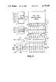
- FIG. 3the combination of a PROM structure with a programmable output structure is shown.
- a 2048 ⁇ 8 bit PROM deviceis shown.
- the present inventioncan be implemented in a multitude of memory size configurations and input/output pin chip carrier packages. Therefore, the specific architecture described herein is not to be understood as any specific limitation on the invention, but only as an example of one embodiment of the general inventive concept.
- the PROM section 2 of the exemplary embodiment of the present inventionhas eleven input lines, A0-A10.
- A0-A3are input to sixteen array column decoder circuit components 4.
- Inputs A4-A10are coupled to one hundred twenty-eight array row decoder circuit components 6.
- the memoryis, for example, a programmable AND array 8 arranged in a 128 ⁇ 128 matrix used to store digital data.
- each row decoder 6Depending on the binary code address bits applied to the input lines A4-A10, each row decoder 6 provides a signal to select one of the rows in the array 8 via input lines 10. Each row decoder 6 thus enables a row to be READ.
- the remaining address input bits A0-A3,are decoded by the column decoders 4.
- the column decoders 4are used to provide signals to a multiplexer 12 via input lines 14.
- the exemplary multiplexer 12has eight units, each having sixteen input terminals coupled to lines 16. Each of the eight multiplexer units has an output terminal for transmitting via output lines 18 the selected one of the sixteen inputs.
- Each column decoder 4thus enables a multiplexer 12 to transmit an eight bit word out of the array 8 via lines 16.
- the data wordsare available for input to the programmable output logic structure 20 via multiplexer output lines 18.
- the output logic structure 20provides eight output cells 22, also referred to as "macrocells,” as shown in FIG. 4.
- a D-type registered flip-flop 24is coupled to multiplexer output lines 18 to receive the PROM section 2 output on its D-input terminal.
- the flip-flop 24is also adapted to receive clock signals via input line 26.
- the Q-output of the flip-flop 24is coupled to a first input of an output logic multiplexer 28 via line 30.
- a second input terminal of each output logic multiplexer 28is coupled directly to a PROM section output line 18 via input line 32.
- each output multiplexer 28 of the macrocell 22includes a programmable fuse link S1.
- each macrocell 22can be programmed to select between the signals on its two input lines 30, 32 for transmitting to the device output via output line 34 through inverter 35 to a chip output pin 00-07.
- the usercan program the macrocell to select for an output to output pins 00-07 between a registered signal via its first input or a nonregistered, viz., combinatorial logic, signal via its second input 32.
- the macrocells 20are fuse programmable. Therefore, once programmed, the output of each macrocell 20 becomes fixed to serve as a combinatorial or registered output. This, however, should not be construed as a limitation on the structure of the invention.
- the macrocell 20could be digitized by replacing the fuse controlled output multiplexer 28 with a signal controlled pass-gate circuitry.
- the macrocell 20could be alternatively used to operate in either the combinatorial or registered output mode at any specific time dependent on the control signal to the passgate circuitry.
- Thiscan offer an ultraviolet radiation erasable PROM or electrically erasable PROM configuration capability.
- the fusescan be replaced by other programmable logic circuit elements to create alternative embodiments which are within the scope of the present invention.
- An output enable circuit 36has an input line 38 coupled to a device input pin for receiving an output enable signal, ENa or ENs.
- the enable signalis provided as an input to a D-type flip-flop 40.
- the enable signalis also sent directly to a device output buffer 42 via flip-flop bypass line 46 through inverter 47.
- a clock pulse for the synchronous mode of operationis provided on a device input pin which is coupled to the macrocells' flip-flop 24 via line 26 through, in this embodiment, inverter 27, as shown in FIG. 4, and to the output enable flip-flop 40 via line 44.
- ENais sent directly to the output buffer via line 46.
- the usercan program the memory section 2 to contain digital data essential to the operational parameters of the system for which the device is used. Moreover, by severing or not severing the fuses S1 of individual cells of the output structure 20, the user is provided the capability of defining and programming the output sent through the output buffer 42 to be registered, combinatorial or a combination of the two.
- the output enable circuitry 36permits the user to choose between synchronous and asynchronous timing.
- This combinationallows the designer to optimize the device design and usage, e.g., by using only as many registers as needed.
- An advantage for the system designeris that only the device of the present invention, rather than separate combinatorial and registered devices, is needed for systems which require both types of logical operation.
Landscapes
- Physics & Mathematics (AREA)
- Mathematical Physics (AREA)
- Engineering & Computer Science (AREA)
- Computer Hardware Design (AREA)
- Computing Systems (AREA)
- General Engineering & Computer Science (AREA)
- Read Only Memory (AREA)
- Design And Manufacture Of Integrated Circuits (AREA)
- Logic Circuits (AREA)
Abstract
Description
Claims (11)
Priority Applications (3)
| Application Number | Priority Date | Filing Date | Title |
|---|---|---|---|
| US06/881,161US4779229A (en) | 1986-07-02 | 1986-07-02 | Prom with programmable output structures |
| EP87305632AEP0252654A3 (en) | 1986-07-02 | 1987-06-24 | Memory device with programmable output structures |
| JP62165148AJPS6325890A (en) | 1986-07-02 | 1987-07-01 | Improved integrated circuit programmable read-only memory device |
Applications Claiming Priority (1)
| Application Number | Priority Date | Filing Date | Title |
|---|---|---|---|
| US06/881,161US4779229A (en) | 1986-07-02 | 1986-07-02 | Prom with programmable output structures |
Publications (1)
| Publication Number | Publication Date |
|---|---|
| US4779229Atrue US4779229A (en) | 1988-10-18 |
Family
ID=25377892
Family Applications (1)
| Application Number | Title | Priority Date | Filing Date |
|---|---|---|---|
| US06/881,161Expired - LifetimeUS4779229A (en) | 1986-07-02 | 1986-07-02 | Prom with programmable output structures |
Country Status (3)
| Country | Link |
|---|---|
| US (1) | US4779229A (en) |
| EP (1) | EP0252654A3 (en) |
| JP (1) | JPS6325890A (en) |
Cited By (9)
| Publication number | Priority date | Publication date | Assignee | Title |
|---|---|---|---|---|
| US5257221A (en)* | 1990-05-15 | 1993-10-26 | Intel Corporation | Apparatus for selecting mumber of wait states in a burst EPROM architecture |
| US5341044A (en)* | 1993-04-19 | 1994-08-23 | Altera Corporation | Flexible configuration logic array block for programmable logic devices |
| US5440246A (en)* | 1994-03-22 | 1995-08-08 | Mosel Vitelic, Incorporated | Programmable circuit with fusible latch |
| US5485104A (en)* | 1985-03-29 | 1996-01-16 | Advanced Micro Devices, Inc. | Logic allocator for a programmable logic device |
| US5666071A (en)* | 1995-12-01 | 1997-09-09 | Advanced Micro Devices, Inc. | Device and method for programming high impedance states upon select input/output pads |
| US5889414A (en)* | 1997-04-28 | 1999-03-30 | Mosel Vitelic Corporation | Programmable circuits |
| US6084803A (en)* | 1998-10-23 | 2000-07-04 | Mosel Vitelic, Inc. | Initialization of non-volatile programmable latches in circuits in which an initialization operation is performed |
| US6163492A (en)* | 1998-10-23 | 2000-12-19 | Mosel Vitelic, Inc. | Programmable latches that include non-volatile programmable elements |
| US6380724B1 (en) | 1999-11-16 | 2002-04-30 | Advanced Micro Devices, Inc. | Method and circuitry for an undisturbed scannable state element |
Families Citing this family (3)
| Publication number | Priority date | Publication date | Assignee | Title |
|---|---|---|---|---|
| WO1999059088A2 (en)* | 1998-05-11 | 1999-11-18 | Koninklijke Philips Electronics N.V. | A programmable logic device with macrocell controlled by a pla |
| JP2006142996A (en)* | 2004-11-19 | 2006-06-08 | Nifco Inc | Valve for fuel tank |
| US7352602B2 (en) | 2005-12-30 | 2008-04-01 | Micron Technology, Inc. | Configurable inputs and outputs for memory stacking system and method |
Citations (5)
| Publication number | Priority date | Publication date | Assignee | Title |
|---|---|---|---|---|
| US4422072A (en)* | 1981-07-30 | 1983-12-20 | Signetics Corporation | Field programmable logic array circuit |
| US4546273A (en)* | 1983-01-11 | 1985-10-08 | Burroughs Corporation | Dynamic re-programmable PLA |
| US4609986A (en)* | 1984-06-14 | 1986-09-02 | Altera Corporation | Programmable logic array device using EPROM technology |
| US4617479A (en)* | 1984-05-03 | 1986-10-14 | Altera Corporation | Programmable logic array device using EPROM technology |
| US4717912A (en)* | 1982-10-07 | 1988-01-05 | Advanced Micro Devices, Inc. | Apparatus for producing any one of a plurality of signals at a single output |
Family Cites Families (1)
| Publication number | Priority date | Publication date | Assignee | Title |
|---|---|---|---|---|
| EP0177280B1 (en)* | 1984-09-28 | 1991-05-29 | Advanced Micro Devices, Inc. | Dynamically controllable output logic circuit |
- 1986
- 1986-07-02USUS06/881,161patent/US4779229A/ennot_activeExpired - Lifetime
- 1987
- 1987-06-24EPEP87305632Apatent/EP0252654A3/ennot_activeWithdrawn
- 1987-07-01JPJP62165148Apatent/JPS6325890A/enactivePending
Patent Citations (6)
| Publication number | Priority date | Publication date | Assignee | Title |
|---|---|---|---|---|
| US4422072A (en)* | 1981-07-30 | 1983-12-20 | Signetics Corporation | Field programmable logic array circuit |
| US4717912A (en)* | 1982-10-07 | 1988-01-05 | Advanced Micro Devices, Inc. | Apparatus for producing any one of a plurality of signals at a single output |
| US4546273A (en)* | 1983-01-11 | 1985-10-08 | Burroughs Corporation | Dynamic re-programmable PLA |
| US4617479A (en)* | 1984-05-03 | 1986-10-14 | Altera Corporation | Programmable logic array device using EPROM technology |
| US4617479B1 (en)* | 1984-05-03 | 1993-09-21 | Altera Semiconductor Corp. | Programmable logic array device using eprom technology |
| US4609986A (en)* | 1984-06-14 | 1986-09-02 | Altera Corporation | Programmable logic array device using EPROM technology |
Cited By (12)
| Publication number | Priority date | Publication date | Assignee | Title |
|---|---|---|---|---|
| US5485104A (en)* | 1985-03-29 | 1996-01-16 | Advanced Micro Devices, Inc. | Logic allocator for a programmable logic device |
| US5257221A (en)* | 1990-05-15 | 1993-10-26 | Intel Corporation | Apparatus for selecting mumber of wait states in a burst EPROM architecture |
| US5341044A (en)* | 1993-04-19 | 1994-08-23 | Altera Corporation | Flexible configuration logic array block for programmable logic devices |
| US5440246A (en)* | 1994-03-22 | 1995-08-08 | Mosel Vitelic, Incorporated | Programmable circuit with fusible latch |
| US5666071A (en)* | 1995-12-01 | 1997-09-09 | Advanced Micro Devices, Inc. | Device and method for programming high impedance states upon select input/output pads |
| US5889414A (en)* | 1997-04-28 | 1999-03-30 | Mosel Vitelic Corporation | Programmable circuits |
| US6084803A (en)* | 1998-10-23 | 2000-07-04 | Mosel Vitelic, Inc. | Initialization of non-volatile programmable latches in circuits in which an initialization operation is performed |
| US6163492A (en)* | 1998-10-23 | 2000-12-19 | Mosel Vitelic, Inc. | Programmable latches that include non-volatile programmable elements |
| US6222776B1 (en) | 1998-10-23 | 2001-04-24 | Mosel Vitelic, Inc. | Programmable latches that include non-volatile programmable elements |
| US6240034B1 (en) | 1998-10-23 | 2001-05-29 | Mosel Vitelic, Inc. | Programmable latches that include non-volatile programmable elements |
| US6266290B1 (en) | 1998-10-23 | 2001-07-24 | Mosel Vitelic, Inc. | Programmable latches that include non-volatile programmable elements |
| US6380724B1 (en) | 1999-11-16 | 2002-04-30 | Advanced Micro Devices, Inc. | Method and circuitry for an undisturbed scannable state element |
Also Published As
| Publication number | Publication date |
|---|---|
| EP0252654A3 (en) | 1989-03-15 |
| JPS6325890A (en) | 1988-02-03 |
| EP0252654A2 (en) | 1988-01-13 |
Similar Documents
| Publication | Publication Date | Title |
|---|---|---|
| US6480025B1 (en) | Driver circuitry for programmable logic devices with hierarchical interconnection resources | |
| US5850151A (en) | Programmable logic array intergrated circuit devices | |
| US5256918A (en) | Programmable logic circuit | |
| US6049225A (en) | Input/output interface circuitry for programmable logic array integrated circuit devices | |
| EP0183828B1 (en) | An improved programmable logic array device using cmos eprom floating gate technology | |
| US4032894A (en) | Logic array with enhanced flexibility | |
| US6020759A (en) | Programmable logic array device with random access memory configurable as product terms | |
| EP1455455B1 (en) | A programmable logic device which stores more than one configuration and means for switching configurations | |
| US4963768A (en) | Flexible, programmable cell array interconnected by a programmable switch matrix | |
| EP0410759B1 (en) | Configurable logic array and method | |
| US4779229A (en) | Prom with programmable output structures | |
| US5349670A (en) | Integrated circuit programmable sequencing element apparatus | |
| US5302866A (en) | Input circuit block and method for PLDs with register clock enable selection | |
| EP0789878A1 (en) | Hierarchical crossbar switch | |
| US20020130681A1 (en) | Programmable logic array integrated circuits | |
| US6344989B1 (en) | Programmable logic devices with improved content addressable memory capabilities | |
| US6556502B2 (en) | Memory circuitry for programmable logic integrated circuit devices | |
| US6356110B1 (en) | Multifunction memory array in a programmable logic device | |
| US5298803A (en) | Programmable logic device having low power microcells with selectable registered and combinatorial output signals | |
| US5760719A (en) | Programmable I/O cell with data conversion capability | |
| US5936426A (en) | Logic function module for field programmable array | |
| US5869982A (en) | Programmable I/O cell with data conversion capability | |
| EP0254479A2 (en) | Integrated circuit programmable sequencing element apparatus and associated method | |
| US5917337A (en) | Programmable I/O cell with data conversion capability | |
| GB2333873A (en) | Programmable logic array |
Legal Events
| Date | Code | Title | Description |
|---|---|---|---|
| AS | Assignment | Owner name:ADVANCED MICRO DEVICES, INC., 901 THOMPSON PLACE, Free format text:ASSIGNMENT OF ASSIGNORS INTEREST.;ASSIGNOR:AGRAWAL, OM P.;REEL/FRAME:004583/0305 Effective date:19860630 Owner name:ADVANCED MICRO DEVICES, INC., A CORP. OF DE.,CALIF Free format text:ASSIGNMENT OF ASSIGNORS INTEREST;ASSIGNOR:AGRAWAL, OM P.;REEL/FRAME:004583/0305 Effective date:19860630 | |
| STCF | Information on status: patent grant | Free format text:PATENTED CASE | |
| FPAY | Fee payment | Year of fee payment:4 | |
| FPAY | Fee payment | Year of fee payment:8 | |
| AS | Assignment | Owner name:VANTIS CORPORATION, CALIFORNIA Free format text:ASSIGNMENT OF ASSIGNORS INTEREST;ASSIGNOR:ADVANCED MICRO DEVICES, INC.;REEL/FRAME:010340/0329 Effective date:19990615 | |
| AS | Assignment | Owner name:VANTIS CORPORATION, CALIFORNIA Free format text:ASSIGNMENT OF ASSIGNORS INTEREST;ASSIGNOR:ADVANCED MICRO DEVICES, INC.;REEL/FRAME:010310/0899 Effective date:19990615 | |
| FEPP | Fee payment procedure | Free format text:PAYOR NUMBER ASSIGNED (ORIGINAL EVENT CODE: ASPN); ENTITY STATUS OF PATENT OWNER: LARGE ENTITY | |
| FPAY | Fee payment | Year of fee payment:12 | |
| FEPP | Fee payment procedure | Free format text:PAYER NUMBER DE-ASSIGNED (ORIGINAL EVENT CODE: RMPN); ENTITY STATUS OF PATENT OWNER: LARGE ENTITY Free format text:PAYOR NUMBER ASSIGNED (ORIGINAL EVENT CODE: ASPN); ENTITY STATUS OF PATENT OWNER: LARGE ENTITY | |
| AS | Assignment | Owner name:LATTICE SEMICONDUCTOR CORPORATION, OREGON Free format text:MERGER;ASSIGNOR:VANTIS CORPORATION;REEL/FRAME:012937/0738 Effective date:20020211 |