US4778693A - Photolithographic mask repair system - Google Patents
Photolithographic mask repair systemDownload PDFInfo
- Publication number
- US4778693A US4778693AUS06/919,975US91997586AUS4778693AUS 4778693 AUS4778693 AUS 4778693AUS 91997586 AUS91997586 AUS 91997586AUS 4778693 AUS4778693 AUS 4778693A
- Authority
- US
- United States
- Prior art keywords
- objective
- gas
- laser
- laser beam
- mask
- Prior art date
- Legal status (The legal status is an assumption and is not a legal conclusion. Google has not performed a legal analysis and makes no representation as to the accuracy of the status listed.)
- Expired - Lifetime
Links
Images


Classifications
- G—PHYSICS
- G03—PHOTOGRAPHY; CINEMATOGRAPHY; ANALOGOUS TECHNIQUES USING WAVES OTHER THAN OPTICAL WAVES; ELECTROGRAPHY; HOLOGRAPHY
- G03F—PHOTOMECHANICAL PRODUCTION OF TEXTURED OR PATTERNED SURFACES, e.g. FOR PRINTING, FOR PROCESSING OF SEMICONDUCTOR DEVICES; MATERIALS THEREFOR; ORIGINALS THEREFOR; APPARATUS SPECIALLY ADAPTED THEREFOR
- G03F1/00—Originals for photomechanical production of textured or patterned surfaces, e.g., masks, photo-masks, reticles; Mask blanks or pellicles therefor; Containers specially adapted therefor; Preparation thereof
- G03F1/68—Preparation processes not covered by groups G03F1/20 - G03F1/50
- G03F1/72—Repair or correction of mask defects
- B—PERFORMING OPERATIONS; TRANSPORTING
- B23—MACHINE TOOLS; METAL-WORKING NOT OTHERWISE PROVIDED FOR
- B23K—SOLDERING OR UNSOLDERING; WELDING; CLADDING OR PLATING BY SOLDERING OR WELDING; CUTTING BY APPLYING HEAT LOCALLY, e.g. FLAME CUTTING; WORKING BY LASER BEAM
- B23K26/00—Working by laser beam, e.g. welding, cutting or boring
- B23K26/14—Working by laser beam, e.g. welding, cutting or boring using a fluid stream, e.g. a jet of gas, in conjunction with the laser beam; Nozzles therefor
- B23K26/144—Working by laser beam, e.g. welding, cutting or boring using a fluid stream, e.g. a jet of gas, in conjunction with the laser beam; Nozzles therefor the fluid stream containing particles, e.g. powder
- C—CHEMISTRY; METALLURGY
- C23—COATING METALLIC MATERIAL; COATING MATERIAL WITH METALLIC MATERIAL; CHEMICAL SURFACE TREATMENT; DIFFUSION TREATMENT OF METALLIC MATERIAL; COATING BY VACUUM EVAPORATION, BY SPUTTERING, BY ION IMPLANTATION OR BY CHEMICAL VAPOUR DEPOSITION, IN GENERAL; INHIBITING CORROSION OF METALLIC MATERIAL OR INCRUSTATION IN GENERAL
- C23C—COATING METALLIC MATERIAL; COATING MATERIAL WITH METALLIC MATERIAL; SURFACE TREATMENT OF METALLIC MATERIAL BY DIFFUSION INTO THE SURFACE, BY CHEMICAL CONVERSION OR SUBSTITUTION; COATING BY VACUUM EVAPORATION, BY SPUTTERING, BY ION IMPLANTATION OR BY CHEMICAL VAPOUR DEPOSITION, IN GENERAL
- C23C16/00—Chemical coating by decomposition of gaseous compounds, without leaving reaction products of surface material in the coating, i.e. chemical vapour deposition [CVD] processes
- C23C16/04—Coating on selected surface areas, e.g. using masks
- C23C16/047—Coating on selected surface areas, e.g. using masks using irradiation by energy or particles
- C—CHEMISTRY; METALLURGY
- C23—COATING METALLIC MATERIAL; COATING MATERIAL WITH METALLIC MATERIAL; CHEMICAL SURFACE TREATMENT; DIFFUSION TREATMENT OF METALLIC MATERIAL; COATING BY VACUUM EVAPORATION, BY SPUTTERING, BY ION IMPLANTATION OR BY CHEMICAL VAPOUR DEPOSITION, IN GENERAL; INHIBITING CORROSION OF METALLIC MATERIAL OR INCRUSTATION IN GENERAL
- C23C—COATING METALLIC MATERIAL; COATING MATERIAL WITH METALLIC MATERIAL; SURFACE TREATMENT OF METALLIC MATERIAL BY DIFFUSION INTO THE SURFACE, BY CHEMICAL CONVERSION OR SUBSTITUTION; COATING BY VACUUM EVAPORATION, BY SPUTTERING, BY ION IMPLANTATION OR BY CHEMICAL VAPOUR DEPOSITION, IN GENERAL
- C23C16/00—Chemical coating by decomposition of gaseous compounds, without leaving reaction products of surface material in the coating, i.e. chemical vapour deposition [CVD] processes
- C23C16/44—Chemical coating by decomposition of gaseous compounds, without leaving reaction products of surface material in the coating, i.e. chemical vapour deposition [CVD] processes characterised by the method of coating
- C23C16/48—Chemical coating by decomposition of gaseous compounds, without leaving reaction products of surface material in the coating, i.e. chemical vapour deposition [CVD] processes characterised by the method of coating by irradiation, e.g. photolysis, radiolysis, particle radiation
- C23C16/483—Chemical coating by decomposition of gaseous compounds, without leaving reaction products of surface material in the coating, i.e. chemical vapour deposition [CVD] processes characterised by the method of coating by irradiation, e.g. photolysis, radiolysis, particle radiation using coherent light, UV to IR, e.g. lasers
- H—ELECTRICITY
- H05—ELECTRIC TECHNIQUES NOT OTHERWISE PROVIDED FOR
- H05K—PRINTED CIRCUITS; CASINGS OR CONSTRUCTIONAL DETAILS OF ELECTRIC APPARATUS; MANUFACTURE OF ASSEMBLAGES OF ELECTRICAL COMPONENTS
- H05K3/00—Apparatus or processes for manufacturing printed circuits
- H05K3/10—Apparatus or processes for manufacturing printed circuits in which conductive material is applied to the insulating support in such a manner as to form the desired conductive pattern
- H05K3/14—Apparatus or processes for manufacturing printed circuits in which conductive material is applied to the insulating support in such a manner as to form the desired conductive pattern using spraying techniques to apply the conductive material, e.g. vapour evaporation
- H05K3/146—By vapour deposition
- H—ELECTRICITY
- H05—ELECTRIC TECHNIQUES NOT OTHERWISE PROVIDED FOR
- H05K—PRINTED CIRCUITS; CASINGS OR CONSTRUCTIONAL DETAILS OF ELECTRIC APPARATUS; MANUFACTURE OF ASSEMBLAGES OF ELECTRICAL COMPONENTS
- H05K3/00—Apparatus or processes for manufacturing printed circuits
- H05K3/22—Secondary treatment of printed circuits
- H05K3/225—Correcting or repairing of printed circuits
- Y—GENERAL TAGGING OF NEW TECHNOLOGICAL DEVELOPMENTS; GENERAL TAGGING OF CROSS-SECTIONAL TECHNOLOGIES SPANNING OVER SEVERAL SECTIONS OF THE IPC; TECHNICAL SUBJECTS COVERED BY FORMER USPC CROSS-REFERENCE ART COLLECTIONS [XRACs] AND DIGESTS
- Y10—TECHNICAL SUBJECTS COVERED BY FORMER USPC
- Y10S—TECHNICAL SUBJECTS COVERED BY FORMER USPC CROSS-REFERENCE ART COLLECTIONS [XRACs] AND DIGESTS
- Y10S430/00—Radiation imagery chemistry: process, composition, or product thereof
- Y10S430/146—Laser beam
Definitions
- This inventionpertains to a method for creating a volume of controlled atmosphere without the use of a full enclosure, and more particularly, to a system which creates a controlled gas atmosphere under any of the microscope objectives mounted on a standard microscope nosepiece. Any of the objectives can then be used to deliver laser radiation of appropriate wavelength and beam shape.
- the systemcan be used to photolytically and/or pyrolytically decompose suitable gaseous materials contained in the gas atmosphere or photoactivate a surface in the microscope objective focus plane to modify the reaction rates between the surface and the surrounding gas.
- This methodallows for exclusion of air from the gas atmosphere.
- a specific source of gaseous atmosphereallowing repairs of clear defects in photolithographic masks used for making electronic integrated circuits.
- Vacuum tight cellswith their associated heat- and fume-producing and noisy vacuum pumps are typically used to facilitate atmospheric control (See for example U.S. Pat. No. 4,340,617, U.S. Pat. No. 4,451,503, U.S. Pat. No. 4,525,379, and U.S. Pat. No. 4,465,529).
- Proper gas mixesare introduced into the cells after evacuation using either a flow-through or sealed-off mode of operation.
- Laser radiationintroduced through a focusing optical system and the cell window, is then typically used to activate the process by decomposing some components of the gas mixture in the gas phase or after adsorption on the surface. The products of decomposition then create deposits or etch effects.
- Substrate activation effectswhich make the locally activated region preferentially susceptible to etch effects by the surrounding gas phase, can also be produced by laser irradiation. Spatial resolution achievable with a given process is typically limited by the fact that the microscope focusing objective has to be able to accommodate cell window thickness. This large working distance usually reduces the numerical aperture (N.A.) to a lower value than might be desirable.
- N.A.numerical aperture
- a principal objective of the present inventionis to provide a method for lowering the cost and improving the throughput and spatial resolution of laser-initiated photolytic and/or pyrolytic reactions by removing the need for providing a gas-tight cell with its associated vacuum equipment.
- a further objectiveis to provide a method and device which allows the use of toxic substances in the process without endangering the operator.
- Another objectiveis to provide a means of protecting the microscope objective from deposits, detrimental to its optical functions, caused by photolytic decomposition processes without the introduction of any extra transparent surfaces which would themselves be in turn exposed to the optically-detrimental deposits.
- Yet another objectiveis to provide a convenient source material to be used in laser driven repairs of clear defects on photolithographic masks.
- Yet another objectiveis to provide a device which can be readily integrated with a device for correcting opaque defects on photolithographic masks which device requires the highest possible numerical aperture microscope objectives for submicron repair capabilities.
- a one- or multi-layer shroudis placed around the particular microscope objective and a stream of process gas is injected under the objective or into one of the shroud volumes.
- the net effectis to replace the air under the objective with the proper mixture of process and buffer gases.
- Ten cc/min. gas flowsare typically sufficient to replace most of the air under a high magnification microscope objective when the gas is directed there by a properly pointed 0.010 in i.d. nozzle.
- One hundred cc/min flowsare typical of shroud filling and area flooding approaches.
- An exhaust systemis then used to pick up all the process gases and the gaseous decomposition products to protect the operators from possibly toxic substances.
- Such an exhaust systemconsists typically of a shroud concentric with the objective and attached to a source of slightly negative pressure, such as a "House vent” or the input to an exhaust fan.
- a source of slightly negative pressuresuch as a "House vent” or the input to an exhaust fan.
- Proper filters and/or neutralizing devicescan be used to make the exhaust safe for emission into the outside air.
- a microscopeutilizes typically a number of objectives of varying magnification. These are usually mounted on a rotating nosepiece. Each of these objectives can be brought into use by rotating the nosepiece. Any and all of the standard objectives can be enclosed by gas-containing-shrouds according to the present invention. Any one of such shrouded microscope objectives can be rotated into the process position and used safely and efficiently.
- a specific system used for clear defect repair on photolithographic masksconsists of such a shroud-surrounded microscope objective delivering a focused 488 nanometer wavelength beam from an Argon laser to the surface of a photolithographic mask.
- the interaction of this approximately 10 milliwatt beam, focused to about 1 micrometer diameter, with a metal feature on the maskproduces a high temperature spot. This spot becomes the starting point for pyrolytic decomposition, similar to the method of U.S. Pat. No. 4,543,270.
- the metal film deposits produced by this methodwhen extended over adjacent clear (missing chrome) defect areas, make these clear areas opaque, thus effecting the repair.
- a mixture of sublimed phases of hexacarbonyls of chromium and molybdenumis carried to the objective area by a nonoxidizing carrier gas, e.g. Argon, and serves as a source for the metal deposits.
- a nonoxidizing carrier gase.g. Argon
- Molybdenumprovides better quality deposited films while chromium provides improved resistance to the typical chemical cleaning agents, such as hot mixtures of chromic and sulfuric acids, used in processing of photolithographic masks.
- a venting arrangementdrawing in about 2 cubic feet per minute of ambient air, together with the process gases and their by-products, is used as described above to keep these toxic gases away from the operator.
- the effluentsare processed through activated charcoal filters to remove the remnants of toxic gases before they are emitted into the house vent.
- N.A.Numerical Aperture
- the present inventionby allowing windowless clear defect repair, preserves the high resolution opaque repair capability on the same system. Further advantage is provided by dispensing with the need for vacuum hardware and pumps and the reduction in throughput associated with making and breaking of vacuum tight seals for insertion and removal of the mask into and out of the cell.
- the specific objective protection scheme for photolytic processesinvolves a similar setup to that for pyrolysis but includes an extra chamber 132 in FIG. 10 or the inner, open chamber of reflective objective in FIG. 11 with a hole through which a small amount of buffer gas alone, e.g. Argon gas, is supplied through 158 to keep the decomposable components of process gas away from sensitive surfaces. Flow rates are adjusted so that the extra buffer gas flow does not displace too much of the process gas in the microscope focal region. A 5cc/min extra buffer gas flow is typical for a 3 mm diameter opening (138 in FIG. 10).
- a reflective objectiveis used instead of a refractive one, as is frequently the case when using ultraviolet light sources, the objective itself can be flooded by the gentle flow of buffer gas to protect its reflective surfaces from the process gas.
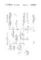
- FIG. 1shows an optical schematic diagram for a combined clear and opaque defect correcting system constructed in accordance with the invention
- FIG. 2shows a schematic view of an initial embodiment of the invention
- FIG. 3shows a schematic view of an alternate embodiment of the invention
- FIG. 4shows a side-sectional view of a mask repaired in accordance with this invention
- FIG. 5shows a partial plan view of a mask with clear defects
- FIG. 6shows a partial plan view of the mask of FIG. 5 immediately after the clear defects have been corrected in accordance with this invention
- FIG. 7shows details of a microscope and shroud in accordance with the embodiment of FIG. 2;
- FIG. 8shows details of a microscope shroud in accordance with the embodiment of FIG. 3;
- FIG. 9shows a side view of a microscope with a shroud shown in FIG. 3;
- FIG. 10shows a schematic view of a third embodiment of the invention with means for protecting the microscope objective
- FIG. 11shows a schematic view of a fourth embodiment of the invention wherein a reflective-type microscope objective is used.
- FIG. 1A combined mask correcting system for clear and opaque defects shall now be described in conjunction with FIG. 1; however, it should be understood that, except as noted, a system for correcting only clear defects would be essentially identical.
- a mask-defect correcting system 10having three lasers: an argon laser 12 operated at 488 nm, a helium-neon 633 nm pointing laser 14, and an Nd:YAG laser 16 operated at 1064 nm.
- a mirror 18directs the output of Nd:YAG laser 16 to a Second Harmonic Generator crystal 20 which in response generates a coherent beam at 532 nm.
- the beams from lasers 12, 14 and crystal 20are directed by a common optical beam delivery system 22, containing a number of lenses used to adjust the size and divergence of the various laser beams, along a common axis, serially to a mirror 24, repair aperture 26, focusing lens 28, mirror 30 and objective lens 32 which focuses the beams onto mask 34.
- Laser 14is provided to show the location of a laser 12 beam, not visible due to safety filter 42, on the mask.
- a spot marker (an incoherent tungsten-halogen source) 36is included to indicate a target spot on the mask for opaque defect repair.
- tungsten-halogen light source 38Light from a tungsten-halogen light source 38 is used to illuminate mask 34 from below via mirror 40 and condenser lens 41 so that the opaque and clear regions of the mask are clearly visible in ocular 50.
- Mirror 30is semi-transparent so that the image of the mask is transmitted upwards through mirror 30, a safety filter 42, to a video camera 44.
- the picture generated by video camera 44is displayed by video monitor 46. Between filter 42 and camera 44 a second semi-transparent mirror 48 also projects the image of the mask toward ocular lens 50 for direct viewing. If a beam having a specific shape (i.e. rectangular) is required, aperture 26 may be shaped accordingly.
- Objective lens 32may be selected to have a magnification of for example 5 ⁇ , 20 ⁇ , 50 ⁇ or 100 ⁇ .
- argon laser 12is used depending on the particular defect on mask 34. More particularly, for an opaque defect, the frequency doubled output of the Nd:Y laser is used to vaporize the unwanted opaque film on the mask. For clear defects, argon laser 12 is used as described below.
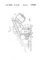
- a typical 100 microscope objective 52is used to direct combined laser beams 54 to mask 34.
- the objectiveis typically disposed at a working distance of about 0.012 in. from the mask.
- a shroud 56envelopes the objective and the immediate area of the mask surrounding the work area, i.e. the region of the mask with a defect.
- the shroud 56is penetrated by an exhaust pipe 60.
- Delivery pipe 58is connected to a container 62 which may contain a premixed gaseous compound including both organometallic compounds and a carrier/buffer gas. Alternatively, container 62 may contain only the organometallic compounds, in which case a pipe 64 may be used to provide the buffer/carrier gas. Pipe 58 brings the process gas mixture to the volume between objective 52 and mask 34.
- the process gas (PG)preferably comprises a mixture of the sublimated phase of hexacarbonyls of chromium and molybdenum [Cr(Co) 6 and Mo(Co) 6 ] at or near room temperature.
- Chromiumhas been included because it typically forms the opaque patterns on the mask as manufactured.
- chromium depositsresist all normal mask cleaning procedures.
- laser-deposited chromiumtends to form granular films.
- Laser-deposited molybdenumforms smoother films but pure molybdenum deposits are easily removed by normal mask-cleaning processes. It was found that the combination of chromium and molybdenum compounds produces films which retain the good properties of the individual deposits. Both metal carbonyls are crystalline in nature, have a low vapor pressure at room temperature and therefore are easy to handle.
- the buffer/carrier gasis used as a means to propel the vapor phases of the organometallic compounds into the shroud at atmospheric pressure.
- the buffer/carrier gasmay include helium, argon, nitrogen, etc. While air has also been used successfully, it was found that it is somewhat less effective in producing uniform metallic deposits than the previously mentioned gases.
- PG compositionconsisting of nearly saturated vapor phases of the carbonyls near room temperature
- the gas mixture described aboveis fed through pipe 58 into the region lying between the mask 34 and objective 52.
- the Argon laser beam 54When the Argon laser beam 54 is activated for a period of a few seconds, its focused beam heats approximately one square micrometer area of the surface of mask 34 to above 150° C., causing the hexacarbonyls to decompose at that spot, thereby forming a metallic layer on mask 34.
- Unused PG, buffer/carrier gas and the gases produced by the decompositionare removed through pipe 60.
- the concentration of the delivered gas mixture in the volume between the objective 52 and mask 34is dependent on the exact orientation of pipe 58.
- FIG. 3alleviates that dependence as follows.
- a cylindrical chamber 66is formed within the shroud 56 to contain the gas from pipe 58 within the immediate vicinity of objective 52 and mask 34 and deliver it with approximately cylindrical symmetry as shown.
- An annular chamber 68is then formed between shroud 56 and inner chamber 66 in which the exhaust gases can collect before being removed through pipe 60.
- mask 34includes a transparent quartz substrate 70 with a chrome-based opaque layer 72, said layer containing a transparent opening 74. Opening 74 is covered by added portion 76 which comprises a mixture of chromium and molybdenum in accordance with the present invention.
- portion 76partially overlaps layer 72 as shown, so that said portion is bonded not only to the substrate 70 but also to the layer 72.
- portion 76remains firmly attached to the mask.
- a mask treated in accordance with this inventionwas subjected to immersion in hot and cold RT2* (chromic sulfuric acid mixture), hand scrubbing, and cleaning in Ultratech Model 602 and 603 plate cleaners operating at pressures up to 2400 psi.
- the corrected clear defectspassed standard optical inspection both before and after cleaning.
- FIGS. 5-6some actual clear faults and their correction according to this invention are illustrated.
- an opaque strip 80 on a substrate(not shown) said strip having two types of clear faults: a micrometer size pin-hole 84 and a so-called mouse nip 86 extending a few tenth of a micrometer into strip 80.
- FIG. 6shows the strip 80 after patches have been applied to the faults as described above. The edge 88 was trimmed using YAG laser 16 and beam shaping aperture 26.
- the above described processcan be used to form a continuous deposition strip by feeding gas continuously to the shroud and moving the mask under the focused beam (or vice-versa) in a raster scan pattern to cover the defect.
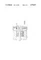
- FIG. 7shows the details of shroud assemblies 56 mounted around objectives 104, all attached to the microscope nosepiece 52.
- the objectivesare rotatable around an axis 100 in the usual manner.
- Mask 34is placed under objective 104 and stainless steel tubing 58 (1/16 in. o.d., 0.010 in. i.d.) is used to bring the process gas to the area under the objective.
- Vented chamber 92is proximity-coupled to shroud 56 through a window 94.
- Process gas, gaseous products of decomposition and ambient airare picked up by the venting system through a concentric opening 96 between the shroud 56 and the objective 104.
- the shroud 56 and objective 104 assemblyare not in any physical contact with the vent chamber 92 and thus any shrouded objective on the nosepiece 100 can be brought into the active position and used in the repair process.
- FIG. 8corresponding to FIG. 3 schematic, shows details of the process gas input to the inner chamber 66 of shroud 56 through tube 112 which is pressure coupled to tube 58.
- Tube 58is again used to bring the process gas to the microscope area.
- the volume enclosed between microscope objective 104 and mask 34is flooded by process gas through opening 116 and venting is effected through opening 114 and subsequently through a vent chamber 113 in the same manner as in FIG. 7.
- FIG. 8bshows a detail of the coupling, a spring-loaded plunger 118, which slides on tube 58.
- FIG. 8cshows a detail of the seal effected by the sliding plunger 118 between delivery tubes 58 and 112. Also pictured is the proximity coupling of the vented chamber 113 and outer shroud chamber 68.
- FIG. 9shows the location of shrouded objective lenses with respect to a standard microscope.
- the operatoruses binocular viewing eyepieces 122 to observe and guide the process.
- a larger vented enclosure 120can also be added as an extra safety measure to protect the operator from contact with any of the process gases.
- FIG. 10shows a protection scheme for a refractive objective used in a photolytic repair process.
- Process gasis brought to the focal region by stainless steel tubing 136, protective flow of buffer gas is injected into the inner chamber 132 by tubing 140 and flows out through opening 138 over mask 98.
- External shroud 134is again used for venting.
- FIG. 11shows a protective scheme for a reflective type microscope objective used in the photolytic process.
- Objective 150is fitted with adapter 152 which is sealed from above with window 160.
- Tube 158brings buffer gas flow into the objective to protect mirrors 154 and 156.
- Process gasis injected into shroud 166 by tube 164 and and the process by-products are vented away through opening 168.
- Connections to delivery tubes 158 and 164are made with flexible tubing to allow for objective changes.
- Port 170allows venting through a venting chamber (not shown) in a manner identical to the scheme shown in FIG. 7.
Landscapes
- Chemical & Material Sciences (AREA)
- Engineering & Computer Science (AREA)
- Physics & Mathematics (AREA)
- Optics & Photonics (AREA)
- Mechanical Engineering (AREA)
- Toxicology (AREA)
- Chemical Kinetics & Catalysis (AREA)
- General Chemical & Material Sciences (AREA)
- Materials Engineering (AREA)
- Health & Medical Sciences (AREA)
- Metallurgy (AREA)
- Organic Chemistry (AREA)
- General Physics & Mathematics (AREA)
- Plasma & Fusion (AREA)
- Preparing Plates And Mask In Photomechanical Process (AREA)
Abstract
Description
______________________________________ Partial pressure (Torr) ______________________________________ Chromium hexacarbonyl 0.2 Molybdenum hexacarbonyl 0.2 Buffer/carrier (Argon) 760 ______________________________________
Claims (19)
Priority Applications (1)
| Application Number | Priority Date | Filing Date | Title |
|---|---|---|---|
| US06/919,975US4778693A (en) | 1986-10-17 | 1986-10-17 | Photolithographic mask repair system |
Applications Claiming Priority (1)
| Application Number | Priority Date | Filing Date | Title |
|---|---|---|---|
| US06/919,975US4778693A (en) | 1986-10-17 | 1986-10-17 | Photolithographic mask repair system |
Publications (1)
| Publication Number | Publication Date |
|---|---|
| US4778693Atrue US4778693A (en) | 1988-10-18 |
Family
ID=25442969
Family Applications (1)
| Application Number | Title | Priority Date | Filing Date |
|---|---|---|---|
| US06/919,975Expired - LifetimeUS4778693A (en) | 1986-10-17 | 1986-10-17 | Photolithographic mask repair system |
Country Status (1)
| Country | Link |
|---|---|
| US (1) | US4778693A (en) |
Cited By (43)
| Publication number | Priority date | Publication date | Assignee | Title |
|---|---|---|---|---|
| US4868005A (en)* | 1986-04-09 | 1989-09-19 | Massachusetts Institute Of Technology | Method and apparatus for photodeposition of films on surfaces |
| US4873413A (en)* | 1986-11-20 | 1989-10-10 | Nec Corporation | Method and apparatus for writing a line on a patterned substrate |
| US4906326A (en)* | 1988-03-25 | 1990-03-06 | Canon Kabushiki Kaisha | Mask repair system |
| US5013274A (en)* | 1988-06-28 | 1991-05-07 | Comurhex Societe Pour La Conversion De L'uranium En Metal Et Hexafluorure | Process for restoring locally damaged parts, particularly anticathodes |
| US5052102A (en)* | 1989-06-19 | 1991-10-01 | Shell Oil Company | Laser induced electrical connection of integrated circuits |
| US5099101A (en)* | 1989-02-27 | 1992-03-24 | National Semiconductor Corporation | Laser trimming system for semiconductor integrated circuit chip packages |
| US5111021A (en)* | 1990-10-16 | 1992-05-05 | Societe Nationale Industrielle Et Aerospatiale | Laser surface treatment nozzle with powder supply |
| US5145714A (en)* | 1990-10-30 | 1992-09-08 | Mcnc | Metal-organic chemical vapor deposition for repairing broken lines in microelectronic packages |
| US5147680A (en)* | 1990-11-13 | 1992-09-15 | Paul Slysh | Laser assisted masking process |
| US5164565A (en)* | 1991-04-18 | 1992-11-17 | Photon Dynamics, Inc. | Laser-based system for material deposition and removal |
| US5171610A (en)* | 1990-08-28 | 1992-12-15 | The Regents Of The University Of Calif. | Low temperature photochemical vapor deposition of alloy and mixed metal oxide films |
| US5206515A (en)* | 1991-08-29 | 1993-04-27 | Elliott David J | Deep ultraviolet photolithography and microfabrication |
| US5215588A (en)* | 1992-01-17 | 1993-06-01 | Amtech Systems, Inc. | Photo-CVD system |
| US5235154A (en)* | 1992-04-28 | 1993-08-10 | International Business Machines Corporation | Laser removal of metal interconnects |
| WO1995007368A1 (en)* | 1993-09-08 | 1995-03-16 | Commissariat A L'energie Atomique | Device with miniaturized photoionic head for the treatment of a material |
| US5407710A (en)* | 1992-04-15 | 1995-04-18 | International Business Machines Corporation | Laser interconnection of circuits on transparent substrate |
| EP0780190A1 (en)* | 1995-12-22 | 1997-06-25 | DEUTSCHE FORSCHUNGSANSTALT FÜR LUFT- UND RAUMFAHRT e.V. | Laser machining head and process for laser welding |
| US5686206A (en)* | 1993-06-04 | 1997-11-11 | International Business Machines Corporation | Method for the repair of lithographic masks |
| US5812314A (en)* | 1996-02-29 | 1998-09-22 | Matsushita Electric Industrial Co., Ltd. | Lens contamination preventive device of light-beam heater |
| US6136096A (en)* | 1996-05-01 | 2000-10-24 | Nec Corporation | Method and apparatus for correcting defects in photomask |
| US6159641A (en)* | 1993-12-16 | 2000-12-12 | International Business Machines Corporation | Method for the repair of defects in lithographic masks |
| US6261723B1 (en) | 1999-03-04 | 2001-07-17 | International Business Machines Corporation | Transfer layer repair process for attenuated masks |
| WO2002000963A1 (en)* | 2000-06-23 | 2002-01-03 | Steven John Ouderkirk | Selective beam deposition |
| US20020004687A1 (en)* | 2000-05-16 | 2002-01-10 | General Scanning, Inc, | Method and subsystem for determining a sequence in which microstructures are to be processed at a laser-processing site |
| US6341009B1 (en) | 2000-02-24 | 2002-01-22 | Quantronix Corporation | Laser delivery system and method for photolithographic mask repair |
| US20030192567A1 (en)* | 2002-04-12 | 2003-10-16 | Yoshihiro Koizumi | Method of making foreign matter harmless |
| US20050056625A1 (en)* | 2003-09-12 | 2005-03-17 | International Business Machines | Method and apparatus for repair of reflective photomasks |
| US20050061780A1 (en)* | 2003-09-24 | 2005-03-24 | Laserfront Technologies, Inc. | Wiring repair apparatus |
| US20050178752A1 (en)* | 2000-10-19 | 2005-08-18 | Laserfront Technologies, Inc. | Method and device for correcting pattern film on a semiconductor substrate |
| US20050201444A1 (en)* | 1993-09-17 | 2005-09-15 | Hollander Milton B. | Temperature measurement |
| US20050205537A1 (en)* | 2004-03-18 | 2005-09-22 | Trotec Produktions U. Vertriebs Gmbh | Processing device and method of controlling same |
| US20050214653A1 (en)* | 2004-03-26 | 2005-09-29 | Ming Lu | Repair of photolithography masks by sub-wavelength artificial grating technology |
| US20050230368A1 (en)* | 2004-03-31 | 2005-10-20 | Matsushita Electric Industrial Co., Ltd. | System for and method of manufacturing gravure printing plates |
| US20060093924A1 (en)* | 2004-11-03 | 2006-05-04 | International Business Machines Corporation | Method and apparatus for correction of defects in lithography masks |
| US20060144687A1 (en)* | 2004-12-30 | 2006-07-06 | Lg Philips Lcd Co., Ltd. | Apparatus for treating thin film and method of treating thin film |
| US20060216416A1 (en)* | 2003-04-16 | 2006-09-28 | Sumakeris Joseph J | Methods for controlling formation of deposits in a deposition system and deposition methods including the same |
| US20080069431A1 (en)* | 2006-09-15 | 2008-03-20 | Axel Zibold | Method and apparatus for the repair of photolithography masks |
| US20080170983A1 (en)* | 2003-06-05 | 2008-07-17 | Gardner Slade H | System and method of synthesizing carbon nanotubes |
| US20080233486A1 (en)* | 2007-03-21 | 2008-09-25 | Taiwan Semiconductor Manufacturing Company, Ltd. | System and Method for Providing Phase Shift Mask Passivation Layer |
| US20140008345A1 (en)* | 2012-07-03 | 2014-01-09 | Shenzhen China Star Optoelectronics Technology Co., Ltd. | Apparatus and method for repairing broken line of array substrate |
| CN105518528A (en)* | 2013-07-22 | 2016-04-20 | 卑尔根技术交易股份公司 | Method of forming a desired pattern on a substrate |
| CN105895508A (en)* | 2015-02-13 | 2016-08-24 | 台湾积体电路制造股份有限公司 | Durable metal film deposition for mask repair |
| CN108121169A (en)* | 2016-11-30 | 2018-06-05 | 台湾积体电路制造股份有限公司 | Method for forming far ultraviolet alignment mark |
Citations (5)
| Publication number | Priority date | Publication date | Assignee | Title |
|---|---|---|---|---|
| US4543270A (en)* | 1984-06-20 | 1985-09-24 | Gould Inc. | Method for depositing a micron-size metallic film on a transparent substrate utilizing a visible laser |
| US4573465A (en)* | 1981-11-19 | 1986-03-04 | Nippon Infrared Industries Co., Ltd. | Laser irradiation apparatus |
| US4609566A (en)* | 1984-03-21 | 1986-09-02 | Hitachi, Ltd. | Method and apparatus for repairing defects on a photo-mask pattern |
| US4636403A (en)* | 1985-04-29 | 1987-01-13 | At&T Technologies, Inc. | Method of repairing a defective photomask |
| US4655590A (en)* | 1983-08-18 | 1987-04-07 | Fuji Photo Film Co., Ltd. | Method of coalescing laser beams |
- 1986
- 1986-10-17USUS06/919,975patent/US4778693A/ennot_activeExpired - Lifetime
Patent Citations (5)
| Publication number | Priority date | Publication date | Assignee | Title |
|---|---|---|---|---|
| US4573465A (en)* | 1981-11-19 | 1986-03-04 | Nippon Infrared Industries Co., Ltd. | Laser irradiation apparatus |
| US4655590A (en)* | 1983-08-18 | 1987-04-07 | Fuji Photo Film Co., Ltd. | Method of coalescing laser beams |
| US4609566A (en)* | 1984-03-21 | 1986-09-02 | Hitachi, Ltd. | Method and apparatus for repairing defects on a photo-mask pattern |
| US4543270A (en)* | 1984-06-20 | 1985-09-24 | Gould Inc. | Method for depositing a micron-size metallic film on a transparent substrate utilizing a visible laser |
| US4636403A (en)* | 1985-04-29 | 1987-01-13 | At&T Technologies, Inc. | Method of repairing a defective photomask |
Cited By (67)
| Publication number | Priority date | Publication date | Assignee | Title |
|---|---|---|---|---|
| US4868005A (en)* | 1986-04-09 | 1989-09-19 | Massachusetts Institute Of Technology | Method and apparatus for photodeposition of films on surfaces |
| US4873413A (en)* | 1986-11-20 | 1989-10-10 | Nec Corporation | Method and apparatus for writing a line on a patterned substrate |
| US4906326A (en)* | 1988-03-25 | 1990-03-06 | Canon Kabushiki Kaisha | Mask repair system |
| US5013274A (en)* | 1988-06-28 | 1991-05-07 | Comurhex Societe Pour La Conversion De L'uranium En Metal Et Hexafluorure | Process for restoring locally damaged parts, particularly anticathodes |
| US5099101A (en)* | 1989-02-27 | 1992-03-24 | National Semiconductor Corporation | Laser trimming system for semiconductor integrated circuit chip packages |
| US5052102A (en)* | 1989-06-19 | 1991-10-01 | Shell Oil Company | Laser induced electrical connection of integrated circuits |
| US5171610A (en)* | 1990-08-28 | 1992-12-15 | The Regents Of The University Of Calif. | Low temperature photochemical vapor deposition of alloy and mixed metal oxide films |
| US5111021A (en)* | 1990-10-16 | 1992-05-05 | Societe Nationale Industrielle Et Aerospatiale | Laser surface treatment nozzle with powder supply |
| US5145714A (en)* | 1990-10-30 | 1992-09-08 | Mcnc | Metal-organic chemical vapor deposition for repairing broken lines in microelectronic packages |
| US5147680A (en)* | 1990-11-13 | 1992-09-15 | Paul Slysh | Laser assisted masking process |
| US5164565A (en)* | 1991-04-18 | 1992-11-17 | Photon Dynamics, Inc. | Laser-based system for material deposition and removal |
| US5206515A (en)* | 1991-08-29 | 1993-04-27 | Elliott David J | Deep ultraviolet photolithography and microfabrication |
| US5215588A (en)* | 1992-01-17 | 1993-06-01 | Amtech Systems, Inc. | Photo-CVD system |
| US5364667A (en)* | 1992-01-17 | 1994-11-15 | Amtech Systems, Inc. | Photo-assisted chemical vapor deposition method |
| US5407710A (en)* | 1992-04-15 | 1995-04-18 | International Business Machines Corporation | Laser interconnection of circuits on transparent substrate |
| US5235154A (en)* | 1992-04-28 | 1993-08-10 | International Business Machines Corporation | Laser removal of metal interconnects |
| US5686206A (en)* | 1993-06-04 | 1997-11-11 | International Business Machines Corporation | Method for the repair of lithographic masks |
| FR2709763A1 (en)* | 1993-09-08 | 1995-03-17 | Commissariat Energie Atomique | Device for processing a material, with miniaturized photo-ion head. |
| WO1995007368A1 (en)* | 1993-09-08 | 1995-03-16 | Commissariat A L'energie Atomique | Device with miniaturized photoionic head for the treatment of a material |
| US5760362A (en)* | 1993-09-08 | 1998-06-02 | Commissariat A L'energie Atomique | Apparatus for treating a material having a miniaturized photoionic head |
| US20050201444A1 (en)* | 1993-09-17 | 2005-09-15 | Hollander Milton B. | Temperature measurement |
| US6159641A (en)* | 1993-12-16 | 2000-12-12 | International Business Machines Corporation | Method for the repair of defects in lithographic masks |
| EP0780190A1 (en)* | 1995-12-22 | 1997-06-25 | DEUTSCHE FORSCHUNGSANSTALT FÜR LUFT- UND RAUMFAHRT e.V. | Laser machining head and process for laser welding |
| US5812314A (en)* | 1996-02-29 | 1998-09-22 | Matsushita Electric Industrial Co., Ltd. | Lens contamination preventive device of light-beam heater |
| US6333130B1 (en) | 1996-05-01 | 2001-12-25 | Nec Corporation | Method and apparatus for correcting defects in photomask |
| US6136096A (en)* | 1996-05-01 | 2000-10-24 | Nec Corporation | Method and apparatus for correcting defects in photomask |
| US6261723B1 (en) | 1999-03-04 | 2001-07-17 | International Business Machines Corporation | Transfer layer repair process for attenuated masks |
| US6341009B1 (en) | 2000-02-24 | 2002-01-22 | Quantronix Corporation | Laser delivery system and method for photolithographic mask repair |
| US20020004687A1 (en)* | 2000-05-16 | 2002-01-10 | General Scanning, Inc, | Method and subsystem for determining a sequence in which microstructures are to be processed at a laser-processing site |
| US6662063B2 (en)* | 2000-05-16 | 2003-12-09 | Gsi Lumonics Corporation | Method and subsystem for determining a sequence in which microstructures are to be processed at a laser-processing site |
| WO2002000963A1 (en)* | 2000-06-23 | 2002-01-03 | Steven John Ouderkirk | Selective beam deposition |
| US20050178752A1 (en)* | 2000-10-19 | 2005-08-18 | Laserfront Technologies, Inc. | Method and device for correcting pattern film on a semiconductor substrate |
| US20030192567A1 (en)* | 2002-04-12 | 2003-10-16 | Yoshihiro Koizumi | Method of making foreign matter harmless |
| US8430960B2 (en) | 2003-04-16 | 2013-04-30 | Cree, Inc. | Deposition systems and susceptor assemblies for depositing a film on a substrate |
| US20060216416A1 (en)* | 2003-04-16 | 2006-09-28 | Sumakeris Joseph J | Methods for controlling formation of deposits in a deposition system and deposition methods including the same |
| US20070101939A1 (en)* | 2003-04-16 | 2007-05-10 | Cree, Inc. | Deposition systems and susceptor assemblies for depositing a film on a substrate |
| US7118781B1 (en)* | 2003-04-16 | 2006-10-10 | Cree, Inc. | Methods for controlling formation of deposits in a deposition system and deposition methods including the same |
| US7763231B2 (en) | 2003-06-05 | 2010-07-27 | Lockheed Martin Corporation | System and method of synthesizing carbon nanotubes |
| US20080170983A1 (en)* | 2003-06-05 | 2008-07-17 | Gardner Slade H | System and method of synthesizing carbon nanotubes |
| US20050056625A1 (en)* | 2003-09-12 | 2005-03-17 | International Business Machines | Method and apparatus for repair of reflective photomasks |
| US20060243712A1 (en)* | 2003-09-12 | 2006-11-02 | International Business Machines Corporation | Method and apparatus for repair of reflective photomasks |
| US7170030B2 (en)* | 2003-09-12 | 2007-01-30 | International Business Machines Corporation | Method and apparatus for repair of reflective photomasks |
| US7759606B2 (en) | 2003-09-12 | 2010-07-20 | International Business Machines Corporation | Method and apparatus for repair of reflective photomasks |
| US7371286B2 (en)* | 2003-09-24 | 2008-05-13 | Laserfront Technologies, Inc. | Wiring repair apparatus |
| US20050061780A1 (en)* | 2003-09-24 | 2005-03-24 | Laserfront Technologies, Inc. | Wiring repair apparatus |
| US20050205537A1 (en)* | 2004-03-18 | 2005-09-22 | Trotec Produktions U. Vertriebs Gmbh | Processing device and method of controlling same |
| US20050214653A1 (en)* | 2004-03-26 | 2005-09-29 | Ming Lu | Repair of photolithography masks by sub-wavelength artificial grating technology |
| US7303841B2 (en) | 2004-03-26 | 2007-12-04 | Taiwan Semiconductor Manufacturing Company | Repair of photolithography masks by sub-wavelength artificial grating technology |
| US20050230368A1 (en)* | 2004-03-31 | 2005-10-20 | Matsushita Electric Industrial Co., Ltd. | System for and method of manufacturing gravure printing plates |
| US7494748B2 (en)* | 2004-11-03 | 2009-02-24 | International Business Machines Corporation | Method for correction of defects in lithography masks |
| US20060093924A1 (en)* | 2004-11-03 | 2006-05-04 | International Business Machines Corporation | Method and apparatus for correction of defects in lithography masks |
| US9200369B2 (en)* | 2004-12-30 | 2015-12-01 | Lg Display Co. Ltd. | Apparatus for treating thin film and method of treating thin film |
| US20060144687A1 (en)* | 2004-12-30 | 2006-07-06 | Lg Philips Lcd Co., Ltd. | Apparatus for treating thin film and method of treating thin film |
| US20080069431A1 (en)* | 2006-09-15 | 2008-03-20 | Axel Zibold | Method and apparatus for the repair of photolithography masks |
| US7916930B2 (en) | 2006-09-15 | 2011-03-29 | Carl Zeiss Sms Gmbh | Method and arrangement for repairing photolithography masks |
| DE102006043874A1 (en)* | 2006-09-15 | 2008-03-27 | Carl Zeiss Sms Gmbh | Method and apparatus for repairing photolithography masks |
| DE102006043874B4 (en)* | 2006-09-15 | 2020-07-09 | Carl Zeiss Smt Gmbh | Method and device for repairing photolithography masks |
| US7727682B2 (en)* | 2007-03-21 | 2010-06-01 | Taiwan Semiconductor Manufacturing Company, Ltd. | System and method for providing phase shift mask passivation layer |
| US20080233486A1 (en)* | 2007-03-21 | 2008-09-25 | Taiwan Semiconductor Manufacturing Company, Ltd. | System and Method for Providing Phase Shift Mask Passivation Layer |
| US20140008345A1 (en)* | 2012-07-03 | 2014-01-09 | Shenzhen China Star Optoelectronics Technology Co., Ltd. | Apparatus and method for repairing broken line of array substrate |
| US20160179007A1 (en)* | 2013-07-22 | 2016-06-23 | Bergen Teknologioverføring As | Method of forming a desired pattern on a substrate |
| CN105518528A (en)* | 2013-07-22 | 2016-04-20 | 卑尔根技术交易股份公司 | Method of forming a desired pattern on a substrate |
| CN105895508A (en)* | 2015-02-13 | 2016-08-24 | 台湾积体电路制造股份有限公司 | Durable metal film deposition for mask repair |
| US9625808B2 (en) | 2015-02-13 | 2017-04-18 | Taiwan Semiconductor Manufacturing Company, Ltd. | Durable metal film deposition for mask repair |
| CN105895508B (en)* | 2015-02-13 | 2019-05-21 | 台湾积体电路制造股份有限公司 | Durable metal film for mask reparation deposits |
| CN108121169A (en)* | 2016-11-30 | 2018-06-05 | 台湾积体电路制造股份有限公司 | Method for forming far ultraviolet alignment mark |
| CN108121169B (en)* | 2016-11-30 | 2022-02-18 | 台湾积体电路制造股份有限公司 | Method for forming far ultraviolet alignment mark |
Similar Documents
| Publication | Publication Date | Title |
|---|---|---|
| US4778693A (en) | Photolithographic mask repair system | |
| US4727234A (en) | Laser-based system for the total repair of photomasks | |
| US4609566A (en) | Method and apparatus for repairing defects on a photo-mask pattern | |
| US6926801B2 (en) | Laser machining method and apparatus | |
| US4876112A (en) | Process for forming metallic patterned film | |
| US6333130B1 (en) | Method and apparatus for correcting defects in photomask | |
| TWI336277B (en) | Laser processing device, laser processing head and laser processing method | |
| US4874460A (en) | Method and apparatus for modifying patterned film | |
| US20070210045A1 (en) | Laser processing apparatus, laser processing head and laser processing method | |
| EP0169485B1 (en) | Method and apparatus for inducing photochemical reaction | |
| JPS62195662A (en) | Method and device for repairing mask | |
| JPS6021224B2 (en) | Laser thin film forming equipment | |
| JP3345524B2 (en) | Method and apparatus for forming metal film on electronic circuit board and method for correcting wiring thereof | |
| JP3044811B2 (en) | Photomask repair equipment | |
| JPS6220871A (en) | Metal thin film deposition equipment | |
| JPH0573052B2 (en) | ||
| JPH0681151A (en) | Cleaning method of window for container | |
| JPS6336249A (en) | Photomask correcting system | |
| JP3319522B2 (en) | Laser deposition system | |
| JP2000328252A (en) | Formation of metallic pattern | |
| JPS59208065A (en) | Depositing method of metal by laser | |
| JPS627691B2 (en) | ||
| JPS6347769A (en) | Method for correcting pattern defect | |
| US9200369B2 (en) | Apparatus for treating thin film and method of treating thin film | |
| JPH0342825A (en) | Ashing method |
Legal Events
| Date | Code | Title | Description |
|---|---|---|---|
| AS | Assignment | Owner name:QUANTRONIX CORPORATION, 225 ENGINEERS ROAD, SMITHT Free format text:ASSIGNMENT OF ASSIGNORS INTEREST.;ASSIGNORS:DROZDOWICZ, ZBIGNIEW;STONE, HARVEY;VOGLER, JOHN;REEL/FRAME:004619/0129 Effective date:19861007 | |
| STCF | Information on status: patent grant | Free format text:PATENTED CASE | |
| FEPP | Fee payment procedure | Free format text:PAYOR NUMBER ASSIGNED (ORIGINAL EVENT CODE: ASPN); ENTITY STATUS OF PATENT OWNER: SMALL ENTITY | |
| FPAY | Fee payment | Year of fee payment:4 | |
| AS | Assignment | Owner name:CHEMICAL BANK, NEW YORK Free format text:ASSIGNMENT OF ASSIGNORS INTEREST.;ASSIGNOR:QUANTRONIX CORPORATION;REEL/FRAME:006327/0563 Effective date:19921001 | |
| AS | Assignment | Owner name:USTRUST, MASSACHUSETTS Free format text:COLLATERAL ASSIGNMENT;ASSIGNOR:EXCEL/QUANTRONIX, INC.;REEL/FRAME:007058/0556 Effective date:19940630 | |
| AS | Assignment | Owner name:USTRUST, MASSACHUSETTS Free format text:ASSIGNMENT OF ASSIGNORS INTEREST;ASSIGNOR:EXCEL/QUANTRONIX, INC.;REEL/FRAME:007440/0206 Effective date:19950331 | |
| FEPP | Fee payment procedure | Free format text:PAYOR NUMBER ASSIGNED (ORIGINAL EVENT CODE: ASPN); ENTITY STATUS OF PATENT OWNER: SMALL ENTITY Free format text:PAYER NUMBER DE-ASSIGNED (ORIGINAL EVENT CODE: RMPN); ENTITY STATUS OF PATENT OWNER: SMALL ENTITY | |
| REMI | Maintenance fee reminder mailed | ||
| FPAY | Fee payment | Year of fee payment:8 | |
| SULP | Surcharge for late payment | ||
| FEPP | Fee payment procedure | Free format text:PAT HOLDER CLAIMS SMALL ENTITY STATUS - SMALL BUSINESS (ORIGINAL EVENT CODE: SM02); ENTITY STATUS OF PATENT OWNER: SMALL ENTITY | |
| AS | Assignment | Owner name:BANK OF NEW YORK, THE, NEW YORK Free format text:SECURITY INTEREST;ASSIGNOR:QUANTRONIX CORPORATION;REEL/FRAME:009423/0095 Effective date:19980814 Owner name:USTRUST, MASSACHUSETTS Free format text:TERMINATION OF ASSIGNMENT;ASSIGNOR:EXCEL/QUANTRONIX, INC.;REEL/FRAME:009414/0357 Effective date:19980806 | |
| FPAY | Fee payment | Year of fee payment:12 |