US4778561A - Electron cyclotron resonance plasma source - Google Patents
Electron cyclotron resonance plasma sourceDownload PDFInfo
- Publication number
- US4778561A US4778561AUS07/115,433US11543387AUS4778561AUS 4778561 AUS4778561 AUS 4778561AUS 11543387 AUS11543387 AUS 11543387AUS 4778561 AUS4778561 AUS 4778561A
- Authority
- US
- United States
- Prior art keywords
- plasma
- generating chamber
- plasma generating
- source
- magnetic field
- Prior art date
- Legal status (The legal status is an assumption and is not a legal conclusion. Google has not performed a legal analysis and makes no representation as to the accuracy of the status listed.)
- Expired - Lifetime
Links
- 238000000605extractionMethods0.000claimsabstractdescription39
- 230000005415magnetizationEffects0.000claimsabstractdescription7
- 238000000034methodMethods0.000claimsabstractdescription7
- 150000002500ionsChemical class0.000claimsdescription36
- 239000007789gasSubstances0.000claimsdescription33
- 230000004888barrier functionEffects0.000claimsdescription31
- 238000010884ion-beam techniqueMethods0.000claimsdescription21
- XLYOFNOQVPJJNP-UHFFFAOYSA-NwaterSubstancesOXLYOFNOQVPJJNP-UHFFFAOYSA-N0.000claimsdescription18
- 230000004907fluxEffects0.000claimsdescription12
- 229910052751metalInorganic materials0.000claimsdescription8
- 239000002184metalSubstances0.000claimsdescription8
- 230000007935neutral effectEffects0.000claimsdescription8
- 238000002955isolationMethods0.000claimsdescription4
- 230000003247decreasing effectEffects0.000claimsdescription2
- 230000002708enhancing effectEffects0.000claims2
- 230000001939inductive effectEffects0.000claims2
- 238000005530etchingMethods0.000abstractdescription10
- 230000008021depositionEffects0.000abstractdescription6
- 239000000463materialSubstances0.000abstractdescription5
- 230000008569processEffects0.000abstractdescription5
- 230000004048modificationEffects0.000abstractdescription2
- 238000012986modificationMethods0.000abstractdescription2
- 230000007423decreaseEffects0.000description11
- 230000013011matingEffects0.000description5
- VYPSYNLAJGMNEJ-UHFFFAOYSA-NSilicium dioxideChemical compoundO=[Si]=OVYPSYNLAJGMNEJ-UHFFFAOYSA-N0.000description3
- 230000015572biosynthetic processEffects0.000description3
- 238000001816coolingMethods0.000description3
- 230000000694effectsEffects0.000description3
- 239000005350fused silica glassSubstances0.000description3
- 238000001020plasma etchingMethods0.000description3
- OKTJSMMVPCPJKN-UHFFFAOYSA-NCarbonChemical compound[C]OKTJSMMVPCPJKN-UHFFFAOYSA-N0.000description2
- ZOKXTWBITQBERF-UHFFFAOYSA-NMolybdenumChemical compound[Mo]ZOKXTWBITQBERF-UHFFFAOYSA-N0.000description2
- 230000008878couplingEffects0.000description2
- 238000010168coupling processMethods0.000description2
- 238000005859coupling reactionMethods0.000description2
- 238000005137deposition processMethods0.000description2
- 238000010586diagramMethods0.000description2
- 239000003574free electronSubstances0.000description2
- 229910002804graphiteInorganic materials0.000description2
- 239000010439graphiteSubstances0.000description2
- 238000005468ion implantationMethods0.000description2
- 229910052750molybdenumInorganic materials0.000description2
- 239000011733molybdenumSubstances0.000description2
- 238000010521absorption reactionMethods0.000description1
- 230000008859changeEffects0.000description1
- 230000002301combined effectEffects0.000description1
- 239000012141concentrateSubstances0.000description1
- 239000004020conductorSubstances0.000description1
- 238000009826distributionMethods0.000description1
- 230000003116impacting effectEffects0.000description1
- 239000012811non-conductive materialSubstances0.000description1
- 238000009828non-uniform distributionMethods0.000description1
- 238000005086pumpingMethods0.000description1
Images


Classifications
- H—ELECTRICITY
- H01—ELECTRIC ELEMENTS
- H01J—ELECTRIC DISCHARGE TUBES OR DISCHARGE LAMPS
- H01J37/00—Discharge tubes with provision for introducing objects or material to be exposed to the discharge, e.g. for the purpose of examination or processing thereof
- H01J37/02—Details
- H01J37/04—Arrangements of electrodes and associated parts for generating or controlling the discharge, e.g. electron-optical arrangement or ion-optical arrangement
- H01J37/08—Ion sources; Ion guns
- H—ELECTRICITY
- H01—ELECTRIC ELEMENTS
- H01J—ELECTRIC DISCHARGE TUBES OR DISCHARGE LAMPS
- H01J27/00—Ion beam tubes
- H01J27/02—Ion sources; Ion guns
- H01J27/16—Ion sources; Ion guns using high-frequency excitation, e.g. microwave excitation
- H01J27/18—Ion sources; Ion guns using high-frequency excitation, e.g. microwave excitation with an applied axial magnetic field
Definitions
- the present inventionrelates to an electron cyclotron resonance (ECR) plasma source. More particularly, the present invention relates to an ECR plasma source to generate a plasma for etching processes and deposition processes, as well as pre-deposition surface processes and material property dification processes.
- ECRelectron cyclotron resonance
- Electron cyclotron resonancerelates to the circular motion of free electrons orbiting about magnetic field lines while absorbing microwave energy.
- gasis introduced into a low pressure plasma generating chamber.
- a magnetic fieldis applied at the chamber to cause cyclatron motion of the electrons in the gas.
- the electronsgain energy through resonant absorption and collide with the background gas causing further ionization.
- the resultis a plasma consisting of electrons, ions, free radicals, and neutral atoms.
- the gyrating electronsare “hotter” (i.e. more energetic) than electrons generated with "hot filament” ion sources. This enables the ECR plasma source to continue to create ions and provides a high ionization efficiency which is significantly greater than that of typical arc and cathode discharge plasma ion sources.
- ECRelectrowetting Characteristics .
- uniform ion densityBy using only an electromagnetic coil to create the magnetic field the ion density is more concentrated at the center of the plasma, where the magnetic field is strongest, than at the edges, where the magnetic field is weaker. The effect of such a nonuniform distribution is that the plasma or ion beam extracted will also have a nonuniform ion density.
- a uniform ion densityis desirable for etching, deposition, pre-deposition and material property modification processes.
- An object of the inventionis to provide a magnetic field configuration for achieving a uniform ion density.
- Another object of this inventionis to provide a magnetic field configuration which enhances the coupling of microwave energy and magnetic field strength to optimize the power transfer to the free electrons in a plasma.
- the plasma generating chamberwill be subject to a high potential.
- Another object of this inventionis to provide a voltage isolator between the microwave source and the plasma generating chamber so that the microwave source may operate at or near ground potential while the plasma generating chamber may operate at a high potential.
- Another object of this inventionis to provide a voltage isolator, pressure isolator, microwave choke, and cooling apparatus in a single window apparatus.
- the present inventionrelates to a magnetic field configuration which provides a uniform reduced field region near the extraction system.
- the magnetic field configurationis created from two magnetic field sources.
- the first magnetic field sourcecreates a magnetic field in the plasma generating chamber which in combination with the microwave energy causes an ECR condition and ionization of gas molecules to form a plasma of ions, electrons, free radicals, and neutral atoms.
- the second magnetic field sourcewhich has a significantly lower magnetic field intensity than that of the first magnetic field source, creates the uniform field region within the plasma generating chamber.
- the second magnetic field sourcecreates a magnetic field which is strongest at the periphery of the plasma generating chamber and decreases radially toward the axis of the plasma generating chamber.
- the first magnetic field sourcecreates a magnetic field which is strongest at the axis of the plasma formation chamber and decreases radially toward the periphery of the plasma formation chamber.
- the second magnetic fieldthus, increases the field at the periphery of the chamber where the first magnetic field is weakest and has little effect at the axis where the magnetic field due to the first source is strongest.
- the net magnetic field from the two magnetic field sources in the plane of the second magnetic field sourceis a more uniform magnetic field in such plane.
- the more uniform magnetic fieldcauses a more uniformly distributed population of ions.
- the plasmamoves out of the plane of the second magnetic field source toward the extraction system the plasma fans out due to a decrease in magnetic field intensity along the axis of the plasma generating chamber.
- the magnetic fieldis minimal for ion beam extraction at the extraction grids so that the plasma is unmagnetized.
- the second magnetic field sourceis, in effect, a source for tuning the efficiency of the ECR source to produce a uniform less magnetized, ideally unmagnetized plasma at the extraction system.
- the position, intensity, and polarity of the second magnetic field sourceare variables which may be pre-adjusted by design to optimize the magnetic field configuration and efficiency of the plasma source.
- the increased efficiencymeans that the plasma density is higher for a given pressure.
- the sourcecan operate with high output densities at lower pressures and a lower gas flow.
- the present inventionalso relates to a high voltage isolator for electrically isolating the plasma generating chamber from the microwave source.
- the plasma generating chamberachieves a high potential as a result of the plasma formation. Because the Microwave source does not need to operate at the same high potential as the plasma generating chamber, the voltage isolator enables the microwave source to operate at or near ground potential.
- the isolatoris a window apparatus including two (2) spaced apart barriers connected by a nonconductive window. The spacing is a distance far enough to prevent a voltage jump between the two barriers.
- the window apparatusalso provides a number of additional functions.
- the window apparatusis water cooled to reduce the heat that builds up at the window from (1) the high power microwave energy passing through the window and (2) the high voltage potential created at the adjacent plasma generating chamber.
- the window apparatusalso includes a microwave choke which reduces the microwave leakage.
- the window apparatusincludes vacuum seals which enable the plasma generating chamber to operate at a vacuum pressure (i.e. in the order of 10 -3 Torr and 10 -4 Torr) while the microwave source operates at or near atmospheric pressure.
- the vacuum sealsare metal, thus being compatible with the reactive gases used in RIE (Reactive Ion Etching), RIBE (Reactive Ion Beam Etching), CAIBE (Chemically Assisted Ion Beam Etching) and RISE (Reactive Ion Stream Etching) applications.
- the window apparatusthus incorporates five features: (1) voltage isolation, (2) pressure isolation, (3) water cooling, (4) microwave choke and (5) metal vacuum seals compatible with reactive gases.
- FIG. 1is a cutaway view of the ECR plasma source configured as an ion beam source and showing the microwave source in block diagram format.
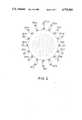
- FIG. 2is a sectional view of the plasma generating chamber having permanent magnets radially aligned at the periphery.
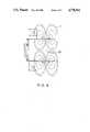
- FIG. 3is a cutaway view of the plasma generating chamber showing the magnetic flux lines of the magnetic coil.
- FIG. 4is a cutaway view of the plasma generating chamber showing the magnetic flux lines of the permanent magnets.
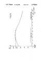
- FIG. 5is a chart of the magnetic field intensity along the central axis of the plasma generating chamber.
- FIG. 6is an exploded view of the water cooled window apparatus.
- FIG. 7is a cutaway view of the ECR plasma source configured as an ion stream source and showing the Microwave source in block diagram format.
- FIG. 8is a cutaway view of the ECR plasma source configured for ion implantation.
- FIG. 1shows a preferred embodiment of the ECR source 10 configured to emit an Ion beam, I, onto a target, T.
- a microwave beam, M, emitted from a Microwave source 12enters a plasma generating chamber 14 through a window 16.
- the plasma generating chamber 14is shaped as a cylinder as shown in the partial sectional view of FIG. 2, although other shapes may be utilized.
- the gasis introduced into the chamber 14 at channel 17.
- the gasis ionized by the microwave energy of beam M coupled with the magnetic field energy of a magnetic field formed by a first magnetic field source 18.
- the first magnetic field source 18is an electromagnetic coil which forms a band around the plasma generating chamber 14.
- the coil 18can be moved longitudinally along the axis of chamber 14 to adjust the axial location of the maximum point of the magnetic field. The maximum point occurs along the axis of the chamber at the midpoint of the coil 18.
- Other magnetic field sourcescapable of generating a sufficient magnetic field strength to achieve an ECR condition also may be used.
- the magnetic fieldcauses the electrons to orbit along the magnetic field lines while the Microwave beam energizes the electrons as the electrons orbit.
- the coupling of the microwave beam and magnetic fieldcauses the gas to form a plasma of electrons, ions, free radicals, and neutral atoms.
- ECRElectron Cyclotron Resonance
- FIG. 1depicts an ECR plasma source configured for ion beam extraction.
- the ion beam, Istrikes a target, T, on a target support 24.
- the ion beam, Iis extracted by grids 22 typically made of molybdenum and high density graphite, although the grids may be made of any conductive material that can withstand the temperature extremes of chamber 14 and have proper mechanical characteristics to avoid buckling.
- grids 22typically made of molybdenum and high density graphite, although the grids may be made of any conductive material that can withstand the temperature extremes of chamber 14 and have proper mechanical characteristics to avoid buckling.
- chamber 14will undergo a temperature change from room temperature up to 500° C. to 1,000° C.
- the molybdenum and graphite gridscan tolerate temperatures up to 2,000° C. to 3,000° C.
- the plasma formed by the electromagnetic coils 18typically concentrates ions at the center of the plasma generating chamber 14 in the plane of the coils 18. This is where the magnetic field from the coils is strongest. The plasma, if subject only to the magnetic field of the coils, would be nonuniform.
- a second magnetic field source 20is provided at the periphery of the plasma generating chamber between the first magnetic field source 18 and the extraction system 22.
- the second magnetic field source 20provides a uniform field region in the plasma generating chamber.
- the uniform field regionoccurs at the plane defined by the second magnetic field source 20.
- the magnetic field at the extraction systembe minimal so that the plasma and the ion beam output will be less magnetized and preferably unmagnetized.
- the configuration of the second magnetic field sourcealso is for reducing the net magnetic field to reduce the magnetization of the plasma.
- the second magnetic circuitis made up of a group of permanent magnets. Sixteen permanent magnets 20a-20q are illustrated in FIG. 2 although the number may vary. Although illustrated as permanent magnets 20a-20q, the second magnetic field source 20 may be any other magnetic field sources for providing a uniform and reduced field region without disrupting the ECR condition in chamber 14.
- FIG. 3illustrates the magnetic flux density produced from coils 18.
- the flux densityis shown to be highest at the midpoint of the coil along the axis of the chamber 14 as depicted by the spacing of the flux lines, F.
- the flux densitydecreases along the axis away from the midpoint of the coil 18.
- the field strength and position of the second magnetic field source 20is selected to tune the source 10.
- the objectiveis to achieve a uniform and unmagnetized (or less magnetized) ion beam output.
- the objectiveis to achieve a uniform plasma stream output.
- the field strength of the permanent magnets at the walls of chamber 14should equal the difference between the field strength of the coils 18 at the axis and the field strength of the coils at the wall of the chamber 14 in the plane of the second magnetic field source.
- FIG. 4illustrates the magnetic flux density produced from the permanent magnets 20.
- the numeral 28designates a reduced field region where magnetic fields from the permanent magnets nearly or optimally cancel out. As shown in FIG.
- the magnetic field intensity at the center of the chamber 14results primarily from the magnetic field of the first magnetic field source 18.
- the magnetic field intensity along the axisdecreases away from the coil 18.
- the magnetic field from the first magnetic sourcedecreases from the central axis toward the chamber 14 walls.
- the permanent magnets 20 a-qprovide a magnetic field which is strongest at the periphery of the chamber 14 and decreases toward the axis of the chamber.
- the coils 18provide a field which is strongest at the axis of the chamber and decreases toward the periphery of the chamber.
- the combined effect of the two magnetic fields in the plane of the permanent magnets 20is a more uniform magnetic field.
- a more uniform magnetic fieldresults in a more uniformly distributed population of ions (ion density) in the plane of the magnets 20.
- This planeis located near the extraction system. As the plasma moves out of the plane toward the extraction system 22, the plasma fans out due to the decrease in magnetic field intensity along the axis of chamber 14.
- the resulting shape of the plasma from the first and second magnetic field sources 18, 20is shown generally in FIG. 1.
- the plasmaIn the plane of the first magnetic field source 18 the plasma is compressed. As the plane moves from the coils toward the extraction system 22 the magnetic field intensity from the first magnetic field source 18 decreases, the plasma spreads out, and the magnetization of the plasma decreases.
- the second magnetic fieldis pre-adjusted to optimize the efficiency of the plasma source to provide a uniform, and for beam extraction, an unmagnetized output.
- Different intensities of the second magnetic fieldcan be designed.
- Different radial spacing(and thus number of permanent magnets--see FIG. 2) can be designed. For example, by decreasing the radial spacing the number of magnets at the periphery of chamber 14 would be increased.
- different longitudinal positioning between the first magnetic field source 18 and the extraction system 22can be designed.
- the permanent magnets 20are movable at the periphery of the chamber 14 in a longitudinal direction following the axis of the chamber 14.
- the magnetic pole configuration of the permanent magnetsmay vary.
- the design variablesthus, are magnetic field strength, radial spacing, longitudinal spacing and pole orientation.
- the plasma generating chamber 14operates at a high potential handling power inputs typically of the order of 500 to 1,000 Watts.
- a shield 26is included to isolate the chamber 14 from the external environment at the periphery of the chamber 14.
- the microwave source 12is positioned at one end of the chamber 14 and does not need to operate at a high potential. By providing a voltage isolator between the Microwave source 12 and the chamber 14, the Microwave source 12 may be operated at or near ground potential while the plasma generating chamber 14 operates at a high potential.
- the voltage isolatoris a window apparatus made up of two barriers 40, 42.
- the barriersare a choke flange 40 and a mating flange 42, although other types of barriers may be used.
- the choke flange 40is in contact with the Microwave circuitry while the mating flange 42 is in contact the plasma generating chamber 14.
- the space between the two barriers 40, 42is spanned by a nonconductive window 16 and bolts 56.
- the bolts 56are arranged circumferentially around the window 16.
- the boltsare encased with an isolating material to preclude a current path from the mating flange 42 to the choke flange 40.
- the spacing between the barriers 40, 42need only be enough to prevent a voltage jump between the mating flange 42 which is at a high potential and the choke flange 40 which is at or near ground potential.
- the isolationis operable for approximately a 10,000 volt differential.
- the window 16is made of fused quartz, although other nonconductive materials transparent at microwave frequencies also may be used.
- Fused quartzhas a dc conductivity at room temperature of 2 ⁇ 10 -17 (ohm-m) -1 .
- the dielectric constant of fused quartz at (10 w)/(2 pi)GHzis 3.78.
- the window 16will absorb heat to such an extent that it may be a limiting factor on the energy level at which the ECR source 10 can operate. To avoid this problem the heat is transferred from the window 16 by conductive cooling. Water flows through the choke flange 40 in channel 44 and through the mating flange 42 in channel 46. By conductive heat transfer from window 16 to the flanges 40, 42, then to the water flowing through the channels 44, 46 the window 16 is cooled.
- the window apparatusalso is a pressure isolator which keeps the plasma generating chamber at a vacuum pressure of approximately 10 -4 Torr while the microwave source 12 operates at or near atmospheric pressure.
- Vacuum seals 50 and 52are provided to seal the plasma generating chamber 14 at the window 16.
- the seals 50 and 52are metal annular rings which fit within the respective annular recesses of the flanges 40, 42. Metal is used so that the vacuum seals are compatible with the reactive gases used in the RIE, RIBE, CAIBE and RISE applications. Other compatible materials, however, may be used in these applications. Conventional rubber seals may be used in the nonreactive gas applications.
- the window apparatusalso includes a microwave choke for reducing the microwave leakage while entering the plasma generating chamber 14.
- the microwave chokeis a conventional choke built into the choke flange 40.
- FIG. 1illustrates an Ion beam extraction configuration.
- the use of the word beamreflecrs the use of a grid set as the extraction system 22 to accelerate the ions.
- Such an embodimentis used for Chemically Assisted Reactive Ion Beam Etching (CAIBE) and Reactive Ion Beam Etching (RIBE).
- CAIBEChemically Assisted Reactive Ion Beam Etching
- RIBEReactive Ion Beam Etching
- FIG. 7illustrates a plasma extraction configuration.
- the extraction systemincludes an orifice through which the plasma streams.
- a gas jet 60is included for introducing gas into the target chamber.
- Such a configurationwould be used for deposition processes and Reactive Ion Stream Etching (RISE), although other non beam applications might also be accomplished.
- RISEReactive Ion Stream Etching
- FIG. 8illustrates an ion implantation configuration.
- the ionspass through optics 62 into a mass selection device 64.
- the ionsare then accelerated by a accelerator 66 and pass through a scan device 68, before impacting the target, T.
Landscapes
- Chemical & Material Sciences (AREA)
- Engineering & Computer Science (AREA)
- Combustion & Propulsion (AREA)
- Analytical Chemistry (AREA)
- Electron Sources, Ion Sources (AREA)
- Plasma Technology (AREA)
- Physical Vapour Deposition (AREA)
- Drying Of Semiconductors (AREA)
Abstract
Description
f.sub.m =f.sub.ECR =(2.80×10.sup.6) B H.sub.z
Claims (24)
Priority Applications (4)
| Application Number | Priority Date | Filing Date | Title |
|---|---|---|---|
| US07/115,433US4778561A (en) | 1987-10-30 | 1987-10-30 | Electron cyclotron resonance plasma source |
| EP19880908819EP0344236A4 (en) | 1987-10-30 | 1988-08-17 | Electron cyclotron resonance plasma source |
| PCT/US1988/002823WO1989004217A1 (en) | 1987-10-30 | 1988-08-17 | Electron cyclotron resonance plasma source |
| JP63507979AJPH02501965A (en) | 1987-10-30 | 1988-08-17 | Electron cyclotron resonance plasma source |
Applications Claiming Priority (1)
| Application Number | Priority Date | Filing Date | Title |
|---|---|---|---|
| US07/115,433US4778561A (en) | 1987-10-30 | 1987-10-30 | Electron cyclotron resonance plasma source |
Publications (1)
| Publication Number | Publication Date |
|---|---|
| US4778561Atrue US4778561A (en) | 1988-10-18 |
Family
ID=22361375
Family Applications (1)
| Application Number | Title | Priority Date | Filing Date |
|---|---|---|---|
| US07/115,433Expired - LifetimeUS4778561A (en) | 1987-10-30 | 1987-10-30 | Electron cyclotron resonance plasma source |
Country Status (4)
| Country | Link |
|---|---|
| US (1) | US4778561A (en) |
| EP (1) | EP0344236A4 (en) |
| JP (1) | JPH02501965A (en) |
| WO (1) | WO1989004217A1 (en) |
Cited By (108)
| Publication number | Priority date | Publication date | Assignee | Title |
|---|---|---|---|---|
| US4854266A (en)* | 1987-11-02 | 1989-08-08 | Btu Engineering Corporation | Cross-flow diffusion furnace |
| US4877509A (en)* | 1988-07-05 | 1989-10-31 | Mitsubishi Denki Kabushiki Kaisha | Semiconductor wafer treating apparatus utilizing a plasma |
| US4883686A (en)* | 1988-05-26 | 1989-11-28 | Energy Conversion Devices, Inc. | Method for the high rate plasma deposition of high quality material |
| US4906900A (en)* | 1989-04-03 | 1990-03-06 | Board Of Trustees Operating Michigan State University | Coaxial cavity type, radiofrequency wave, plasma generating apparatus |
| DE3903322A1 (en)* | 1989-02-04 | 1990-08-16 | Nmi Naturwissenschaftl U Mediz | Method for producing ions |
| US4952273A (en)* | 1988-09-21 | 1990-08-28 | Microscience, Inc. | Plasma generation in electron cyclotron resonance |
| WO1990010547A1 (en)* | 1989-03-09 | 1990-09-20 | Applied Microwave Plasma Concepts, Inc. | Electron cyclotron resonance plasma source and method of operation |
| US4962063A (en)* | 1988-11-10 | 1990-10-09 | Applied Materials, Inc. | Multistep planarized chemical vapor deposition process with the use of low melting inorganic material for flowing while depositing |
| US4973883A (en)* | 1987-05-01 | 1990-11-27 | Semiconductor Energy Laborator Co., Ltd. | Plasma processing apparatus with a lisitano coil |
| US4977352A (en)* | 1988-06-24 | 1990-12-11 | Hughes Aircraft Company | Plasma generator having rf driven cathode |
| US5003152A (en)* | 1987-04-27 | 1991-03-26 | Nippon Telegraph And Telephone Corporation | Microwave transforming method and plasma processing |
| US5021919A (en)* | 1988-10-14 | 1991-06-04 | Leybold Aktiengesellschaft | Device for the generation of electrically charged and/or uncharged particles |
| US5032202A (en)* | 1989-10-03 | 1991-07-16 | Martin Marietta Energy Systems, Inc. | Plasma generating apparatus for large area plasma processing |
| US5032205A (en)* | 1989-05-05 | 1991-07-16 | Wisconsin Alumni Research Foundation | Plasma etching apparatus with surface magnetic fields |
| US5034086A (en)* | 1988-01-20 | 1991-07-23 | Canon Kabushiki Kaisha | Plasma processing apparatus for etching, ashing and film-formation |
| US5045166A (en)* | 1990-05-21 | 1991-09-03 | Mcnc | Magnetron method and apparatus for producing high density ionic gas discharge |
| DE4107753A1 (en)* | 1990-03-12 | 1991-09-19 | Fuji Electric Co Ltd | PLASMA PROCESSING DEVICE |
| US5115167A (en)* | 1988-04-05 | 1992-05-19 | Mitsubishi Denki Kabushiki Kaisha | Plasma processor |
| US5133830A (en)* | 1989-04-07 | 1992-07-28 | Seiko Epson Corporation | Method of pretreatment and anisotropic dry etching of thin film semiconductors |
| US5133825A (en)* | 1987-04-08 | 1992-07-28 | Hi Tachi, Ltd. | Plasma generating apparatus |
| US5134965A (en)* | 1989-06-16 | 1992-08-04 | Hitachi, Ltd. | Processing apparatus and method for plasma processing |
| US5146138A (en)* | 1988-04-05 | 1992-09-08 | Mitsubishi Denki Kabushiki Kaisha | Plasma processor |
| US5145554A (en)* | 1989-02-23 | 1992-09-08 | Seiko Epson Corporation | Method of anisotropic dry etching of thin film semiconductors |
| US5162633A (en)* | 1988-06-29 | 1992-11-10 | Hitachi, Ltd. | Microwave-excited plasma processing apparatus |
| DE4119362A1 (en)* | 1991-06-12 | 1992-12-17 | Leybold Ag | PARTICLE SOURCE, ESPECIALLY FOR REACTIVE ION NETWORK AND PLASMA SUPPORTED CVD PROCESSES |
| US5194119A (en)* | 1989-05-15 | 1993-03-16 | Seiko Epson Corporation | Method of anisotropic dry etching of thin film semiconductors |
| US5203959A (en)* | 1987-04-27 | 1993-04-20 | Semiconductor Energy Laboratory Co., Ltd. | Microwave plasma etching and deposition method employing first and second magnetic fields |
| US5236537A (en)* | 1989-04-07 | 1993-08-17 | Seiko Epson Corporation | Plasma etching apparatus |
| US5266146A (en)* | 1990-09-20 | 1993-11-30 | Hitachi, Ltd. | Microwave-powered plasma-generating apparatus and method |
| US5280219A (en)* | 1991-05-21 | 1994-01-18 | Materials Research Corporation | Cluster tool soft etch module and ECR plasma generator therefor |
| US5284544A (en)* | 1990-02-23 | 1994-02-08 | Hitachi, Ltd. | Apparatus for and method of surface treatment for microelectronic devices |
| US5306985A (en)* | 1992-07-17 | 1994-04-26 | Sematech, Inc. | ECR apparatus with magnetic coil for plasma refractive index control |
| US5423945A (en)* | 1992-09-08 | 1995-06-13 | Applied Materials, Inc. | Selectivity for etching an oxide over a nitride |
| US5506475A (en)* | 1994-03-22 | 1996-04-09 | Martin Marietta Energy Systems, Inc. | Microwave electron cyclotron electron resonance (ECR) ion source with a large, uniformly distributed, axially symmetric, ECR plasma volume |
| US5508208A (en)* | 1993-09-30 | 1996-04-16 | Sony Corporation | Method of manufacturing diamond semiconductor |
| US5628883A (en)* | 1991-06-18 | 1997-05-13 | Japan Vilene Co. Ltd. | Method for generating and activating plasma process of treatment using same, and apparatus therefor |
| EP0777267A1 (en) | 1995-11-28 | 1997-06-04 | Applied Materials, Inc. | Oxide etch process with high selectivity to nitride suitable for use on surfaces of uneven topography |
| US5645645A (en)* | 1995-04-07 | 1997-07-08 | Board Of Trustees Operating Michigan State University | Method and apparatus for plasma treatment of a surface |
| US5858259A (en)* | 1987-04-27 | 1999-01-12 | Semiconductor Energy Laboratory Co., Ltd. | Plasma processing apparatus and method |
| US5969470A (en)* | 1996-11-08 | 1999-10-19 | Veeco Instruments, Inc. | Charged particle source |
| WO1999034396A3 (en)* | 1997-12-24 | 1999-11-11 | Karlsruhe Forschzent | Installation with an electron-cyclotron resonance ion source for doping stents with radioactive and non-radioactive atoms |
| US6171974B1 (en) | 1991-06-27 | 2001-01-09 | Applied Materials, Inc. | High selectivity oxide etch process for integrated circuit structures |
| US6194325B1 (en) | 1992-09-08 | 2001-02-27 | Applied Materials Inc. | Oxide etch process with high selectivity to nitride suitable for use on surfaces of uneven topography |
| US6238582B1 (en) | 1999-03-30 | 2001-05-29 | Veeco Instruments, Inc. | Reactive ion beam etching method and a thin film head fabricated using the method |
| US20020000423A1 (en)* | 1992-06-15 | 2002-01-03 | Micron Technologies, Inc. | Method for enhancing oxide to nitride selectivity through the use of independent heat control |
| US6348126B1 (en) | 2000-08-11 | 2002-02-19 | Applied Materials, Inc. | Externally excited torroidal plasma source |
| US6410449B1 (en) | 2000-08-11 | 2002-06-25 | Applied Materials, Inc. | Method of processing a workpiece using an externally excited torroidal plasma source |
| US6418874B1 (en) | 2000-05-25 | 2002-07-16 | Applied Materials, Inc. | Toroidal plasma source for plasma processing |
| US6453842B1 (en) | 2000-08-11 | 2002-09-24 | Applied Materials Inc. | Externally excited torroidal plasma source using a gas distribution plate |
| US6464891B1 (en) | 1999-03-17 | 2002-10-15 | Veeco Instruments, Inc. | Method for repetitive ion beam processing with a carbon containing ion beam |
| US6468388B1 (en) | 2000-08-11 | 2002-10-22 | Applied Materials, Inc. | Reactor chamber for an externally excited torroidal plasma source with a gas distribution plate |
| US6494986B1 (en) | 2000-08-11 | 2002-12-17 | Applied Materials, Inc. | Externally excited multiple torroidal plasma source |
| US20030047449A1 (en)* | 2000-08-11 | 2003-03-13 | Applied Materials, Inc. | Method to drive spatially separate resonant structure with spatially distinct plasma secondaries using a single generator and switching elements |
| US6551446B1 (en) | 2000-08-11 | 2003-04-22 | Applied Materials Inc. | Externally excited torroidal plasma source with a gas distribution plate |
| US20030185967A1 (en)* | 2002-03-27 | 2003-10-02 | Eby Raymond K. | Method and apparatus for aligning patterns on a substrate |
| US6634313B2 (en) | 2001-02-13 | 2003-10-21 | Applied Materials, Inc. | High-frequency electrostatically shielded toroidal plasma and radical source |
| US6661165B2 (en)* | 2000-11-24 | 2003-12-09 | Astrium Gmbh | Inductively coupled high-frequency electron source with a reduced power requirement as a result of an electrostatic inclusion of electrons |
| US20030226641A1 (en)* | 2000-08-11 | 2003-12-11 | Applied Materials, Inc. | Externally excited torroidal plasma source with magnetic control of ion distribution |
| US6679981B1 (en) | 2000-05-11 | 2004-01-20 | Applied Materials, Inc. | Inductive plasma loop enhancing magnetron sputtering |
| US20040089233A1 (en)* | 2002-04-11 | 2004-05-13 | Carpenter Craig M. | Deposition methods utilizing microwave excitation |
| US20040149218A1 (en)* | 2000-08-11 | 2004-08-05 | Applied Materials, Inc. | Plasma immersion ion implantation process using a capacitively coupled plasma source having low dissociation and low minimum plasma voltage |
| US20040195972A1 (en)* | 2003-04-03 | 2004-10-07 | Cornelius Wayne D. | Plasma generator useful for ion beam generation |
| US20040237897A1 (en)* | 2003-05-27 | 2004-12-02 | Hiroji Hanawa | High-Frequency electrostatically shielded toroidal plasma and radical source |
| US20040255867A1 (en)* | 2001-11-17 | 2004-12-23 | Sven Ulrich | System for generating a local electron-cyclotron microwave low-pressure plasma at a predetermined location within a processing chamber |
| US20040261720A1 (en)* | 2003-06-24 | 2004-12-30 | Tolmachev Yuri Nikolaevich | High-density plasma processing apparatus |
| KR100457497B1 (en)* | 1997-05-21 | 2005-02-05 | 삼성전자주식회사 | Edge cover apparatus of plasma process apparatus to eliminate tri-layer particles formed on substrate |
| US20050098107A1 (en)* | 2003-09-24 | 2005-05-12 | Du Bois Dale R. | Thermal processing system with cross-flow liner |
| US6893907B2 (en) | 2002-06-05 | 2005-05-17 | Applied Materials, Inc. | Fabrication of silicon-on-insulator structure using plasma immersion ion implantation |
| US20050224181A1 (en)* | 2004-04-08 | 2005-10-13 | Applied Materials, Inc. | Method and apparatus for in-situ film stack processing |
| US7094316B1 (en) | 2000-08-11 | 2006-08-22 | Applied Materials, Inc. | Externally excited torroidal plasma source |
| US7094670B2 (en) | 2000-08-11 | 2006-08-22 | Applied Materials, Inc. | Plasma immersion ion implantation process |
| US7109098B1 (en) | 2005-05-17 | 2006-09-19 | Applied Materials, Inc. | Semiconductor junction formation process including low temperature plasma deposition of an optical absorption layer and high speed optical annealing |
| US7137354B2 (en) | 2000-08-11 | 2006-11-21 | Applied Materials, Inc. | Plasma immersion ion implantation apparatus including a plasma source having low dissociation and low minimum plasma voltage |
| US7166524B2 (en) | 2000-08-11 | 2007-01-23 | Applied Materials, Inc. | Method for ion implanting insulator material to reduce dielectric constant |
| US7183177B2 (en) | 2000-08-11 | 2007-02-27 | Applied Materials, Inc. | Silicon-on-insulator wafer transfer method using surface activation plasma immersion ion implantation for wafer-to-wafer adhesion enhancement |
| US7223676B2 (en) | 2002-06-05 | 2007-05-29 | Applied Materials, Inc. | Very low temperature CVD process with independently variable conformality, stress and composition of the CVD layer |
| US7244474B2 (en) | 2004-03-26 | 2007-07-17 | Applied Materials, Inc. | Chemical vapor deposition plasma process using an ion shower grid |
| US7288491B2 (en) | 2000-08-11 | 2007-10-30 | Applied Materials, Inc. | Plasma immersion ion implantation process |
| US7291360B2 (en) | 2004-03-26 | 2007-11-06 | Applied Materials, Inc. | Chemical vapor deposition plasma process using plural ion shower grids |
| US7294563B2 (en) | 2000-08-10 | 2007-11-13 | Applied Materials, Inc. | Semiconductor on insulator vertical transistor fabrication and doping process |
| US7303982B2 (en) | 2000-08-11 | 2007-12-04 | Applied Materials, Inc. | Plasma immersion ion implantation process using an inductively coupled plasma source having low dissociation and low minimum plasma voltage |
| US7312148B2 (en) | 2005-08-08 | 2007-12-25 | Applied Materials, Inc. | Copper barrier reflow process employing high speed optical annealing |
| US7312162B2 (en) | 2005-05-17 | 2007-12-25 | Applied Materials, Inc. | Low temperature plasma deposition process for carbon layer deposition |
| US7320734B2 (en) | 2000-08-11 | 2008-01-22 | Applied Materials, Inc. | Plasma immersion ion implantation system including a plasma source having low dissociation and low minimum plasma voltage |
| US7323401B2 (en) | 2005-08-08 | 2008-01-29 | Applied Materials, Inc. | Semiconductor substrate process using a low temperature deposited carbon-containing hard mask |
| US7335611B2 (en) | 2005-08-08 | 2008-02-26 | Applied Materials, Inc. | Copper conductor annealing process employing high speed optical annealing with a low temperature-deposited optical absorber layer |
| US7422775B2 (en) | 2005-05-17 | 2008-09-09 | Applied Materials, Inc. | Process for low temperature plasma deposition of an optical absorption layer and high speed optical annealing |
| US7429532B2 (en) | 2005-08-08 | 2008-09-30 | Applied Materials, Inc. | Semiconductor substrate process using an optically writable carbon-containing mask |
| US7428915B2 (en) | 2005-04-26 | 2008-09-30 | Applied Materials, Inc. | O-ringless tandem throttle valve for a plasma reactor chamber |
| US7465478B2 (en) | 2000-08-11 | 2008-12-16 | Applied Materials, Inc. | Plasma immersion ion implantation process |
| US7479456B2 (en) | 2004-08-26 | 2009-01-20 | Applied Materials, Inc. | Gasless high voltage high contact force wafer contact-cooling electrostatic chuck |
| US7666464B2 (en) | 2004-10-23 | 2010-02-23 | Applied Materials, Inc. | RF measurement feedback control and diagnostics for a plasma immersion ion implantation reactor |
| US7695590B2 (en) | 2004-03-26 | 2010-04-13 | Applied Materials, Inc. | Chemical vapor deposition plasma reactor having plural ion shower grids |
| US20100174245A1 (en)* | 2009-01-08 | 2010-07-08 | Ward Dean Halverson | System for pretreating the lumen of a catheter |
| US7767561B2 (en) | 2004-07-20 | 2010-08-03 | Applied Materials, Inc. | Plasma immersion ion implantation reactor having an ion shower grid |
| US20100289409A1 (en)* | 2009-05-15 | 2010-11-18 | Rosenthal Glenn B | Particle beam source apparatus, system and method |
| US8058156B2 (en)* | 2004-07-20 | 2011-11-15 | Applied Materials, Inc. | Plasma immersion ion implantation reactor having multiple ion shower grids |
| US20130001196A1 (en)* | 2011-06-30 | 2013-01-03 | Hoffman Daniel J | Projected Plasma Source |
| EP2551890A1 (en)* | 2011-07-29 | 2013-01-30 | Valeo Vision | System and method of treating an object by a plasma generator |
| US20130302999A1 (en)* | 2012-05-10 | 2013-11-14 | Tae Kyung Won | Siox process chemistry development using microwave plasma cvd |
| CN103996591A (en)* | 2013-02-18 | 2014-08-20 | 住友重机械工业株式会社 | Microwave ion source and method for starting same |
| US20140238301A1 (en)* | 2012-08-15 | 2014-08-28 | Chugai Ro Co., Ltd. | Plasma processing apparatus |
| US8962224B2 (en) | 2012-08-13 | 2015-02-24 | Applied Materials, Inc. | Methods for controlling defects for extreme ultraviolet lithography (EUVL) photomask substrate |
| US9039910B2 (en) | 2010-10-27 | 2015-05-26 | Applied Materials, Inc. | Methods and apparatus for controlling photoresist line width roughness |
| US20160029472A1 (en)* | 2013-03-13 | 2016-01-28 | Radom Corporation | Plasma Generator Using Dielectric Resonator |
| CN108231514A (en)* | 2016-12-15 | 2018-06-29 | 台湾积体电路制造股份有限公司 | Ion implanter and method of implanting ions into semiconductor substrate |
| CN111149438A (en)* | 2017-11-24 | 2020-05-12 | 国立研究开发法人宇宙航空研究开发机构 | microwave plasma source |
| WO2024098875A1 (en)* | 2022-11-11 | 2024-05-16 | 江苏鲁汶仪器股份有限公司 | Ion source device, ion source system and debugging method therefor |
Families Citing this family (4)
| Publication number | Priority date | Publication date | Assignee | Title |
|---|---|---|---|---|
| IT1246684B (en)* | 1991-03-07 | 1994-11-24 | Proel Tecnologie Spa | CYCLOTRONIC RESONANCE IONIC PROPULSOR. |
| JP2693899B2 (en)* | 1992-10-09 | 1997-12-24 | 栄電子工業株式会社 | ECR plasma processing method |
| CN102340921A (en)* | 2010-07-16 | 2012-02-01 | 财团法人工业技术研究院 | Electron cyclotron resonance magnetic module and electron cyclotron resonance device |
| JP5656769B2 (en)* | 2011-08-08 | 2015-01-21 | 住友重機械工業株式会社 | Microwave ion source and ion generation method |
Citations (53)
| Publication number | Priority date | Publication date | Assignee | Title |
|---|---|---|---|---|
| US3212974A (en)* | 1959-06-23 | 1965-10-19 | Csf | Particle injecting device |
| US3291715A (en)* | 1963-08-19 | 1966-12-13 | Litton Systems Inc | Apparatus for cathode sputtering including a plasmaconfining chamber |
| US3330752A (en)* | 1964-12-31 | 1967-07-11 | Ibm | Method and apparatus for cathode sputtering including suppressing temperature rise adjacent the anode using a localized magnetic field |
| US3375452A (en)* | 1967-01-13 | 1968-03-26 | Atomic Energy Commission Usa | Ferrite adjustable kicker magnet for extracting beams of charged particles |
| US3390293A (en)* | 1964-06-30 | 1968-06-25 | Varian Associates | High energy particle generator |
| US3418206A (en)* | 1963-04-29 | 1968-12-24 | Boeing Co | Particle accelerator |
| US3431461A (en)* | 1962-01-22 | 1969-03-04 | Hitachi Ltd | Electron cyclotron resonance heating device |
| US3528387A (en)* | 1964-03-17 | 1970-09-15 | Singer General Precision | Ion cleaning and vapor deposition |
| US3552124A (en)* | 1968-09-09 | 1971-01-05 | Nasa | Ion thrustor accelerator system |
| US3708418A (en)* | 1970-03-05 | 1973-01-02 | Rca Corp | Apparatus for etching of thin layers of material by ion bombardment |
| US3744247A (en)* | 1971-09-14 | 1973-07-10 | Nasa | Single grid accelerator for an ion thrustor |
| US3778656A (en)* | 1971-07-29 | 1973-12-11 | Commissariat Energie Atomique | Ion source employing a microwave resonant cavity |
| US3824388A (en)* | 1972-06-26 | 1974-07-16 | J Cugini | Hydrocarbon cracking system |
| US3916034A (en)* | 1971-05-21 | 1975-10-28 | Hitachi Ltd | Method of transporting substances in a plasma stream to and depositing it on a target |
| US3937917A (en)* | 1972-03-06 | 1976-02-10 | Commissariat A L'energie Atomique | Method for producing and heating a plasma |
| US4045677A (en)* | 1976-06-11 | 1977-08-30 | Cornell Research Foundation, Inc. | Intense ion beam generator |
| US4058748A (en)* | 1976-05-13 | 1977-11-15 | Hitachi, Ltd. | Microwave discharge ion source |
| US4065369A (en)* | 1975-07-18 | 1977-12-27 | Tokyo Shibaura Electric Co., Ltd. | Activated gas reaction apparatus & method |
| US4123316A (en)* | 1975-10-06 | 1978-10-31 | Hitachi, Ltd. | Plasma processor |
| US4233109A (en)* | 1976-01-16 | 1980-11-11 | Zaidan Hojin Handotai Kenkyu Shinkokai | Dry etching method |
| US4287419A (en)* | 1978-05-22 | 1981-09-01 | The United States Of America As Represented By The United States Department Of Energy | Strong focus space charge |
| US4293794A (en)* | 1980-04-01 | 1981-10-06 | Kapetanakos Christos A | Generation of intense, high-energy ion pulses by magnetic compression of ion rings |
| US4303865A (en)* | 1978-08-25 | 1981-12-01 | Commonwealth Scientific & Industrial Research Organization | Cold cathode ion source |
| US4316090A (en)* | 1979-06-04 | 1982-02-16 | Hitachi, Ltd. | Microwave plasma ion source |
| US4356073A (en)* | 1981-02-12 | 1982-10-26 | Shatterproof Glass Corporation | Magnetron cathode sputtering apparatus |
| US4393333A (en)* | 1979-12-10 | 1983-07-12 | Hitachi, Ltd. | Microwave plasma ion source |
| US4401054A (en)* | 1980-05-02 | 1983-08-30 | Nippon Telegraph & Telephone Public Corporation | Plasma deposition apparatus |
| US4409520A (en)* | 1980-03-24 | 1983-10-11 | Hitachi, Ltd. | Microwave discharge ion source |
| US4417178A (en)* | 1980-02-13 | 1983-11-22 | Richard Geller | Process and apparatus for producing highly charged large ions and an application utilizing this process |
| US4438368A (en)* | 1980-11-05 | 1984-03-20 | Mitsubishi Denki Kabushiki Kaisha | Plasma treating apparatus |
| US4450031A (en)* | 1982-09-10 | 1984-05-22 | Nippon Telegraph & Telephone Public Corporation | Ion shower apparatus |
| US4491735A (en)* | 1982-04-05 | 1985-01-01 | The Perkin-Elmer Corporation | Restricted ion source of high current density |
| US4492620A (en)* | 1982-09-10 | 1985-01-08 | Nippon Telegraph & Telephone Public Corporation | Plasma deposition method and apparatus |
| US4516050A (en)* | 1982-07-14 | 1985-05-07 | Varian Associates, Inc. | Ion chamber for electron-bombardment ion sources |
| US4529571A (en)* | 1982-10-27 | 1985-07-16 | The United States Of America As Represented By The United States Department Of Energy | Single-ring magnetic cusp low gas pressure ion source |
| US4543465A (en)* | 1982-08-30 | 1985-09-24 | Hitachi, Ltd. | Microwave plasma source having improved switching operation from plasma ignition phase to normal ion extraction phase |
| US4553256A (en)* | 1982-12-13 | 1985-11-12 | Moses Kenneth G | Apparatus and method for plasma generation of x-ray bursts |
| US4554484A (en)* | 1983-08-29 | 1985-11-19 | The United States Of America As Represented By The Secretary Of The Navy | Complex cavity gyrotron |
| US4580120A (en)* | 1983-08-30 | 1986-04-01 | Commissariat A L'energie Atomique | Ferromagnetic structure of an ion source produced by permanent magnets and solenoids |
| US4581100A (en)* | 1984-10-29 | 1986-04-08 | International Business Machines Corporation | Mixed excitation plasma etching system |
| US4585668A (en)* | 1983-02-28 | 1986-04-29 | Michigan State University | Method for treating a surface with a microwave or UHF plasma and improved apparatus |
| US4598231A (en)* | 1982-11-25 | 1986-07-01 | Nissin-High Voltage Co. Ltd. | Microwave ion source |
| US4609428A (en)* | 1984-07-23 | 1986-09-02 | Fujitsu Limited | Method and apparatus for microwave plasma anisotropic dry etching |
| US4611121A (en)* | 1983-04-19 | 1986-09-09 | Nihon Shinku Gijutsu Kabushiki Kaisha | Magnet apparatus |
| US4630566A (en)* | 1984-08-16 | 1986-12-23 | Board Of Trustees Operating Michigan State University | Microwave or UHF plasma improved apparatus |
| US4631438A (en)* | 1983-12-07 | 1986-12-23 | Commissariat A L'energie Atomique | Multicharged ion source with several electron cyclotron resonance zones |
| US4636688A (en)* | 1983-09-30 | 1987-01-13 | Kabushiki Kaisha Toshiba | Gyrotron device |
| US4638209A (en)* | 1983-09-08 | 1987-01-20 | Anelva Corporation | Ion beam generating apparatus |
| US4638216A (en)* | 1983-05-20 | 1987-01-20 | Commissariat A L'energie Atomique | Electron cyclotron resonance ion source |
| US4642571A (en)* | 1984-07-18 | 1987-02-10 | Tokyo Institute Of Technology | Microwave pulse source |
| US4659899A (en)* | 1984-10-24 | 1987-04-21 | The Perkin-Elmer Corporation | Vacuum-compatible air-cooled plasma device |
| US4661783A (en)* | 1981-03-18 | 1987-04-28 | The United States Of America As Represented By The Secretary Of The Navy | Free electron and cyclotron resonance distributed feedback lasers and masers |
| US4664747A (en)* | 1985-03-28 | 1987-05-12 | Anelva Corporation | Surface processing apparatus utilizing local thermal equilibrium plasma and method of using same |
Family Cites Families (2)
| Publication number | Priority date | Publication date | Assignee | Title |
|---|---|---|---|---|
| JPH0616384B2 (en)* | 1984-06-11 | 1994-03-02 | 日本電信電話株式会社 | Microwave ion source |
| JPH0654644B2 (en)* | 1985-10-04 | 1994-07-20 | 株式会社日立製作所 | Ion source |
- 1987
- 1987-10-30USUS07/115,433patent/US4778561A/ennot_activeExpired - Lifetime
- 1988
- 1988-08-17EPEP19880908819patent/EP0344236A4/ennot_activeWithdrawn
- 1988-08-17WOPCT/US1988/002823patent/WO1989004217A1/ennot_activeApplication Discontinuation
- 1988-08-17JPJP63507979Apatent/JPH02501965A/enactivePending
Patent Citations (53)
| Publication number | Priority date | Publication date | Assignee | Title |
|---|---|---|---|---|
| US3212974A (en)* | 1959-06-23 | 1965-10-19 | Csf | Particle injecting device |
| US3431461A (en)* | 1962-01-22 | 1969-03-04 | Hitachi Ltd | Electron cyclotron resonance heating device |
| US3418206A (en)* | 1963-04-29 | 1968-12-24 | Boeing Co | Particle accelerator |
| US3291715A (en)* | 1963-08-19 | 1966-12-13 | Litton Systems Inc | Apparatus for cathode sputtering including a plasmaconfining chamber |
| US3528387A (en)* | 1964-03-17 | 1970-09-15 | Singer General Precision | Ion cleaning and vapor deposition |
| US3390293A (en)* | 1964-06-30 | 1968-06-25 | Varian Associates | High energy particle generator |
| US3330752A (en)* | 1964-12-31 | 1967-07-11 | Ibm | Method and apparatus for cathode sputtering including suppressing temperature rise adjacent the anode using a localized magnetic field |
| US3375452A (en)* | 1967-01-13 | 1968-03-26 | Atomic Energy Commission Usa | Ferrite adjustable kicker magnet for extracting beams of charged particles |
| US3552124A (en)* | 1968-09-09 | 1971-01-05 | Nasa | Ion thrustor accelerator system |
| US3708418A (en)* | 1970-03-05 | 1973-01-02 | Rca Corp | Apparatus for etching of thin layers of material by ion bombardment |
| US3916034A (en)* | 1971-05-21 | 1975-10-28 | Hitachi Ltd | Method of transporting substances in a plasma stream to and depositing it on a target |
| US3778656A (en)* | 1971-07-29 | 1973-12-11 | Commissariat Energie Atomique | Ion source employing a microwave resonant cavity |
| US3744247A (en)* | 1971-09-14 | 1973-07-10 | Nasa | Single grid accelerator for an ion thrustor |
| US3937917A (en)* | 1972-03-06 | 1976-02-10 | Commissariat A L'energie Atomique | Method for producing and heating a plasma |
| US3824388A (en)* | 1972-06-26 | 1974-07-16 | J Cugini | Hydrocarbon cracking system |
| US4065369A (en)* | 1975-07-18 | 1977-12-27 | Tokyo Shibaura Electric Co., Ltd. | Activated gas reaction apparatus & method |
| US4123316A (en)* | 1975-10-06 | 1978-10-31 | Hitachi, Ltd. | Plasma processor |
| US4233109A (en)* | 1976-01-16 | 1980-11-11 | Zaidan Hojin Handotai Kenkyu Shinkokai | Dry etching method |
| US4058748A (en)* | 1976-05-13 | 1977-11-15 | Hitachi, Ltd. | Microwave discharge ion source |
| US4045677A (en)* | 1976-06-11 | 1977-08-30 | Cornell Research Foundation, Inc. | Intense ion beam generator |
| US4287419A (en)* | 1978-05-22 | 1981-09-01 | The United States Of America As Represented By The United States Department Of Energy | Strong focus space charge |
| US4303865A (en)* | 1978-08-25 | 1981-12-01 | Commonwealth Scientific & Industrial Research Organization | Cold cathode ion source |
| US4316090A (en)* | 1979-06-04 | 1982-02-16 | Hitachi, Ltd. | Microwave plasma ion source |
| US4393333A (en)* | 1979-12-10 | 1983-07-12 | Hitachi, Ltd. | Microwave plasma ion source |
| US4417178A (en)* | 1980-02-13 | 1983-11-22 | Richard Geller | Process and apparatus for producing highly charged large ions and an application utilizing this process |
| US4409520A (en)* | 1980-03-24 | 1983-10-11 | Hitachi, Ltd. | Microwave discharge ion source |
| US4293794A (en)* | 1980-04-01 | 1981-10-06 | Kapetanakos Christos A | Generation of intense, high-energy ion pulses by magnetic compression of ion rings |
| US4401054A (en)* | 1980-05-02 | 1983-08-30 | Nippon Telegraph & Telephone Public Corporation | Plasma deposition apparatus |
| US4438368A (en)* | 1980-11-05 | 1984-03-20 | Mitsubishi Denki Kabushiki Kaisha | Plasma treating apparatus |
| US4356073A (en)* | 1981-02-12 | 1982-10-26 | Shatterproof Glass Corporation | Magnetron cathode sputtering apparatus |
| US4661783A (en)* | 1981-03-18 | 1987-04-28 | The United States Of America As Represented By The Secretary Of The Navy | Free electron and cyclotron resonance distributed feedback lasers and masers |
| US4491735A (en)* | 1982-04-05 | 1985-01-01 | The Perkin-Elmer Corporation | Restricted ion source of high current density |
| US4516050A (en)* | 1982-07-14 | 1985-05-07 | Varian Associates, Inc. | Ion chamber for electron-bombardment ion sources |
| US4543465A (en)* | 1982-08-30 | 1985-09-24 | Hitachi, Ltd. | Microwave plasma source having improved switching operation from plasma ignition phase to normal ion extraction phase |
| US4450031A (en)* | 1982-09-10 | 1984-05-22 | Nippon Telegraph & Telephone Public Corporation | Ion shower apparatus |
| US4492620A (en)* | 1982-09-10 | 1985-01-08 | Nippon Telegraph & Telephone Public Corporation | Plasma deposition method and apparatus |
| US4529571A (en)* | 1982-10-27 | 1985-07-16 | The United States Of America As Represented By The United States Department Of Energy | Single-ring magnetic cusp low gas pressure ion source |
| US4598231A (en)* | 1982-11-25 | 1986-07-01 | Nissin-High Voltage Co. Ltd. | Microwave ion source |
| US4553256A (en)* | 1982-12-13 | 1985-11-12 | Moses Kenneth G | Apparatus and method for plasma generation of x-ray bursts |
| US4585668A (en)* | 1983-02-28 | 1986-04-29 | Michigan State University | Method for treating a surface with a microwave or UHF plasma and improved apparatus |
| US4611121A (en)* | 1983-04-19 | 1986-09-09 | Nihon Shinku Gijutsu Kabushiki Kaisha | Magnet apparatus |
| US4638216A (en)* | 1983-05-20 | 1987-01-20 | Commissariat A L'energie Atomique | Electron cyclotron resonance ion source |
| US4554484A (en)* | 1983-08-29 | 1985-11-19 | The United States Of America As Represented By The Secretary Of The Navy | Complex cavity gyrotron |
| US4580120A (en)* | 1983-08-30 | 1986-04-01 | Commissariat A L'energie Atomique | Ferromagnetic structure of an ion source produced by permanent magnets and solenoids |
| US4638209A (en)* | 1983-09-08 | 1987-01-20 | Anelva Corporation | Ion beam generating apparatus |
| US4636688A (en)* | 1983-09-30 | 1987-01-13 | Kabushiki Kaisha Toshiba | Gyrotron device |
| US4631438A (en)* | 1983-12-07 | 1986-12-23 | Commissariat A L'energie Atomique | Multicharged ion source with several electron cyclotron resonance zones |
| US4642571A (en)* | 1984-07-18 | 1987-02-10 | Tokyo Institute Of Technology | Microwave pulse source |
| US4609428A (en)* | 1984-07-23 | 1986-09-02 | Fujitsu Limited | Method and apparatus for microwave plasma anisotropic dry etching |
| US4630566A (en)* | 1984-08-16 | 1986-12-23 | Board Of Trustees Operating Michigan State University | Microwave or UHF plasma improved apparatus |
| US4659899A (en)* | 1984-10-24 | 1987-04-21 | The Perkin-Elmer Corporation | Vacuum-compatible air-cooled plasma device |
| US4581100A (en)* | 1984-10-29 | 1986-04-08 | International Business Machines Corporation | Mixed excitation plasma etching system |
| US4664747A (en)* | 1985-03-28 | 1987-05-12 | Anelva Corporation | Surface processing apparatus utilizing local thermal equilibrium plasma and method of using same |
Non-Patent Citations (28)
| Title |
|---|
| ECR 2000R product brochure by Plasma Technology discloses ECR Etching System.* |
| ECR 2000R product brochure by Plasma Technology--discloses ECR Etching System. |
| ECR 3000R product brochure by Plasma Technology discloses ECR Deposition System.* |
| ECR 3000R product brochure by Plasma Technology--discloses ECR Deposition System. |
| George R. Brewer, Ion Propulsion Technology and Applications, Gordon and Breach, Science Publishers, Inc. pp. 184 249; 1970.* |
| George R. Brewer, Ion Propulsion Technology and Applications, Gordon and Breach, Science Publishers, Inc. pp. 184-249; 1970. |
| J. F. Decker and C. V. D Amico, Cyclotron Resonance Plasma Source with Variable Temperature and Density Profiles , The Review of Scientific Instruments; vol. 41, No. 10, Oct. 1970.* |
| J. F. Decker and C. V. D'Amico, "Cyclotron Resonance Plasma Source with Variable Temperature and Density Profiles", The Review of Scientific Instruments; vol. 41, No. 10, Oct. 1970. |
| J. Musil, F. Zacek, "Anomalous Absorption of Intense Electromagnetic Waves in a Plasma at High Magnetic Fields"; Plasma Physics, vol. 16, pp. 735-739 (1974). |
| J. Musil, F. Zacek, "Effect of the Polarization of the Electromagnetic Wave on Wave Energy Absorption Caused by the Linear Transformation of Waves", Czech Journal of Physics, B 22 (1972). |
| J. Musil, F. Zacek, Anomalous Absorption of Intense Electromagnetic Waves in a Plasma at High Magnetic Fields ; Plasma Physics, vol. 16, pp. 735 739 (1974).* |
| J. Musil, F. Zacek, Effect of the Polarization of the Electromagnetic Wave on Wave Energy Absorption Caused by the Linear Transformation of Waves , Czech Journal of Physics, B 22 (1972).* |
| M. Miyamura, O. Tsukakoshi and S. Komiya, "A 26 cm Electron-Cyclotron-Resonance Ion Source for Reactive Ion Beam Etching of SiO2 Si", Journal of Vacuum Science Technology, vol. 20, No. 4, Apr. 1982. |
| M. Miyamura, O. Tsukakoshi and S. Komiya, A 26 cm Electron Cyclotron Resonance Ion Source for Reactive Ion Beam Etching of SiO 2 Si , Journal of Vacuum Science Technology, vol. 20, No. 4, Apr. 1982.* |
| N. Sakudo, K. Tokiguchi, H. Koike, I. Kanomata, "Microwave Ion Source", Review of Scientific Instruments, vol. 48, No. 7, Jul. 1977. |
| N. Sakudo, K. Tokiguchi, H. Koike, I. Kanomata, Microwave Ion Source , Review of Scientific Instruments, vol. 48, No. 7, Jul. 1977.* |
| P. A. Tulle, "Off-Resonance Microwave-Created Plasmas"; Plasma Physics, vol. 15, pp. 971-976; 1973. |
| P. A. Tulle, Off Resonance Microwave Created Plasmas ; Plasma Physics, vol. 15, pp. 971 976; 1973.* |
| R. Geller, "Electron Cyclotron Resonance Multiply Charge Ion Sources", IEEE Transactions on Nuclear Science, vol. NS-23, No. 2, Apr. 1976. |
| R. Geller, Electron Cyclotron Resonance Multiply Charge Ion Sources , IEEE Transactions on Nuclear Science, vol. NS 23, No. 2, Apr. 1976.* |
| Tsutomu Tsukada; "Reactive Ion Beam ECR Sources as Used in VLSI Manufacture". |
| Tsutomu Tsukada; Reactive Ion Beam ECR Sources as Used in VLSI Manufacture .* |
| V. Kopecky, J. Musil and F. Zacek, "Absorption of Microwave Energy in a Plasma Column at High Magnetic Fields"; vol. 50A, No. 4, Dec. 16, 1974. |
| V. Kopecky, J. Musil and F. Zacek, Absorption of Microwave Energy in a Plasma Column at High Magnetic Fields ; vol. 50A, No. 4, Dec. 16, 1974.* |
| Yukio Okamoto and Hajime Tamagawa, "Production of Large Area High Current Ion Beams", The Review of Scientific Instruments, vol. 43, No. 8, Aug. 1972. |
| Yukio Okamoto and Hajime Tamagawa, "Some Features of an Electron Cyclotron Resonance Plasma Produced by Means of a Lisitano-Coil", Japanese Journal of Applied Physics; vol. 11, No. 5, May 1972. |
| Yukio Okamoto and Hajime Tamagawa, Production of Large Area High Current Ion Beams , The Review of Scientific Instruments, vol. 43, No. 8, Aug. 1972.* |
| Yukio Okamoto and Hajime Tamagawa, Some Features of an Electron Cyclotron Resonance Plasma Produced by Means of a Lisitano Coil , Japanese Journal of Applied Physics; vol. 11, No. 5, May 1972.* |
Cited By (151)
| Publication number | Priority date | Publication date | Assignee | Title |
|---|---|---|---|---|
| US5133825A (en)* | 1987-04-08 | 1992-07-28 | Hi Tachi, Ltd. | Plasma generating apparatus |
| US6217661B1 (en) | 1987-04-27 | 2001-04-17 | Semiconductor Energy Laboratory Co., Ltd. | Plasma processing apparatus and method |
| US20030021910A1 (en)* | 1987-04-27 | 2003-01-30 | Semiconductor Energy Laboratory Co., Ltd. | Plasma processing apparatus and method |
| US5858259A (en)* | 1987-04-27 | 1999-01-12 | Semiconductor Energy Laboratory Co., Ltd. | Plasma processing apparatus and method |
| US6838126B2 (en) | 1987-04-27 | 2005-01-04 | Semiconductor Energy Laboratory Co., Ltd. | Method for forming I-carbon film |
| US6423383B1 (en) | 1987-04-27 | 2002-07-23 | Semiconductor Energy Laboratory Co., Ltd. | Plasma processing apparatus and method |
| US5203959A (en)* | 1987-04-27 | 1993-04-20 | Semiconductor Energy Laboratory Co., Ltd. | Microwave plasma etching and deposition method employing first and second magnetic fields |
| US5003152A (en)* | 1987-04-27 | 1991-03-26 | Nippon Telegraph And Telephone Corporation | Microwave transforming method and plasma processing |
| US4973883A (en)* | 1987-05-01 | 1990-11-27 | Semiconductor Energy Laborator Co., Ltd. | Plasma processing apparatus with a lisitano coil |
| US4854266A (en)* | 1987-11-02 | 1989-08-08 | Btu Engineering Corporation | Cross-flow diffusion furnace |
| US5034086A (en)* | 1988-01-20 | 1991-07-23 | Canon Kabushiki Kaisha | Plasma processing apparatus for etching, ashing and film-formation |
| US5115167A (en)* | 1988-04-05 | 1992-05-19 | Mitsubishi Denki Kabushiki Kaisha | Plasma processor |
| US5146138A (en)* | 1988-04-05 | 1992-09-08 | Mitsubishi Denki Kabushiki Kaisha | Plasma processor |
| US4883686A (en)* | 1988-05-26 | 1989-11-28 | Energy Conversion Devices, Inc. | Method for the high rate plasma deposition of high quality material |
| US4977352A (en)* | 1988-06-24 | 1990-12-11 | Hughes Aircraft Company | Plasma generator having rf driven cathode |
| US5162633A (en)* | 1988-06-29 | 1992-11-10 | Hitachi, Ltd. | Microwave-excited plasma processing apparatus |
| US4877509A (en)* | 1988-07-05 | 1989-10-31 | Mitsubishi Denki Kabushiki Kaisha | Semiconductor wafer treating apparatus utilizing a plasma |
| US4952273A (en)* | 1988-09-21 | 1990-08-28 | Microscience, Inc. | Plasma generation in electron cyclotron resonance |
| US5021919A (en)* | 1988-10-14 | 1991-06-04 | Leybold Aktiengesellschaft | Device for the generation of electrically charged and/or uncharged particles |
| US4962063A (en)* | 1988-11-10 | 1990-10-09 | Applied Materials, Inc. | Multistep planarized chemical vapor deposition process with the use of low melting inorganic material for flowing while depositing |
| DE3903322A1 (en)* | 1989-02-04 | 1990-08-16 | Nmi Naturwissenschaftl U Mediz | Method for producing ions |
| US5145554A (en)* | 1989-02-23 | 1992-09-08 | Seiko Epson Corporation | Method of anisotropic dry etching of thin film semiconductors |
| WO1990010547A1 (en)* | 1989-03-09 | 1990-09-20 | Applied Microwave Plasma Concepts, Inc. | Electron cyclotron resonance plasma source and method of operation |
| US5133826A (en)* | 1989-03-09 | 1992-07-28 | Applied Microwave Plasma Concepts, Inc. | Electron cyclotron resonance plasma source |
| US4906900A (en)* | 1989-04-03 | 1990-03-06 | Board Of Trustees Operating Michigan State University | Coaxial cavity type, radiofrequency wave, plasma generating apparatus |
| US5133830A (en)* | 1989-04-07 | 1992-07-28 | Seiko Epson Corporation | Method of pretreatment and anisotropic dry etching of thin film semiconductors |
| US5236537A (en)* | 1989-04-07 | 1993-08-17 | Seiko Epson Corporation | Plasma etching apparatus |
| US5032205A (en)* | 1989-05-05 | 1991-07-16 | Wisconsin Alumni Research Foundation | Plasma etching apparatus with surface magnetic fields |
| US5194119A (en)* | 1989-05-15 | 1993-03-16 | Seiko Epson Corporation | Method of anisotropic dry etching of thin film semiconductors |
| US5134965A (en)* | 1989-06-16 | 1992-08-04 | Hitachi, Ltd. | Processing apparatus and method for plasma processing |
| US5032202A (en)* | 1989-10-03 | 1991-07-16 | Martin Marietta Energy Systems, Inc. | Plasma generating apparatus for large area plasma processing |
| US5284544A (en)* | 1990-02-23 | 1994-02-08 | Hitachi, Ltd. | Apparatus for and method of surface treatment for microelectronic devices |
| DE4107753C2 (en)* | 1990-03-12 | 1998-03-19 | Fuji Electric Co Ltd | Method for operating a plasma processing device |
| DE4107753A1 (en)* | 1990-03-12 | 1991-09-19 | Fuji Electric Co Ltd | PLASMA PROCESSING DEVICE |
| US5045166A (en)* | 1990-05-21 | 1991-09-03 | Mcnc | Magnetron method and apparatus for producing high density ionic gas discharge |
| US5266146A (en)* | 1990-09-20 | 1993-11-30 | Hitachi, Ltd. | Microwave-powered plasma-generating apparatus and method |
| US5280219A (en)* | 1991-05-21 | 1994-01-18 | Materials Research Corporation | Cluster tool soft etch module and ECR plasma generator therefor |
| DE4119362A1 (en)* | 1991-06-12 | 1992-12-17 | Leybold Ag | PARTICLE SOURCE, ESPECIALLY FOR REACTIVE ION NETWORK AND PLASMA SUPPORTED CVD PROCESSES |
| US5628883A (en)* | 1991-06-18 | 1997-05-13 | Japan Vilene Co. Ltd. | Method for generating and activating plasma process of treatment using same, and apparatus therefor |
| US6171974B1 (en) | 1991-06-27 | 2001-01-09 | Applied Materials, Inc. | High selectivity oxide etch process for integrated circuit structures |
| US20020000423A1 (en)* | 1992-06-15 | 2002-01-03 | Micron Technologies, Inc. | Method for enhancing oxide to nitride selectivity through the use of independent heat control |
| US7049244B2 (en) | 1992-06-15 | 2006-05-23 | Micron Technology, Inc. | Method for enhancing silicon dioxide to silicon nitride selectivity |
| US5306985A (en)* | 1992-07-17 | 1994-04-26 | Sematech, Inc. | ECR apparatus with magnetic coil for plasma refractive index control |
| US5466991A (en)* | 1992-07-17 | 1995-11-14 | Sematech, Inc. | Optimized ECR plasma apparatus with varied microwave window thickness |
| US5423945A (en)* | 1992-09-08 | 1995-06-13 | Applied Materials, Inc. | Selectivity for etching an oxide over a nitride |
| US6194325B1 (en) | 1992-09-08 | 2001-02-27 | Applied Materials Inc. | Oxide etch process with high selectivity to nitride suitable for use on surfaces of uneven topography |
| US5508208A (en)* | 1993-09-30 | 1996-04-16 | Sony Corporation | Method of manufacturing diamond semiconductor |
| US5506475A (en)* | 1994-03-22 | 1996-04-09 | Martin Marietta Energy Systems, Inc. | Microwave electron cyclotron electron resonance (ECR) ion source with a large, uniformly distributed, axially symmetric, ECR plasma volume |
| US5645645A (en)* | 1995-04-07 | 1997-07-08 | Board Of Trustees Operating Michigan State University | Method and apparatus for plasma treatment of a surface |
| EP0777267A1 (en) | 1995-11-28 | 1997-06-04 | Applied Materials, Inc. | Oxide etch process with high selectivity to nitride suitable for use on surfaces of uneven topography |
| US5969470A (en)* | 1996-11-08 | 1999-10-19 | Veeco Instruments, Inc. | Charged particle source |
| US6150755A (en)* | 1996-11-08 | 2000-11-21 | Veeco Instruments, Inc. | Charged particle source with liquid electrode |
| KR100457497B1 (en)* | 1997-05-21 | 2005-02-05 | 삼성전자주식회사 | Edge cover apparatus of plasma process apparatus to eliminate tri-layer particles formed on substrate |
| US6495842B1 (en) | 1997-12-24 | 2002-12-17 | Forschungszentrum Karlsruhe Gmbh | Implantation of the radioactive 32P atoms |
| WO1999034396A3 (en)* | 1997-12-24 | 1999-11-11 | Karlsruhe Forschzent | Installation with an electron-cyclotron resonance ion source for doping stents with radioactive and non-radioactive atoms |
| US6464891B1 (en) | 1999-03-17 | 2002-10-15 | Veeco Instruments, Inc. | Method for repetitive ion beam processing with a carbon containing ion beam |
| US6238582B1 (en) | 1999-03-30 | 2001-05-29 | Veeco Instruments, Inc. | Reactive ion beam etching method and a thin film head fabricated using the method |
| US6679981B1 (en) | 2000-05-11 | 2004-01-20 | Applied Materials, Inc. | Inductive plasma loop enhancing magnetron sputtering |
| US6418874B1 (en) | 2000-05-25 | 2002-07-16 | Applied Materials, Inc. | Toroidal plasma source for plasma processing |
| US6712020B2 (en) | 2000-05-25 | 2004-03-30 | Applied Materials Inc. | Toroidal plasma source for plasma processing |
| US7294563B2 (en) | 2000-08-10 | 2007-11-13 | Applied Materials, Inc. | Semiconductor on insulator vertical transistor fabrication and doping process |
| US7183177B2 (en) | 2000-08-11 | 2007-02-27 | Applied Materials, Inc. | Silicon-on-insulator wafer transfer method using surface activation plasma immersion ion implantation for wafer-to-wafer adhesion enhancement |
| US6410449B1 (en) | 2000-08-11 | 2002-06-25 | Applied Materials, Inc. | Method of processing a workpiece using an externally excited torroidal plasma source |
| US7094670B2 (en) | 2000-08-11 | 2006-08-22 | Applied Materials, Inc. | Plasma immersion ion implantation process |
| US7094316B1 (en) | 2000-08-11 | 2006-08-22 | Applied Materials, Inc. | Externally excited torroidal plasma source |
| US20030226641A1 (en)* | 2000-08-11 | 2003-12-11 | Applied Materials, Inc. | Externally excited torroidal plasma source with magnetic control of ion distribution |
| US6551446B1 (en) | 2000-08-11 | 2003-04-22 | Applied Materials Inc. | Externally excited torroidal plasma source with a gas distribution plate |
| US20030047449A1 (en)* | 2000-08-11 | 2003-03-13 | Applied Materials, Inc. | Method to drive spatially separate resonant structure with spatially distinct plasma secondaries using a single generator and switching elements |
| US7430984B2 (en) | 2000-08-11 | 2008-10-07 | Applied Materials, Inc. | Method to drive spatially separate resonant structure with spatially distinct plasma secondaries using a single generator and switching elements |
| US20040149218A1 (en)* | 2000-08-11 | 2004-08-05 | Applied Materials, Inc. | Plasma immersion ion implantation process using a capacitively coupled plasma source having low dissociation and low minimum plasma voltage |
| US7320734B2 (en) | 2000-08-11 | 2008-01-22 | Applied Materials, Inc. | Plasma immersion ion implantation system including a plasma source having low dissociation and low minimum plasma voltage |
| US7303982B2 (en) | 2000-08-11 | 2007-12-04 | Applied Materials, Inc. | Plasma immersion ion implantation process using an inductively coupled plasma source having low dissociation and low minimum plasma voltage |
| US7465478B2 (en) | 2000-08-11 | 2008-12-16 | Applied Materials, Inc. | Plasma immersion ion implantation process |
| US6453842B1 (en) | 2000-08-11 | 2002-09-24 | Applied Materials Inc. | Externally excited torroidal plasma source using a gas distribution plate |
| US7291545B2 (en) | 2000-08-11 | 2007-11-06 | Applied Materials, Inc. | Plasma immersion ion implantation process using a capacitively couple plasma source having low dissociation and low minimum plasma voltage |
| US6348126B1 (en) | 2000-08-11 | 2002-02-19 | Applied Materials, Inc. | Externally excited torroidal plasma source |
| US6468388B1 (en) | 2000-08-11 | 2002-10-22 | Applied Materials, Inc. | Reactor chamber for an externally excited torroidal plasma source with a gas distribution plate |
| US7288491B2 (en) | 2000-08-11 | 2007-10-30 | Applied Materials, Inc. | Plasma immersion ion implantation process |
| US6494986B1 (en) | 2000-08-11 | 2002-12-17 | Applied Materials, Inc. | Externally excited multiple torroidal plasma source |
| US6939434B2 (en) | 2000-08-11 | 2005-09-06 | Applied Materials, Inc. | Externally excited torroidal plasma source with magnetic control of ion distribution |
| US7166524B2 (en) | 2000-08-11 | 2007-01-23 | Applied Materials, Inc. | Method for ion implanting insulator material to reduce dielectric constant |
| US7037813B2 (en) | 2000-08-11 | 2006-05-02 | Applied Materials, Inc. | Plasma immersion ion implantation process using a capacitively coupled plasma source having low dissociation and low minimum plasma voltage |
| US7137354B2 (en) | 2000-08-11 | 2006-11-21 | Applied Materials, Inc. | Plasma immersion ion implantation apparatus including a plasma source having low dissociation and low minimum plasma voltage |
| US6661165B2 (en)* | 2000-11-24 | 2003-12-09 | Astrium Gmbh | Inductively coupled high-frequency electron source with a reduced power requirement as a result of an electrostatic inclusion of electrons |
| US6634313B2 (en) | 2001-02-13 | 2003-10-21 | Applied Materials, Inc. | High-frequency electrostatically shielded toroidal plasma and radical source |
| US20040255867A1 (en)* | 2001-11-17 | 2004-12-23 | Sven Ulrich | System for generating a local electron-cyclotron microwave low-pressure plasma at a predetermined location within a processing chamber |
| US7506609B2 (en)* | 2001-11-17 | 2009-03-24 | Forschungszentrum Karlsruhe Gmbh | System for generating a local electron-cyclotron microwave low-pressure plasma at a predetermined location within a processing chamber |
| US8043652B2 (en) | 2002-03-27 | 2011-10-25 | Nanoink, Inc. | Method and apparatus for aligning patterns on a substrate |
| US20080147346A1 (en)* | 2002-03-27 | 2008-06-19 | Nanolnk, Inc. | Method and apparatus for aligning patterns on a substrate |
| US20030185967A1 (en)* | 2002-03-27 | 2003-10-02 | Eby Raymond K. | Method and apparatus for aligning patterns on a substrate |
| US7279046B2 (en) | 2002-03-27 | 2007-10-09 | Nanoink, Inc. | Method and apparatus for aligning patterns on a substrate |
| US7105208B2 (en)* | 2002-04-11 | 2006-09-12 | Micron Technology, Inc. | Methods and processes utilizing microwave excitation |
| US20040089233A1 (en)* | 2002-04-11 | 2004-05-13 | Carpenter Craig M. | Deposition methods utilizing microwave excitation |
| US7422986B2 (en) | 2002-04-11 | 2008-09-09 | Micron Technology, Inc. | Deposition methods utilizing microwave excitation |
| US6893907B2 (en) | 2002-06-05 | 2005-05-17 | Applied Materials, Inc. | Fabrication of silicon-on-insulator structure using plasma immersion ion implantation |
| US7700465B2 (en) | 2002-06-05 | 2010-04-20 | Applied Materials, Inc. | Plasma immersion ion implantation process using a plasma source having low dissociation and low minimum plasma voltage |
| US7223676B2 (en) | 2002-06-05 | 2007-05-29 | Applied Materials, Inc. | Very low temperature CVD process with independently variable conformality, stress and composition of the CVD layer |
| US7393765B2 (en) | 2002-06-05 | 2008-07-01 | Applied Materials, Inc. | Low temperature CVD process with selected stress of the CVD layer on CMOS devices |
| US6812647B2 (en) | 2003-04-03 | 2004-11-02 | Wayne D. Cornelius | Plasma generator useful for ion beam generation |
| US20040195972A1 (en)* | 2003-04-03 | 2004-10-07 | Cornelius Wayne D. | Plasma generator useful for ion beam generation |
| US20040237897A1 (en)* | 2003-05-27 | 2004-12-02 | Hiroji Hanawa | High-Frequency electrostatically shielded toroidal plasma and radical source |
| US7210424B2 (en)* | 2003-06-24 | 2007-05-01 | Samsung Electronics Co., Ltd. | High-density plasma processing apparatus |
| US20040261720A1 (en)* | 2003-06-24 | 2004-12-30 | Tolmachev Yuri Nikolaevich | High-density plasma processing apparatus |
| CN100394535C (en)* | 2003-06-24 | 2008-06-11 | 三星电子株式会社 | High Density Plasma Processing Equipment |
| US20050098107A1 (en)* | 2003-09-24 | 2005-05-12 | Du Bois Dale R. | Thermal processing system with cross-flow liner |
| US7244474B2 (en) | 2004-03-26 | 2007-07-17 | Applied Materials, Inc. | Chemical vapor deposition plasma process using an ion shower grid |
| US7695590B2 (en) | 2004-03-26 | 2010-04-13 | Applied Materials, Inc. | Chemical vapor deposition plasma reactor having plural ion shower grids |
| US7291360B2 (en) | 2004-03-26 | 2007-11-06 | Applied Materials, Inc. | Chemical vapor deposition plasma process using plural ion shower grids |
| US7358192B2 (en) | 2004-04-08 | 2008-04-15 | Applied Materials, Inc. | Method and apparatus for in-situ film stack processing |
| US20050224181A1 (en)* | 2004-04-08 | 2005-10-13 | Applied Materials, Inc. | Method and apparatus for in-situ film stack processing |
| US7767561B2 (en) | 2004-07-20 | 2010-08-03 | Applied Materials, Inc. | Plasma immersion ion implantation reactor having an ion shower grid |
| US8058156B2 (en)* | 2004-07-20 | 2011-11-15 | Applied Materials, Inc. | Plasma immersion ion implantation reactor having multiple ion shower grids |
| US7479456B2 (en) | 2004-08-26 | 2009-01-20 | Applied Materials, Inc. | Gasless high voltage high contact force wafer contact-cooling electrostatic chuck |
| US7666464B2 (en) | 2004-10-23 | 2010-02-23 | Applied Materials, Inc. | RF measurement feedback control and diagnostics for a plasma immersion ion implantation reactor |
| US7428915B2 (en) | 2005-04-26 | 2008-09-30 | Applied Materials, Inc. | O-ringless tandem throttle valve for a plasma reactor chamber |
| US7422775B2 (en) | 2005-05-17 | 2008-09-09 | Applied Materials, Inc. | Process for low temperature plasma deposition of an optical absorption layer and high speed optical annealing |
| US7109098B1 (en) | 2005-05-17 | 2006-09-19 | Applied Materials, Inc. | Semiconductor junction formation process including low temperature plasma deposition of an optical absorption layer and high speed optical annealing |
| US7312162B2 (en) | 2005-05-17 | 2007-12-25 | Applied Materials, Inc. | Low temperature plasma deposition process for carbon layer deposition |
| US7323401B2 (en) | 2005-08-08 | 2008-01-29 | Applied Materials, Inc. | Semiconductor substrate process using a low temperature deposited carbon-containing hard mask |
| US7429532B2 (en) | 2005-08-08 | 2008-09-30 | Applied Materials, Inc. | Semiconductor substrate process using an optically writable carbon-containing mask |
| US7335611B2 (en) | 2005-08-08 | 2008-02-26 | Applied Materials, Inc. | Copper conductor annealing process employing high speed optical annealing with a low temperature-deposited optical absorber layer |
| US7312148B2 (en) | 2005-08-08 | 2007-12-25 | Applied Materials, Inc. | Copper barrier reflow process employing high speed optical annealing |
| US20100174245A1 (en)* | 2009-01-08 | 2010-07-08 | Ward Dean Halverson | System for pretreating the lumen of a catheter |
| US8624502B2 (en) | 2009-05-15 | 2014-01-07 | Alpha Source Llc | Particle beam source apparatus, system and method |
| US20100289409A1 (en)* | 2009-05-15 | 2010-11-18 | Rosenthal Glenn B | Particle beam source apparatus, system and method |
| US20100290575A1 (en)* | 2009-05-15 | 2010-11-18 | Rosenthal Glenn B | Particle beam isotope generator apparatus, system and method |
| US9659736B2 (en) | 2009-05-15 | 2017-05-23 | Alpha Source, Inc. | Particle beam isotope generator apparatus, system and method |
| US9039910B2 (en) | 2010-10-27 | 2015-05-26 | Applied Materials, Inc. | Methods and apparatus for controlling photoresist line width roughness |
| US10225919B2 (en)* | 2011-06-30 | 2019-03-05 | Aes Global Holdings, Pte. Ltd | Projected plasma source |
| US20130001196A1 (en)* | 2011-06-30 | 2013-01-03 | Hoffman Daniel J | Projected Plasma Source |
| FR2978599A1 (en)* | 2011-07-29 | 2013-02-01 | Valeo Vision | INSTALLATION AND METHOD FOR PROCESSING AN OBJECT BY A PLASMA GENERATOR |
| EP2551890A1 (en)* | 2011-07-29 | 2013-01-30 | Valeo Vision | System and method of treating an object by a plasma generator |
| US8906813B2 (en)* | 2012-05-10 | 2014-12-09 | Applied Materials, Inc. | SiOx process chemistry development using microwave plasma CVD |
| US20130302999A1 (en)* | 2012-05-10 | 2013-11-14 | Tae Kyung Won | Siox process chemistry development using microwave plasma cvd |
| US8962224B2 (en) | 2012-08-13 | 2015-02-24 | Applied Materials, Inc. | Methods for controlling defects for extreme ultraviolet lithography (EUVL) photomask substrate |
| US8986458B2 (en)* | 2012-08-15 | 2015-03-24 | Chugai Ro Co., Ltd. | Plasma processing apparatus |
| US20140238301A1 (en)* | 2012-08-15 | 2014-08-28 | Chugai Ro Co., Ltd. | Plasma processing apparatus |
| CN103996591A (en)* | 2013-02-18 | 2014-08-20 | 住友重机械工业株式会社 | Microwave ion source and method for starting same |
| US20160029472A1 (en)* | 2013-03-13 | 2016-01-28 | Radom Corporation | Plasma Generator Using Dielectric Resonator |
| US9491841B2 (en)* | 2013-03-13 | 2016-11-08 | Radom Corporation | Plasma generator using dielectric resonator |
| US20170027051A1 (en)* | 2013-03-13 | 2017-01-26 | Radom Corporation | Plasma Generator Using Dielectric Resonator |
| US9706635B2 (en)* | 2013-03-13 | 2017-07-11 | Radom Corporation | Plasma generator using dielectric resonator |
| US10163609B2 (en) | 2016-12-15 | 2018-12-25 | Taiwan Semiconductor Manufacturing Co., Ltd. | Plasma generation for ion implanter |
| CN108231514A (en)* | 2016-12-15 | 2018-06-29 | 台湾积体电路制造股份有限公司 | Ion implanter and method of implanting ions into semiconductor substrate |
| TWI742208B (en)* | 2016-12-15 | 2021-10-11 | 台灣積體電路製造股份有限公司 | Ion implanter and method of implanting ion in a semiconductor substrate |
| CN108231514B (en)* | 2016-12-15 | 2021-12-03 | 台湾积体电路制造股份有限公司 | Ion implanter and method of implanting ions into semiconductor substrate |
| CN111149438A (en)* | 2017-11-24 | 2020-05-12 | 国立研究开发法人宇宙航空研究开发机构 | microwave plasma source |
| US11259397B2 (en) | 2017-11-24 | 2022-02-22 | Japan Aerospace Exploration Agency | Microwave plasma source |
| CN111149438B (en)* | 2017-11-24 | 2022-03-18 | 国立研究开发法人宇宙航空研究开发机构 | Microwave plasma source |
| WO2024098875A1 (en)* | 2022-11-11 | 2024-05-16 | 江苏鲁汶仪器股份有限公司 | Ion source device, ion source system and debugging method therefor |
| TWI881430B (en)* | 2022-11-11 | 2025-04-21 | 大陸商江蘇魯汶儀器股份有限公司 | Ion source device, ion source system and debugging method thereof |
Also Published As
| Publication number | Publication date |
|---|---|
| WO1989004217A1 (en) | 1989-05-18 |
| EP0344236A1 (en) | 1989-12-06 |
| EP0344236A4 (en) | 1991-07-10 |
| JPH02501965A (en) | 1990-06-28 |
Similar Documents
| Publication | Publication Date | Title |
|---|---|---|
| US4778561A (en) | Electron cyclotron resonance plasma source | |
| US6803585B2 (en) | Electron-cyclotron resonance type ion beam source for ion implanter | |
| US7863582B2 (en) | Ion-beam source | |
| US5763989A (en) | Closed drift ion source with improved magnetic field | |
| EP0283519B1 (en) | Ion generation apparatus, thin film formation apparatus using the ion generation apparatus, and ion source | |
| US7176469B2 (en) | Negative ion source with external RF antenna | |
| KR940010844B1 (en) | Ion Source | |
| US5032205A (en) | Plasma etching apparatus with surface magnetic fields | |
| US5216330A (en) | Ion beam gun | |
| US20020145389A1 (en) | Magnetic field for small closed-drift ion source | |
| US5266146A (en) | Microwave-powered plasma-generating apparatus and method | |
| JPH02103932A (en) | Particle source | |
| EP0740327B1 (en) | Ion beam processing apparatus | |
| US7493869B1 (en) | Very large area/volume microwave ECR plasma and ion source | |
| US6922019B2 (en) | Microwave ion source | |
| US5726412A (en) | Linear microwave source for plasma surface treatment | |
| JPH11354508A (en) | Ion beam processing equipment | |
| Sortais | Recent progress in making highly charged ion beams | |
| CA2438098C (en) | Magnetic field for small closed-drift thruster | |
| RU2246035C1 (en) | Ion engine | |
| RU2106716C1 (en) | Plant for microwave vacuum-plasma treatment of condensed media | |
| TW201824366A (en) | Ion implanter and method of implanting ion in a semiconductor substrate | |
| JP2002056786A (en) | Ion source for ion implanting equipment | |
| JPS6386864A (en) | Ion source | |
| JPS62224686A (en) | Ion source |
Legal Events
| Date | Code | Title | Description |
|---|---|---|---|
| AS | Assignment | Owner name:VEECO INSTRUMENTS, INC., TERMINAL DRIVE, PLAINVIEW Free format text:ASSIGNMENT OF ASSIGNORS INTEREST.;ASSIGNOR:GHANBARI, EBRAHIM;REEL/FRAME:004816/0192 Effective date:19871121 | |
| STCF | Information on status: patent grant | Free format text:PATENTED CASE | |
| FEPP | Fee payment procedure | Free format text:PAYOR NUMBER ASSIGNED (ORIGINAL EVENT CODE: ASPN); ENTITY STATUS OF PATENT OWNER: LARGE ENTITY | |
| REMI | Maintenance fee reminder mailed | ||
| FPAY | Fee payment | Year of fee payment:4 | |
| SULP | Surcharge for late payment | ||
| FPAY | Fee payment | Year of fee payment:8 | |
| AS | Assignment | Owner name:FLEET BANK, N.A., AS AGENT, NEW YORK Free format text:SECURITY AGREEMENT;ASSIGNORS:VEECO INSTRUMENTS, INC.;SLOAN TECHNOLOGY CORPORATION;REEL/FRAME:008153/0049 Effective date:19960731 Owner name:CHASE MANHATTAN BANK, NEW YORK Free format text:SECURITY AGREEMENT;ASSIGNORS:VEECO INSTRUMENTS, INC.;SLOAN TECHNOLOGY CORPORATION;REEL/FRAME:008153/0049 Effective date:19960731 | |
| AS | Assignment | Owner name:VEECO INSTRUMENTS, INC., NEW YORK Free format text:RELEASE OF SECURITY INTEREST;ASSIGNORS:FLEET BANK, N.A., AS AGENT THE CHASE MANHATTAN BANK;CHASE MANHATTAN BANK, THE;REEL/FRAME:009893/0132 Effective date:19990131 | |
| FPAY | Fee payment | Year of fee payment:12 |