US4778275A - Method of aligning a mask and a substrate relative to each other and arrangement for carrying out the method - Google Patents
Method of aligning a mask and a substrate relative to each other and arrangement for carrying out the methodDownload PDFInfo
- Publication number
- US4778275A US4778275AUS06/910,710US91071086AUS4778275AUS 4778275 AUS4778275 AUS 4778275AUS 91071086 AUS91071086 AUS 91071086AUS 4778275 AUS4778275 AUS 4778275A
- Authority
- US
- United States
- Prior art keywords
- substrate
- mask
- alignment
- mark
- marks
- Prior art date
- Legal status (The legal status is an assumption and is not a legal conclusion. Google has not performed a legal analysis and makes no representation as to the accuracy of the status listed.)
- Expired - Lifetime
Links
- 239000000758substrateSubstances0.000titleclaimsabstractdescription214
- 238000000034methodMethods0.000titleclaimsabstractdescription35
- 230000005855radiationEffects0.000claimsdescription44
- 230000003287optical effectEffects0.000claimsdescription38
- 238000003384imaging methodMethods0.000claimsdescription28
- 210000001747pupilAnatomy0.000claimsdescription14
- 238000001514detection methodMethods0.000claimsdescription11
- 238000011896sensitive detectionMethods0.000claimsdescription11
- 230000000737periodic effectEffects0.000claimsdescription6
- 230000006872improvementEffects0.000claimsdescription3
- 238000006073displacement reactionMethods0.000description12
- 238000004519manufacturing processMethods0.000description7
- 230000008901benefitEffects0.000description6
- 238000009792diffusion processMethods0.000description4
- 230000006870functionEffects0.000description4
- 230000008859changeEffects0.000description2
- 230000005381magnetic domainEffects0.000description2
- 230000000873masking effectEffects0.000description2
- 239000000463materialSubstances0.000description2
- 230000015654memoryEffects0.000description2
- 229940125730polarisation modulatorDrugs0.000description2
- 239000004065semiconductorSubstances0.000description2
- 230000006978adaptationEffects0.000description1
- 230000002411adverseEffects0.000description1
- 230000006399behaviorEffects0.000description1
- 230000005540biological transmissionEffects0.000description1
- 239000002131composite materialSubstances0.000description1
- 238000010276constructionMethods0.000description1
- 230000000694effectsEffects0.000description1
- 238000005516engineering processMethods0.000description1
- -1for exampleSubstances0.000description1
- 239000011521glassSubstances0.000description1
- 239000010438graniteSubstances0.000description1
- CPBQJMYROZQQJC-UHFFFAOYSA-Nhelium neonChemical compound[He].[Ne]CPBQJMYROZQQJC-UHFFFAOYSA-N0.000description1
- 238000005286illuminationMethods0.000description1
- 230000007774longtermEffects0.000description1
- QSHDDOUJBYECFT-UHFFFAOYSA-NmercuryChemical compound[Hg]QSHDDOUJBYECFT-UHFFFAOYSA-N0.000description1
- 229910052753mercuryInorganic materials0.000description1
- 238000012986modificationMethods0.000description1
- 230000004048modificationEffects0.000description1
- 230000010287polarizationEffects0.000description1
- 230000008569processEffects0.000description1
- 239000010453quartzSubstances0.000description1
- VYPSYNLAJGMNEJ-UHFFFAOYSA-Nsilicon dioxideInorganic materialsO=[Si]=OVYPSYNLAJGMNEJ-UHFFFAOYSA-N0.000description1
- 239000000126substanceSubstances0.000description1
- 239000000725suspensionSubstances0.000description1
- 239000012780transparent materialSubstances0.000description1
Images


Classifications
- G—PHYSICS
- G03—PHOTOGRAPHY; CINEMATOGRAPHY; ANALOGOUS TECHNIQUES USING WAVES OTHER THAN OPTICAL WAVES; ELECTROGRAPHY; HOLOGRAPHY
- G03F—PHOTOMECHANICAL PRODUCTION OF TEXTURED OR PATTERNED SURFACES, e.g. FOR PRINTING, FOR PROCESSING OF SEMICONDUCTOR DEVICES; MATERIALS THEREFOR; ORIGINALS THEREFOR; APPARATUS SPECIALLY ADAPTED THEREFOR
- G03F9/00—Registration or positioning of originals, masks, frames, photographic sheets or textured or patterned surfaces, e.g. automatically
- G03F9/70—Registration or positioning of originals, masks, frames, photographic sheets or textured or patterned surfaces, e.g. automatically for microlithography
- G03F9/7049—Technique, e.g. interferometric
Definitions
- the inventionrelates to a method of aligning relative to each other a mask pattern formed in a mask and a substrate on which said mask pattern is to be imaged, using alignment marks present in the mask and in the substrate, a first substrate mark being aligned relative to a first mask mark and a second substrate mark being aligned relative to the first mask mark, which alignments are effected by means of the lens system with which the mask pattern is imaged onto the substrate.
- the inventionalso relates to an arrangement for carrying out this method.
- Diffusion and masking techniquesmay also be employed in the fabrication of other structures with details of the order of magnitude of micrometers. Examples of this are structures of integrated optical systems or guiding and detection patterns of magnetic-domain memories. In the fabrication of such structure it is also necessary to align images of mask patterns very accurately relative to a substrate.
- U.S. Pat. No. 4,251,160describes an arrangement for aligning a substrate relative to a mask pattern, wherein an alignment mark in the substrate is imaged onto an alignment in the mask, outside the mask pattern to be imaged.
- the alignment marks in the substrate and in the maskare diffraction gratings. If the image of the substrate mark coincides accurately with the mask alignment mark the substrate is aligned correctly relative to the mask pattern.
- the principal element for imaging the substrate mark on the mask markis the projection-lens system or imaging system by which the mask pattern is imaged onto the substrate.
- a first substrate markis aligned relative to a first mask mark.
- the substrateis positioned correctly at the location of the first substrate mark.
- the substrateis moved in the X-direction over a distance equal to the distance between the first substrate mark and the second substrate mark and care is taken that the second substrate mark is aligned relative to the first mask mark.
- the substratemay be rotated effectively about an axis perpendicular to the substrate plane and through the center of the mask image.
- the effective rotationmay be a combination of a rotation about an axis and a displacement transverse to this axis.
- the displacement of the substrate and the substrate tableis measured by means of, for example, an interferometer system which employs the frame of the exposure apparatus or a part of this frame as its reference.
- the angular orientation of the substrateis thus related to the frame of the exposure apparatus.
- a second mask markis imaged onto the first mask mark by a separate optical system. Care is taken that lines of the image of the second mask mark which extend in the X-direction coincide with lines of the first mask mark which extend in the X-direction.
- the X-directionis the direction in which the substrate is moved during alignment of the two substrate marks relative to the first mask mark, which X-direction is referred to the frame of the exposure apparatus by the interferometer system.
- the angular orientation of the maskis also related to the frame and, consequently, the angular orientation of the mask and the substrate relative to one another is determined by this frame. This imposes stringent requirements on the stability of the frame, specifically on the thermal stability, but also on the freedom from creep of the frame. In this respect creep is to be understood to mean the continuous deformation of a material under load in the long term.
- the exposure apparatus for the repeated imaging of mask patterns in accordance with the U.S. Pat. No. 4,251,160has proved to be very suitable for use in the fabrication of integrated circuits with minimal details, or line widths, of the order of one micrometer or more.
- the increasing demand for more electronic components per unit area of the substrate, with ever even smaller dimensions of these components,has lead to a growing need for an apparatus which is capable of repeatedly making images whose details or line widths are smaller than one micrometer.
- the projection-lens system or imaging system for such an apparatus by means of which the mask pattern is imaged onto the substrate and which is also employed for imaging the substrate marks on the mask markshould have a very high resolution, whilst the image field should be comparatively large, for example, of a diameter of the order of 23 mm.
- a problem which until now was not seriousmay play an important part, namely the problem that the behaviour of the projection-lens system depends on ambient influences.
- ambient parametersspecifically air pressure
- the relative refractive indices in the projection-lens systemmay change to such an extent that the magnification of this system changes.
- magnification errorwhich arises as a result of deviation in the projection-lens system itself
- magnification errorsarise as a result of dimensional variations in the mask pattern caused by temperature variations and mask deformations and as a result of thermal expansion of the suspensions of the projection-lens system and the mask in the exposure apparatus.
- dimensional variations in the substratewhich also play a part in the known apparatus, still exert a substantial influence on the quality of the mask-pattern image.
- This methodwhich is referred to as a two-point alignment method, in which at least three separate alignments are performed, enables at least six parameters involved in mask-pattern imaging to be determined using the displacement-measuring system for the substrate. These parameters are the local position in two directions of the mask-pattern image on the substrate, the image size of this mask-pattern image, the distance between the substrate marks, the angular orientation of the mask-pattern image on the substrate, and the angular orientation of the substrate. The two last-mentioned parameters define the angular orientation of the mask-pattern image relative to the substrate. These six parameters are employed for positioning the mask-pattern image not only in two directions but also its angular relationship relative to the substrate.
- the resulting informationenables the size of the image of the mask pattern to be adapted to the scale of the substrate, which scale is dictated by the distance between the centres of two substrate marks which are situated on opposite sides outside the area on the substrate where the mask pattern is to be imaged repeatedly. These two substrate marks are employed to define the position and the size of the mask-pattern image before repeated imaging is started.
- Alignmentis also possible by means of three instead of two substrate marks. Two of the substrate marks are then arranged adjacent a first side of and outside the area in which the mask pattern is to be imaged repeatedly, namely at such a distance from one another that they are imaged simultaneously on the two associated mask marks. The third substrate mark is then situated adjacent a second side opposite the first side of and outside said area and is aligned after the substrate and the mask have been displaced relative to one another, in such a way that one of the mask marks is imaged on this third substrate mark. This enables the six parameters to be determined in only two successive alignment steps.
- the method in accordance with the inventionis preferably characterized further in that the individual alignments follow each other in time. Between the alignment steps the substrate may be moved under control of its displacement system in order to position a following substrate mark opposite a mask mark. Thus, only two substrate marks are needed and, moreover, no additional requirements have to be imposed on the size of the image field of the projection-lens system.
- the two or three substrate marksare employed to define a first direction in which, during the repeated exposure, the substrate and the mask are moved relative to one another.
- the second direction of movementis then the direction perpendicular to the first direction.
- An alignment method in which the two directions of movement need not be perpendicularis characterized further in that two additional substrate marks are aligned relative to the two mask marks.
- This methodprovides the additional possibility of detecting deformations along an axis which extends obliquely relative to the X-direction of movement and of correcting for these deformations during repeated exposure.
- substrate marksWhen even more substrate marks are employed it is also possible to correct for further non-linear deformations or irregularities in the substrate.
- the inventionis not only suitable for the non-repeated alignment of the entire substrate by means of substrate marks which are situated outside the area in which a plurality of images of the mask pattern must be formed but also for the repeated alignment of this substrate each time before a mask pattern is imaged.
- the method in accordance with the inventionis characterized further in that substrate marks situated within the substrate area and between sub-areas in each of which a mask pattern is to be imaged are aligned relative to the mask marks.
- the arrangement for carrying out the alignment methodwhich arrangement comprises a first optical alignment system for aligning a first mask mark relative to substrate marks, which alignment system comprises a radiation source producing an alignment beam, a lens system for imaging a substrate mark and the first mask mark onto each other, and a radiation-sensitive detection system in the path of the alignment beam which has interacted with both the substrate mark and the first mask mark, the output signal of the detection system being a measure of the position of said alignment mark relative to each other, is characterized in that there is provided a second analogous optical alignment system for aligning a second mask mark and a substrate mark relative to each other, the lens system being common to the first and the second alignment system.
- analogousis to be understood to mean that the second alignment system has the same function as, and operates in a way analogous to, the first alignment system, minor differences between the elements of the two systems being possible.
- each of the two mask marksthere is a separate alignment system for each of the two mask marks. If used in conjunction with two substrate marks these alignment systems are used after each other and not simultaneously, whilst moreover the substrate is shifted relative to the mask when changing over from one alignment system to the other. Since the substrate marks are not imaged simultaneously, the use of the alignment arrangement is not limited by the size of the image field of the projection-lens system.
- the apparatus in accordance with the inventionmay therefore be characterized further in that the distance between the optical axes of the two alignment systems is variable. This enables this arrangement to be used in conjunction with various versions of the projection-lens system having object fields of different sizes and in conjunction with various masks having different distances between the mask marks.
- German Offenlegungsschrift No. 3,242,002describes an arrangement for aligning a mask pattern relative to a substrate, which arrangement comprises two separate optical alignment systems. However, each of these alignment systems is associated with one substrate mark and is employed only for aligning this mark relative to the mask mark associated only with this substrate mark. For both alignment systems only one radiation source is provided and the beam produced by this source is alternately routed into one of the alignment systems by a rotating mirror.
- a preferred embodimentis characterized further in that the substrate marks comprise phase-diffraction gratings and the marks comprise amplitude-diffraction gratings.
- periodic gratingsas compared with other alignment marks such as for example square marks or stripes which intersect each other perpendicularly, have the advantage that when positional errors are measured they are averaged over the gratings. This enables an accurate alignment to be obtained, even if one or more grating lines are missing or when the grating lines are serrated lines instead of straight lines.
- substrate gratingshave the advantage that they cannot grow asymmetrically or become filled up during the consecutive diffusion processes, as would be possible when other alignment marks, for example squares, were used.
- the substrate gratingsneed only be provided once in the entire fabrication cycle of an integrated circuit and need not be formed again for every newly deposited layer.
- phase gratings on the substratehave the advantage that they remain distinctly "visible”. Moreover, the phase gratings can effectively withstand the multitude of diffusion processes to which the substrate is to be subjected during the fabrication of integrated circuits.
- a preferred embodiment of the inventionmay be characterized further in that in each of the optical alignment systems in the radiation path of the alignment beam between the lens system and the radiation-sensitive detection system there are arranged means controlled by periodic signals for periodically moving a mask mark observed by the detection system and the image on this mask mark of a substrate mark relative to each other.
- the displacementis of the order of half a period of the mask grating.
- This means controlled by the periodic signalmay comprise drive means for the mask, which cause the mask mark to be moved periodically, or a polarisation modulator in conjunction with polarisation-sensitive elements which ensure that the image of the substrate mark is effectively moved over a mask mark.
- a polarisation modulatorin conjunction with polarisation-sensitive elements which ensure that the image of the substrate mark is effectively moved over a mask mark.
- the substrate gratingssplit the incident alignment beam into a plurality of subbeams of different diffraction orders, namely a zero-order subbeam, a plurality of first-order subbeams and a plurality of second-order and higher-order subbeams.
- a zero-order subbeama plurality of first-order subbeams
- a plurality of second-order and higher-order subbeamsnamely a zero-order subbeam, a plurality of first-order subbeams and a plurality of second-order and higher-order subbeams.
- only the lower-order subbeamcan be used for imaging a substrate grating.
- the arrangement in accordance with the inventionis characterized further in that in each of the optical alignment systems in the radiation path of the alignment beam between the mask and the detection system a second lens system is arranged for imaging the pupil of the lens system which is common to the two alignment systems, and in that a diaphragm is arranged in the plane of the pupil image, which diaphragm has apertures at the locations of incidence of beam portions which comprise these components of subbeams diffracted in the first diffraction orders by a substrate grating which are diffracted in the zero and first orders by a mask grating.
- the diaphragmalso referred to as an order diaphragm
- the contrast of the image of a substrate gratingis enhanced, disturbances in a substrate grating and in a mask grating hardly affect the resulting alignment signal, and the accuracy with which a substrate grating can be aligned relative to a mask grating is twice as large as in the absence of this order diaphragm.
- the arrangement in accordance with the inventionis characterized further in that in each of the optical alignment systems in the radiation path of the alignment beam between the lens system and the mask mark an optical correction element is arranged for correcting the size and the axial position of the substrate-mark image formed by this lens system.
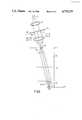
- FIG. 1shows a known apparatus for the repeated imaging of a mask pattern onto a substrate
- FIG. 3shows an alignment arrangement in accordance with the invention
- FIGS. 4, 5, 6 and 7schematically illustrate the principle of and modifications to the alignment method in accordance with the invention.
- FIG. 8illustrates the operation of an order diaphragm in an optical alignment system.
- FIG. 1shows a known apparatus for the repeated imaging of a mask pattern onto a substrate.
- the principle parts of this apparatusare a projection column, in which a pattern C to be imaged is mounted, and a movable substrate table WT by means of which the substrate can be positioned relative to the mask pattern C.
- the projection columnincorporates an illumination system which may comprise a lamp LA, for example a mercury lamp, an elliptical mirror EM, an element IN, also referred to as integrator, which ensures an homogeneous radiation distribution within the projection beam PB and a condensor lens CO.
- the beam PBilluminates the mask pattern C in the mask M, which mask is arranged on a mask table MT.
- the substrate Wis arranged on a substrate table WT, which is supported by for example an air-cushion.
- the projection-lens system PL and the substrate table WTare accommodated in a housing HO which at the bottom is closed by a base plate BP, made of for example granite, and at the top by the mask table MT.
- the mask MAcomprises two alignment marks M 1 and M 2 .
- these markscomprise diffraction gratings, but they may alternatively comprise other marks such as squares or strips which optically differ from their environment.
- the alignment marksare two-dimensional, that is they comprise sub-marks which extend in two mutually perpendicular directions, the X-direction and the Y-direction in FIG. 1.
- the substrate Wfor example a semiconductor substrate, onto which a plurality of images of the pattern C must be formed adjacent each other, comprises a plurality of align marks, preferably also two-dimensional diffraction gratings, of which two gratings P 1 and P 2 are shown in FIG. 1.
- the marks P 1 and P 2are situated outside the areas on the substrate W where the images of the pattern C must be formed.
- the grating marks P 1 and P 2are phase gratings and the grating marks M 1 and M 2 are amplitude gratings.
- FIG. 2shows an example of one of the two identical substrate phase gratings to an enlarged scale.
- a gratingmay comprise four sub-gratings P 1 ,a, P 1 ,b, P 1 ,c and P 1 ,d, of which two sub-gratings P 1 ,b and P 1 ,d serve for alignment in the X-direction and the two other subgratings P 1 ,a and P 1 ,c for alignment in the Y-direction.
- the two sub-gratings P 1 ,b and P 1 ,chave a grating period of, for example, 16 ⁇ m and the sub-gratings P 1 ,a and P 1 ,d have a grating period of, for example, 17.6 ⁇ m.
- the dimensions of each of the sub-gratingsmay be, for example, 200 ⁇ 200 ⁇ m.
- FIG. 3shows an arrangement in accordance with the invention by means of which this alignment can be effected without the frame of the exposure apparatus or a part of this frame being used as a reference, so that for example thermal instabilities of the frame cannot adversely affect the alignment accuracy.
- this apparatusenables the magnification with which the pattern C is imaged on the substrate W to be controlled.
- the alignment arrangementcomprises two separate and identical alignment systems AS 1 and AS 2 which are arranged symmetrically relative to the optical axis AA' of the projection-lens system PL.
- the alignment system AS 1is associated with the mask mark M 2 and the alignment system AS 2 with the mask mark M 1 .
- Corresponding elements of the two alignment systemsbear identical reference numerals, the reference numerals of the elements of the system AS 2 being primed to distinguish them from those of the system AS 1 .
- the alignment system AS 1comprises a radiation source 1, for example a helium-neon laser, which emits an alignment beam b.
- a beam splitter 2reflects this beam to the substrate W.
- the beam splittermay comprise a semi-transparent mirror or a semi-transparent prism, but suitably comprises a polarisation-sensitive prism followed by a ⁇ /4 plate 3, where ⁇ is the wavelength of the beam b.
- the projection-lens system PLfocuses the beam b to form a small radiation spot V of a diameter of the order of 1 mm onto the substrate W. This substrate reflects a part of the beam as the beam b 1 towards the mask M.
- the beam b 1traverses the projection-lens system PL, which system images the radiation spot V on the mask.
- a pre-alignment stationcoupled to the arrangement, for example a station as described in European Patent Application No. 0,164,165, that the radiation spot V is situated on the substrate mark P 1 .
- This markis then imaged onto the mask mark M 2 by the beam b 1 . Allowing for the magnification M of the projection-lens system, the dimension of the mask mark M 2 is adapted to that of the substrate mark P 1 , so that in the case of a correct positioning of the two marks relative to each other the image of the mark P 1 coincides accurately with the mark M 2 .
- the beam b, and the beam b 1 respectivelyOn its way towards and back from the substrate W the beam b, and the beam b 1 respectively, has twice traversed the ⁇ /4 plate 3, the optic axis of this plate extending at an angle of 45° to the direction of polarisation of the linearly polarised beam b issuing from the source 1.
- the beam b 1 traversing the ⁇ /4 platethen has a direction of polarisation which is rotated through 90° relative to the beam b, so that the beam b 1 is transmitted by the polarisation separating prism 2.
- the use of the polarisation separating prism in conjunction with the ⁇ /4 platehas the advantage that the alignment beam can be coupled into the radiation path of the alignment system with a minimal loss of radiation.
- the beam b 1 transmitted by the alignment mark M 2is reflected by a prism 11 and is directed towards a radiation-sensitive detector 13, for example by another reflecting prism 12.
- This detectoris, for example, a composite photodiode comprising, for example, four separate radiation-sensitive areas corresponding to the number of sub-gratings shown in FIG. 2.
- the output signals of these detectorsare a measure of the registration of the mark M 2 with the image of the substrate mark P 1 .
- These signalscan be processed electronically and may be employed to move the mask and the substrate relative to each other by means of drive systems, not shown, in such a way that the image of the mark P 1 coincides with the mark M 2 .
- an automatic alignment arrangementis obtained.
- the split-off beam b 2is incident on a television camera 17, for example by two lenses 15 and 16, which camera is coupled to a monitor, not shown, on which the alignment marks P 1 and M 2 are displayed for the operator of the exposure apparatus. The operator can then establish whether the two marks coincide or can move the substrate W by means of manipulators in order to make the marks coincide.
- FIG. 4schematically indicates how the alignment method in accordance with the invention proceeds.
- the various alignment stepsare designated 1, 2 and 3.
- the alignment systems AS 1 and AS 2are represented by their alignment beams b and b'.
- the substrate WBefore the substrate W is introduced into the exposure apparatus it has been pre-aligned coarsely, that is within an accuracy of some tens of ⁇ m, in a pre-alignment station in such a way that one of the alignment beams b or b' is incident on one of the substrate marks P 1 or P 2 . It is possible to ensure that first the substrate mark P 1 is situated in the radiation path of the system AS 1 , that is in the beam b, which is position 1 in FIG. 4. By means of the system AS 1 and by moving the substrate and the mask relative to each other in the X-direction and the Y-direction the marks P 1 and M 2 are aligned relative to one another.
- the displacement of the substrate and the mask relative to each otheris measured with a very accurate two-dimensional displacement system, for example the interferometer system described in U.S. Pat. No. 4,251,160.
- This systemwhich is represented schematically in FIG. 1 where it bears the reference IF, cooperates very closely with the alignment systems AS 1 and AS 2 .
- the interferometer systemdetermines where the substrate mark P 1 is situated in the coordinate system defined by the interferometer system.
- the position of the image of the mask mark M 2 on the substrateis then known and hence the position in the X-direction and the Y-direction of the local image of the mask pattern C on the substrate.
- the substrate mark P 1is brought into the path of the beam b' and the alignment system AS 2 is employed to align this mark relative to the mask mark M 1 , position 2 in FIG. 4.
- the displacement measuring systemit is then established at which angle and over which distance the substrate is displaced in the coordinate system defined by this measuring system, in order to bring the mark P 1 in register with the mark M 1 .
- Thisnot only gives the angular orientation of the image of the line interconnecting the centres of the mask marks M 1 and M 2 , that is the angular orientation of the mask MA, but the magnification with which the distance between the marks M 1 and M 2 in the mask is imaged in the substrate plane is then also known.
- magnification the mask pattern Cis imaged onto the substrate.
- This informationmay be employed in order to correct the magnification with which the projection-lens system PL forms an image, for example by adapting the distance between the mask and the lens system. This adaptation will hardly affect the imaging quality.
- the substrate mark P 2is moved into the path of the alignment beam b', position 3 in FIG. 4, and, again by means of the system AS 2 , the marks P 2 and M 1 are aligned relative to one another.
- the angular orientation of the substratethat is the angle between the line interconnecting the centres of the marks P 1 and P 2 and the X-direction, is determined.
- the substrateis moved, for example by a combination of a translation and a rotation, so that a possible angular error is eliminated during this alignment.
- the displacement of the substrateis also measured by means of the interferometer system the distance between the substrate marks P 1 and P 2 is also known.
- the repeated imaging of the mask pattern C onto the substrateit is then possible to correct for variations in this distance, which variations may be caused for example, by thermal expansion of the substrate of warping of this substrate.
- the mask and the substrateare not only aligned correctly relative to each other in the X- and Y-direction but an incorrect angular orientation of the line interconnecting the centres of the mask marks relative to the line interconnecting the centres of the substrate marks is also eliminated.
- thisprovides information on the magnification with which the mask pattern is imaged and on the thermal expansions and deformations of the substrate and the mask, enabling the magnification of the exposure apparatus to be adapted and the system for moving the substrate and the mask relative to each other to be calibrated.
- the present alignment methodmerely employs the marks on the substrate and on the mask as reference in conjunction with the displacement-measuring system. It is not needed to refer to the frame or a part of the frame of the apparatus, so that instabilities of this apparatus hardly affect the alignment accuracy.
- a two-dimensional interferometer systemit is also possible to employ another displacement-measuring system, for example a grating measuring system in order to determine the displacement of the substrate. It is merely essential that such a measuring system defines a two-dimensional system of coordinates in the substrate plane and thus a number of reference points in this plane.
- the alignment sequence indicated in FIG. 4is not essential; it is also possible to use a different sequence or different alignment combination. It is important only that two mask marks are aligned relative to three substrate marks, whilst two of the three substrate marks may be the same marks, as is indicated in FIG. 4.
- FIG. 5it is alternatively possible to employ three separate substrate marks, as is indicated schematically in FIG. 5.
- One of these marks P 1is situated at one side of the area W' in which a multiple image of the mask pattern is to be formed and the two other marks P 2 and P 3 are situated at the other side of this area.
- the two substrate marks P 2 and P 3are aligned simultaneously relative to the mask marks M 2 and M 1 , so that in one alignment step four of the above six parameters can be determined.
- the other two parametersare obtained by moving the substrate in such a way that the mark P 1 is situated in register with one of the mask marks M 2 , M 1 and by aligning the mark P 1 relative to one of the marks M 2 , M 1 . Again use is made of the substrate displacement measuring system.
- the projection-lens systemFor imaging the alignment marks onto each other the projection-lens system is employed.
- the image field of this lens systemdoes not impose any restrictions on the alignment arrangement because always only one mask mark is to be imaged onto one substrate mark.
- the substrate marksneed not be situated simultaneously in the image field of the projection-lens system.
- the arrangementmay then be used for different types of projection-lens systems having object fields of different sizes and for various masks with different distances between the mask marks.
- the mark pair P 1 , P 2can be aligned using the method described with reference to FIG. 4. Furthermore, the additional marks P 3 and P 4 can be aligned similarly, in which case again one of the mask marks M 1 , M 2 is aligned relative to the two substrate marks and the second mask mark is aligned relative to one of the substrate marks, which is again effected in conjunction with the substrate-displacement measuring system.
- the alignment method illustrated in FIG. 6is advantageous if the substrate exhibits deformations and instabilities which are not circularly symmetrical but which are oriented at an arbitrary angle to the X-axis.
- the alignment method illustrated in FIG. 6provides information on these deformations and other irregularities, which information is again employed for controlling the displacements and/or magnifications during the repeated exposure of the substrate via the mask pattern.
- substrate marks situated on the substrate outside the area W' in which the mask pattern is to be imaged repeatedlyhave been described, said substrate marks being employed to align the mask pattern and the substrate before repeated imaging is started.
- substrate marksfor example gratings
- These substrate gratings P deach comprise two sub-gratings P d ,1 and P d ,2 whose grating lines extend in the Y-direction and the X-direction respectively and which serve for alignment in the X-direction and the Y-direction respectively.
- These gratingsneed not comprise two sub-gratings with a different grating period for each direction, because the alignment system need only have a very small lock-in range when these gratings are used.
- the purpose of two sub-gratings for each of the two directions, which sub-gratings have different grating periods, in the grating mark shown in FIG. 2is to extend the lock-in range of the alignment system.
- the substrate gratings P d between the areas W d 'enable each mask-pattern image to be aligned separately.
- the method and arrangement described in the foregoingmay then be employed, using the same mask marks as employed for the alignment of the substrate marks situated outside the area W'. It is now also possible to correct for local deformations and other irregularities in the substrate.
- the accuracy of the arrangementis improved substantially by modulating the output signals of the detectors 13 and 13' with a fixed frequency.
- the mask M and thus, for example, the mask mark M 2may be moved periodically.
- FIG. 3A better alternative for obtaining a dynamic alignment signal, which is described in U.S. Pat. No. 4,251,160 and which also enables the accuracy of the alignment arrangement in accordance with the invention to be improved, is illustrated in FIG. 3.
- the beam b 1Before it reaches the mark M 2 the beam b 1 has traversed the polarisation-sensitive separating prism 2, so that this beam is linearly polarised and has a specific direction of polarisation. Subsequently, the beam b 1 traverses a plate 8 of a bi-refringent material, for example quartz whose optic axis makes an angle of 45° to the direction of polarization of the beam which emerges from the prism 2.
- the element 8may comprise a Savart plate or a Wollaston prism. Two beams which are polarised in two mutually perpendicular directions emerge from the plate 8 and at the location of the mask mark M 2 they are offset from one another by a specific distance which is dictated by the geometry of the mark M 2 .
- the detector 13is preceded by a polarisation modulator 18 and a polarisation analyser 19.
- the modulator 18, for example an elasto-optical modulator,is driven by a voltage V B supplied by a generator 20. As a result of this, the direction of polarisation of the beam emerging from the modulator is alternately shifted through 90°.
- the analyser 19has the same principal direction or direction of transmission as the polarisation-sensitive prism 2, so that alternately a first beam and a second beam are transmitted to the detector 13, which first beam has a first direction of polarisation and has formed, for example, a non-shifted image of P 1 on M 2 , and which second beam has a second direction of polarisation and has formed, for example, an image of P 1 on M 2 , which image is shifted by half a grating period.
- the signal from the detector 13is amplified and processed in a phasesensitive detection circuit 21, which also receives the signal V B .
- the output signal S Athen constitutes the desired dynamic alignment signal.
- the alignment marksare gratings substantial advantages can be obtained by arranging a diaphragm in the path of the alignment beam.
- two lenses 10 and 22may be arranged in the radiation path between the grating mark M 2 and the detection system 13.
- the lens 10forms an image of the pupil of the projection-lens system PL and a diaphragm 23 is arranged in the plane of this image.
- FIG. 8schematically shows the principal elements for imaging the gratings P 1 and M 2 onto the detector 13.
- This Figureagain shows a projection-lens system PL.
- This systemcomprises a large number of lens elements which are not shown separately.
- the system PLhas an exit pupil which, viewed from the mask M, is situated in the plane 25. Consequently, the plane 25 is the plane in which the exit pupil is imaged by the lens elements of the system PL which are situated above this plane.
- the beam reflected by the substrate grating P 1is split by this grating into a zero-order beam b 1 (0), two first-order subbeams b 1 (+1) and b 1 (-1), and a plurality of higher-order subbeams which are not shown because they are irrelevant for a correct understanding of the imaging process. All these subbeams together form a faithful image P 1 ' of the grating P 1 in the plane of the mask M. This image is formed by the projection lens system PL. Care is taken that in the case of a correct alignment of the substrate and the mask-pattern image the image P 1 ' coincides with the grating M 2 . As is shown in FIG.
- the subbeams b 1 (0), b 1 (+1) and b 1 (-1), which are diffracted in different diffraction orders,are spatially separated from each other in the plane 25.
- a diaphragm with apertures at the location of the subbeams b 1 (+1) and b 1 (- 1)may be arranged in this plane, so that the zero-order subbeam and the second-order and higher-order subbeams are suppressed.
- the zero-order subbeamdoes not contain any information on the position of the grating P 1 .
- the intensity of this subbeammay be substantial in comparison with the intensity of the first-order subbeam.
- the contrast in the image P 1 'can be increased substantially. Since the second-order and higher-order subbeams are suppressed, irregularities in the grating P 1 do not affect the alignment signal. If only the first-order subbeams are used the second harmonic of the grating P 1 is.
- the image P 1 'has a period which is half that of the grating P 1 . If care is taken that the grating period of the grating M 2 is equal to that of the image P 1 ', that is equal to 1/2M times the grating period of the grating P 1 , the accuracy with which the gratings M 2 and P 1 are aligned is twice as large as in the case that the entire beam b 1 is used for imaging.
- a diaphragm which performs the function described aboveis arranged outside the projection-lens system PL.
- This diaphragmcan perform its function only if it is arranged in a plane where the subbeams of different diffraction orders are adequately separated.
- Such a planeis obtained by means of the lens 10 which images the plane 25, which is the plane of the pupil of the system PL, in a plane 25'.
- the diaphragm 23is arranged in the last-mentioned plane.
- the second lens 22, together with the lens 10,ensures that the grating M 2 and the image P 1 ' of the grating P 1 which is superimposed thereon is imaged onto the detector 13.
- the diaphragmhas apertures 26 and 27.
- the beam b 1As the beam b 1 is not filtered before it is incident on the grating M 2 it comprises, in principle, all diffraction orders.
- the grating period of the grating M 2dictates at which angles the subbeams of the various diffraction orders are diffracted by this grating, that is which subbeams issuing from the substrate grating P 1 and the mask grating M 2 are transmitted to the detector 13. Care has been taken that the components of the first-order subbeams from the grating P 1 which are not diffracted by the grating M 2 , that is the zero-order components of the beams b 1 (+1) and b 1 (-1), are transmitted. These beam components may be represented by: b 1 (+1,0) and b 1 (-1,0) in which the second index is the diffraction order of the mask grating M 2 .
- the subbeam b 1 (+1) which is diffracted in the +1 order by the grating M 2that is the subbeams b 1 (+1,+1) coincides with the subbeam b 1 (-1,0)
- the subbeam b 1 (+1,+1)is also transmitted by the aperture 27.
- the component of the subbeam b 1 (-1) diffracted in the -1 order by the grating M 2that is the subbeam b 1 (-1,-1), coincides with the subbeam b 1 (+1,0), so that the subbeam b 1 (-1,-1) is transmitted to the detector 13 by the aperture 26.
- the part of the zero-order subbeam b 1 (0) which issues from the grating P 1 and which is diffracted in the +1 order or -1 order by the grating M 2falls outside the apertures 26 and 27, if it can enter the lens 22 at all. It is ensured that the parts of the first-order subbeams which issue from the grating P 1 and which are diffracted in the zero-order and the first-orders by the grating M 2 are transmitted to the detector, with all the consequent advantages.
- FIG. 8only illustrates the situation in one plane.
- the gratings P 1 and M 2are two-dimensional gratings diffraction also occurs in a second plane perpendicular to the plane of drawing in FIG. 8. Therefore, in addition to the apertures 26 and 27 the diaphragm 23 has two further apertures 28 and 29 which in the same way as the apertures 26 and 27 for the first dimension transmit similar diffraction orders for the second dimension.
- the projection-lens system PLis designed for the wavelength of the projection beam PB, which should be as low as possible in view of the desired high resolution, and alignment is effected with a beam b of a different wavelength
- the magnification with which the system PL images the grating P 1may differ slightly from the desired magnification and, moreover, the image of P 1 may be situated slightly outside the plane of the mask M.
- a system 4comprising at least two elements is arranged in the path of the beam b 1 .
- the system 4is shown to an enlarged scale in the bottom-left part of FIG. 3 and comprises three additional mirrors 5, 6 and 7, which prolong the radiation path for the alignment beam b 1 , and a plano-convex lens 9.
- the mirrors 5, 6 and 7 together with the mirror 2may be arranged on a block of a transparent material, for example, glass, on whose bottom surface the ⁇ /4 plate on whose top surface the lens 9 and the birefringent plate 8, Savart plate or Wollaston prism are arranged.
- the combination of the mirrors 5, 6 and 7 and the lens 9 in conjunction with the projection-lens system PLensures that he image of the mark P 1 has the correct size and is formed at the correct axial position.
- An alternative to the assembly of mirrors 5, 6 and 7 and the lens 9may be a combination of a plano-convex lens 4 1 and a biconvex lens 4 2 , as is shown in broken lines in the bottom-left part of FIG. 3.
- the inventionmay be employed in all cases where a pattern of very fine detail should be transferred to a substrate and this pattern should be aligned very accurately relative to the substrate.
- Examples of theseare apparatuses employed in the fabrication of integrated optical systems of magnetic domain memories.
- the apparatus with which a pattern is imagedneed not be an imaging apparatus of the repeater type; the invention may also be useful in an apparatus in which a pattern is imaged only once on a substrate.
Landscapes
- Physics & Mathematics (AREA)
- General Physics & Mathematics (AREA)
- Exposure And Positioning Against Photoresist Photosensitive Materials (AREA)
- Exposure Of Semiconductors, Excluding Electron Or Ion Beam Exposure (AREA)
- Length Measuring Devices By Optical Means (AREA)
Abstract
Description
Claims (20)
Applications Claiming Priority (2)
| Application Number | Priority Date | Filing Date | Title |
|---|---|---|---|
| NL8600639ANL8600639A (en) | 1986-03-12 | 1986-03-12 | METHOD FOR ALIGNING A MASK AND A SUBSTRATE AND DEVICE FOR CARRYING OUT THE METHOD |
| NL8600639 | 1986-03-12 |
Publications (1)
| Publication Number | Publication Date |
|---|---|
| US4778275Atrue US4778275A (en) | 1988-10-18 |
Family
ID=19847702
Family Applications (1)
| Application Number | Title | Priority Date | Filing Date |
|---|---|---|---|
| US06/910,710Expired - LifetimeUS4778275A (en) | 1986-03-12 | 1986-09-24 | Method of aligning a mask and a substrate relative to each other and arrangement for carrying out the method |
Country Status (5)
| Country | Link |
|---|---|
| US (1) | US4778275A (en) |
| EP (1) | EP0237109B1 (en) |
| JP (1) | JP2677558B2 (en) |
| DE (1) | DE3776805D1 (en) |
| NL (1) | NL8600639A (en) |
Cited By (64)
| Publication number | Priority date | Publication date | Assignee | Title |
|---|---|---|---|---|
| US5100237A (en)* | 1989-04-20 | 1992-03-31 | Asm Lithography | Apparatus for projecting a mask pattern on a substrate |
| US5137363A (en)* | 1986-06-04 | 1992-08-11 | Canon Kabushiki Kaisha | Projection exposure apparatus |
| US5481362A (en)* | 1990-07-16 | 1996-01-02 | Asm Lithography | Apparatus for projecting a mask pattern on a substrate |
| US5483345A (en)* | 1994-09-06 | 1996-01-09 | Mrs Technology, Inc. | Alignment system for use in lithography utilizing a spherical reflector having a centered etched-on projection object |
| WO1997032241A1 (en)* | 1996-02-15 | 1997-09-04 | Philips Electronics N.V. | Method of determining the radiation dose in a lithographic apparatus, and test mask and apparatus for performing the method |
| WO1997035234A1 (en)* | 1996-03-15 | 1997-09-25 | Philips Electronics N.V. | Alignment device and lithographic apparatus provided with such a device |
| US5673101A (en)* | 1994-06-02 | 1997-09-30 | U.S. Philips Corporation | Method of repetitively imaging a mask pattern on a substrate, and apparatus for performing the method |
| US5674650A (en)* | 1994-08-02 | 1997-10-07 | U.S. Philips Corporation | Method of repetitively imaging a mask pattern on a substrate, and apparatus for performing the method |
| US5721607A (en)* | 1994-12-15 | 1998-02-24 | Nikon Corporation | Alignment method and apparatus |
| US5801832A (en)* | 1991-02-07 | 1998-09-01 | Asm Lithography | Method of and device for repetitively imaging a mask pattern on a substrate using five measuring axes |
| WO1999034258A1 (en)* | 1997-12-29 | 1999-07-08 | Asm Lithography B.V. | Alignment device and lithographic apparatus comprising such a device |
| US6084673A (en)* | 1996-03-04 | 2000-07-04 | Asm Lithography B.V. | Lithographic apparatus for step-and-scan imaging of mask pattern with interferometer mirrors on the mask and wafer holders |
| US6122058A (en)* | 1997-12-22 | 2000-09-19 | Asm Lithography B.V. | Interferometer system with two wavelengths, and lithographic apparatus provided with such a system |
| US6197481B1 (en) | 1998-09-17 | 2001-03-06 | Taiwan Semiconductor Manufacturing Company | Wafer alignment marks protected by photoresist |
| US6243203B1 (en) | 1998-04-24 | 2001-06-05 | U.S. Philips Corporation | Optical system with anti-reflection coating |
| US20010014170A1 (en)* | 2000-02-10 | 2001-08-16 | Willems Van Dijk Marcus J.H. | Object positioning method for a lithographic projection apparatus |
| US6294296B1 (en) | 1999-10-11 | 2001-09-25 | Carl-Zeiss-Stiftung | Method and device for mutually aligning a mask pattern formed in a mask and a substrate |
| US6297876B1 (en) | 1997-03-07 | 2001-10-02 | Asm Lithography B.V. | Lithographic projection apparatus with an alignment system for aligning substrate on mask |
| US6368763B2 (en) | 1998-11-23 | 2002-04-09 | U.S. Philips Corporation | Method of detecting aberrations of an optical imaging system |
| US20020080365A1 (en)* | 2000-12-27 | 2002-06-27 | Koninklijke Philips Electronics N. V. | Method of measuring alignment of a substrate with respect to a reference alignment mark |
| US20020080364A1 (en)* | 2000-12-27 | 2002-06-27 | Koninklijke Philips Electronics N.V. | Method of measuring overlay |
| US6417922B1 (en) | 1997-12-29 | 2002-07-09 | Asml Netherlands B.V. | Alignment device and lithographic apparatus comprising such a device |
| US6462818B1 (en) | 2000-06-22 | 2002-10-08 | Kla-Tencor Corporation | Overlay alignment mark design |
| US6486954B1 (en) | 2000-09-01 | 2002-11-26 | Kla-Tencor Technologies Corporation | Overlay alignment measurement mark |
| US6507388B2 (en)* | 1999-12-23 | 2003-01-14 | Asml Netherlands B.V. | Interferometric alignment system for use in vacuum-based lithographic apparatus |
| US20030043356A1 (en)* | 1990-11-15 | 2003-03-06 | Nikon Corporation | Projection exposure apparatus and method |
| US6544694B2 (en) | 2000-03-03 | 2003-04-08 | Koninklijke Philips Electronics N.V. | Method of manufacturing a device by means of a mask phase-shifting mask for use in said method |
| US6636293B1 (en) | 1990-08-21 | 2003-10-21 | Nikon Corporation | Exposure method and apparatus having a decreased light intensity distribution |
| US20030223630A1 (en)* | 2002-02-15 | 2003-12-04 | Kla-Tencor Corporation | Overlay metrology and control method |
| US6665050B2 (en) | 1990-11-15 | 2003-12-16 | Nikon Corporation | Projection exposure methods using difracted light with increased intensity portions spaced from the optical axis |
| US6677601B2 (en)* | 1995-02-01 | 2004-01-13 | Nikon Corporation | Method of detecting position of mark on substrate, position detection apparatus using this method, and exposure apparatus using this position detection apparatus |
| US6710854B2 (en) | 1991-09-11 | 2004-03-23 | Nikon Corporation | Projection exposure apparatus |
| US20040066517A1 (en)* | 2002-09-05 | 2004-04-08 | Hsu-Ting Huang | Interferometry-based method and apparatus for overlay metrology |
| US20040114143A1 (en)* | 2002-09-20 | 2004-06-17 | Asml Netherlands B.V. | Marker structure for optical alignment of a substrate, a substrate including such a marker structure, an alignment method for aligning to such a marker structure, and a lithographic projection apparatus |
| US20040166444A1 (en)* | 2003-02-25 | 2004-08-26 | Canon Kabushiki Kaisha | Method of producing substrate with mark, program for reading mark, and apparatus for reading mark |
| US20040211921A1 (en)* | 1999-12-22 | 2004-10-28 | Asml Netherlands B.V. | Position measuring device, position measuring system, lithographic apparatus, and device manufacturing method |
| US20040212796A1 (en)* | 2003-04-25 | 2004-10-28 | Michael Adel | Method and mark for metrology of phase errors on phase shift masks |
| US20040227919A1 (en)* | 1990-11-15 | 2004-11-18 | Nikon Corporation | Projection exposure apparatus and method |
| US20040233411A1 (en)* | 1990-11-15 | 2004-11-25 | Nikon Corporation | Projection exposure apparatus and method |
| US20050007572A1 (en)* | 2003-05-30 | 2005-01-13 | George Richard Alexander | Lithographic apparatus and device manufacturing method |
| US20050089762A1 (en)* | 2003-10-24 | 2005-04-28 | Joseph Consolini | Methods and apparatuses for applying wafer-alignment marks |
| US6921916B2 (en) | 2000-08-30 | 2005-07-26 | Kla -Tenocor Technologies Corporation | Overlay marks, methods of overlay mark design and methods of overlay measurements |
| US20050254030A1 (en)* | 2004-05-14 | 2005-11-17 | Asml Netherlands B.V. | Alignment system and method and device manufactured thereby |
| US6967710B2 (en) | 1990-11-15 | 2005-11-22 | Nikon Corporation | Projection exposure apparatus and method |
| US7046361B1 (en)* | 2002-04-04 | 2006-05-16 | Nanometrics Incorporated | Positioning two elements using an alignment target with a designed offset |
| US20060138410A1 (en)* | 2004-12-29 | 2006-06-29 | Asml Netherlands B.V. | Method for measuring information about a substrate, and a substrate for use in a lithographic apparatus |
| US20060160029A1 (en)* | 2001-05-18 | 2006-07-20 | Peter Dirksen | Lithographic method of manufacturing a device |
| US20070259290A1 (en)* | 2006-04-27 | 2007-11-08 | Nikon Corporation | Measuring and/or inspecting method, measuring and/or inspecting apparatus, exposure method, device manufacturing method, and device manufacturing apparatus |
| US7346878B1 (en) | 2003-07-02 | 2008-03-18 | Kla-Tencor Technologies Corporation | Apparatus and methods for providing in-chip microtargets for metrology or inspection |
| US20090018693A1 (en)* | 2007-07-13 | 2009-01-15 | Z-Laser Optoelektronik Gmbh | Apparatus for Projecting an Optical Marking on the Surface of an Article |
| US20090026657A1 (en)* | 2007-07-20 | 2009-01-29 | Molecular Imprints, Inc. | Alignment System and Method for a Substrate in a Nano-Imprint Process |
| US7557921B1 (en) | 2005-01-14 | 2009-07-07 | Kla-Tencor Technologies Corporation | Apparatus and methods for optically monitoring the fidelity of patterns produced by photolitographic tools |
| US7608468B1 (en) | 2003-07-02 | 2009-10-27 | Kla-Tencor Technologies, Corp. | Apparatus and methods for determining overlay and uses of same |
| US20090323039A1 (en)* | 2008-06-27 | 2009-12-31 | Asml Netherlands B.V. | Correction Method for Non-Uniform Reticle Heating in a Lithographic Apparatus |
| US7656504B1 (en) | 1990-08-21 | 2010-02-02 | Nikon Corporation | Projection exposure apparatus with luminous flux distribution |
| US7759029B2 (en) | 2001-05-23 | 2010-07-20 | Asml Netherlands B.V. | Substrate provided with an alignment mark in a substantially transmissive process layer, mask for exposing said mark, device manufacturing method, and device manufactured thereby |
| CN101487992B (en)* | 2009-03-04 | 2010-10-20 | 上海微电子装备有限公司 | Silicon slice mark capturing system and method |
| US8138498B2 (en) | 2000-08-30 | 2012-03-20 | Kla-Tencor Technologies Corporation | Apparatus and methods for determining overlay of structures having rotational or mirror symmetry |
| US8953173B2 (en) | 2008-04-04 | 2015-02-10 | Carl Zeiss Smt Gmbh | Apparatus for microlithographic projection exposure and apparatus for inspecting a surface of a substrate |
| US9927718B2 (en) | 2010-08-03 | 2018-03-27 | Kla-Tencor Corporation | Multi-layer overlay metrology target and complimentary overlay metrology measurement systems |
| US10451412B2 (en) | 2016-04-22 | 2019-10-22 | Kla-Tencor Corporation | Apparatus and methods for detecting overlay errors using scatterometry |
| US10890436B2 (en) | 2011-07-19 | 2021-01-12 | Kla Corporation | Overlay targets with orthogonal underlayer dummyfill |
| CN117080119A (en)* | 2023-08-17 | 2023-11-17 | 泓浒(苏州)半导体科技有限公司 | Method and system for detecting and calibrating semiconductor wafer position |
| US11982521B2 (en)* | 2017-02-23 | 2024-05-14 | Nikon Corporation | Measurement of a change in a geometrical characteristic and/or position of a workpiece |
Families Citing this family (3)
| Publication number | Priority date | Publication date | Assignee | Title |
|---|---|---|---|---|
| JPH0797545B2 (en)* | 1986-07-04 | 1995-10-18 | 株式会社トプコン | Optical alignment device for projection exposure apparatus |
| JPS63229305A (en)* | 1987-03-18 | 1988-09-26 | Nikon Corp | pattern detection device |
| NL9000503A (en)* | 1990-03-05 | 1991-10-01 | Asm Lithography Bv | APPARATUS AND METHOD FOR IMAGING A MASK PATTERN ON A SUBSTRATE. |
Citations (3)
| Publication number | Priority date | Publication date | Assignee | Title |
|---|---|---|---|---|
| US4062623A (en)* | 1975-04-07 | 1977-12-13 | Canon Kabushiki Kaisha | Device for observing an object |
| US4251160A (en)* | 1976-06-17 | 1981-02-17 | U.S. Philips Corporation | Method and arrangement for aligning a mask pattern relative to a semiconductor substrate |
| US4573791A (en)* | 1979-04-03 | 1986-03-04 | Optimetrix Corporation | Step-and-repeat projection alignment and exposure system |
Family Cites Families (9)
| Publication number | Priority date | Publication date | Assignee | Title |
|---|---|---|---|---|
| JPS54157478A (en)* | 1978-06-01 | 1979-12-12 | Canon Inc | Alignment method |
| EP0017759B1 (en)* | 1979-04-03 | 1985-09-04 | Eaton-Optimetrix Inc. | Improved step-and-repeat projection alignment and exposure system |
| JPS55135831A (en)* | 1979-04-03 | 1980-10-23 | Optimetrix Corp | Improved stepprepetion projectionnmatching exposer |
| JPS57183033A (en)* | 1981-05-06 | 1982-11-11 | Toshiba Corp | Method for wafer exposure and device thereof |
| JPS59161025A (en)* | 1983-03-04 | 1984-09-11 | Hitachi Ltd | Reduction projection exposure equipment |
| JPS6021051A (en)* | 1983-07-14 | 1985-02-02 | Nippon Telegr & Teleph Corp <Ntt> | Lens projection and exposure method and its device |
| JPS60179745A (en)* | 1984-02-28 | 1985-09-13 | Nippon Kogaku Kk <Nikon> | Pattern transfer method and transfer device |
| JPS61256634A (en)* | 1985-05-10 | 1986-11-14 | Hitachi Ltd | &?reduction projection type alignment |
| JPS62154263A (en)* | 1985-12-25 | 1987-07-09 | Toshiba Corp | signal processing circuit |
- 1986
- 1986-03-12NLNL8600639Apatent/NL8600639A/ennot_activeApplication Discontinuation
- 1986-09-24USUS06/910,710patent/US4778275A/ennot_activeExpired - Lifetime
- 1987
- 1987-02-26EPEP87200341Apatent/EP0237109B1/ennot_activeExpired
- 1987-02-26DEDE8787200341Tpatent/DE3776805D1/ennot_activeExpired - Lifetime
- 1987-03-11JPJP62054290Apatent/JP2677558B2/ennot_activeExpired - Fee Related
Patent Citations (3)
| Publication number | Priority date | Publication date | Assignee | Title |
|---|---|---|---|---|
| US4062623A (en)* | 1975-04-07 | 1977-12-13 | Canon Kabushiki Kaisha | Device for observing an object |
| US4251160A (en)* | 1976-06-17 | 1981-02-17 | U.S. Philips Corporation | Method and arrangement for aligning a mask pattern relative to a semiconductor substrate |
| US4573791A (en)* | 1979-04-03 | 1986-03-04 | Optimetrix Corporation | Step-and-repeat projection alignment and exposure system |
Non-Patent Citations (2)
| Title |
|---|
| "Automatic Alignment System for Optical Projection Printing" Bouwhuis et al, IEEE Transactions on Electron Devices, vol. Ed 26, #4, 4/1979. |
| Automatic Alignment System for Optical Projection Printing Bouwhuis et al, IEEE Transactions on Electron Devices, vol. Ed 26, 4, 4/1979.* |
Cited By (145)
| Publication number | Priority date | Publication date | Assignee | Title |
|---|---|---|---|---|
| US5137363A (en)* | 1986-06-04 | 1992-08-11 | Canon Kabushiki Kaisha | Projection exposure apparatus |
| US5100237A (en)* | 1989-04-20 | 1992-03-31 | Asm Lithography | Apparatus for projecting a mask pattern on a substrate |
| US5481362A (en)* | 1990-07-16 | 1996-01-02 | Asm Lithography | Apparatus for projecting a mask pattern on a substrate |
| US6636293B1 (en) | 1990-08-21 | 2003-10-21 | Nikon Corporation | Exposure method and apparatus having a decreased light intensity distribution |
| US7656504B1 (en) | 1990-08-21 | 2010-02-02 | Nikon Corporation | Projection exposure apparatus with luminous flux distribution |
| US6704092B2 (en) | 1990-11-15 | 2004-03-09 | Nikon Corporation | Projection exposure method and apparatus that produces an intensity distribution on a plane substantially conjugate to a projection optical system pupil plane |
| US20040233411A1 (en)* | 1990-11-15 | 2004-11-25 | Nikon Corporation | Projection exposure apparatus and method |
| US6710855B2 (en) | 1990-11-15 | 2004-03-23 | Nikon Corporation | Projection exposure apparatus and method |
| US6885433B2 (en) | 1990-11-15 | 2005-04-26 | Nikon Corporation | Projection exposure apparatus and method |
| US20030043356A1 (en)* | 1990-11-15 | 2003-03-06 | Nikon Corporation | Projection exposure apparatus and method |
| US6967710B2 (en) | 1990-11-15 | 2005-11-22 | Nikon Corporation | Projection exposure apparatus and method |
| US6665050B2 (en) | 1990-11-15 | 2003-12-16 | Nikon Corporation | Projection exposure methods using difracted light with increased intensity portions spaced from the optical axis |
| US6897942B2 (en) | 1990-11-15 | 2005-05-24 | Nikon Corporation | Projection exposure apparatus and method |
| US20040227919A1 (en)* | 1990-11-15 | 2004-11-18 | Nikon Corporation | Projection exposure apparatus and method |
| US5801832A (en)* | 1991-02-07 | 1998-09-01 | Asm Lithography | Method of and device for repetitively imaging a mask pattern on a substrate using five measuring axes |
| US6864959B2 (en) | 1991-09-11 | 2005-03-08 | Nikon Corporation | Projection exposure apparatus |
| US6710854B2 (en) | 1991-09-11 | 2004-03-23 | Nikon Corporation | Projection exposure apparatus |
| US5673101A (en)* | 1994-06-02 | 1997-09-30 | U.S. Philips Corporation | Method of repetitively imaging a mask pattern on a substrate, and apparatus for performing the method |
| US5674650A (en)* | 1994-08-02 | 1997-10-07 | U.S. Philips Corporation | Method of repetitively imaging a mask pattern on a substrate, and apparatus for performing the method |
| WO1996007870A1 (en)* | 1994-09-06 | 1996-03-14 | Mrs Technology, Inc. | Simple light probe for large area lithography alignment system |
| US5483345A (en)* | 1994-09-06 | 1996-01-09 | Mrs Technology, Inc. | Alignment system for use in lithography utilizing a spherical reflector having a centered etched-on projection object |
| US5721607A (en)* | 1994-12-15 | 1998-02-24 | Nikon Corporation | Alignment method and apparatus |
| US7053390B2 (en) | 1995-02-01 | 2006-05-30 | Nikon Corporation | Method of detecting position of mark on substrate, position detection apparatus using this method, and exposure apparatus using this position detection apparatus |
| US20050051742A1 (en)* | 1995-02-01 | 2005-03-10 | Nikon Corporation | Method of detecting position of mark on substrate, position detection apparatus using this method, and exposure apparatus using this position detection apparatus |
| US6677601B2 (en)* | 1995-02-01 | 2004-01-13 | Nikon Corporation | Method of detecting position of mark on substrate, position detection apparatus using this method, and exposure apparatus using this position detection apparatus |
| US7109508B2 (en) | 1995-02-01 | 2006-09-19 | Nikon Corporation | Method of detecting position of mark on substrate, position detection apparatus using this method, and exposure apparatus using this position detection apparatus |
| WO1997032241A1 (en)* | 1996-02-15 | 1997-09-04 | Philips Electronics N.V. | Method of determining the radiation dose in a lithographic apparatus, and test mask and apparatus for performing the method |
| US6084673A (en)* | 1996-03-04 | 2000-07-04 | Asm Lithography B.V. | Lithographic apparatus for step-and-scan imaging of mask pattern with interferometer mirrors on the mask and wafer holders |
| WO1997035234A1 (en)* | 1996-03-15 | 1997-09-25 | Philips Electronics N.V. | Alignment device and lithographic apparatus provided with such a device |
| US5917604A (en)* | 1996-03-15 | 1999-06-29 | U.S. Philips Corporation | Alignment device and lithographic apparatus provided with such a device |
| US6297876B1 (en) | 1997-03-07 | 2001-10-02 | Asm Lithography B.V. | Lithographic projection apparatus with an alignment system for aligning substrate on mask |
| US6122058A (en)* | 1997-12-22 | 2000-09-19 | Asm Lithography B.V. | Interferometer system with two wavelengths, and lithographic apparatus provided with such a system |
| WO1999034258A1 (en)* | 1997-12-29 | 1999-07-08 | Asm Lithography B.V. | Alignment device and lithographic apparatus comprising such a device |
| US6160622A (en)* | 1997-12-29 | 2000-12-12 | Asm Lithography, B.V. | Alignment device and lithographic apparatus comprising such a device |
| US6417922B1 (en) | 1997-12-29 | 2002-07-09 | Asml Netherlands B.V. | Alignment device and lithographic apparatus comprising such a device |
| US6243203B1 (en) | 1998-04-24 | 2001-06-05 | U.S. Philips Corporation | Optical system with anti-reflection coating |
| US6197481B1 (en) | 1998-09-17 | 2001-03-06 | Taiwan Semiconductor Manufacturing Company | Wafer alignment marks protected by photoresist |
| US6368763B2 (en) | 1998-11-23 | 2002-04-09 | U.S. Philips Corporation | Method of detecting aberrations of an optical imaging system |
| US6294296B1 (en) | 1999-10-11 | 2001-09-25 | Carl-Zeiss-Stiftung | Method and device for mutually aligning a mask pattern formed in a mask and a substrate |
| US6894261B2 (en)* | 1999-12-22 | 2005-05-17 | Asml Netherlands B.V. | Position measuring system for use in lithographic apparatus |
| US20040211921A1 (en)* | 1999-12-22 | 2004-10-28 | Asml Netherlands B.V. | Position measuring device, position measuring system, lithographic apparatus, and device manufacturing method |
| US6875992B2 (en) | 1999-12-22 | 2005-04-05 | Asml Netherlands B.V. | Position measuring device, position measuring system, lithographic apparatus, and device manufacturing method |
| US6876436B2 (en) | 1999-12-23 | 2005-04-05 | Asml Netherlands, B.V. | Interferometric alignment system for use in vacuum-based lithographic apparatus |
| US6507388B2 (en)* | 1999-12-23 | 2003-01-14 | Asml Netherlands B.V. | Interferometric alignment system for use in vacuum-based lithographic apparatus |
| US20030095241A1 (en)* | 1999-12-23 | 2003-05-22 | Asml Netherlands B.V. | Interferometric alignment system for use in vacuum-based lithographic apparatus |
| US7397940B2 (en)* | 2000-02-10 | 2008-07-08 | Asml Netherlands B.V. | Object positioning method for a lithographic projection apparatus |
| US20010014170A1 (en)* | 2000-02-10 | 2001-08-16 | Willems Van Dijk Marcus J.H. | Object positioning method for a lithographic projection apparatus |
| US6544694B2 (en) | 2000-03-03 | 2003-04-08 | Koninklijke Philips Electronics N.V. | Method of manufacturing a device by means of a mask phase-shifting mask for use in said method |
| US6462818B1 (en) | 2000-06-22 | 2002-10-08 | Kla-Tencor Corporation | Overlay alignment mark design |
| US6894783B2 (en) | 2000-06-22 | 2005-05-17 | Kla-Tencor Corporation | Overlay alignment mark design |
| US6580505B1 (en) | 2000-06-22 | 2003-06-17 | Kla-Tencor Corporation | Overlay alignment mark design |
| US20050174574A1 (en)* | 2000-06-22 | 2005-08-11 | Kla-Tencor Corporation | Overlay alignment mark design |
| US7102749B2 (en) | 2000-06-22 | 2006-09-05 | Kla-Tencor | Overlay alignment mark design |
| US20060204073A1 (en)* | 2000-08-30 | 2006-09-14 | Kla-Tencor Corporation | Overlay marks, methods of overlay mark design and methods of overlay measurements |
| US20080023855A1 (en)* | 2000-08-30 | 2008-01-31 | Kla-Tencor Corporation | Overlay marks, methods of overlay mark design and methods of overlay measurements |
| US7177457B2 (en) | 2000-08-30 | 2007-02-13 | Kla-Tencor Corporation | Overlay marks, methods of overlay mark design and methods of overlay measurements |
| US7879627B2 (en) | 2000-08-30 | 2011-02-01 | Kla-Tencor Technologies Corporation | Overlay marks and methods of manufacturing such marks |
| US8138498B2 (en) | 2000-08-30 | 2012-03-20 | Kla-Tencor Technologies Corporation | Apparatus and methods for determining overlay of structures having rotational or mirror symmetry |
| US8330281B2 (en)* | 2000-08-30 | 2012-12-11 | Kla-Tencor Technologies Corporation | Overlay marks, methods of overlay mark design and methods of overlay measurements |
| US6921916B2 (en) | 2000-08-30 | 2005-07-26 | Kla -Tenocor Technologies Corporation | Overlay marks, methods of overlay mark design and methods of overlay measurements |
| USRE45245E1 (en) | 2000-08-30 | 2014-11-18 | Kla-Tencor Corporation | Apparatus and methods for determining overlay of structures having rotational or mirror symmetry |
| US9182680B2 (en) | 2000-08-30 | 2015-11-10 | Kla-Tencor Corporation | Apparatus and methods for determining overlay of structures having rotational or mirror symmetry |
| US20060177120A1 (en)* | 2000-08-30 | 2006-08-10 | Kla-Tencor Corporation | Overlay marks, methods of overlay mark design and methods of overlay measurements |
| US7317824B2 (en) | 2000-08-30 | 2008-01-08 | Kla-Tencor Technologies Corporation | Overlay marks, methods of overlay mark design and methods of overlay measurements |
| US9702693B2 (en) | 2000-08-30 | 2017-07-11 | Kla-Tencor Corporation | Apparatus for measuring overlay errors |
| US7068833B1 (en) | 2000-08-30 | 2006-06-27 | Kla-Tencor Corporation | Overlay marks, methods of overlay mark design and methods of overlay measurements |
| US7181057B2 (en) | 2000-08-30 | 2007-02-20 | Kla-Tencor Technologies Corporation | Overlay marks, methods of overlay mark design and methods of overlay measurements |
| US7274814B2 (en) | 2000-08-30 | 2007-09-25 | Kla-Tencor Corporation | Overlay marks, methods of overlay mark design and methods of overlay measurements |
| US6985618B2 (en) | 2000-08-30 | 2006-01-10 | Kla-Tencor Technologies Corporation | Overlay marks, methods of overlay mark design and methods of overlay measurements |
| US20060039595A1 (en)* | 2000-08-30 | 2006-02-23 | Kla-Tencor Technologies Corporation | Overlay marks, methods of overlay mark design and methods of overlay measurements |
| US7355291B2 (en) | 2000-08-30 | 2008-04-08 | Kla-Tencor Technologies Corporation | Overlay marks, methods of overlay mark design and methods of overlay measurements |
| US20090291513A1 (en)* | 2000-08-30 | 2009-11-26 | Kla-Tencor Corporation | Overlay marks, methods of overlay mark design and methods of overlay measurements |
| US9347879B2 (en) | 2000-08-30 | 2016-05-24 | Kla-Tencor Corporation | Apparatus and methods for detecting overlay errors using scatterometry |
| US6486954B1 (en) | 2000-09-01 | 2002-11-26 | Kla-Tencor Technologies Corporation | Overlay alignment measurement mark |
| US20020080365A1 (en)* | 2000-12-27 | 2002-06-27 | Koninklijke Philips Electronics N. V. | Method of measuring alignment of a substrate with respect to a reference alignment mark |
| US6937344B2 (en) | 2000-12-27 | 2005-08-30 | Asml Netherlands B.V. | Method of measuring overlay |
| US20020080364A1 (en)* | 2000-12-27 | 2002-06-27 | Koninklijke Philips Electronics N.V. | Method of measuring overlay |
| US20050231698A1 (en)* | 2000-12-27 | 2005-10-20 | Asml Netherlands B.V. | Method of measuring alignment of a substrate with respect to a reference alignment mark |
| US20050231732A1 (en)* | 2000-12-27 | 2005-10-20 | Asml Netherlands B.V. | Method of measuring overlay |
| US7277185B2 (en) | 2000-12-27 | 2007-10-02 | Asml Netherlands B.V. | Method of measuring overlay |
| US6937334B2 (en) | 2000-12-27 | 2005-08-30 | Asml Netherlands B.V. | Method of measuring alignment of a substrate with respect to a reference alignment mark |
| US7095499B2 (en) | 2000-12-27 | 2006-08-22 | Asml Netherlands B.V. | Method of measuring alignment of a substrate with respect to a reference alignment mark |
| US20060160029A1 (en)* | 2001-05-18 | 2006-07-20 | Peter Dirksen | Lithographic method of manufacturing a device |
| US7659041B2 (en) | 2001-05-18 | 2010-02-09 | Koninklijke Philips Electronics N.V. | Lithographic method of manufacturing a device |
| US7759029B2 (en) | 2001-05-23 | 2010-07-20 | Asml Netherlands B.V. | Substrate provided with an alignment mark in a substantially transmissive process layer, mask for exposing said mark, device manufacturing method, and device manufactured thereby |
| US7804994B2 (en) | 2002-02-15 | 2010-09-28 | Kla-Tencor Technologies Corporation | Overlay metrology and control method |
| US20030223630A1 (en)* | 2002-02-15 | 2003-12-04 | Kla-Tencor Corporation | Overlay metrology and control method |
| US7046361B1 (en)* | 2002-04-04 | 2006-05-16 | Nanometrics Incorporated | Positioning two elements using an alignment target with a designed offset |
| US20040066517A1 (en)* | 2002-09-05 | 2004-04-08 | Hsu-Ting Huang | Interferometry-based method and apparatus for overlay metrology |
| US20060081790A1 (en)* | 2002-09-20 | 2006-04-20 | Asml Netherlands B.V. | Alignment systems and methods for lithographic systems |
| US20060086910A1 (en)* | 2002-09-20 | 2006-04-27 | Asml Netherlands B.V. | Alignment systems and methods for lithographic systems |
| US20070176128A1 (en)* | 2002-09-20 | 2007-08-02 | Asml Netherlands B.V. | Alignment systems and methods for lithographic systems |
| US7112813B2 (en) | 2002-09-20 | 2006-09-26 | Asml Netherlands B.V. | Device inspection method and apparatus using an asymmetric marker |
| US20040114143A1 (en)* | 2002-09-20 | 2004-06-17 | Asml Netherlands B.V. | Marker structure for optical alignment of a substrate, a substrate including such a marker structure, an alignment method for aligning to such a marker structure, and a lithographic projection apparatus |
| US7297971B2 (en) | 2002-09-20 | 2007-11-20 | Asml Netherlands B.V. | Alignment systems and methods for lithographic systems |
| US20060081791A1 (en)* | 2002-09-20 | 2006-04-20 | Asml Netherlands B.V. | Alignment systems and methods for lithographic systems |
| US20040130690A1 (en)* | 2002-09-20 | 2004-07-08 | Asml Netherlands B.V. | Alignment system and methods for lithographic systems using at least two wavelengths |
| US7330261B2 (en) | 2002-09-20 | 2008-02-12 | Asml Netherlands B.V. | Marker structure for optical alignment of a substrate, a substrate including such a marker structure, an alignment method for aligning to such a marker structure, and a lithographic projection apparatus |
| US7329888B2 (en) | 2002-09-20 | 2008-02-12 | Asml Netherlands B.V. | Alignment systems and methods for lithographic systems |
| US7332732B2 (en) | 2002-09-20 | 2008-02-19 | Asml Netherlands, B.V. | Alignment systems and methods for lithographic systems |
| US20040129900A1 (en)* | 2002-09-20 | 2004-07-08 | Den Boef Arie Jeffrey | Device inspection |
| US20060091330A1 (en)* | 2002-09-20 | 2006-05-04 | Asml Netherlands B.V. | Alignment systems and methods for lithographic systems |
| US20060081792A1 (en)* | 2002-09-20 | 2006-04-20 | Asml Netherlands B.V. | Alignment systems and methods for lithographic systems |
| US20050189502A1 (en)* | 2002-09-20 | 2005-09-01 | Asml Netherlands B.V. | Alignment systems and methods for lithographic systems |
| US6844918B2 (en) | 2002-09-20 | 2005-01-18 | Asml Netherlands B.V. | Alignment system and methods for lithographic systems using at least two wavelengths |
| US7619738B2 (en) | 2002-09-20 | 2009-11-17 | Asml Netherlands B.V. | Marker structure for optical alignment of a substrate, a substrate including such a marker structure, an alignment method for aligning to such a marker structure, and a lithographic projection apparatus |
| US8139217B2 (en) | 2002-09-20 | 2012-03-20 | Asml Netherlands B.V. | Alignment systems and methods for lithographic systems |
| US7439531B2 (en) | 2002-09-20 | 2008-10-21 | Asml Netherlands B.V. | Alignment systems and methods for lithographic systems |
| US7880880B2 (en) | 2002-09-20 | 2011-02-01 | Asml Netherlands B.V. | Alignment systems and methods for lithographic systems |
| US20040166444A1 (en)* | 2003-02-25 | 2004-08-26 | Canon Kabushiki Kaisha | Method of producing substrate with mark, program for reading mark, and apparatus for reading mark |
| US20040212796A1 (en)* | 2003-04-25 | 2004-10-28 | Michael Adel | Method and mark for metrology of phase errors on phase shift masks |
| US7368208B1 (en) | 2003-04-25 | 2008-05-06 | Kla-Tencor Technologies Corp. | Measuring phase errors on phase shift masks |
| US7075639B2 (en) | 2003-04-25 | 2006-07-11 | Kla-Tencor Technologies Corporation | Method and mark for metrology of phase errors on phase shift masks |
| US20050007572A1 (en)* | 2003-05-30 | 2005-01-13 | George Richard Alexander | Lithographic apparatus and device manufacturing method |
| US20090284720A1 (en)* | 2003-05-30 | 2009-11-19 | Asml Netherlands B.V. | Lithographic Apparatus and Device Manufacturing Method |
| US20080218718A1 (en)* | 2003-05-30 | 2008-09-11 | Asml Netherlands B.V. | Lithographic apparatus and device manufacturing method |
| US7385675B2 (en)* | 2003-05-30 | 2008-06-10 | Asml Netherlands B.V. | Lithographic apparatus and device manufacturing method |
| US8395755B2 (en) | 2003-05-30 | 2013-03-12 | Asml Netherlands B.V. | Lithographic apparatus and device manufacturing method |
| US7576834B2 (en) | 2003-05-30 | 2009-08-18 | Asml Netherlands B.V. | Lithographic apparatus and device manufacturing method |
| US8675175B2 (en) | 2003-05-30 | 2014-03-18 | Asml Netherlands B.V. | Lithographic apparatus and device manufacturing method |
| US7346878B1 (en) | 2003-07-02 | 2008-03-18 | Kla-Tencor Technologies Corporation | Apparatus and methods for providing in-chip microtargets for metrology or inspection |
| US7876438B2 (en) | 2003-07-02 | 2011-01-25 | Kla-Tencor Technologies Corporation | Apparatus and methods for determining overlay and uses of same |
| US20100005442A1 (en)* | 2003-07-02 | 2010-01-07 | Kla-Tencor Technologies Corporation | Apparatus and Methods for Determining Overlay and Uses of Same |
| US7608468B1 (en) | 2003-07-02 | 2009-10-27 | Kla-Tencor Technologies, Corp. | Apparatus and methods for determining overlay and uses of same |
| US20050089762A1 (en)* | 2003-10-24 | 2005-04-28 | Joseph Consolini | Methods and apparatuses for applying wafer-alignment marks |
| US7259828B2 (en) | 2004-05-14 | 2007-08-21 | Asml Netherlands B.V. | Alignment system and method and device manufactured thereby |
| US20050254030A1 (en)* | 2004-05-14 | 2005-11-17 | Asml Netherlands B.V. | Alignment system and method and device manufactured thereby |
| US7355675B2 (en) | 2004-12-29 | 2008-04-08 | Asml Netherlands B.V. | Method for measuring information about a substrate, and a substrate for use in a lithographic apparatus |
| US20060138410A1 (en)* | 2004-12-29 | 2006-06-29 | Asml Netherlands B.V. | Method for measuring information about a substrate, and a substrate for use in a lithographic apparatus |
| US7557921B1 (en) | 2005-01-14 | 2009-07-07 | Kla-Tencor Technologies Corporation | Apparatus and methods for optically monitoring the fidelity of patterns produced by photolitographic tools |
| US7688436B2 (en)* | 2006-04-27 | 2010-03-30 | Nikon Corporation | Measuring and/or inspecting method, measuring and/or inspecting apparatus, exposure method, device manufacturing method, and device manufacturing apparatus |
| US20070259290A1 (en)* | 2006-04-27 | 2007-11-08 | Nikon Corporation | Measuring and/or inspecting method, measuring and/or inspecting apparatus, exposure method, device manufacturing method, and device manufacturing apparatus |
| US20090018693A1 (en)* | 2007-07-13 | 2009-01-15 | Z-Laser Optoelektronik Gmbh | Apparatus for Projecting an Optical Marking on the Surface of an Article |
| US7837907B2 (en)* | 2007-07-20 | 2010-11-23 | Molecular Imprints, Inc. | Alignment system and method for a substrate in a nano-imprint process |
| US20090026657A1 (en)* | 2007-07-20 | 2009-01-29 | Molecular Imprints, Inc. | Alignment System and Method for a Substrate in a Nano-Imprint Process |
| US8953173B2 (en) | 2008-04-04 | 2015-02-10 | Carl Zeiss Smt Gmbh | Apparatus for microlithographic projection exposure and apparatus for inspecting a surface of a substrate |
| US8184265B2 (en)* | 2008-06-27 | 2012-05-22 | Asml Netherlands B.V. | Correction method for non-uniform reticle heating in a lithographic apparatus |
| US20090323039A1 (en)* | 2008-06-27 | 2009-12-31 | Asml Netherlands B.V. | Correction Method for Non-Uniform Reticle Heating in a Lithographic Apparatus |
| CN101487992B (en)* | 2009-03-04 | 2010-10-20 | 上海微电子装备有限公司 | Silicon slice mark capturing system and method |
| US9927718B2 (en) | 2010-08-03 | 2018-03-27 | Kla-Tencor Corporation | Multi-layer overlay metrology target and complimentary overlay metrology measurement systems |
| US10527954B2 (en) | 2010-08-03 | 2020-01-07 | Kla-Tencor Corporation | Multi-layer overlay metrology target and complimentary overlay metrology measurement systems |
| US10890436B2 (en) | 2011-07-19 | 2021-01-12 | Kla Corporation | Overlay targets with orthogonal underlayer dummyfill |
| US10451412B2 (en) | 2016-04-22 | 2019-10-22 | Kla-Tencor Corporation | Apparatus and methods for detecting overlay errors using scatterometry |
| US11982521B2 (en)* | 2017-02-23 | 2024-05-14 | Nikon Corporation | Measurement of a change in a geometrical characteristic and/or position of a workpiece |
| CN117080119A (en)* | 2023-08-17 | 2023-11-17 | 泓浒(苏州)半导体科技有限公司 | Method and system for detecting and calibrating semiconductor wafer position |
Also Published As
| Publication number | Publication date |
|---|---|
| EP0237109A1 (en) | 1987-09-16 |
| JPS62224026A (en) | 1987-10-02 |
| NL8600639A (en) | 1987-10-01 |
| EP0237109B1 (en) | 1992-02-26 |
| JP2677558B2 (en) | 1997-11-17 |
| DE3776805D1 (en) | 1992-04-02 |
Similar Documents
| Publication | Publication Date | Title |
|---|---|---|
| US4778275A (en) | Method of aligning a mask and a substrate relative to each other and arrangement for carrying out the method | |
| US5100237A (en) | Apparatus for projecting a mask pattern on a substrate | |
| US4251160A (en) | Method and arrangement for aligning a mask pattern relative to a semiconductor substrate | |
| US5138176A (en) | Projection optical apparatus using plural wavelengths of light | |
| JP3081289B2 (en) | Apparatus for projecting a mask pattern on a substrate | |
| US4779001A (en) | Interferometric mask-wafer alignment | |
| EP0906590B1 (en) | Lithographic projection apparatus with off-axis alignment unit | |
| US7940392B2 (en) | Lithographic apparatus, device manufacturing method and device manufactured thereby | |
| US5144363A (en) | Apparatus for and method of projecting a mask pattern on a substrate | |
| JP4150256B2 (en) | Method for measuring the alignment of a substrate with respect to a reference alignment mark | |
| JP3996212B2 (en) | Alignment apparatus and lithographic apparatus including such an apparatus | |
| US5917604A (en) | Alignment device and lithographic apparatus provided with such a device | |
| Schattenburg et al. | Sub-100 nm metrology using interferometrically produced fiducials | |
| US4772119A (en) | Device for detecting a magnification error in an optical imaging system | |
| US5910847A (en) | Method of determining the radiation dose in a lithographic apparatus | |
| KR100699570B1 (en) | Lithographic apparatus, device manufacturing methods, and angle encoders | |
| US4749278A (en) | Arrangement for aligning a mask and a substrate relative to each other | |
| EP0652487A1 (en) | Rotational deviation detecting method and system using a periodic pattern | |
| US6198527B1 (en) | Projection exposure apparatus and exposure method | |
| JPH06232027A (en) | Projection aligner | |
| USRE36799E (en) | Projection optical apparatus using plural wavelengths of light | |
| JPH09171954A (en) | Position measuring device | |
| JPH09330862A (en) | Adjustment method of exposure equipment | |
| JPH05152188A (en) | Projection exposure system | |
| JPH0697032A (en) | Alignment method of projection exposure apparatus |
Legal Events
| Date | Code | Title | Description |
|---|---|---|---|
| AS | Assignment | Owner name:ASM LITHOGRAPHY B.V., MEIJERIJWEG 15, VELDHOVEN, T Free format text:ASSIGNMENT OF ASSIGNORS INTEREST.;ASSIGNORS:VAN DEN BRINK, MARTINUS A.;VAN EIJK, JAN;REEL/FRAME:004809/0916;SIGNING DATES FROM 19870406 TO 19871202 Owner name:U.S. PHILLIPS CORPORATION, 100E 42ND STREET, NEW Y Free format text:ASSIGNMENT OF ASSIGNORS INTEREST.;ASSIGNORS:VAN DEN BRINK, MARTINUS A.;VAN EIJK, JAN;REEL/FRAME:004809/0916;SIGNING DATES FROM 19870406 TO 19871202 | |
| STCF | Information on status: patent grant | Free format text:PATENTED CASE | |
| FEPP | Fee payment procedure | Free format text:PAYOR NUMBER ASSIGNED (ORIGINAL EVENT CODE: ASPN); ENTITY STATUS OF PATENT OWNER: LARGE ENTITY | |
| FPAY | Fee payment | Year of fee payment:4 | |
| FPAY | Fee payment | Year of fee payment:8 | |
| AS | Assignment | Owner name:ASM LITHOGRAPHY B.V., NETHERLANDS Free format text:ASSIGNMENT OF ASSIGNORS INTEREST;ASSIGNOR:U.S. PHILIPS CORPORATION;REEL/FRAME:010121/0345 Effective date:19990630 | |
| FEPP | Fee payment procedure | Free format text:PAYER NUMBER DE-ASSIGNED (ORIGINAL EVENT CODE: RMPN); ENTITY STATUS OF PATENT OWNER: LARGE ENTITY Free format text:PAYOR NUMBER ASSIGNED (ORIGINAL EVENT CODE: ASPN); ENTITY STATUS OF PATENT OWNER: LARGE ENTITY | |
| FPAY | Fee payment | Year of fee payment:12 |