US4778097A - Ultrasonic wire bonding tool - Google Patents
Ultrasonic wire bonding toolDownload PDFInfo
- Publication number
- US4778097A US4778097AUS06/938,178US93817886AUS4778097AUS 4778097 AUS4778097 AUS 4778097AUS 93817886 AUS93817886 AUS 93817886AUS 4778097 AUS4778097 AUS 4778097A
- Authority
- US
- United States
- Prior art keywords
- wire
- channel
- tool
- cross
- section
- Prior art date
- Legal status (The legal status is an assumption and is not a legal conclusion. Google has not performed a legal analysis and makes no representation as to the accuracy of the status listed.)
- Expired - Lifetime
Links
Images
Classifications
- H—ELECTRICITY
- H01—ELECTRIC ELEMENTS
- H01L—SEMICONDUCTOR DEVICES NOT COVERED BY CLASS H10
- H01L24/00—Arrangements for connecting or disconnecting semiconductor or solid-state bodies; Methods or apparatus related thereto
- H01L24/74—Apparatus for manufacturing arrangements for connecting or disconnecting semiconductor or solid-state bodies
- H01L24/78—Apparatus for connecting with wire connectors
- B—PERFORMING OPERATIONS; TRANSPORTING
- B23—MACHINE TOOLS; METAL-WORKING NOT OTHERWISE PROVIDED FOR
- B23K—SOLDERING OR UNSOLDERING; WELDING; CLADDING OR PLATING BY SOLDERING OR WELDING; CUTTING BY APPLYING HEAT LOCALLY, e.g. FLAME CUTTING; WORKING BY LASER BEAM
- B23K20/00—Non-electric welding by applying impact or other pressure, with or without the application of heat, e.g. cladding or plating
- B23K20/10—Non-electric welding by applying impact or other pressure, with or without the application of heat, e.g. cladding or plating making use of vibrations, e.g. ultrasonic welding
- B23K20/106—Features related to sonotrodes
- H—ELECTRICITY
- H01—ELECTRIC ELEMENTS
- H01L—SEMICONDUCTOR DEVICES NOT COVERED BY CLASS H10
- H01L2224/00—Indexing scheme for arrangements for connecting or disconnecting semiconductor or solid-state bodies and methods related thereto as covered by H01L24/00
- H01L2224/01—Means for bonding being attached to, or being formed on, the surface to be connected, e.g. chip-to-package, die-attach, "first-level" interconnects; Manufacturing methods related thereto
- H01L2224/42—Wire connectors; Manufacturing methods related thereto
- H01L2224/44—Structure, shape, material or disposition of the wire connectors prior to the connecting process
- H01L2224/45—Structure, shape, material or disposition of the wire connectors prior to the connecting process of an individual wire connector
- H01L2224/45001—Core members of the connector
- H01L2224/45099—Material
- H01L2224/451—Material with a principal constituent of the material being a metal or a metalloid, e.g. boron (B), silicon (Si), germanium (Ge), arsenic (As), antimony (Sb), tellurium (Te) and polonium (Po), and alloys thereof
- H—ELECTRICITY
- H01—ELECTRIC ELEMENTS
- H01L—SEMICONDUCTOR DEVICES NOT COVERED BY CLASS H10
- H01L2224/00—Indexing scheme for arrangements for connecting or disconnecting semiconductor or solid-state bodies and methods related thereto as covered by H01L24/00
- H01L2224/74—Apparatus for manufacturing arrangements for connecting or disconnecting semiconductor or solid-state bodies and for methods related thereto
- H01L2224/78—Apparatus for connecting with wire connectors
- H01L2224/7825—Means for applying energy, e.g. heating means
- H01L2224/783—Means for applying energy, e.g. heating means by means of pressure
- H01L2224/78313—Wedge
- H—ELECTRICITY
- H01—ELECTRIC ELEMENTS
- H01L—SEMICONDUCTOR DEVICES NOT COVERED BY CLASS H10
- H01L2224/00—Indexing scheme for arrangements for connecting or disconnecting semiconductor or solid-state bodies and methods related thereto as covered by H01L24/00
- H01L2224/80—Methods for connecting semiconductor or other solid state bodies using means for bonding being attached to, or being formed on, the surface to be connected
- H01L2224/85—Methods for connecting semiconductor or other solid state bodies using means for bonding being attached to, or being formed on, the surface to be connected using a wire connector
- H01L2224/852—Applying energy for connecting
- H01L2224/85201—Compression bonding
- H01L2224/85205—Ultrasonic bonding
- H—ELECTRICITY
- H01—ELECTRIC ELEMENTS
- H01L—SEMICONDUCTOR DEVICES NOT COVERED BY CLASS H10
- H01L2924/00—Indexing scheme for arrangements or methods for connecting or disconnecting semiconductor or solid-state bodies as covered by H01L24/00
- H01L2924/0001—Technical content checked by a classifier
- H01L2924/00014—Technical content checked by a classifier the subject-matter covered by the group, the symbol of which is combined with the symbol of this group, being disclosed without further technical details
- H—ELECTRICITY
- H01—ELECTRIC ELEMENTS
- H01L—SEMICONDUCTOR DEVICES NOT COVERED BY CLASS H10
- H01L2924/00—Indexing scheme for arrangements or methods for connecting or disconnecting semiconductor or solid-state bodies as covered by H01L24/00
- H01L2924/01—Chemical elements
- H01L2924/01013—Aluminum [Al]
- H—ELECTRICITY
- H01—ELECTRIC ELEMENTS
- H01L—SEMICONDUCTOR DEVICES NOT COVERED BY CLASS H10
- H01L2924/00—Indexing scheme for arrangements or methods for connecting or disconnecting semiconductor or solid-state bodies as covered by H01L24/00
- H01L2924/01—Chemical elements
- H01L2924/01023—Vanadium [V]
- H—ELECTRICITY
- H01—ELECTRIC ELEMENTS
- H01L—SEMICONDUCTOR DEVICES NOT COVERED BY CLASS H10
- H01L2924/00—Indexing scheme for arrangements or methods for connecting or disconnecting semiconductor or solid-state bodies as covered by H01L24/00
- H01L2924/01—Chemical elements
- H01L2924/01033—Arsenic [As]
- H—ELECTRICITY
- H01—ELECTRIC ELEMENTS
- H01L—SEMICONDUCTOR DEVICES NOT COVERED BY CLASS H10
- H01L2924/00—Indexing scheme for arrangements or methods for connecting or disconnecting semiconductor or solid-state bodies as covered by H01L24/00
- H01L2924/01—Chemical elements
- H01L2924/01074—Tungsten [W]
- H—ELECTRICITY
- H01—ELECTRIC ELEMENTS
- H01L—SEMICONDUCTOR DEVICES NOT COVERED BY CLASS H10
- H01L2924/00—Indexing scheme for arrangements or methods for connecting or disconnecting semiconductor or solid-state bodies as covered by H01L24/00
- H01L2924/01—Chemical elements
- H01L2924/01082—Lead [Pb]
Definitions
- a useful technique for permanently attaching wire conductors to conductive padsinvolves so-called ultrasonic bonding.
- a machine to perform this operationincludes a transducer-mounted tool having a grooved tip by which the wire is pressed against the pad to which it is to be bonded. The tip and wire are vibrated by the transducer either transversely or parallel to the wire's axis at high frequency with a very short excursion. It is believed by some that heat generated by the resulting vibrational friction causes the metallic conductor to fuse to the pad. Others disagree as to the accuracy of this theory. At any rate, when properly executed ultrasonic bonding forms a strong, low-resistance connection between the wire and the pad relatively cheaply and quickly, compared to soldering or other bonding techniques. The process is discussed in various places, U.S. Pat. No. 3,690,538 (Gaiser et al.) being one.
- a superior ultrasonic bondis created in my invention by use of a special bonding tool having a tip made of a hard, strong material such as tungsten carbide.
- Each such toolis designed for use with a wire of predetermined cross section, both in shape and dimensions.
- the tip of the toolhas a compound curved cylindrical channel or groove for holding the wire against the pad.
- the term "cylindrical”refers to a the channel cross section which does not change for at least a portion of the channel's length, although a wide variety of channel shapes are suitable.
- the channelhas a central concave surface whose cross-sectional shape approximates a minor portion of the wire's cross-sectional shape both as to geometry and as to dimensions.
- the central concave surfacemust be sufficiently shallow relative to the insulation thickness and the surrounding surfaces of the tip through which the channel cuts, to permit the conductor to project past these surfaces and mechanically contact the pad during the bonding operation.
- a particular feature of my inventionis the presence of a pair of nonconvex surfaces forming part of the compound curved cylindrical channel, each nonconvex surface peripheral to and intersecting one edge of the central concave surface. Each intersects one edge of the central surface and extends toward and intersects the tip plane.
- This combination of central concave surface and nonconvex peripheral surfacesis what is meant by the term "compound curved" when referring to the channel in this context.
- the bonding operationcauses the wire shape to be molded to conform to the interior shape of the compound curved cylindrical channel. This improves the bond and the bonding operation in a number of important respects compared to a conventional bonding tool channel which has a simply curved groove.
- the total area of the channel cross section including these nonconvex surfacesmust be less than the cross-sectional area of the wire. That is, at the end of the bonding operation, there must still be a portion of the wire outside the channel, including its nonconvex surfaces adjacent the central convex surface. In fact it is preferred that the total area of the channel cross section be around approximately 50% to 70% of the wire's cross-sectional area.
- Another feature of the inventionis a beveled surface extending along the axis of the channel and angled away therefrom and the surfaces adjacent the channel itself, and intended to lie adjacent the wire during bonding. During the bonding, this beveled surface provides a gradual transition from the bond area to the normal wire shape. This avoids weakness in the conductor itself caused by an abrupt change in conductor cross section.
- one purpose of this inventionis to increase the bond strength of ultrasonic bonds.
- a second purposeis to avoid necking or stress concentrations in the conductor.
- Another purposeis to increase the pull strength exhibited by the bonded wire.
- Still another purposeis to improve the reliability with which such bonding takes place, particularly in a manufacturing situation.
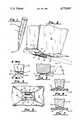
- FIG. 1is a perspective view of a preferred embodiment of an ultrasonic bonding tool incorporating the invention.
- FIG. 2is a perspective drawing of the tip of the tool of the invention, greatly enlarged, with a wire positioned in the channel as it would be for bonding.
- FIG. 3is a projective view of the tip normal to the axis of the channel.
- FIG. 4is a section of the tip shown in FIG. 3 perpendicular to the surface surrounding the channel of the preferred embodiment.
- FIG. 5is a projective view of the tip surface showing the true shape of the two flat surfaces surrounding and parallel to the axis of the channel therein.
- FIGS. 3-5are spatially oriented on the paper as projections from each other.
- FIG. 6is a section view of the tip normal to the axis of the channel showing the wire to be bonded and the pad to which the wire is to be bonded correctly positioned to commence bonding.
- FIG. 7is a section view of the tip normal to the axis of the channel and through a bond just after creating it using the wire shown in FIG. 6.
- FIG. 1shows the tip of the tool of the invention much magnified.
- the inventionhas been successfully used to bond 2.3 mil (0.584 mm.) O. D. wire.
- the principles involved and explained hereinare of general application for bonding a variety of wire sizes.
- FIG. 1the tool 10 for implementing the improved ultrasonic bonding process is shown greatly enlarged.
- One actual embodiment of tool 10has an overall length of less than 0.5 inch (1.3 cm.) and is used with a 2.3 mil (0.0584 mm.) O. D. wire (by way of comparison, less than the diameter of a human hair).
- Tool 10has a shank 11 which tapers to the tip 12 where the invention is embodied.
- the circle surrounding the tip 12 and the lead lineindicates that the tip 12 is shown further enlarged in FIGS. 2-7.
- FIG. 2The greatly enlarged perspective view of tip 12 in FIG. 2 shows the features of the invention with a wire 13 shown in outline positioned as it should be relative to the channel of the invention at the start of a bonding operation.
- FIGS. 3-5show projective views of the tip, further clarifying its geometry. The views of FIGS. 3-5 are spatially related to each other in that they are projections from each other as shown.
- Channel 21has a compound, curved cylindrical shape comprising a central concave surface 14 whose cross-sectional shape approximates a minor portion of the cross section of the wire to be bonded.
- minor portion of the cross sectionis to be interpreted to mean that less than half of the periphery's cross section is engaged with or abuts channel 14.
- surface 14is a portion of a circular cylinder subtending less than 180 degrees.
- the term “approximates”is used to accomodate the well-known requirement that a slight interference fit is necessary between the wire when positioned in the channel at the start of bonding to assure good mechanical connection between tool 10 and wire 13. This assures efficient transmission of the motion of tool 10 to wire 13 so that it is vibrated strongly against the pad 23 (see discussion for FIGS. 6 and 7) to which the wire 13 is to be bonded.
- a last definition neededis for the term "cylindrical” which in this context indicates that channel 21 has an invariant cross section over at least a part of its length, L as shown in FIGS. 2 and 4.
- the channel 21further comprises a pair of peripheral, nonconvex surfaces 15 and 16 each of which intersect an edge of central surface 14.
- Surfaces 15 and 16may have a finite radius of curvature somewhat larger than that of the central surface 14, or may be flat planes.
- the total area of the channel cross section, i.e. the area in FIG. 3 bounded by the peripheral surfaces 15 and 16, central surface 14, and dashed line 22 across the mouth of channel 21must be less than the cross-sectional area of the wire, but preferably at least 50%-70% of this area. This is so that flat surfaces 19 and 20 will not contact the pad 23 when bonding has been completed. (Note the clearance between pad 23 and surfaces 19 and 20 shown in FIG. 7.)
- the combination of a concave central surface 12 and nonconvex peripheral surfaces 15 and 16is what is meant by the term "compound, curved cylindrical surface".
- Beveled surfaces 17 and 18provide a smooth transition for the wire 13 from the bond area to the undistorted. While the bevel angle shown is 30 degrees (interior included angle of 150 degrees) which is preferred, other angles may work better for other sizes of wires and other aspects of the bonding operation. In certain circumstances, the beveled surfaces may be curved and blend smoothly with channel 21 and flat surfaces 19 and 20.
- tool 10is clamped by a set screw or other means in the chuck of a conventional ultrasonic bonding machine.
- Each wire 13 to be bondedis positioned in the channel as shown in FIGS. 2 and 6, and the bonding machine is caused to press the wire 13 firmly against pad 23 while vibrating tool 10 either transversely or along the wire's length. This is believed to generate heat which causes the wire 13 to fuse with pad 23.
- the wire 13is molded to a cross section as shown in FIG. 7.
- One reason that superior bond strength results from using a tool 10 with a tip 12 having the channel 14is that a greater bond area results.
- the nonconvex shape of peripheral surfaces 15 and 16molds the wire 13 into a shape whose bond characteristics are strong and reliably reproduceable.
- wire shape 13a shown in FIG. 7has a cross-sectional area essentially identical to that of the wire 13 before bonding shown in FIG. 6. That is, wire 13 undergoes no volumetric compression during the operation, nor is any wire material extruded from beneath tip 12.
- this toolalso increases the pressure between the wire and the pad during the bonding process because the peripheral channels 15 and 16 limit the spreading of the wire 13 during bonding. This is because the area of the footprint of the wire 13 on the pad is kept as small as possible by the peripheral channels 15 and 16. Furthermore, the footprint area is very consistent from one bond to the next even though there are unavoidable small variations in the time for the bonding operation and the force with which the tool presses the wire on the pad. Accordingly, I have found that use of this tool provides substantial advantages over these prior art bonding tools.
Landscapes
- Engineering & Computer Science (AREA)
- Mechanical Engineering (AREA)
- Manufacturing & Machinery (AREA)
- Computer Hardware Design (AREA)
- Microelectronics & Electronic Packaging (AREA)
- Power Engineering (AREA)
- Wire Bonding (AREA)
Abstract
Description
Claims (15)
Priority Applications (1)
| Application Number | Priority Date | Filing Date | Title |
|---|---|---|---|
| US06/938,178US4778097A (en) | 1986-12-04 | 1986-12-04 | Ultrasonic wire bonding tool |
Applications Claiming Priority (1)
| Application Number | Priority Date | Filing Date | Title |
|---|---|---|---|
| US06/938,178US4778097A (en) | 1986-12-04 | 1986-12-04 | Ultrasonic wire bonding tool |
Publications (1)
| Publication Number | Publication Date |
|---|---|
| US4778097Atrue US4778097A (en) | 1988-10-18 |
Family
ID=25471022
Family Applications (1)
| Application Number | Title | Priority Date | Filing Date |
|---|---|---|---|
| US06/938,178Expired - LifetimeUS4778097A (en) | 1986-12-04 | 1986-12-04 | Ultrasonic wire bonding tool |
Country Status (1)
| Country | Link |
|---|---|
| US (1) | US4778097A (en) |
Cited By (29)
| Publication number | Priority date | Publication date | Assignee | Title |
|---|---|---|---|---|
| US5079070A (en)* | 1990-10-11 | 1992-01-07 | International Business Machines Corporation | Repair of open defects in thin film conductors |
| US5193732A (en)* | 1991-10-04 | 1993-03-16 | International Business Machines Corporation | Apparatus and methods for making simultaneous electrical connections |
| US5240166A (en)* | 1992-05-15 | 1993-08-31 | International Business Machines Corporation | Device for thermally enhanced ultrasonic bonding with localized heat pulses |
| US5288007A (en)* | 1991-10-04 | 1994-02-22 | International Business Machine Corporation | Apparatus and methods for making simultaneous electrical connections |
| US5445306A (en)* | 1994-05-31 | 1995-08-29 | Motorola, Inc. | Wedge wire bonding tool tip |
| US5503321A (en)* | 1993-10-07 | 1996-04-02 | Nec Corporation | Bonding tool employed in ultrasonic compression bonding apparatus |
| US5647528A (en)* | 1996-02-06 | 1997-07-15 | Micron Technology, Inc. | Bondhead lead clamp apparatus and method |
| WO1997028922A1 (en)* | 1996-02-12 | 1997-08-14 | Daimler-Benz Aktiengesellschaft | Method of bonding insulating wire and device for carrying out this method |
| US5954842A (en)* | 1996-01-26 | 1999-09-21 | Micron Technology, Inc. | Lead finger clamp assembly |
| US5954260A (en)* | 1996-12-17 | 1999-09-21 | Texas Instruments Incorporated | Fine pitch bonding technique |
| US6068174A (en)* | 1996-12-13 | 2000-05-30 | Micro)N Technology, Inc. | Device and method for clamping and wire-bonding the leads of a lead frame one set at a time |
| US6105846A (en)* | 1998-04-02 | 2000-08-22 | Micron Technology, Inc. | Non-conductive and self-leveling leadframe clamp insert for wirebonding integrated circuits |
| US6155474A (en)* | 1997-12-16 | 2000-12-05 | Texas Instruments Incorporated | Fine pitch bonding technique |
| US6158647A (en)* | 1998-09-29 | 2000-12-12 | Micron Technology, Inc. | Concave face wire bond capillary |
| US6162662A (en)* | 1998-02-23 | 2000-12-19 | Micron Technology, Inc. | Die paddle clamping method for wire bond enhancement |
| US20020048846A1 (en)* | 1998-12-11 | 2002-04-25 | Corisis David J. | Die paddle clamping method for wire bond enhancement |
| US6484922B2 (en) | 1996-01-26 | 2002-11-26 | Micron Technology, Inc. | Apparatus and method of clamping semiconductor devices using sliding finger supports |
| US6634538B2 (en) | 1998-04-02 | 2003-10-21 | Micron Technology, Inc. | Non-conductive and self-leveling leadframe clamp insert for wirebonding integrated circuits |
| US20040026483A1 (en)* | 1996-06-17 | 2004-02-12 | Ball Michael B. | Methods for lead penetrating clamping system |
| US20050087585A1 (en)* | 2003-10-23 | 2005-04-28 | Copperthite Theodore J. | Automated filament attachment system for vacuum fluorescent display |
| US20110204126A1 (en)* | 2010-02-23 | 2011-08-25 | Schott Solar Ag | Method and apparatus for applying solder to a work piece |
| US20110235681A1 (en)* | 2008-10-17 | 2011-09-29 | Ghassem Azdasht | Device for Positioning and Contacting Test Contacts |
| US20140377118A1 (en)* | 2006-05-23 | 2014-12-25 | Federal-Mogul Corporation | Powder metal ultrasonic welding tool and method of manufacture thereof |
| CN107685189A (en)* | 2016-08-04 | 2018-02-13 | 通用汽车环球科技运作有限责任公司 | Vibration welding system and method |
| CN108080781A (en)* | 2016-11-23 | 2018-05-29 | 通用汽车环球科技运作有限责任公司 | For the loudspeaker of ultrasonic welding process |
| US20180361421A1 (en)* | 2017-06-16 | 2018-12-20 | Fenghua Weilder Electric Appliance Co., Ltd. | Heating device for hot melt glue gun |
| US20210111146A1 (en)* | 2019-10-10 | 2021-04-15 | Skyworks Solutions, Inc. | Cupd wire bond capillary design |
| US11121114B2 (en)* | 2017-09-15 | 2021-09-14 | Fuji Electric Co., Ltd. | Wire bonding tool including a wedge tool |
| US11351622B2 (en)* | 2014-02-13 | 2022-06-07 | Te Connectivity Corporation | Laser soldering system |
Citations (8)
| Publication number | Priority date | Publication date | Assignee | Title |
|---|---|---|---|---|
| US3593906A (en)* | 1969-02-20 | 1971-07-20 | Ibm | Conductor handling and bonding system |
| US3711341A (en)* | 1970-05-04 | 1973-01-16 | Ibm | Method of making sintered metal ultrasonic bonding tips |
| US3934783A (en)* | 1974-09-30 | 1976-01-27 | Larrison John E | Multiface wire bonding method and tool |
| US3971499A (en)* | 1974-09-03 | 1976-07-27 | Tribotech | Bonding tool |
| US4030657A (en)* | 1972-12-26 | 1977-06-21 | Rca Corporation | Wire lead bonding tool |
| US4063673A (en)* | 1974-07-01 | 1977-12-20 | Motorola, Inc. | Ultrasonic bonding head |
| JPS5596643A (en)* | 1979-01-17 | 1980-07-23 | Toshiba Corp | Tip for bonding wire |
| JPS55151344A (en)* | 1979-05-16 | 1980-11-25 | Toshiba Corp | Wire bonding process |
- 1986
- 1986-12-04USUS06/938,178patent/US4778097A/ennot_activeExpired - Lifetime
Patent Citations (8)
| Publication number | Priority date | Publication date | Assignee | Title |
|---|---|---|---|---|
| US3593906A (en)* | 1969-02-20 | 1971-07-20 | Ibm | Conductor handling and bonding system |
| US3711341A (en)* | 1970-05-04 | 1973-01-16 | Ibm | Method of making sintered metal ultrasonic bonding tips |
| US4030657A (en)* | 1972-12-26 | 1977-06-21 | Rca Corporation | Wire lead bonding tool |
| US4063673A (en)* | 1974-07-01 | 1977-12-20 | Motorola, Inc. | Ultrasonic bonding head |
| US3971499A (en)* | 1974-09-03 | 1976-07-27 | Tribotech | Bonding tool |
| US3934783A (en)* | 1974-09-30 | 1976-01-27 | Larrison John E | Multiface wire bonding method and tool |
| JPS5596643A (en)* | 1979-01-17 | 1980-07-23 | Toshiba Corp | Tip for bonding wire |
| JPS55151344A (en)* | 1979-05-16 | 1980-11-25 | Toshiba Corp | Wire bonding process |
Non-Patent Citations (2)
| Title |
|---|
| "Ultrasonic Bonding Tools", Jan. 1985. |
| Ultrasonic Bonding Tools , Jan. 1985.* |
Cited By (84)
| Publication number | Priority date | Publication date | Assignee | Title |
|---|---|---|---|---|
| US5079070A (en)* | 1990-10-11 | 1992-01-07 | International Business Machines Corporation | Repair of open defects in thin film conductors |
| US5193732A (en)* | 1991-10-04 | 1993-03-16 | International Business Machines Corporation | Apparatus and methods for making simultaneous electrical connections |
| US5288007A (en)* | 1991-10-04 | 1994-02-22 | International Business Machine Corporation | Apparatus and methods for making simultaneous electrical connections |
| US5240166A (en)* | 1992-05-15 | 1993-08-31 | International Business Machines Corporation | Device for thermally enhanced ultrasonic bonding with localized heat pulses |
| US5503321A (en)* | 1993-10-07 | 1996-04-02 | Nec Corporation | Bonding tool employed in ultrasonic compression bonding apparatus |
| US5445306A (en)* | 1994-05-31 | 1995-08-29 | Motorola, Inc. | Wedge wire bonding tool tip |
| US20040035913A1 (en)* | 1996-01-26 | 2004-02-26 | Ball Michael B. | Apparatus of clamping semiconductor devices using sliding finger supports |
| US6715659B2 (en) | 1996-01-26 | 2004-04-06 | Micron Technology, Inc. | Apparatus for clamping semiconductor devices using sliding finger supports |
| US5954842A (en)* | 1996-01-26 | 1999-09-21 | Micron Technology, Inc. | Lead finger clamp assembly |
| US6484922B2 (en) | 1996-01-26 | 2002-11-26 | Micron Technology, Inc. | Apparatus and method of clamping semiconductor devices using sliding finger supports |
| US6637636B2 (en) | 1996-01-26 | 2003-10-28 | Micron Technology, Inc. | Apparatus of clamping semiconductor devices using sliding finger supports |
| US6047468A (en)* | 1996-01-26 | 2000-04-11 | Micron Technology, Inc. | Lead finger clamp assembly and method of stabilizing lead frame elements |
| US20060157532A1 (en)* | 1996-01-26 | 2006-07-20 | Ball Michael B | Apparatus of clamping semiconductor devices using sliding finger supports |
| US6981629B2 (en) | 1996-01-26 | 2006-01-03 | Micron Technology, Inc. | Apparatus of clamping semiconductor devices using sliding finger supports |
| US6325275B1 (en) | 1996-02-06 | 2001-12-04 | Micron Technology, Inc. | Bondhead lead clamp apparatus and method |
| US6837418B2 (en) | 1996-02-06 | 2005-01-04 | Micron Technology, Inc. | Bondhead lead clamp apparatus and method |
| US20040065719A1 (en)* | 1996-02-06 | 2004-04-08 | Ball Michael B. | Bondhead lead clamp apparatus and method |
| US6435400B1 (en) | 1996-02-06 | 2002-08-20 | Micron Technology, Inc. | Bondhead lead clamp apparatus and method |
| US20040026478A1 (en)* | 1996-02-06 | 2004-02-12 | Ball Michael B. | Bondhead lead clamp apparatus |
| US6290116B1 (en) | 1996-02-06 | 2001-09-18 | Micron Technology, Inc. | Bondhead lead clamp apparatus and method |
| US6662993B2 (en) | 1996-02-06 | 2003-12-16 | Micron Technology, Inc. | Bondhead lead clamp apparatus |
| US6000599A (en)* | 1996-02-06 | 1999-12-14 | Micron Technology, Inc. | Bondhead lead clamp apparatus and method |
| US6845898B2 (en) | 1996-02-06 | 2005-01-25 | Micron Technology, Inc. | Bondhead lead clamp apparatus |
| US6604671B2 (en) | 1996-02-06 | 2003-08-12 | Micron Technology, Inc. | Bondhead lead clamp apparatus and method |
| US5647528A (en)* | 1996-02-06 | 1997-07-15 | Micron Technology, Inc. | Bondhead lead clamp apparatus and method |
| US6464123B2 (en) | 1996-02-06 | 2002-10-15 | Micron Technology, Inc. | Bondhead lead clamp apparatus and method |
| WO1997028922A1 (en)* | 1996-02-12 | 1997-08-14 | Daimler-Benz Aktiengesellschaft | Method of bonding insulating wire and device for carrying out this method |
| US7131568B2 (en) | 1996-06-17 | 2006-11-07 | Micron Technology, Inc. | Methods for lead penetrating clamping system |
| US20040026483A1 (en)* | 1996-06-17 | 2004-02-12 | Ball Michael B. | Methods for lead penetrating clamping system |
| US6068174A (en)* | 1996-12-13 | 2000-05-30 | Micro)N Technology, Inc. | Device and method for clamping and wire-bonding the leads of a lead frame one set at a time |
| US6886734B2 (en) | 1996-12-13 | 2005-05-03 | Micron Technology, Inc. | Device and method for clamping and wire-bonding the leads of a lead frame one set at a time |
| US6467672B2 (en) | 1996-12-13 | 2002-10-22 | Micron Technology, Inc. | Methods for clamping and wire-bonding the leads of a lead frame one set at a time |
| US6478211B2 (en) | 1996-12-13 | 2002-11-12 | Micron Technology, Inc. | Device and method for clamping and wire-bonding the leads of a lead frame one set at a time |
| US6334566B1 (en) | 1996-12-13 | 2002-01-01 | Micron Technology | Device and method for clamping and wire-bonding the leads of a lead frame one set at a time |
| US20020179691A1 (en)* | 1996-12-13 | 2002-12-05 | Ball Michael B. | Device and method for clamping and wire-bonding the leads of a lead frame one set at a time |
| US6299049B1 (en) | 1996-12-13 | 2001-10-09 | Micron Technology, Inc. | Device and method for clamping and wire-bonding the leads of a lead frame one set at a time |
| US6786387B2 (en) | 1996-12-13 | 2004-09-07 | Micron Technology, Inc. | Method for clamping and wire-bonding the leads of a lead frame one set at a time |
| US5954260A (en)* | 1996-12-17 | 1999-09-21 | Texas Instruments Incorporated | Fine pitch bonding technique |
| US6155474A (en)* | 1997-12-16 | 2000-12-05 | Texas Instruments Incorporated | Fine pitch bonding technique |
| US6326238B1 (en) | 1998-02-23 | 2001-12-04 | Micron Technology, Inc. | Die paddle clamping method for wire bond enhancement |
| US6756659B2 (en) | 1998-02-23 | 2004-06-29 | Micron Technology, Inc. | Die paddle clamping method for wire bond enhancement |
| US6162662A (en)* | 1998-02-23 | 2000-12-19 | Micron Technology, Inc. | Die paddle clamping method for wire bond enhancement |
| US6507094B2 (en) | 1998-02-23 | 2003-01-14 | Micron Technology, Inc. | Die paddle clamping for wire bond enhancement |
| US6288441B1 (en) | 1998-02-23 | 2001-09-11 | Micron Technology, Inc. | Die paddle clamping method for wire bond enhancement |
| US6921017B2 (en) | 1998-04-02 | 2005-07-26 | Micron Technology, Inc. | Non-conductive and self-leveling leadframe clamp insert for wirebonding integrated circuits |
| US6126062A (en)* | 1998-04-02 | 2000-10-03 | Micron Technology, Inc. | Non-conductive and self-leveling leadframe clamp insert for wirebonding integrated circuits |
| US6375061B1 (en) | 1998-04-02 | 2002-04-23 | Micron Technology, Inc. | Non-conductive and self-leveling leadframe clamp insert for wirebonding integrated circuits |
| US6105846A (en)* | 1998-04-02 | 2000-08-22 | Micron Technology, Inc. | Non-conductive and self-leveling leadframe clamp insert for wirebonding integrated circuits |
| US6352191B1 (en) | 1998-04-02 | 2002-03-05 | Micron Technology, Inc. | Non-conductive and self-leveling leadframe clamp insert for wirebonding integrated circuits |
| US6634538B2 (en) | 1998-04-02 | 2003-10-21 | Micron Technology, Inc. | Non-conductive and self-leveling leadframe clamp insert for wirebonding integrated circuits |
| US20040026486A1 (en)* | 1998-04-02 | 2004-02-12 | Sven Evers | Non-conductive and self-leveling leadframe clamp insert for wirebonding integrated circuits |
| US6588649B2 (en) | 1998-04-02 | 2003-07-08 | Micron Technology, Inc. | Non-conductive and self-leveling leadframe clamp insert for wirebonding integrated circuits |
| US6138891A (en)* | 1998-04-02 | 2000-10-31 | Micron Technology, Inc. | Non-conductive and self-leveling leadframe clamp insert for wirebonding integrated circuits |
| US6595406B2 (en) | 1998-09-29 | 2003-07-22 | Micron Technology, Inc. | Concave face wire bond capillary and method |
| US20080302862A1 (en)* | 1998-09-29 | 2008-12-11 | Micron Technology, Inc. | Concave face wire bond capillary and method |
| US6158647A (en)* | 1998-09-29 | 2000-12-12 | Micron Technology, Inc. | Concave face wire bond capillary |
| US6966480B2 (en) | 1998-09-29 | 2005-11-22 | Micron Technology, Inc. | Concave face wire bond capillary and method |
| US20040056072A1 (en)* | 1998-09-29 | 2004-03-25 | Chapman Gregory M. | Concave face wire bond capillary and method |
| US20060032888A1 (en)* | 1998-09-29 | 2006-02-16 | Chapman Gregory M | Concave face wire bond capillary and method |
| US6439450B1 (en) | 1998-09-29 | 2002-08-27 | Micron Technology, Inc. | Concave face wire bond capillary |
| US6311890B1 (en) | 1998-09-29 | 2001-11-06 | Micron Technology, Inc. | Concave face wire bond capillary |
| US7677429B2 (en) | 1998-09-29 | 2010-03-16 | Micron Technology, Inc. | Concave face wire bond capillary and method |
| US7416107B2 (en) | 1998-09-29 | 2008-08-26 | Micron Technology, Inc. | Concave face wire bond capillary and method |
| US20020048846A1 (en)* | 1998-12-11 | 2002-04-25 | Corisis David J. | Die paddle clamping method for wire bond enhancement |
| US6977214B2 (en) | 1998-12-11 | 2005-12-20 | Micron Technology, Inc. | Die paddle clamping method for wire bond enhancement |
| US20060154404A1 (en)* | 1998-12-11 | 2006-07-13 | Corisis David J | Die paddle clamping method for wire bond enhancement |
| US20050087585A1 (en)* | 2003-10-23 | 2005-04-28 | Copperthite Theodore J. | Automated filament attachment system for vacuum fluorescent display |
| US7407079B2 (en)* | 2003-10-23 | 2008-08-05 | Orthodyne Electronics Corporation | Automated filament attachment system for vacuum fluorescent display |
| US20140377118A1 (en)* | 2006-05-23 | 2014-12-25 | Federal-Mogul Corporation | Powder metal ultrasonic welding tool and method of manufacture thereof |
| US9302323B2 (en)* | 2006-05-23 | 2016-04-05 | Federal-Mogul Corporation | Powder metal ultrasonic welding tool and method of manufacture thereof |
| US20110235681A1 (en)* | 2008-10-17 | 2011-09-29 | Ghassem Azdasht | Device for Positioning and Contacting Test Contacts |
| US8480298B2 (en)* | 2008-10-17 | 2013-07-09 | PAC Tech—Packaging Technologies GmbH | Device for positioning and contacting test contacts |
| US20110204126A1 (en)* | 2010-02-23 | 2011-08-25 | Schott Solar Ag | Method and apparatus for applying solder to a work piece |
| US20140158749A1 (en)* | 2010-02-23 | 2014-06-12 | Hilmar von Campe | Method and apparatus for applying solder to a work piece |
| US8777087B2 (en)* | 2010-02-23 | 2014-07-15 | Schott Solar Ag | Method and apparatus for applying solder to a work piece |
| US11351622B2 (en)* | 2014-02-13 | 2022-06-07 | Te Connectivity Corporation | Laser soldering system |
| CN107685189A (en)* | 2016-08-04 | 2018-02-13 | 通用汽车环球科技运作有限责任公司 | Vibration welding system and method |
| CN107685189B (en)* | 2016-08-04 | 2020-07-03 | 通用汽车环球科技运作有限责任公司 | Vibration welding system and method |
| CN108080781A (en)* | 2016-11-23 | 2018-05-29 | 通用汽车环球科技运作有限责任公司 | For the loudspeaker of ultrasonic welding process |
| US20180361421A1 (en)* | 2017-06-16 | 2018-12-20 | Fenghua Weilder Electric Appliance Co., Ltd. | Heating device for hot melt glue gun |
| US11813638B2 (en)* | 2017-06-16 | 2023-11-14 | Ningbo Weilder Electric Appliance Co., Ltd. | Heating device for hot melt glue gun |
| US11121114B2 (en)* | 2017-09-15 | 2021-09-14 | Fuji Electric Co., Ltd. | Wire bonding tool including a wedge tool |
| US20210111146A1 (en)* | 2019-10-10 | 2021-04-15 | Skyworks Solutions, Inc. | Cupd wire bond capillary design |
| US12308341B2 (en)* | 2019-10-10 | 2025-05-20 | Skyworks Solutions, Inc. | Wire bond capillary design |
Similar Documents
| Publication | Publication Date | Title |
|---|---|---|
| US4778097A (en) | Ultrasonic wire bonding tool | |
| US3623649A (en) | Wedge bonding tool for the attachment of semiconductor leads | |
| US7416107B2 (en) | Concave face wire bond capillary and method | |
| US3203078A (en) | Method of making an electrical connection | |
| JP6574795B2 (en) | Manufacturing method of electric wire with terminal | |
| US11791599B2 (en) | Electric cable with terminal and method for manufacturing electric cable with terminal | |
| CN110718778A (en) | Wire with terminal and method of making the same | |
| US5899769A (en) | Device for connecting a coaxial cable to contacts which can be connected to extension lead arrangements | |
| CA2042746C (en) | Crimping tool having improved crimping dies | |
| US20240178581A1 (en) | Connection structure between terminal and electric wire | |
| JPH07161448A (en) | Manufacture of crimp terminal | |
| US2707824A (en) | Method of making cold-weld joints | |
| JP7074109B2 (en) | Coil parts and their manufacturing methods | |
| JP4132792B2 (en) | Capillary structure used for wire bonding | |
| JP3732657B2 (en) | Covered wire connection method and connection structure | |
| JP7723732B2 (en) | Wire Bonding Capillary | |
| JP3381910B2 (en) | Wire bonding equipment | |
| JP3067615B2 (en) | Planar commutator | |
| JP4194317B2 (en) | Coining punch for lead frame processing and manufacturing method of coining punch | |
| WO2019049440A1 (en) | Method for manufacturing spark plug | |
| JP2872469B2 (en) | Manufacturing method of sliding contact | |
| JPH05166688A (en) | Manufacture of lead for electrolytic capacitor | |
| JPH0529064A (en) | Manufacture of spark plug | |
| JPH0779118B2 (en) | Wire bonding equipment | |
| GB2110128A (en) | Electrical connector terminal for use in the connector and method of producing same |
Legal Events
| Date | Code | Title | Description |
|---|---|---|---|
| AS | Assignment | Owner name:MAGNETIC PERIPHERALS INC., C/O CONTROL DATA CORPOR Free format text:ASSIGNMENT OF ASSIGNORS INTEREST.;ASSIGNOR:HAUSER, JOHN G.;REEL/FRAME:004694/0782 Effective date:19870205 | |
| STCF | Information on status: patent grant | Free format text:PATENTED CASE | |
| AS | Assignment | Owner name:SECURITY PACIFIC NATIONAL BANK, AS AGENT, NEW YORK Free format text:SECURITY INTEREST;ASSIGNOR:MAGNETIC PERIPHERALS, INC.;REEL/FRAME:005184/0213 Effective date:19890929 | |
| FPAY | Fee payment | Year of fee payment:4 | |
| FEPP | Fee payment procedure | Free format text:PAYOR NUMBER ASSIGNED (ORIGINAL EVENT CODE: ASPN); ENTITY STATUS OF PATENT OWNER: LARGE ENTITY | |
| AS | Assignment | Owner name:SEAGATE TECHNOLOGY, INC., CALIFORNIA Free format text:MERGER;ASSIGNOR:MAGNETIC PHERIPHERALS INC.;REEL/FRAME:006486/0237 Effective date:19900531 | |
| AS | Assignment | Owner name:SEAGATE TECHNOLOGY, INC., CALIFORNIA Free format text:RELEASED BY SECURED PARTY;ASSIGNOR:BANKAMERICA;REEL/FRAME:006518/0887 Effective date:19930128 | |
| FEPP | Fee payment procedure | Free format text:PAYER NUMBER DE-ASSIGNED (ORIGINAL EVENT CODE: RMPN); ENTITY STATUS OF PATENT OWNER: LARGE ENTITY Free format text:PAYOR NUMBER ASSIGNED (ORIGINAL EVENT CODE: ASPN); ENTITY STATUS OF PATENT OWNER: LARGE ENTITY | |
| FPAY | Fee payment | Year of fee payment:8 | |
| FPAY | Fee payment | Year of fee payment:12 | |
| AS | Assignment | Owner name:SEAGATE TECHNOLOGY LLC, CALIFORNIA Free format text:ASSIGNMENT OF ASSIGNORS INTEREST;ASSIGNOR:SEAGATE TECHNOLOGY, INC.;REEL/FRAME:011077/0319 Effective date:20000728 | |
| AS | Assignment | Owner name:THE CHASE MANHATTAN BANK, AS COLLATERAL AGENT, NEW Free format text:SECURITY AGREEMENT;ASSIGNOR:SEAGATE TECHNOLOGY LLC;REEL/FRAME:011461/0001 Effective date:20001122 | |
| AS | Assignment | Owner name:JPMORGAN CHASE BANK, AS COLLATERAL AGENT, NEW YORK Free format text:SECURITY AGREEMENT;ASSIGNOR:SEAGATE TECHNOLOGY LLC;REEL/FRAME:013177/0001 Effective date:20020513 Owner name:JPMORGAN CHASE BANK, AS COLLATERAL AGENT,NEW YORK Free format text:SECURITY AGREEMENT;ASSIGNOR:SEAGATE TECHNOLOGY LLC;REEL/FRAME:013177/0001 Effective date:20020513 | |
| AS | Assignment | Owner name:SEAGATE TECHNOLOGY LLC, CALIFORNIA Free format text:RELEASE OF SECURITY INTERESTS IN PATENT RIGHTS;ASSIGNOR:JPMORGAN CHASE BANK, N.A. (FORMERLY KNOWN AS THE CHASE MANHATTAN BANK AND JPMORGAN CHASE BANK), AS ADMINISTRATIVE AGENT;REEL/FRAME:016926/0821 Effective date:20051130 |