US4772571A - Process of self aligned nitridation of TiSi2 to form TiN/TiSi2 contact - Google Patents
Process of self aligned nitridation of TiSi2 to form TiN/TiSi2 contactDownload PDFInfo
- Publication number
- US4772571A US4772571AUS07/050,467US5046787AUS4772571AUS 4772571 AUS4772571 AUS 4772571AUS 5046787 AUS5046787 AUS 5046787AUS 4772571 AUS4772571 AUS 4772571A
- Authority
- US
- United States
- Prior art keywords
- wafer
- titanium
- titanium nitride
- disilicide
- nitrogen
- Prior art date
- Legal status (The legal status is an assumption and is not a legal conclusion. Google has not performed a legal analysis and makes no representation as to the accuracy of the status listed.)
- Expired - Lifetime
Links
Images
Classifications
- H—ELECTRICITY
- H01—ELECTRIC ELEMENTS
- H01L—SEMICONDUCTOR DEVICES NOT COVERED BY CLASS H10
- H01L21/00—Processes or apparatus adapted for the manufacture or treatment of semiconductor or solid state devices or of parts thereof
- H01L21/70—Manufacture or treatment of devices consisting of a plurality of solid state components formed in or on a common substrate or of parts thereof; Manufacture of integrated circuit devices or of parts thereof
- H01L21/71—Manufacture of specific parts of devices defined in group H01L21/70
- H01L21/768—Applying interconnections to be used for carrying current between separate components within a device comprising conductors and dielectrics
- H01L21/76838—Applying interconnections to be used for carrying current between separate components within a device comprising conductors and dielectrics characterised by the formation and the after-treatment of the conductors
- H01L21/76886—Modifying permanently or temporarily the pattern or the conductivity of conductive members, e.g. formation of alloys, reduction of contact resistances
- H01L21/76889—Modifying permanently or temporarily the pattern or the conductivity of conductive members, e.g. formation of alloys, reduction of contact resistances by forming silicides of refractory metals
- H—ELECTRICITY
- H01—ELECTRIC ELEMENTS
- H01L—SEMICONDUCTOR DEVICES NOT COVERED BY CLASS H10
- H01L23/00—Details of semiconductor or other solid state devices
- H01L23/52—Arrangements for conducting electric current within the device in operation from one component to another, i.e. interconnections, e.g. wires, lead frames
- H01L23/522—Arrangements for conducting electric current within the device in operation from one component to another, i.e. interconnections, e.g. wires, lead frames including external interconnections consisting of a multilayer structure of conductive and insulating layers inseparably formed on the semiconductor body
- H01L23/532—Arrangements for conducting electric current within the device in operation from one component to another, i.e. interconnections, e.g. wires, lead frames including external interconnections consisting of a multilayer structure of conductive and insulating layers inseparably formed on the semiconductor body characterised by the materials
- H01L23/53204—Conductive materials
- H01L23/53209—Conductive materials based on metals, e.g. alloys, metal silicides
- H01L23/53257—Conductive materials based on metals, e.g. alloys, metal silicides the principal metal being a refractory metal
- H—ELECTRICITY
- H01—ELECTRIC ELEMENTS
- H01L—SEMICONDUCTOR DEVICES NOT COVERED BY CLASS H10
- H01L2924/00—Indexing scheme for arrangements or methods for connecting or disconnecting semiconductor or solid-state bodies as covered by H01L24/00
- H01L2924/0001—Technical content checked by a classifier
- H01L2924/0002—Not covered by any one of groups H01L24/00, H01L24/00 and H01L2224/00
- Y—GENERAL TAGGING OF NEW TECHNOLOGICAL DEVELOPMENTS; GENERAL TAGGING OF CROSS-SECTIONAL TECHNOLOGIES SPANNING OVER SEVERAL SECTIONS OF THE IPC; TECHNICAL SUBJECTS COVERED BY FORMER USPC CROSS-REFERENCE ART COLLECTIONS [XRACs] AND DIGESTS
- Y10—TECHNICAL SUBJECTS COVERED BY FORMER USPC
- Y10S—TECHNICAL SUBJECTS COVERED BY FORMER USPC CROSS-REFERENCE ART COLLECTIONS [XRACs] AND DIGESTS
- Y10S148/00—Metal treatment
- Y10S148/019—Contacts of silicides
Definitions
- This inventionrelates to semiconductor devices and the manufacture thereof and, in particular, to semiconductor devices including silicides.
- Polysiliconhas conventionally been employed for gates and interconnections in integrated circuits. However, for small geometry, high speed integrated circuits it is desirable to use alternative materials with lower resistivity, such as metallic silicides.
- Our co-pending GB Applications No. 8328552(Ser. No. 2139420) (P. D. Scovell et al 5-3-2X) and No. 8312281 (Ser. No. 2139419 (P. D. Scovell et al 7-4-3) describe methods of forming metallic silicide elements.
- Titanium disilicideis now one of the most favoured replacements for heavily-doped polysilicon as an interconnect in MOS devices with geometries down to 1 ⁇ m. Titanium disilicide has numerous beneficial qualities. It is a refractory metal. It has the lowest thin film resistivity of any refractory silicide. It is readily etched. Metal over the silicide can be etched with great selectivity, and a high quality silicon dioxide layer can be grown over the silicide with no chance of forming volatile metal oxides.
- One significant disadvantage of this materialis that it does not form a barrier to silicon diffusion from beneath the silicide. Thus where aluminium is disposed over silicide, silicon can diffuse up into the aluminium where it can precipitate to form a high resistance layer, and this diffusion is a significant cause of device failure. It is an object of the present invention to overcome this disadvantage.
- a semiconductor deviceincluding a metallic silicide element and a metal element in electrical contact therewith via a nitrided region of the metallic silicide element.
- a method of manufacturing a semiconductor deviceincluding the steps of forming a metallic silicide element on a semiconductor wafer, providing an electrically insulating layer over the wafer, exposing a region of the metallic silicide element via a hole in the electrically insulating layer, annealing the wafer in nitrogen whereby to locally nitride the exposed metallic silicide region, metallising the wafer, and patterning the metallisation to form a metal element, the metallic silicide element being in electrical contact with the metal element via the locally nitrided metallic silicide region.
- a method of manufacturing a semiconductor deviceincluding the step of forming a titanium disilicide interconnect, locally nitriding a region of the interconnect and disposing an aluminium element in electrical contact with the nitrided region.
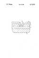
- the accompanying drawingshows a cross-section through part of a semiconductor device.
- Titanium nitrideis known to be a good barrier to silicon diffusion while still having an acceptably low resistivity. It is thus proposed to selectively form titanium nitride at points where electrical contact between aluminium metallisation and underlying titanium silicide is required.
- the silicideprovides a low resistivity interconnect while the nitride provides the ideal contact material to aluminium, having a low contact resistance and preventing silicon diffusing up into the aluminium.
- the titanium nitridecan be formed in a simple manner with only minimal disturbance to the conventional MOS Process.
- reference numeral 1indicates a titanium disilicide interconnect extending over a substrate 2 (wafer) including active components (not shown) of an integrated circuit.
- Such an interconnect 1is manufactured by forming a layer of titanium disilicide over the substrate 2 and subsequent patterning thereof. After patterning the silicide, a thick oxide (silicon dioxide) layer 3 is provided over the entire wafer. Holes such as 4 are then cut (etched) in layer 3 to expose the silicide 1.
- the processing steps outlined aboveare those of the normal MOS Process.
- the next stepwhich is not part of the normal MOS Process, comprises annealing the wafer in nitrogen. The nitrogen reacts with silicide exposed by the holes 4 to form titanium nitride regions (contacts) 5 thereat. The only exposed silicide is in the contact holes 4. Following this anneal, aluminium is deposited as in the normal MOS process, resulting in layer 5 which can be subsequently patterned as in the normal process.
- the annealing in nitrogenmay involve, for example, a temperature of 1000° C. for one hour, or alternatively 1100° C. for a few seconds. Both processes result in the formation of an adequate titanium nitride region 5.
- the method proposedinvolves selectively nitriding a low resistivity silicide interconnect by annealing it in nitrogen to form a low resistivity nitride region which forms a barrier to silicon diffusion.
- the process used to form the nitride layeris simple and achieves a truly self-aligned barrier.
Landscapes
- Engineering & Computer Science (AREA)
- Microelectronics & Electronic Packaging (AREA)
- Condensed Matter Physics & Semiconductors (AREA)
- General Physics & Mathematics (AREA)
- Computer Hardware Design (AREA)
- Physics & Mathematics (AREA)
- Power Engineering (AREA)
- Manufacturing & Machinery (AREA)
- Internal Circuitry In Semiconductor Integrated Circuit Devices (AREA)
- Electrodes Of Semiconductors (AREA)
- Bipolar Transistors (AREA)
- Heterocyclic Carbon Compounds Containing A Hetero Ring Having Oxygen Or Sulfur (AREA)
- Recrystallisation Techniques (AREA)
- Semiconductor Memories (AREA)
- Semiconductor Integrated Circuits (AREA)
Abstract
Description
Claims (6)
Applications Claiming Priority (2)
| Application Number | Priority Date | Filing Date | Title |
|---|---|---|---|
| GB8423265 | 1984-09-14 | ||
| GB08423265AGB2164491B (en) | 1984-09-14 | 1984-09-14 | Semiconductor devices |
Related Parent Applications (1)
| Application Number | Title | Priority Date | Filing Date |
|---|---|---|---|
| US06775529Division | 1985-09-13 |
Publications (1)
| Publication Number | Publication Date |
|---|---|
| US4772571Atrue US4772571A (en) | 1988-09-20 |
Family
ID=10566719
Family Applications (1)
| Application Number | Title | Priority Date | Filing Date |
|---|---|---|---|
| US07/050,467Expired - LifetimeUS4772571A (en) | 1984-09-14 | 1987-05-18 | Process of self aligned nitridation of TiSi2 to form TiN/TiSi2 contact |
Country Status (6)
| Country | Link |
|---|---|
| US (1) | US4772571A (en) |
| EP (1) | EP0174773B1 (en) |
| JP (1) | JPS6173370A (en) |
| AT (1) | ATE60853T1 (en) |
| DE (1) | DE3581682D1 (en) |
| GB (1) | GB2164491B (en) |
Cited By (35)
| Publication number | Priority date | Publication date | Assignee | Title |
|---|---|---|---|---|
| US4931411A (en)* | 1985-05-01 | 1990-06-05 | Texas Instruments Incorporated | Integrated circuit process with TiN-gate transistor |
| US5166771A (en)* | 1990-01-12 | 1992-11-24 | Paradigm Technology, Inc. | Self-aligning contact and interconnect structure |
| US5172211A (en)* | 1990-01-12 | 1992-12-15 | Paradigm Technology, Inc. | High resistance polysilicon load resistor |
| US5369302A (en)* | 1990-10-22 | 1994-11-29 | Sgs-Thomson Microelectronics, Inc. | Method to improve step coverage by contact reflow |
| US5371041A (en)* | 1988-02-11 | 1994-12-06 | Sgs-Thomson Microelectronics, Inc. | Method for forming a contact/VIA |
| US5374592A (en)* | 1992-09-22 | 1994-12-20 | Sgs-Thomson Microelectronics, Inc. | Method for forming an aluminum metal contact |
| US5389575A (en)* | 1991-07-12 | 1995-02-14 | Hughes Aircraft Company | Self-aligned contact diffusion barrier method |
| US5472912A (en)* | 1989-11-30 | 1995-12-05 | Sgs-Thomson Microelectronics, Inc. | Method of making an integrated circuit structure by using a non-conductive plug |
| US5512516A (en)* | 1988-05-27 | 1996-04-30 | Fujitsu Limited | Contact structure for connecting an electrode to a semiconductor device and a method of forming the same |
| US5652180A (en)* | 1993-06-28 | 1997-07-29 | Kawasaki Steel Corporation | Method of manufacturing semiconductor device with contact structure |
| US5656861A (en)* | 1990-01-12 | 1997-08-12 | Paradigm Technology, Inc. | Self-aligning contact and interconnect structure |
| US5658828A (en)* | 1989-11-30 | 1997-08-19 | Sgs-Thomson Microelectronics, Inc. | Method for forming an aluminum contact through an insulating layer |
| US5760475A (en)* | 1987-03-30 | 1998-06-02 | International Business Machines Corporation | Refractory metal-titanium nitride conductive structures |
| US5834846A (en)* | 1995-01-10 | 1998-11-10 | Kawasaki Steel Corporation | Semiconductor device with contact structure and method of manufacturing the same |
| US5930673A (en)* | 1990-11-05 | 1999-07-27 | Stmicroelectronics, Inc. | Method for forming a metal contact |
| US5956611A (en)* | 1997-09-03 | 1999-09-21 | Micron Technologies, Inc. | Field emission displays with reduced light leakage |
| US6001729A (en)* | 1995-01-10 | 1999-12-14 | Kawasaki Steel Corporation | Method of forming wiring structure for semiconductor device |
| US6242811B1 (en) | 1989-11-30 | 2001-06-05 | Stmicroelectronics, Inc. | Interlevel contact including aluminum-refractory metal alloy formed during aluminum deposition at an elevated temperature |
| US6271137B1 (en) | 1989-11-30 | 2001-08-07 | Stmicroelectronics, Inc. | Method of producing an aluminum stacked contact/via for multilayer |
| US6271120B1 (en)* | 1995-03-10 | 2001-08-07 | Advanced Micro Devices, Inc. | Method of enhanced silicide layer for advanced metal diffusion barrier layer application |
| US6287963B1 (en) | 1990-11-05 | 2001-09-11 | Stmicroelectronics, Inc. | Method for forming a metal contact |
| US6365488B1 (en)* | 1998-03-05 | 2002-04-02 | Industrial Technology Research Institute | Method of manufacturing SOI wafer with buried layer |
| US6579614B2 (en)* | 1999-06-22 | 2003-06-17 | International Business Machines Corporation | Structure having refractory metal film on a substrate |
| US6617242B1 (en)* | 1989-11-30 | 2003-09-09 | Stmicroelectronics, Inc. | Method for fabricating interlevel contacts of aluminum/refractory metal alloys |
| US20060250837A1 (en)* | 2005-05-09 | 2006-11-09 | Sandisk 3D, Llc | Nonvolatile memory cell comprising a diode and a resistance-switching material |
| US20070114509A1 (en)* | 2005-11-23 | 2007-05-24 | Sandisk 3D Llc | Memory cell comprising nickel-cobalt oxide switching element |
| US20070228354A1 (en)* | 2006-03-31 | 2007-10-04 | Sandisk 3D, Llc | Nonvolatile rewritable memory cell comprising a resistivity-switching oxide or nitride and an antifuse |
| US20070228414A1 (en)* | 2006-03-31 | 2007-10-04 | Sandisk 3D, Llc | Heterojunction device comprising a semiconductor and a resistivity-switching oxide or nitride |
| US20070236981A1 (en)* | 2006-03-31 | 2007-10-11 | Sandisk 3D, Llc | Multilevel nonvolatile memory cell comprising a resistivity-switching oxide or nitride and an antifuse |
| US20090001342A1 (en)* | 2007-06-29 | 2009-01-01 | April Schricker | Memory cell that employs a selectively grown reversible resistance-switching element and methods of forming the same |
| US20090001345A1 (en)* | 2007-06-29 | 2009-01-01 | April Schricker | Memory cell that employs a selectively deposited reversible resistance-switching element and methods of forming the same |
| US20090001344A1 (en)* | 2007-06-29 | 2009-01-01 | April Schricker | Memory cell that employs a selectively grown reversible resistance-switching element and methods of forming the same |
| US20090001343A1 (en)* | 2007-06-29 | 2009-01-01 | April Schricker | Memory cell that employs a selectively deposited reversible resistance-switching element and methods of forming the same |
| US20090104756A1 (en)* | 2007-06-29 | 2009-04-23 | Tanmay Kumar | Method to form a rewriteable memory cell comprising a diode and a resistivity-switching grown oxide |
| US20150303246A1 (en)* | 2014-04-16 | 2015-10-22 | Cirrus Logic, Inc. | Systems and methods for fabricating a polycrystaline semiconductor resistor on a semiconductor substrate |
Families Citing this family (7)
| Publication number | Priority date | Publication date | Assignee | Title |
|---|---|---|---|---|
| EP0194950B1 (en)* | 1985-03-15 | 1992-05-27 | Fairchild Semiconductor Corporation | High temperature interconnect system for an integrated circuit |
| US4920071A (en)* | 1985-03-15 | 1990-04-24 | Fairchild Camera And Instrument Corporation | High temperature interconnect system for an integrated circuit |
| JPS6358927A (en)* | 1986-08-29 | 1988-03-14 | Mitsubishi Electric Corp | Manufacturing method of semiconductor device |
| US4897287A (en)* | 1988-10-06 | 1990-01-30 | The Boc Group, Inc. | Metallization process for an integrated circuit |
| KR920005242A (en)* | 1990-08-20 | 1992-03-28 | 김광호 | Method of manufacturing transistor having structure of gate-insulator-semiconductor |
| JP2756886B2 (en)* | 1991-08-30 | 1998-05-25 | 三菱電機株式会社 | Semiconductor device and manufacturing method thereof |
| KR200465941Y1 (en)* | 2011-11-11 | 2013-03-19 | 박혜원 | Cushion sofa |
Citations (7)
| Publication number | Priority date | Publication date | Assignee | Title |
|---|---|---|---|---|
| US4468308A (en)* | 1982-02-04 | 1984-08-28 | Itt Industries, Inc. | Metallic silicide production |
| EP0127281A1 (en)* | 1983-03-25 | 1984-12-05 | Fujitsu Limited | An electrode for a semiconductor device |
| US4528744A (en)* | 1982-04-08 | 1985-07-16 | Tokyo Shibaura Denki Kabushiki Kaisha | Method of manufacturing a semiconductor device |
| US4545116A (en)* | 1983-05-06 | 1985-10-08 | Texas Instruments Incorporated | Method of forming a titanium disilicide |
| US4567058A (en)* | 1984-07-27 | 1986-01-28 | Fairchild Camera & Instrument Corporation | Method for controlling lateral diffusion of silicon in a self-aligned TiSi2 process |
| US4599196A (en)* | 1983-04-21 | 1986-07-08 | Commissariat A L'energie Atomique | Process for the conditioning of contaminated waste, particularly cation exchange materials |
| US4622735A (en)* | 1980-12-12 | 1986-11-18 | Tokyo Shibaura Denki Kabushiki Kaisha | Method for manufacturing a semiconductor device utilizing self-aligned silicide regions |
Family Cites Families (6)
| Publication number | Priority date | Publication date | Assignee | Title |
|---|---|---|---|---|
| US3701931A (en)* | 1971-05-06 | 1972-10-31 | Ibm | Gold tantalum-nitrogen high conductivity metallurgy |
| US3879746A (en)* | 1972-05-30 | 1975-04-22 | Bell Telephone Labor Inc | Gate metallization structure |
| US4332839A (en)* | 1978-12-29 | 1982-06-01 | Bell Telephone Laboratories, Incorporated | Method for making integrated semiconductor circuit structure with formation of Ti or Ta silicide |
| DE3027954A1 (en)* | 1980-07-23 | 1982-02-25 | Siemens AG, 1000 Berlin und 8000 München | MOS integrated circuit with supplementary wiring plane - of silicide of high melting metal completely independent of metal wiring plane |
| JPS58103168A (en)* | 1981-12-16 | 1983-06-20 | Fujitsu Ltd | semiconductor equipment |
| US4429011A (en)* | 1982-03-29 | 1984-01-31 | General Electric Company | Composite conductive structures and method of making same |
- 1984
- 1984-09-14GBGB08423265Apatent/GB2164491B/ennot_activeExpired
- 1985
- 1985-08-29ATAT85306106Tpatent/ATE60853T1/ennot_activeIP Right Cessation
- 1985-08-29DEDE8585306106Tpatent/DE3581682D1/ennot_activeExpired - Fee Related
- 1985-08-29EPEP85306106Apatent/EP0174773B1/ennot_activeExpired - Lifetime
- 1985-09-10JPJP60200390Apatent/JPS6173370A/enactivePending
- 1987
- 1987-05-18USUS07/050,467patent/US4772571A/ennot_activeExpired - Lifetime
Patent Citations (7)
| Publication number | Priority date | Publication date | Assignee | Title |
|---|---|---|---|---|
| US4622735A (en)* | 1980-12-12 | 1986-11-18 | Tokyo Shibaura Denki Kabushiki Kaisha | Method for manufacturing a semiconductor device utilizing self-aligned silicide regions |
| US4468308A (en)* | 1982-02-04 | 1984-08-28 | Itt Industries, Inc. | Metallic silicide production |
| US4528744A (en)* | 1982-04-08 | 1985-07-16 | Tokyo Shibaura Denki Kabushiki Kaisha | Method of manufacturing a semiconductor device |
| EP0127281A1 (en)* | 1983-03-25 | 1984-12-05 | Fujitsu Limited | An electrode for a semiconductor device |
| US4599196A (en)* | 1983-04-21 | 1986-07-08 | Commissariat A L'energie Atomique | Process for the conditioning of contaminated waste, particularly cation exchange materials |
| US4545116A (en)* | 1983-05-06 | 1985-10-08 | Texas Instruments Incorporated | Method of forming a titanium disilicide |
| US4567058A (en)* | 1984-07-27 | 1986-01-28 | Fairchild Camera & Instrument Corporation | Method for controlling lateral diffusion of silicon in a self-aligned TiSi2 process |
Non-Patent Citations (8)
| Title |
|---|
| C. Y. Ting and M. Wittmer, Thin Solid Films, 96 (1982), pp. 327 345.* |
| C. Y. Ting and M. Wittmer, Thin Solid Films, 96 (1982), pp. 327-345. |
| C. Y. Ting, J. Vac. Sci. Technol., 21 (1), May/Jun. 1982, pp. 14 18.* |
| C. Y. Ting, J. Vac. Sci. Technol., 21 (1), May/Jun. 1982, pp. 14-18. |
| M. A. Nicollet, Thin Solid Films, 52 (1978), pp. 415 445.* |
| M. A. Nicollet, Thin Solid Films, 52 (1978), pp. 415-445. |
| P. J. Rossez, G. J. Tomkins, "Self Aligned Nitridation of TiSi2 : a TiN/TiSi2 Contact Structure", Materials Res. Soc. Symp. Proc., vol. 37 (Gibson et al. ed.), pp. 607-612, 1985, Mat. Res. Soc. |
| P. J. Rossez, G. J. Tomkins, Self Aligned Nitridation of TiSi 2 : a TiN/TiSi 2 Contact Structure , Materials Res. Soc. Symp. Proc., vol. 37 (Gibson et al. ed.), pp. 607 612, 1985, Mat. Res. Soc.* |
Cited By (63)
| Publication number | Priority date | Publication date | Assignee | Title |
|---|---|---|---|---|
| US4931411A (en)* | 1985-05-01 | 1990-06-05 | Texas Instruments Incorporated | Integrated circuit process with TiN-gate transistor |
| US5760475A (en)* | 1987-03-30 | 1998-06-02 | International Business Machines Corporation | Refractory metal-titanium nitride conductive structures |
| US5371041A (en)* | 1988-02-11 | 1994-12-06 | Sgs-Thomson Microelectronics, Inc. | Method for forming a contact/VIA |
| US5512516A (en)* | 1988-05-27 | 1996-04-30 | Fujitsu Limited | Contact structure for connecting an electrode to a semiconductor device and a method of forming the same |
| US6617242B1 (en)* | 1989-11-30 | 2003-09-09 | Stmicroelectronics, Inc. | Method for fabricating interlevel contacts of aluminum/refractory metal alloys |
| US5976969A (en)* | 1989-11-30 | 1999-11-02 | Stmicroelectronics, Inc. | Method for forming an aluminum contact |
| US5472912A (en)* | 1989-11-30 | 1995-12-05 | Sgs-Thomson Microelectronics, Inc. | Method of making an integrated circuit structure by using a non-conductive plug |
| US6271137B1 (en) | 1989-11-30 | 2001-08-07 | Stmicroelectronics, Inc. | Method of producing an aluminum stacked contact/via for multilayer |
| US6242811B1 (en) | 1989-11-30 | 2001-06-05 | Stmicroelectronics, Inc. | Interlevel contact including aluminum-refractory metal alloy formed during aluminum deposition at an elevated temperature |
| US5658828A (en)* | 1989-11-30 | 1997-08-19 | Sgs-Thomson Microelectronics, Inc. | Method for forming an aluminum contact through an insulating layer |
| US5172211A (en)* | 1990-01-12 | 1992-12-15 | Paradigm Technology, Inc. | High resistance polysilicon load resistor |
| US5620919A (en)* | 1990-01-12 | 1997-04-15 | Paradigm Technology, Inc. | Methods for fabricating integrated circuits including openings to transistor regions |
| US5656861A (en)* | 1990-01-12 | 1997-08-12 | Paradigm Technology, Inc. | Self-aligning contact and interconnect structure |
| US5166771A (en)* | 1990-01-12 | 1992-11-24 | Paradigm Technology, Inc. | Self-aligning contact and interconnect structure |
| US5369302A (en)* | 1990-10-22 | 1994-11-29 | Sgs-Thomson Microelectronics, Inc. | Method to improve step coverage by contact reflow |
| US6287963B1 (en) | 1990-11-05 | 2001-09-11 | Stmicroelectronics, Inc. | Method for forming a metal contact |
| US5930673A (en)* | 1990-11-05 | 1999-07-27 | Stmicroelectronics, Inc. | Method for forming a metal contact |
| US5491365A (en)* | 1991-07-12 | 1996-02-13 | Hughes Aircraft Company | Self-aligned ion implanted transition metal contact diffusion barrier apparatus |
| US5389575A (en)* | 1991-07-12 | 1995-02-14 | Hughes Aircraft Company | Self-aligned contact diffusion barrier method |
| US5374592A (en)* | 1992-09-22 | 1994-12-20 | Sgs-Thomson Microelectronics, Inc. | Method for forming an aluminum metal contact |
| US5652180A (en)* | 1993-06-28 | 1997-07-29 | Kawasaki Steel Corporation | Method of manufacturing semiconductor device with contact structure |
| US6433435B2 (en) | 1993-11-30 | 2002-08-13 | Stmicroelectronics, Inc. | Aluminum contact structure for integrated circuits |
| US5834846A (en)* | 1995-01-10 | 1998-11-10 | Kawasaki Steel Corporation | Semiconductor device with contact structure and method of manufacturing the same |
| US6001729A (en)* | 1995-01-10 | 1999-12-14 | Kawasaki Steel Corporation | Method of forming wiring structure for semiconductor device |
| US6271120B1 (en)* | 1995-03-10 | 2001-08-07 | Advanced Micro Devices, Inc. | Method of enhanced silicide layer for advanced metal diffusion barrier layer application |
| US6228667B1 (en)* | 1997-09-03 | 2001-05-08 | Micron Technology, Inc. | Field emission displays with reduced light leakage |
| US5956611A (en)* | 1997-09-03 | 1999-09-21 | Micron Technologies, Inc. | Field emission displays with reduced light leakage |
| US6365488B1 (en)* | 1998-03-05 | 2002-04-02 | Industrial Technology Research Institute | Method of manufacturing SOI wafer with buried layer |
| US6579614B2 (en)* | 1999-06-22 | 2003-06-17 | International Business Machines Corporation | Structure having refractory metal film on a substrate |
| US7812404B2 (en) | 2005-05-09 | 2010-10-12 | Sandisk 3D Llc | Nonvolatile memory cell comprising a diode and a resistance-switching material |
| US20060250837A1 (en)* | 2005-05-09 | 2006-11-09 | Sandisk 3D, Llc | Nonvolatile memory cell comprising a diode and a resistance-switching material |
| US8687410B2 (en) | 2005-05-09 | 2014-04-01 | Sandisk 3D Llc | Nonvolatile memory cell comprising a diode and a resistance-switching material |
| US20070114509A1 (en)* | 2005-11-23 | 2007-05-24 | Sandisk 3D Llc | Memory cell comprising nickel-cobalt oxide switching element |
| US7834338B2 (en) | 2005-11-23 | 2010-11-16 | Sandisk 3D Llc | Memory cell comprising nickel-cobalt oxide switching element |
| US20070228354A1 (en)* | 2006-03-31 | 2007-10-04 | Sandisk 3D, Llc | Nonvolatile rewritable memory cell comprising a resistivity-switching oxide or nitride and an antifuse |
| US8592792B2 (en) | 2006-03-31 | 2013-11-26 | Sandisk 3D Llc | Heterojunction device comprising a semiconductor oxide and a resistivity-switching oxide or nitride |
| US8227787B2 (en) | 2006-03-31 | 2012-07-24 | Sandisk 3D Llc | Heterojunction device comprising a semiconductor and a resistivity-switching oxide or nitride |
| US20110114913A1 (en)* | 2006-03-31 | 2011-05-19 | Tanmay Kumar | Heterojunction device comprising a semiconductor and a resistivity-switching oxide or nitride |
| US20070236981A1 (en)* | 2006-03-31 | 2007-10-11 | Sandisk 3D, Llc | Multilevel nonvolatile memory cell comprising a resistivity-switching oxide or nitride and an antifuse |
| US7808810B2 (en) | 2006-03-31 | 2010-10-05 | Sandisk 3D Llc | Multilevel nonvolatile memory cell comprising a resistivity-switching oxide or nitride and an antifuse |
| US20070228414A1 (en)* | 2006-03-31 | 2007-10-04 | Sandisk 3D, Llc | Heterojunction device comprising a semiconductor and a resistivity-switching oxide or nitride |
| US7875871B2 (en) | 2006-03-31 | 2011-01-25 | Sandisk 3D Llc | Heterojunction device comprising a semiconductor and a resistivity-switching oxide or nitride |
| US7829875B2 (en) | 2006-03-31 | 2010-11-09 | Sandisk 3D Llc | Nonvolatile rewritable memory cell comprising a resistivity-switching oxide or nitride and an antifuse |
| US7902537B2 (en) | 2007-06-29 | 2011-03-08 | Sandisk 3D Llc | Memory cell that employs a selectively grown reversible resistance-switching element and methods of forming the same |
| US8233308B2 (en) | 2007-06-29 | 2012-07-31 | Sandisk 3D Llc | Memory cell that employs a selectively deposited reversible resistance-switching element and methods of forming the same |
| US7824956B2 (en)* | 2007-06-29 | 2010-11-02 | Sandisk 3D Llc | Memory cell that employs a selectively grown reversible resistance-switching element and methods of forming the same |
| US20110042639A1 (en)* | 2007-06-29 | 2011-02-24 | April Schricker | Memory cell that employs a selectively grown reversible resistance-switching element and methods of forming the same |
| US20090104756A1 (en)* | 2007-06-29 | 2009-04-23 | Tanmay Kumar | Method to form a rewriteable memory cell comprising a diode and a resistivity-switching grown oxide |
| US20090001343A1 (en)* | 2007-06-29 | 2009-01-01 | April Schricker | Memory cell that employs a selectively deposited reversible resistance-switching element and methods of forming the same |
| US20110147693A1 (en)* | 2007-06-29 | 2011-06-23 | April Schricker | Memory cell that employs a selectively grown reversible resistance-switching element and methods of forming the same |
| US8173486B2 (en)* | 2007-06-29 | 2012-05-08 | Sandisk 3D Llc | Memory cell that employs a selectively grown reversible resistance-switching element and methods of forming the same |
| US20090001344A1 (en)* | 2007-06-29 | 2009-01-01 | April Schricker | Memory cell that employs a selectively grown reversible resistance-switching element and methods of forming the same |
| US7846785B2 (en) | 2007-06-29 | 2010-12-07 | Sandisk 3D Llc | Memory cell that employs a selectively deposited reversible resistance-switching element and methods of forming the same |
| US8373150B2 (en) | 2007-06-29 | 2013-02-12 | Sandisk 3D, Llc | Memory cell that employs a selectively grown reversible resistance-switching element and methods of forming the same |
| US8507315B2 (en) | 2007-06-29 | 2013-08-13 | Sandisk 3D Llc | Memory cell that employs a selectively grown reversible resistance-switching element and methods of forming the same |
| US20090001345A1 (en)* | 2007-06-29 | 2009-01-01 | April Schricker | Memory cell that employs a selectively deposited reversible resistance-switching element and methods of forming the same |
| US20090001342A1 (en)* | 2007-06-29 | 2009-01-01 | April Schricker | Memory cell that employs a selectively grown reversible resistance-switching element and methods of forming the same |
| US8809114B2 (en) | 2007-06-29 | 2014-08-19 | Sandisk 3D Llc | Memory cell that employs a selectively grown reversible resistance-switching element and methods of forming the same |
| US8816315B2 (en) | 2007-06-29 | 2014-08-26 | Sandisk 3D Llc | Memory cell that employs a selectively grown reversible resistance-switching element and methods of forming the same |
| US8913417B2 (en) | 2007-06-29 | 2014-12-16 | Sandisk 3D Llc | Memory cell that employs a selectively deposited reversible resistance-switching element and methods of forming the same |
| US20150303246A1 (en)* | 2014-04-16 | 2015-10-22 | Cirrus Logic, Inc. | Systems and methods for fabricating a polycrystaline semiconductor resistor on a semiconductor substrate |
| US9761461B2 (en)* | 2014-04-16 | 2017-09-12 | Cirrus Logic, Inc. | Systems and methods for fabricating a polycrystaline semiconductor resistor on a semiconductor substrate |
| US10068779B2 (en) | 2014-04-16 | 2018-09-04 | Cirrus Logic, Inc. | Systems and methods for fabricating a polycrystaline semiconductor resistor on a semiconductor substrate |
Also Published As
| Publication number | Publication date |
|---|---|
| EP0174773A3 (en) | 1987-01-21 |
| GB2164491B (en) | 1988-04-07 |
| EP0174773A2 (en) | 1986-03-19 |
| GB2164491A (en) | 1986-03-19 |
| EP0174773B1 (en) | 1991-02-06 |
| JPS6173370A (en) | 1986-04-15 |
| GB8423265D0 (en) | 1984-10-17 |
| DE3581682D1 (en) | 1991-03-14 |
| ATE60853T1 (en) | 1991-02-15 |
Similar Documents
| Publication | Publication Date | Title |
|---|---|---|
| US4772571A (en) | Process of self aligned nitridation of TiSi2 to form TiN/TiSi2 contact | |
| US4648175A (en) | Use of selectively deposited tungsten for contact formation and shunting metallization | |
| US5027185A (en) | Polycide gate FET with salicide | |
| KR890004463B1 (en) | Semiconductor device with metal electrode wiring film | |
| US5512516A (en) | Contact structure for connecting an electrode to a semiconductor device and a method of forming the same | |
| US5420074A (en) | Method for burying low resistance material in a contact hole | |
| US4538344A (en) | Method of forming electrode/wiring layer | |
| US4900257A (en) | Method of making a polycide gate using a titanium nitride capping layer | |
| US4791074A (en) | Method of manufacturing a semiconductor apparatus | |
| US6329277B1 (en) | Method of forming cobalt silicide | |
| JPH0228902B2 (en) | ||
| US4743564A (en) | Method for manufacturing a complementary MOS type semiconductor device | |
| US4151631A (en) | Method of manufacturing Si gate MOS integrated circuit | |
| US4354307A (en) | Method for mass producing miniature field effect transistors in high density LSI/VLSI chips | |
| KR910006700B1 (en) | The method of manufacturing of mos type semiconductor device | |
| US5250846A (en) | Semiconductor device with multi-layer leads | |
| KR100275018B1 (en) | Manufacturing Method of Semiconductor Device | |
| US4085499A (en) | Method of making a MOS-type semiconductor device | |
| EP0186296B1 (en) | Method of producing a contact on a semiconductor device | |
| US5395798A (en) | Refractory metal silicide deposition process | |
| JPH0329321A (en) | Contact metallization of semiconductor integrated circuit device | |
| KR100521051B1 (en) | Method of forming a metal wiring in a semiconductor device | |
| JPH01220824A (en) | Manufacture of semiconductor device | |
| JPH07273197A (en) | Semiconductor device and manufacturing method thereof | |
| JPS63193522A (en) | Manufacture of semiconductor device |
Legal Events
| Date | Code | Title | Description |
|---|---|---|---|
| STCF | Information on status: patent grant | Free format text:PATENTED CASE | |
| FEPP | Fee payment procedure | Free format text:PAYOR NUMBER ASSIGNED (ORIGINAL EVENT CODE: ASPN); ENTITY STATUS OF PATENT OWNER: LARGE ENTITY | |
| FPAY | Fee payment | Year of fee payment:4 | |
| AS | Assignment | Owner name:NORTHERN TELECOM LIMITED, CANADA Free format text:ASSIGNMENT OF ASSIGNORS INTEREST;ASSIGNOR:STC LIMITED;REEL/FRAME:006822/0790 Effective date:19931118 Owner name:STC LIMITED, ENGLAND Free format text:CHANGE OF NAME;ASSIGNOR:NORTHERN TELECOM EUROPE LIMITED;REEL/FRAME:006823/0839 Effective date:19920211 | |
| FPAY | Fee payment | Year of fee payment:8 | |
| FEPP | Fee payment procedure | Free format text:PAYER NUMBER DE-ASSIGNED (ORIGINAL EVENT CODE: RMPN); ENTITY STATUS OF PATENT OWNER: LARGE ENTITY | |
| AS | Assignment | Owner name:NORTEL NETWORKS CORPORATION, CANADA Free format text:CHANGE OF NAME;ASSIGNOR:NORTHERN TELECOM LIMITED;REEL/FRAME:010567/0001 Effective date:19990429 | |
| FPAY | Fee payment | Year of fee payment:12 | |
| AS | Assignment | Owner name:NORTEL NETWORKS LIMITED, CANADA Free format text:CHANGE OF NAME;ASSIGNOR:NORTEL NETWORKS CORPORATION;REEL/FRAME:011195/0706 Effective date:20000830 Owner name:NORTEL NETWORKS LIMITED,CANADA Free format text:CHANGE OF NAME;ASSIGNOR:NORTEL NETWORKS CORPORATION;REEL/FRAME:011195/0706 Effective date:20000830 | |
| AS | Assignment | Owner name:STMICROELECTRONICS N.V., SWITZERLAND Free format text:ASSIGNMENT OF ASSIGNORS INTEREST;ASSIGNOR:NORTEL NETWORKS LIMITED;REEL/FRAME:011967/0805 Effective date:20010525 | |
| FEPP | Fee payment procedure | Free format text:PAYER NUMBER DE-ASSIGNED (ORIGINAL EVENT CODE: RMPN); ENTITY STATUS OF PATENT OWNER: LARGE ENTITY Free format text:PAYOR NUMBER ASSIGNED (ORIGINAL EVENT CODE: ASPN); ENTITY STATUS OF PATENT OWNER: LARGE ENTITY |