US4771417A - High speed modem - Google Patents
High speed modemDownload PDFInfo
- Publication number
- US4771417A US4771417AUS06/909,012US90901286AUS4771417AUS 4771417 AUS4771417 AUS 4771417AUS 90901286 AUS90901286 AUS 90901286AUS 4771417 AUS4771417 AUS 4771417A
- Authority
- US
- United States
- Prior art keywords
- data
- speed
- modem
- transmitter
- mode
- Prior art date
- Legal status (The legal status is an assumption and is not a legal conclusion. Google has not performed a legal analysis and makes no representation as to the accuracy of the status listed.)
- Expired - Fee Related
Links
- 230000005540biological transmissionEffects0.000claimsabstractdescription56
- 239000000872bufferSubstances0.000claimsabstractdescription49
- 238000012544monitoring processMethods0.000claimsabstractdescription5
- 238000004891communicationMethods0.000claimsdescription43
- 230000004044responseEffects0.000claimsdescription12
- 230000000694effectsEffects0.000claimsdescription4
- 230000002452interceptive effectEffects0.000abstractdescription28
- 238000012546transferMethods0.000abstractdescription8
- 238000012360testing methodMethods0.000description20
- 238000010586diagramMethods0.000description15
- 230000006870functionEffects0.000description14
- 230000001360synchronised effectEffects0.000description14
- 230000015654memoryEffects0.000description12
- 230000009977dual effectEffects0.000description8
- 238000003825pressingMethods0.000description7
- XUIMIQQOPSSXEZ-UHFFFAOYSA-NSiliconChemical compound[Si]XUIMIQQOPSSXEZ-UHFFFAOYSA-N0.000description6
- 229910052710siliconInorganic materials0.000description6
- 239000010703siliconSubstances0.000description6
- 239000004020conductorSubstances0.000description5
- 230000007704transitionEffects0.000description5
- 229920002799BoPETPolymers0.000description3
- 239000005041Mylar™Substances0.000description3
- 238000006243chemical reactionMethods0.000description3
- 238000011156evaluationMethods0.000description3
- 230000001681protective effectEffects0.000description3
- 238000012797qualificationMethods0.000description3
- 238000013144data compressionMethods0.000description2
- 238000001514detection methodMethods0.000description2
- 230000002093peripheral effectEffects0.000description2
- 238000011084recoveryMethods0.000description2
- 101000869592Daucus carota Major allergen Dau c 1Proteins0.000description1
- 101100536354Drosophila melanogaster tant geneProteins0.000description1
- 101001091379Homo sapiens Kallikrein-5Proteins0.000description1
- 101000650136Homo sapiens WAS/WASL-interacting protein family member 3Proteins0.000description1
- 102100034868Kallikrein-5Human genes0.000description1
- 101150108015STR6 geneProteins0.000description1
- 101100386054Saccharomyces cerevisiae (strain ATCC 204508 / S288c) CYS3 geneProteins0.000description1
- 101000585507Solanum tuberosum Cytochrome b-c1 complex subunit 7Proteins0.000description1
- 102100027539WAS/WASL-interacting protein family member 3Human genes0.000description1
- 238000013459approachMethods0.000description1
- 239000011324beadSubstances0.000description1
- 238000004364calculation methodMethods0.000description1
- 239000003990capacitorSubstances0.000description1
- 230000008859changeEffects0.000description1
- 238000012790confirmationMethods0.000description1
- 238000012937correctionMethods0.000description1
- 230000008878couplingEffects0.000description1
- 238000010168coupling processMethods0.000description1
- 238000005859coupling reactionMethods0.000description1
- 238000013497data interchangeMethods0.000description1
- 230000006837decompressionEffects0.000description1
- 230000001419dependent effectEffects0.000description1
- 230000000881depressing effectEffects0.000description1
- 230000000994depressogenic effectEffects0.000description1
- 238000001914filtrationMethods0.000description1
- 230000008571general functionEffects0.000description1
- 238000002955isolationMethods0.000description1
- 238000007726management methodMethods0.000description1
- 239000012528membraneSubstances0.000description1
- 230000005055memory storageEffects0.000description1
- 238000000034methodMethods0.000description1
- 238000012986modificationMethods0.000description1
- 230000004048modificationEffects0.000description1
- 238000012545processingMethods0.000description1
- 238000012023real time release testingMethods0.000description1
- 230000009467reductionEffects0.000description1
- 238000004353relayed correlation spectroscopyMethods0.000description1
- 230000002441reversible effectEffects0.000description1
- 239000004065semiconductorSubstances0.000description1
- 230000008054signal transmissionEffects0.000description1
- 101150035983str1 geneProteins0.000description1
- 238000012549trainingMethods0.000description1
- 230000001052transient effectEffects0.000description1
Images


Classifications
- H—ELECTRICITY
- H04—ELECTRIC COMMUNICATION TECHNIQUE
- H04L—TRANSMISSION OF DIGITAL INFORMATION, e.g. TELEGRAPHIC COMMUNICATION
- H04L5/00—Arrangements affording multiple use of the transmission path
- H04L5/14—Two-way operation using the same type of signal, i.e. duplex
- H04L5/16—Half-duplex systems; Simplex/duplex switching; Transmission of break signals non-automatically inverting the direction of transmission
- H—ELECTRICITY
- H04—ELECTRIC COMMUNICATION TECHNIQUE
- H04L—TRANSMISSION OF DIGITAL INFORMATION, e.g. TELEGRAPHIC COMMUNICATION
- H04L1/00—Arrangements for detecting or preventing errors in the information received
- H04L1/0001—Systems modifying transmission characteristics according to link quality, e.g. power backoff
- H04L1/0002—Systems modifying transmission characteristics according to link quality, e.g. power backoff by adapting the transmission rate
- H—ELECTRICITY
- H04—ELECTRIC COMMUNICATION TECHNIQUE
- H04L—TRANSMISSION OF DIGITAL INFORMATION, e.g. TELEGRAPHIC COMMUNICATION
- H04L1/00—Arrangements for detecting or preventing errors in the information received
- H04L1/0001—Systems modifying transmission characteristics according to link quality, e.g. power backoff
- H04L1/0023—Systems modifying transmission characteristics according to link quality, e.g. power backoff characterised by the signalling
- H04L1/0025—Transmission of mode-switching indication
- H—ELECTRICITY
- H04—ELECTRIC COMMUNICATION TECHNIQUE
- H04L—TRANSMISSION OF DIGITAL INFORMATION, e.g. TELEGRAPHIC COMMUNICATION
- H04L27/00—Modulated-carrier systems
- H—ELECTRICITY
- H04—ELECTRIC COMMUNICATION TECHNIQUE
- H04L—TRANSMISSION OF DIGITAL INFORMATION, e.g. TELEGRAPHIC COMMUNICATION
- H04L5/00—Arrangements affording multiple use of the transmission path
- H04L5/14—Two-way operation using the same type of signal, i.e. duplex
- H04L5/1438—Negotiation of transmission parameters prior to communication
- H04L5/1446—Negotiation of transmission parameters prior to communication of transmission speed
- H—ELECTRICITY
- H04—ELECTRIC COMMUNICATION TECHNIQUE
- H04L—TRANSMISSION OF DIGITAL INFORMATION, e.g. TELEGRAPHIC COMMUNICATION
- H04L1/00—Arrangements for detecting or preventing errors in the information received
- H04L1/12—Arrangements for detecting or preventing errors in the information received by using return channel
- H04L1/16—Arrangements for detecting or preventing errors in the information received by using return channel in which the return channel carries supervisory signals, e.g. repetition request signals
- H04L1/18—Automatic repetition systems, e.g. Van Duuren systems
- H04L1/1867—Arrangements specially adapted for the transmitter end
- H04L1/1874—Buffer management
- H04L1/1877—Buffer management for semi-reliable protocols, e.g. for less sensitive applications like streaming video
- Y—GENERAL TAGGING OF NEW TECHNOLOGICAL DEVELOPMENTS; GENERAL TAGGING OF CROSS-SECTIONAL TECHNOLOGIES SPANNING OVER SEVERAL SECTIONS OF THE IPC; TECHNICAL SUBJECTS COVERED BY FORMER USPC CROSS-REFERENCE ART COLLECTIONS [XRACs] AND DIGESTS
- Y02—TECHNOLOGIES OR APPLICATIONS FOR MITIGATION OR ADAPTATION AGAINST CLIMATE CHANGE
- Y02D—CLIMATE CHANGE MITIGATION TECHNOLOGIES IN INFORMATION AND COMMUNICATION TECHNOLOGIES [ICT], I.E. INFORMATION AND COMMUNICATION TECHNOLOGIES AIMING AT THE REDUCTION OF THEIR OWN ENERGY USE
- Y02D30/00—Reducing energy consumption in communication networks
- Y02D30/50—Reducing energy consumption in communication networks in wire-line communication networks, e.g. low power modes or reduced link rate
Definitions
- the present inventionrelates to apparatus for communicating data over a telephone line; and more particularly, it relates to apparatus employing a communication protocol involving both higher-speed, half-duplex and lower-speed, full-duplex operation based upon data flow demands.
- Communication of data over a telephone lineis accomplished by devices that transform a typical two-level digital computer signal into a form suitable for transmission over the telephone network.
- the two-level signalis converted into a two-frequency sequence of signals.
- the conversioninvolves modulation at the transmitting end of the line and demodulation at the receiving end of the line.
- Devices providing these modulation/demodulation functionsare referred to by the acronym "modem”.
- a modemis typically inserted between a data terminal and the telephone line.
- a modemis, therefore, a two-port device having a first interface to the data terminal and a second interface to the telephone line.
- Control of the modulator/demodulator functionscan be by a control circuit on either side of the interface to the data terminal.
- Control codes for modem operationmay be provided from the data terminal to a control circuit via the interface. Typically, the control codes will be embedded in the serial data stream from the data terminal.
- a control circuit coupled to the interfacereceives the control commands and acts based upon them to generate control signals for the modulation/demodulation functions. Alternatively, the data terminal may generate the control signals for the modulation/demodulation functions.
- a carrier signalIn order to send digital data between transmitting and receiving locations, a carrier signal is modulated based upon the data values to develop a transmit signal.
- Telephone lineshave a limited bandwidth for signal transmission.
- bandwidthrefers to the range of transmit signal frequencies which can be passed without significant attenuation.
- the range of frequencies of a transmit signal, and thus the amount of bandwidth of the telephone line occupied,is dependent upon the baud rate at which data is being sent. As the speed of data transmission increases, the amount of available bandwidth occupied also increases.
- data transmission rates over telephone lineswill be 300, 1200, 2400, 4800, 7200 or 9600 bits per second ("bps").
- bps9600 bits per second
- half-duplex operationis typically used. This involves each modem alternately placing its transmit signal on the line. At the slower speeds, less of the total available bandwidth is occupied. The total available bandwidth can be separated into upper and lower frequency bandwidths. By selecting separate carrier frequencies, the transmit signals will occupy separate bandwidths. This allows both transmit signals to be placed on the line at the same time for two way communication. Such communication is referred to as full-duplex operation.
- the required communication speedis generally dictated by the data transmission demands of a particular application. For the transfer of files of data between data terminals, high speed data transmission is demanded to reduce the required time the telephone line is in use. For interactive communication between data terminals, full-duplex operation is desired. In some circumstances, there is the desire to both send data files and to have interactive communication. In such circumstances, the call connection often must be terminated and reestablished in order to change between operation protocols. Alternatively, time-consuming command exchanges must be made to reverse the communication roles or "turn the line around.”
- Full-duplex, 9600 bps communicationcan be achieved using echo cancellation per V.32 standard. This solution is expensive because of the complex apparatus involved.
- Other approachesinclude fast poll, half-duplex operation using a single channel multiplexer in accordance with the V.29 standard. This operation involves line turn-around to get a minimum echo delay but does not achieve maximum thruput with error control. Alternatively, slow poll, half-duplex operation can be used but minimum echo character delay is not achieved.
- the present inventioneconomically provides the desired higher-speed data transmission and satisfies the full-duplex appearance, error control and minimum echo character delay requirements.
- data transmissionautomatically changes from lower-speed, full-duplex operation to higher-speed, half-duplex operation based upon data transmission demands.
- the transmission modetransparently changes from a lower-speed, interactive mode to a higher-speed data transmission mode as data transmission demands dictate.
- operationis in the lower-speed, full-duplex mode.
- transitionis made to the higher-speed mode.
- a transmit data bufferis monitored.
- the lower-speed, full-duplex transmission modeis maintained until the buffer contains a predetermined number of characters. Operation then switches to higher-speed transmission.
- the transmitteris selectively operable in either a lower-speed, full-duplex mode or a higher-speed, half-duplex mode.
- data communicationautomatically changes between lower-speed, full-duplex operation and higher-speed, half-duplex operation based upon data transmission demands during a communication.
- operationis in the lower-speed, full-duplex mode.
- operationis changed to the higher-speed, half-duplex mode.
- the present inventionprovides for incremental changes in the speed of data transmission based upon determinations of data transmission error.
- data transmission speedis adapted to the quality of the telephone line as determined by the extent of data retransmissions. Frequent data retransmission directs a fallback in speed. As the number of errors is reduced, the data transmission can fall-forward in speed.
- FIG. 1is a generalized block diagram of a modem in accordance with the present invention
- FIG. 2is a functional diagram of the telephone line interface
- FIGS. 3 and 4combined provide a functional diagram of the modem more generally diagrammed in FIG. 1;
- FIGS. 5a-b, 6a-c, 7a-b, 8a-b and 9a-bare detailed schematic diagrams of a modem implementation of the present invention.
- FIG. 10is a diagram illustrating the connect sequence for the modem of FIGS. 1-4;
- FIG. 11is a flow chart diagram of an operational sequence of the modem of FIGS. 1-4 involving lower-speed, full-duplex linking of the modem and subsequent higher-speed, half-duplex data transmission;
- FIG. 12a flow chart diagram of an operational sequence of the modem of FIGS. 1-4 involving data transmission that automatically changes between lower-speed, full-duplex and higher-speed operation based upon data transmission demands during a communication and the quality of the transmissions;
- FIGS. 13.1 to 13.51are a listing of the program ROM contents of the implementation of FIGS. 5-9.
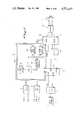
- the apparatusprovides for communication of data and control commands over a telephone line to a remote site.
- the apparatus of FIG. 1provides a data communication unit which generally includes a data terminal 1, an RS-232 interface 2 (port 1) and a modem 3 coupled by a hybrid circuit (port 2) to the ring (R) and tip (T) conductors of a telephone line 4.
- the RS-232 interfacerefers to a standard established by the Electronics Industries Association which defines the signal interface couplings between data terminal equipment and data communications equipment employing serial binary data interchange.
- the term "data terminal”refers to any external device having an RS-232 interface for providing or receiving digital data.
- the data terminalmay be a computer, including any of the so-called "personal computers.”
- the data terminalmay be a printer or an information display system.
- a parallel interfacemay be used and such would be fully functionally eqivalent to the serial interface in the context of the present invention.
- the general function of the modem 3is, of course, to send and receive digital data.
- the modemaccepts digital data from a data terminal and places a transmit data signal on a telephone line for communication to a remote modem coupled to a data terminal.
- the transmit data signalis an analog signal obtained through modulation of a carrier by a digital input.
- the transmit data signalwill contain data from the data terminal which has been encoded into the appropriate signal structure according to the applicable Bell Telephone or CCITT standards. It is to be understood that the modem also places signals on the telephone line that allow the answering modem to link with the originating modem.
- DTRdata terminal ready
- RTSrequest to send
- DSRdata set ready
- CXRclear to send
- CXRCarrier
- a control circuit in the form of a processoris provided to direct the overall operation of the modem and execute a sequence of instructions to control the various elements of the modem.
- the processorincludes a central processing unit (CPU) 12 and a program read only memory (ROM) 14.
- the program ROM 14contains instructions for directing the various operations necessary to effect the overall operation of the modem.
- the CPUobtains instructions from the ROM 14 and interacts with the various modem elements over a data bus 16 and an address bus 18.
- CPU 12is coupled to the data bus by a data bus buffer 20.
- the CPUis coupled to the address bus by an address bus buffer 22.
- An input latch 24is also coupled to the data bus and receives inputs to be obtained by the CPU during the course of its operation.
- An output latch 26couples to the data bus and permits the CPU to place output information to elements requiring command code inputs. Also, among the outputs from the CPU handled by the output latch 26 are the DSR, CXR and CTS outputs to the data terminal.
- control circuit functions of data control and modem controlmay be assumed by the data terminal.
- the CPU in the data terminalmay in accordance with appropriate software instructions provide some or all of the functions of data and modem control.
- a separate circuit, peripheral to both the data terminal and the modemmay be interconnected to provide the control circuit functions.
- data for communicationmay be otherwise provided.
- communicationmay be to a remote modem coupled to a remote data terminal serving as a remote data source and receiver
- other data receiversare contemplated.
- the remote modemmay be interfaced to a remote data receiver in the form of an information display system such as a printer or character generator for a display device.
- a remote data receivermay include data transmission capability, for communication back to the local site.
- the modem 3 in FIG. 1further includes a transmit data buffer 28 receiving digital data from the data terminal for communication.
- the transmit data buffermay be physically located on either side of interface 2. Also, the buffer can be within the data terminal or in an interconnected peripheral.
- the datais routed through serial I/O device 40 onto the data bus 16. Digital data from the transmit buffer is provided via serial I/O device 40 to a transmitter 30.
- the transmitteris selectively operable to transmit in either a higher-speed, half-duplex mode or in a lower-speed, full-duplex mode. Selection of the particular mode of operation is under the direction of the processor.
- the transmitter outputis coupled to the ring and tip conductors of the telephone line by a hybrid circuit 32. Coupled to the hybrid circuit 32 is a receiver 36.
- the receiveris capable of receiving at various data rates and in various modes. Selection of one of the receiver outputs is made by a multiplexer 38.
- the serial interface circuit 40under the direction of the processor provides received data for passage through the RS-232 interface to the
- the transmit bufferholds data from the data terminal.
- the transmitterreceives data from the transmit data buffer and places a transmit data signal on the telephone line.
- the transmitteris selectively operable in either a lower-speed, full-duplex mode or a higher-speed, half-duplex mode in response to a mode control command from the processor.
- the processormonitors the amount of data being held in the transmit data buffer and produces the mode control command to the transmitter to establish the mode of transmitter operation based upon the amount of data in the transmit data buffer.
- the processorselects the lower-speed, full-duplex mode of transmission.
- the lower-speed modecannot prevent the buffer from rapidly filling.
- the processordetermines that a predetermined number of characters is reached in the transmit data buffer, it directs the transmitter to enter the higher-speed mode of operation.
- the processordetermines and can direct the transmitter to enter the lower-speed mode.
- the initial exchange of link parameters and other required control frame exchangesproceeds with the transmitter being directed to operate in the lower-speed, full-duplex mode.
- the processordirects the transmitter to operate in the higher-speed, half-duplex mode.
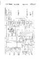
- FIG. 2there is presented a functional diagram of the telephone line interface and power supply circuits.
- the power supply(not shown) is conventional and provides voltage levels of +12, +5, -12, and ground.
- the power supply outputis applied to power supply filtering circuits to obtain the voltages for operating the various circuit elements.
- the hybrid circuit 32is shown to receive the analog signal to be placed on the telephone line. This signal is provided over conductor 33.
- the analog signalis applied to an isolation line transformer 52 having protective diodes 53 and filter capacitor 54 connected across its terminals.
- the transformeris coupled to the tip and ring conductors of the telephone line connector by a hook control relay 56. Also connected to the tip and ring conductors is ring detect circuit 58.
- Signal path 60includes a gain stage 63 and equalizer circuit 64.
- Signal path 61includes gain stage 65.
- Signal path 62includes bandpass filter 66 and envelope detector 67. The outputs of the signal paths are variously applied to the circuitry shown in FIGS. 3 and 4.
- FIGS. 3 and 4there is presented a more detailed functional diagram of the modem which is generally diagrammed in FIG. 1.
- the embodiment being describedutilizes a microprocessor as the control circuit. Accordingly, there is provided a data bus 70, an address bus 72, and the control bus 74.
- the CPU 80is coupled to the data bus by data bus buffer 82 and coupled to the address bus by address buffer 84. Coupled to the data bus are input latches 86, 88, and 90.
- Latch 86accepts and holds signals from the data terminal interface.
- Latch 88holds various internal modem signals.
- Latch 90holds various inputs from the front panel switches.
- the latch enable signalsare provided from decoding circuits 92 which is coupled to the control bus 74 and address bus 72.
- the program for execution by the processoris contained in program ROM 94.
- This ROMis addressed by addresses output from the CPU over the address bus 72, and the ROM contents are provided to the CPU over data bus 70.
- the selection of the ROMis also under the direction of the CPU through decoding circuits 92.
- Digital data from a data terminal for communicationis placed in the transmit data buffer which includes random access memories 96 and 98. Additional random access memory storage is provided by random access memory 100.
- This memoryis a nonvolatile memory that stores information such as telephone numbers and other information which is historical.
- a battery circuit 102maintains the contents of RAM 100 during the time power is off. Also, during the time of resetting the processor, battery circuits 102 disables RAM 100.
- a combined transmitter/receiver device 104This device is suitably an R96FAX system available from the Semiconductor Products Division of Rockwell International Corporation.
- Device 104is coupled to the data and address busses in order to receive directions as to the configuration for the operation desired.
- Serial digital data for serving as the modulating signalis provided to device 104 on the TXD line 105.
- the serial digital datais routed through a multiplexer 106.
- the TXD signalis obtained from serial input/output device 110 through switch 112.
- Device 110is coupled to the data bus and receives frames of data from the data buffer random access memories 96 and 98 under the direction of the CPU.
- Digital data from the data terminalis provided through the RS-232 interface and applied serially to device 110 for conversion to parallel form.
- the CPUdirects the parallel-form data from device 110 to data buffer random access memories 96 and 98.
- the CPUmonitors the data frames being placed in the data buffer and keeps a running tabulation of the amount of data being placed in the data buffer.
- the TXD serial data stream from the RS-232 interfaceis passed around device 110 over line 114 and applied through switch 112 to multiplexer 106. It is only in the asynchronous mode of operation that the CPU directs data to be communicated through the serial input/output device 110.
- the transmitterfurther includes a lower-speed, full-duplex transmit and receive device 116.
- the serial data stream TXDis applied to the lower-speed transmitter/receiver device 116 from multiplexer 106 over signal path 118.
- Control of the lower-speed device 116is provided by the CPU. Configuration and control instructions are placed in output latch 120 and provided to device 116.
- the R96 FAX system implementing device 104is a slow turnaround device.
- the use of the full-duplex device 116provides fast carrier acquisition and link management.
- the fast carrier acquisition facility in combination with the high data throughput facilityprovides the desired high-speed data transmission over dial-up telephone lines and a full-duplex appearance at the data terminal interface.
- the modemincludes a dual tone multifrequency (DTMF) generator 122 which provides tones for dialing.
- Device 122is controlled by the CPU with control commands placed in output latch 124.
- the analog transmit signal from the lower-speed transmitter 116is applied to an amplifier 126.
- the output from tone generator 122is also provided as an input to amplifier 126.
- the output of amplifier 126 and the analog transmit signal from higher-speed transmitter 104are applied to a buffer amplifier 128.
- the output of amplifier 128is the modem transmit signal applied over line 33 to hybrid circuit 32 in FIG. 2.
- driver 130providing signals to the RS-232 interface. Certain of the signals provided to the drivers are obtained through output latch 132 which is loaded through the data bus.
- Another output latch 134 connected to the data busprovides controls for the front panel light-emitting diode displays 136.
- the receive signal paths 60 and 61provide the transmit signal from a remote modem to the lower-speed and higher-speed receiver portions, respectively.
- the signal RXA shown in FIG. 4is being applied to device 104 which yields the receive signal on line 140.
- This signalis applied in FIG. 3 to multiplexer 142.
- the signal on line 40is applied to the serial input/output device 110.
- the CPUmay obtain received data from device 110 or direct passage of the serial data onto switch 144.
- the output from switch 144is applied through driver 146 to the RS-232 interface as the receive signal RXD.
- the receive signal from signal path 60 in FIG. 2is applied to the lower-speed device 116.
- the receive signal from device 116is provided over line 148 to multiplexer 150 in FIG. 3.
- the output of multiplexer 150is applied to the input of the serial input/output device 110.
- the CPUacquires the receive signal data to descramble it and provide it back through device 110 to line 143 to become the RXD output to the data terminal interface.
- a counter timing circuit 160is controlled by the CPU.
- Device 160includes timers which can be turned on or off by the CPU.
- Device 160generates the various baud rate timing signals for the serial input/output communication device 110 from the T0 output over line 161.
- Another timer in device 160provides a signal from output T1 over line 162 to multiplexer 164. When line 162 is selected by the multiplexer to be applied to device 110, the signal is provided to device 110.
- FIGS. 5-13there is presented a detailed implementation of the modem diagrammed in FIGS. 1-4. This implementation corresponds to the Racal-Vadic Model 9600 VP modem product.
- the 9600 VPis a triple speed switched network modem that a user can operate at 9600 bps, 1200 bps, or 300 bps asynchronously, as well as 9600 bps, 7200 bps, 4800 bps, or 1200 bps synchronously.
- the 9600 VPprovides full-duplex terminal operation in all asynchronous modes and 1200 bps synchronous. Operating synchronously, the 9600 VP provides half-duplex terminal operation at 9600 bps, 7200 bps, or 4800 bps.
- Modem operationincludes a link protocol which involves dynamically switching between a full-duplex, lower-speed mode for data acknowledgments and interactive transfers, and a half-duplex, higher-speed mode for data transfer.
- the modemcan keep its transmit data buffer from filling using the lower-speed mode, it will not go to high speed.
- the modemcannot keep the buffer from filling and as the predetermined number of characters is reached, the higher-speed mode is entered, emptying the buffer at 9600 bps, while the far end transmitter buffers its data. The modem then drops back to the lower-speed mode for acknowledgement. This operation repeats based on data transmission demand. Switching between modes is transparent to users in all cases where the transmitted data is distributed unevenly or asymetrically (i.e., more data from one end than from the other end). Asymetrical distribution of data is typical of most applications, except for some mainframe file transfer applications and multiplexer applications.
- CCITT V.29 and V.27 modulations(9600, 7200, 4800 and 2400 bps) are used for the higher-speed, half-duplex mode, and Bell 212A is used for the full-duplex, lower-speed mode.
- the modemalso conforms to Bell 212A and 103 standards.
- the modemincludes, among other features, full-duplex emulation, a superset MNP error correction protocol, data compression/decompression, automatic speed detection, as well as fall-back and fall-forward operation from 9600 asynchronous mode, speed conversion, auto dialer command sets, front panel operations, and auto answer/originate. Automatic origination is accomplished by an integrated automatic dialer operated from the data terminal keyboard, the modem front panel, or communication software for unattended operations.
- the modemis packaged in a VIP II standalone case having membrane switches, an LED display, and jacks for detachable interconnection of programmable line connections, RS-232 interface, and power cables.
- connection of the modem to the Data Terminal Equipment (DTE)is through an EIA RS-232 interface.
- the interface connections according to connector pin numberare as follows:
- the modemoperates in five basic states: Idle, Data, Dialing, Interactive, and Test. These states can be entered by various commands from the Data Terminal Equipment (DTE), the modem front-panel keyboard, or through automatic operation.
- DTEData Terminal Equipment
- the Idle Stateis the power-up state of the modem. Pressing the /RESET/ key at any time will return the modem to this state.
- the modemWhen in the Idle State, the modem is ON HOOK, and will automatically answer an incoming telephone call. It is also prepared to respond to front panel or DTE comments. A phone plugged into the rear panel "TelSet" jack is connected to the phone line.
- the Idle stateis entered from the Data state on loss of DTR or receipt of the on line disconnect code, loss of received carrier in 212 or 103 mode, or a specified number of consecutive unanswered link requests in 9600 mode. It is also entered from the Interactive State upon expiration of the activity timer or when the Idle Command is issued.
- the Data Stateis the on-line communications state of the modem. This state is entered from the Idle state through the auto answer function in response to a ringing signal on the phone line or when the /DATA/ or /ANS/ keys are pressed. The Data state is entered from the Dialing state at the completion of any log-on sequences.
- the modemis equipped to automatically detect that a connection has been established with another 9600 VP, a 212A or 103. The modem will automatically identify a remote 9600 VP.
- the handshake protocolis depicted in the line drawings in FIG. 14. There are four types of modem handshakes and one error control handshake.
- the modemIn asynchronous Originate mode, the modem attempts its proprietary handshake designed to identify another 9600 VP. If this handshake fails, the modem automatically attempts a 212A handshake. If this fails, the modem attempts a 103 handshake, if this fails, the modem reports "failed call" and disconnects the line.
- the auto answer modethe 9600 VP attempts its own 9600 VP handshake first. If this fails, a 212A handshake is attempted. If this fails, the modem attempts a 103 handshake, and if this fails, the modem disconnects the line. No call progress messages occur on the auto answer side.
- the modemattempts a proprietary handshake at 9600, 7200 or 4800 bps as indicated by the speed key LED.
- the 1200 bps synchronous handshakeis the Bell 212A standard.
- An error control protocolis entered by completing the proprietary 9600 VP asynchronous handshake (212A handshake with scrambled SPACE) with another 9600 VP.
- the Error Control Modeprovides for synchronous data packets operation and enables selective ARQ, dynamic fallback/fallforward, and data compression with an outstanding packet window of 12.
- commandsare issued to the modem to control its operation or to configure its operating characteristics.
- the modemstores the last interactive mode, and uses this memory in order to respond appropriately for auto answering. Commands and response are transmitted over the RS232 leads to the modem.
- This modeThere are two versions of this mode available. (1) The Vadic interactive mode and (2) the "AT" command mode.
- the Vadic interactive modeis entered from the Idle state when the characters (!E)(CR) are received from the DTE. If a call is initiated from the interactive mode, and you receive loss of received carrier, or DTR or receive the On-Line Disconnect code, you leave Interactive Mode and enter Idle Mode. Upon "failed call", you remain in Interactive Mode. You remain in the Vadic Interactive Mode until the two-minute inactivity timeout.
- the Vadic optionstake precedence over the "AT” options, and continue to do so in all other modem states (i.e., Idle, Data, Test, etc.)
- the "AT” command modeis entered from the Idle state when the characters "AT" are received from the DTE.
- the "AT” modetake precedence over the Vadic mode, and continues to do so in both command and data states.
- Either the Vadic or the "AT" modescan be selected any time the modem is in the Idle or Command State by sending the appropriate commands to it. Once the "AT" command set is entered, the modem must return to the Command mode before the Vadic Interactive Mode can be entered.
- commandsare issued by pressing the keys on the front panel.
- the responsesare displayed on the DTE.
- the modemexecutes the dialing instruction stored in its dial-instruction register.
- the dial commandis placed there by the Dial and Dial Stored Number terminal commands as well as by depressing the /REDIAL/ or the /DIAL/ Memory Location front panel keys.
- the Dialing stateis entered from the Idle state by pressing the front panel /DIAL/ (Stored Number Memory Location) and /ENTER/ keys or /REDIAL/ keys.
- the dialing stateis also entered from the Vadic Interactive Mode through the Dial, Dial Stored Number, and Redial Interactive commands.
- the Vadic dialer sequencemay be aborted through the front panel /RESET/ command or by entering any character from the DTE.
- This statemay also be entered from the AT Interactive mode through the ATD -- (CR) command.
- the "AT" dialer commandmay be aborted by sending any character to the modem from the DTE before the call is completed. If dialing is aborted from the DTE or the call fails, the modem returns to the state that invoked the dialer.
- Vadic call progress messagesinclude: Dialing, Busy!, disconnect, Ringing, No Dial Tone, Answer Tone, Error Control, Selected Speed Unavailable, On-Line, On-Line 300, On Line 1200 and On Line 9600.
- the modemIn making a call, after dialing the last digit of the phone number portion of the dialing instruction, the modem will wait up to 60 seconds for valid carrier. If valid carrier is not received within this time, a "FAILED CALL" message will be displayed and the modem will return to the state that invoked dialing.
- the Test stateencompasses the many test functions provided to enable an operator to locate a failure in the data communications link via Analog or Digital Loopbacks.
- the Test statemay be entered from Idle state and Data state though the front panel keys and from Vadic mode or from the Terminal Interactive state through the test commands in Vadic mode only.
- the front panel of the modemconsists of ten LEDs and a 12-position keypad with eight additional LEDs.
- the ON/OFF condition of the LEDsrefers to the operational state of its respective switch.
- the keypadhas most keys serving dual functions.
- the /DIAL/ keyshifts all keys to their numeric functions. The keys are restored to nonnumeric function by the /ENTER/ key.
- the /DIAL/ keycan only be followed by a one or two digit memory location number of stored phone numbers which is followed by the /ENTER/ key.
- the /DIAL/ and /REDIAL/ keyscause call progress messages to be put out to the DTE at the speed and parity of the last auto baud. The call progress messages are not sent to the DTE when using the /REDIAL/ or /DIAL/ keys with the synchronous LED ON, nor are they sent when manually originating or answering a call.
- the ANS LEDindicates the status of the two answer modes, auto answer and manual answer.
- Auto Answer /ANS/ key LED ONthe modem will automatically answer the phone line assuming DTR is present or forced.
- /ANS/ key LED OFFmeans the modem will not answer the phone.
- the modem that will be the answer sidemust have the /ANS/ key LED ON; the originate side modem should have its /ANS/ key LED OFF.
- the modemwill display the following EIA interface parameters with LED indicators:
- the functions of the front panel key switchesare:
- FIGS. 1-4In a view of the description of FIGS. 1-4, a detailed description of the schematic diagrams of FIGS. 5-9 is unnecessary. However, to indicate the correspondence between FIGS. 1-4 and 5-9, the following description is provided.
- FIG. 6corresponds to the diagram of FIG. 2, including the power supply, telephone line interface/hybrid, and received signal paths.
- FIGS. 6-9correspond to the diagrams of FIGS. 3 and 4 as follows:
- FIG. 10there is presented a diagram illustrating the connect sequence for the modem of FIGS. 1-4 and 5-9.
- the diagramillustrates the transmitted and received signals for both an originate modem and an answer modem.
- the remote central officesends a ring signal to the answer modem which is detected on the ring indicator RI line.
- the answer modemgoes off-hook and transmits an answer tone of 2225 Hz. This tone is received by the originate modem and after 455 milliseconds, the originate modem begins sending a carrier modified by logic 0 data, referred to as scrambled zeros for 100 milliseconds followed by scrambled ones.
- the answer modemAfter approximately 50 to 100 milliseconds of scrambled zeros being received, the answer modem identifies that the originating modem is compatible and transmits scrambled zeros back to the originate modem. The originate modem then identifies that the answer modem is compatible.
- the modemsthen exchange link parameters for error control.
- the originate modemfirst sends approximately 23 bytes of link parameter information.
- the answer modemreceives the link parameters and if any parameters need to be changed, it sends update link parameters to the originate modem. After the update link parameters are exchanged, the CXR and CTS lines are turned on at both modems.
- the modemsWhen enough data accumulates in the transmit data buffer at either end to go high speed, the modems exchange control frames. Both modems then go into a squelch for a period of time, and the transmitter of the corresponding modem begins sending data at 9600 bps. At the end of data transmission, the modems squelch and 1200 bps, full-duplex transmission is resumed and acknowledgments sent for frames received. The speed is maintained until it is time for either modem to transmit data to the other modem at higher speed. At that time, both modems squelch, and thereafter the operation continues as described above. Data transmission proceeds as required by the data transmission demands of the data terminals for the modems.
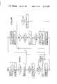
- FIG. 11there is a flowchart of the data transmission routine followed by the modem operating as an originate modem.
- the modemperforms the originate/answer connect sequence by calling and establishing a link with the answer modem in a lower-speed, full-duplex mode.
- the modemthen enables the sending and receiving of data to the data terminal equipment. If the link parameters do not agree, the modem disconnects.
- the originate modemasks the remote modem to go lower-speed, full-duplex and to send an acknowledgement.
- the modemsestablish the lower-speed, full-duplex link.
- the modemchecks for acknowledgment from the remote modem. If the acknowledgement does not come within a prescribed time out period, the modem initiates a recovery to establish the lower-speed link. If the acknowledgment is received, the modem determines whether the remote modem has requested higher-speed operation. If so, the originate modem acknowledges the request for higher-speed and establishes the half-duplex link and sets up in a receive mode. There continues to be monitoring for a request to go lower-speed.
- the modemWhen the request is received, the modem establishes the lower-speed, full-duplex link and sends an acknowledgement that all data frames have been received. The received data frames are decompressed and sent to the data terminal. The originate modem then returns to check for any data from the data terminal. The diagrammed sequence continues until completion of the required data communication task.
- FIG. 12flowcharts an operational sequence of the modem involving data communication that automatically changes between speeds of transmission based upon data transmission demand during a communication and upon the quality of the data transmissions.
- the modembegins transmitting, it checks for data from the data terminal. The data for transmission is compressed and stored in the transmit data buffer. Next, there is evaluation of whether any data is waiting for retransmission. If so and there is enough to go higher-speed, the modem sends control frame information to the remote modem to go higher-speed. The higher-speed, half-duplex link is set up and transmission of data begins. At the conclusion of data transmission, a control frame is sent requesting the remote modem to go into the lower-speed mode. The modem then awaits reception of an acknowledgement. If the acknowledgement does not come within a prescribed time out period, the modem initiates recovery by establishing the link and reentering the transmit sequence. If the request to go lower-speed is acknowledged, the routine goes back to the beginning of the transmit sequence.
- a predetermined number of data frameshave been transmitted at higher-speed (e.g. 25 frames). If so, there is a check to determine whether the transmitted data frames included any retransmissions. If there was retransmission of any data frame for a predetermined number of times (e.g. 8 times), there is a calculation of the retransmit frame ratio. Based upon the calculated ratio, a determination is made whether the quality of the data transmission indicates qualification for a fallback in speed. If there had been retransmission of any data frame at least the predetermined number of times, and if the modem is linked in the lowest fallback speed, then the modem disconnects. If the link is not in the lowest fallback speed, the modem sets up the link for one step lower in speed and reenters the transmit sequence.
- the routinemakes an evaluation for qualification to fallforward to a higher speed. If the qualification is not met, the transmit sequence is reentered at the same speed. But if the data transmission quality qualifies for a fallforward in speed, and the link is not already in the highest speed, the modem sets up the link for a one step higher speed of transmission.
- the routine in FIG. 12illustrates the ability of the modem to adapt its speed to the quality of the telephone line.
- the modemcan either fallback to a lower speed or fallforward to a higher speed.
- the processor of the modemconstantly monitors the number of errors in data transmission as reflected by the number of retransmitted data frames. If the number of retransmissions is high, indicating too many errors are encountered and line quality is poor, the modem drops down to the next lower speed until an acceptable reduction in errors in transmission is achieved. If the line quality improves and the number of errors is reduced, the modem will automatically fallforward to the next higher speed.
- FIG. 13provides a listing of the program ROM contents for the modem implementation of FIGS. 5-9.
- This programincludes the routines diagrammed in FIGS. 10-12 as well as other operations for the modem described above in FIGS. 5-9.
Landscapes
- Engineering & Computer Science (AREA)
- Signal Processing (AREA)
- Computer Networks & Wireless Communication (AREA)
- Quality & Reliability (AREA)
- Communication Control (AREA)
- Telephonic Communication Services (AREA)
- Detection And Prevention Of Errors In Transmission (AREA)
Abstract
Description
______________________________________ PIN SIGNAL ______________________________________ 1 Chassis (Protective) Ground (FG): This is protective ground, tied to the AC power ground of the terminal equipment and is isolated from the signal ground (Pin 7; SG) unless optionally strapped. 2 Transmitted Data (TXD): (To Modem) Signals on this line are generated by the Data Terminal Equipment and transferred to the modem for transmission to the Remote Data Terminal equipment. The modem will transmit accept data from this line when an ON condition is present on the CTS line. 3 Received Data (RXD): (From Modem) Signals on this line are generated by the modem receiver in response to signals transmitted by the remote modem except when the modem is in a test mode. This line is clamped to "MARK" whenever the CXR circuit is OFF. 4 Request to Send (RTS): (To Modem) The signal on this line is normally generated by the DTE for use in half-duplex modems. In synchronous 9600, 7200, 4800 bps modes, an ON condition of the circuit is an indication to the local modem that the DTE wishes to send data. After the RTS circuit is turned ON, the DTE waits for an ON condition of the CTS circuit before starting transmission. In 212/103/9600 full-duplex operation, if RTS circuit is ON, CTS will go ON. 5 Clear to Send (CTS): (From Modem) An ON condition of the CTS line indicates to the terminal equipment that the modem will transmit any data which is present on the TXD line. CTS is turned ON in response to an ON condition of the RTS line from the DTE. 6 Data Set Ready (DSR): (From Modem) In synchronous modes, this signal indicates the line status of the modem. The ON condition of this line indicates that the modem is connected to the telephone line (OFF-HOOK) and is capable of transmitting and receiving data signals. Both DSR and CTS are required to be ON to transmit data. 7 Signal Ground (SG): Common ground reference point for all interface circuits. 8 Carrier Detect (CXR): (From Modem) Informs the DTE that the modem is receiving a data signal suitable for demodulation. 9 Testing Voltage (+V): (V = 12.5 ± 2.5 V) 10 Testing Voltage (-V): (V = 12.5 ± 2.5 V) These signals provide test points to verify the presence of power in the modem. 11No Connection 12No Connection 13No Connection 14No Connection 15 Serial Transmit Clock (SCT): (From Modem) This digital interface line is associated with the high or medium speed synchronous format when the transmit clock is set for internal timing. The signal on the SCT is a square wave and is used to provide the DTE with a signal element of the transmitted data (TXD) circuit. This signal is turned OFF when in asynchronous mode and turned ON when in synchronous mode. The first signal element of the transmitted data signal should be presented by the DTE on a positive (OFF to ON) transition of SCT which occurs after the CTS circuit has turned ON. The transmitted data is sampled by the modem on negative transi- tions of SCT. 16No Connection 17 Serial Receiver Clock (SCR): (From Modem) This interface circuit is associated with the synchronous format in the high or medium speed mode. The squarewave signal on this circuit is used to provide the DTE with receiver timing information for the RXD circuit. This signal is turned OFF when in Async mode and turned ON when in Sync mode. The ON to OFF (negative-going) transition on circuit SCR indicates the center of each signal element on the RXD circuit. 18 NoConnection 19No Connection 20 Data Terminal Ready (DTR): (To Modem) Control signal used to prepare the modem for connection to the communications channel and maintain the connection once established. In automatic answering applications, the modem will connect to the line upon receipt of the trailing edge of the ringing signal if DTR is ON. DTR may be forced on internally regardless of interface voltage by programmable option. DTR must be turned ON for the modem to automatically originate or answer a call. 21 NoConnection 22 Ring Indicator (RI): (From Modem) The ON condition of this line indicates that a ringing signal is being received by the modem. The ON condition is approximately coincident with the ON segment of the ringing cycle. When the telephone line is OFF-HOOK, or when ringing stops, the RI line will turn OFF. 23No Connection 24 External Serial Transmit Clock (SCTE) (To Modem) Synchronous operation requires signals on this line to provide the modem transmitter with signal element timing information from the terminal when the external transmitter timing strap option is selected. The ON to OFF transi- tion of this circuit should nominally indicate the center of each signal element on the TXD circuit. 25 No Connection ______________________________________
______________________________________ EC ERROR CONTROL LED flashes from ON to OFF. The Error Control LED is ON when the modem is hooked up in error control mode. This LED flashes OFF with each retransmission of data. During diag- nostics, the EC LED is normally OFF and flashes on with errors. TXD TRANSMIT DATA (flashes when transmitting "DATA"). RXD RECEIVED DATA (flashes when receiving "DATA"). HS HIGH SPEED asynchronous: OFF = 103, 1200; ON = 9600, 7200, 4800 or 2400 bps; synchronous: OFF = 1200, ON = 9600, 7200, 4800 bps. CTS CLEAR TO SEND (ON = CTS raised). DSR DATA SET READY (ON - Modem Off-Hook, computer system interface or test modes; OFF= Idle or interactive). DTR DATA TERMINAL READY (ON = Automatic Operation Enabled). RI RING INDICATOR follows the detected Ring Envelope. CXR CARRIER DETECT (ON = Carrier Received or com- puter system interface). PWR POWER (ON = Power ON). ______________________________________
______________________________________ ##STR1## This key places the modem into InteractiveMode and redials the last number dialedautomatically. The call progress messages are put to the DTE at the last auto baud speed and parity. This key can be used to dial when in Sync mode. However, call progress messages are not set to the DTE. When in numeric mode, this key enters thedigit 1. ##STR2## This command may be issued when the modemis in the Idle State. This key can beused to dial a memory location and hook up synchronously if the SYNC LED is ON. There are no call progress messages sent when the Sync LED is ON. The front panel keys are shifted to numeric and the memory address of a dialing ##STR3## Sync LED is OFF, the address prompt and address number as well as the telephone number are displayed on the DTE and dialing beings. The call progress messages: "Dial Tone", "Dialing", "Ringing", "Busy", "On Line"↑, "OnLine 300", "OnLine 1200", "OnLine 9600", "Ans Tone", "Speed Selected Unavailable", "Error Control", "Disconnected", and "Failed Call" are displayed as appropriate. When in numeric mode, this key enters thedigit 2. ##STR4## When in the Idle Mode, pressing this keyputs the modem into the Analog LoopbackTest Mode, busies out the telephone line and lights the ALB LED indicator. When in numeric mode, this key enters thedigit 3. ##STR5## When the data mode, pressing this key putsthe modem into the digital loopback testmode and lights the DLB LED. In addition the DLB LED will go ON when an RTRT is received. The Digital Loopback Test has two modes. They are Local Digital Loopback, entered when the speed key indicates 300 bps (SPEED key LED OFF) and Remote Digital Loopback, which is conducted at 1200 (SPEED key LED red ON). When in numeric mode, this key enters thedigit 4. ##STR6## When in the Data or Test Modes, pressingthis key enables the self-test circuitryand lights the SELF TEST indicator. This circuitry generates and detects a testing pattern and if an error occurs, the EC LED indicator flashes. After self-test is enabled, pressing this key again ends the self-test, while the modem remains in its current mode (Data, ALB, or RDLB). When in Numeric Mode, this key enters thedigit 5. ##STR7## From any mode, this key activates a hardwarereset which causes the modem to godirectly into the Idle Mode. If the modem was last in Vadic mode, the modem could auto answer the next call. If last mode was "AT", then "AT" messages are output. ##STR8## This key puts the modem in either Data orVoice Mode. The modem powers up in VoiceMode. When the LED is ON, this indicates the modem is attached (OFF HOOK) to the phone line. Pressing the key switches the modem to Data Mode, light- ing the data LED indicator, and the DSR LED. When in numeric mode, this key enters thedigit 6. ##STR9## This key selects the speed the modem willattempt to establish a manual connectionor test. When dialing from the DTE, the last auto baud speed will be reflected by the SPEED key LED when the modem is in Idle or Interactive mode. The SPEED key reflects the data line speed when on-line. The SPEED key LED light will go off when 300 bps is selected. The LED will go red if 1200 bps is selected and will go green if the 9600 bps speed is selected. In synchronous mode, the SPEED key LED light will go OFF when 1200 bps is selected, Red when 7200/4800 is selected, and green when 9600 is selected. When in numeric mode, this key enters thedigit 7. ##STR10## ##STR11## ##STR12## the modem will manual answer. To auto answer, the DTR LED should be ON, ##STR13## the modem is ON HOOK. Upon receiving a ring indicator signal, the modem automatically gives OFF-HOOK and sends answer tone. When in numeric mode, this key enters thedigit 8. ##STR14## From Idle, Interactive, Dialing and test States, this key causes the current data format, modulation, speed and communications mode to toggle between SYNC and Async. The SYNC LED lights when in SYNC mode. This key automatically updatesOption 14. Changes inOption 14 automatically update this LED after RESET has been depressed. When in numeric mode, this key enters thedigit 9. ##STR15## When in numeric mode, this key enters thedigit 0. ##STR16## When in the front panel interactive mode,this key indicates the end of a memoryaddress key. ______________________________________
______________________________________ FIG. 6 FIGS. 3-4M33 CPU 80 M18, M25, M34 I/86, 88, 90 M23, M41, P Latch M42 Buffer 82, 84 M26 EPROM 94 M49,M22 Address Decode 92M32 MUX 142 FIG. 7 FIGS. 3-4 M19,M11 RAM 96, 98M35 RAM 100 M53 Serial I/O 110M48 Timer 160M54 MUX 164 FIG. 8 FIGS. 3-4 M10, M13 XMTR/RECR 116 M45 DTMF Gen. 122 M31, M39 O/120, 124 P Latch 126, 128 FIG. 9 FIGS. 3-4 M5 O/ M12 Amp P Latch 134 M8, M52 O/P Latch 132 M29,M37 EIA Drivers 130 ______________________________________
______________________________________ Part Ref. Description Designation ______________________________________ IC,4013B,CMOS DUAL D-FF M38 M44 IC,4020B,CHOS 14 STG BIN CNTR M9 M28 IC,74LSO4N,TTL HEX INVERTER M15 IC,74LS138N,TTL DECODER/DEMUX M22 M49 IC,74LS02N,TTL GUAD 2-INP NOR M46 IC,74LS08N,TTL QUAD 2-INP AND M36 M51 IC,5089,DTMF TONE GENERATOR M45 IC,6116P,CMOS 2K × 8 RAM M35 IC,74LS21N,TTL DUAL 4-INP AND M55 IC,74HCO4N,CMOS HEX INVERTER M21 M47 IC,74HC244N,CMOS OCTAL BUFFER M18 M23 M25 M34 M41 IC, 74HC245 BUFFER M42 IC,74HC74N,CMOS DUAL D-FF M40 IC,74HC373N,CMOS OCTAL D LATCH M5 IC,74HC273P,CMOS OCTAL D-FF M8 M31 M39 M52 IC,TC5564P-1,CMOS RAM 8K × 0 M11 M19 IC,74HC153 DUAL 4-INPUT MULTIPLEXER M32 M54 IC,Z80B SERIAL I/O M53 IC,CTC,Z80B COUNTER TIMER CKT M48 IC,Z80B,CPU M33 IC,74LS38N,TTL 2-INP NAND BFR M14 IC,74LS155,TTL DECODER/DEMUX M16 M17 IC,4558,DUAL AMPL NPN & PNP IN M2 M4 M12 M29 M37 IC,1489P,QUAD LINE RECVR M30 IC,4053B,CMOS 2 CHAN MUX/DEMUX M7 M24 M27 IC,393N,VOLTAGE COMPARATOR M6 IC, DUAL JFET OP AMP, 353N M43 M50 IC,SSI262,212A CHIP M13 IC,SSI261,212A CHIP M10 DIODE, SILICON, GP 1N4148 CR3 CR8 CR9 CR13 CR15 CR39 DIODE, SILICON, SCHOTTKY, 1N6263 CR11 CR12 LED, HIGH EFFICIENCY, RED CR19 CR35 LED, BI-COLOR,RED/GREEN CR36 DIODE, GER, IN270 CR14 CR37 DIODE, ZENER 5.6V 5%, 1N752A CR10 DIODE, ZENER, 5.1MW, +-5% CR18 DIODE, SI ZENER, 27V, 1N5254 CR1 CR2 DIODE, SILICON ZENER, 6.2V, 1N4735 CR6- CR7 DIODE, SILICON ZENER, 6.8V, 1W, 5% CR17 RECT, SILICON, 1N4005 CR16 XSTR, NPN, 2N3904 Q2- Q3 XSTR,ARRAY, QUAD N-P-N SILICON M20 PXSTR, OPTO-ISOLATOR, 4N35 M1 RELAY, ELECTROMECHANICAL K1 FERRIT BEAD,A.138,B2.75,C.35 FB1 XTAL, QTZ, 3.686400 HNZ Y4 XTAL, QTZ, 5.5296 MHZ Y2 RES, CARD, 1.0K, 1/40, 5% Y3 R40 R46 R59- R60 R62- R63 R68 R84- R85 R94- R98 R100 R107 R120 R126- R128 R132 RES, CARB, 100K, 1/4W, 5% R6 R9 R42 R74 RES, CARB, 1.0 M, 1/4W, 5% R56 R64 R91 RES, CARB, 1.2K, 1/4W, 5% R44 RES, CARB, 200K, 1/4W, 5% R111 RES, CARB, 2.0M, 1/4W, 5% R88 RES, CARB, 20.M, 1/4W, 5% R8 RES, CARB, 220., 1/4 W, 5% R57 R73 R92 R99 RES, CARB. 2.4K, 1/4W, 5% R23 RES, CARB, 2.7K, 1/4W, 5% R31 R80 RES, CARB, 27K, 1/4W, 5% R7 R35 R66 R72 R78 R79 R90 R103 R106 R121 R129 R130 RES, CARB, 3.0K, 1/4W, 5% R45 R58 RES, CARB, 300K, 1/4W, 5% R110 R112 RES, CARB, 2.0K, 1/4W, 5% R32 R34 RES, CARB, 360, 1/4W, 5% R89 RES, CARB, 470, 1/4W, 5% R86 R87 RES, CARB, 4.7K, 1/4W, 5% R33 R65 R69 R71 R93 R101 R102 R131 R108 RES, CARB, 560., 1/4W 5% R41 RES, CARB, 680., 1/4W, 5% R30 RES, CARB, 2.0K, 1/2W, 5% R38 R39 RES, CARB, 5.6K, 1/2W, 5% R3 RES, FILM, 383.0, 1/8W, 1%, TC-K R17 RES, FILM, 392.0, 1/8W, 1%, TC-K R18 RES, FILM, 976.0, 1/8W, 1%, TC-K R19 RES, FILM, 1.21K, 1/8W, 1%, TC-K R115 RES, FILM, 1.69K, 1/8W, 1%, TC-K R122 RES, FILM, 2.00K. 1/8W, 1%. TC-K R16 RES, FILM, 3.32K, 1/8W, 1%, TC-K R28 RES, FILM, 3.65K, 1/8W, 1%, TC-K R119 RES, FILM, 5.90K, 1/8W, 1%, TC-K R11 RES, FILM, 8.66K, 1/8W, 1%, TC-K R12 R81 RES, FILM, 8.87K, 1/8W, 1%, TC-K R25 R26 RES, FILM, 9.31K, 1/8W, 1%, TC-K R118 RES, FILM, 10.0K, 1/8W, 1%, TC-K R24 R76 R77 R83 RES, FILM, 17.4K, 1/8W, 1%, TC-K R13 RES, FILM, 21.5K, 1/8W, 1%, TC-K R54 RES, FILM, 33.2K, 1/8W, 1%, TC-K R125 RES, FILM, 42.2K, 1/8W, 1%, TC-K R123 RES, FILM, 78.7K, 1/8W, 1%, TC-K R51 RES, FILM, 100.K, 1/8W, 1%, TC-K R113 R114 R116 R117 RES, FILM, 210.K, 1/8W, 1%, TC-K R124 RES, FILM, 301.K, 1/8W, 1%, TC-K R15 RES, FILM, 464.K, 1/8W, 1%, TC-K R14 RES NET, SIP, 27KX9 RN3 RN10 RES. NET, 1K, 1/3W X9 RN2 RES. NET, DIGITAL SYS REESET CKT. RN1 CAP., MYLAR .1UF, 50V, 5% C5 C25 C43 CAP, POLYEST, RDL., .22MF, 100V, 5% C6 C32 CAP, POLYEST, RDL., 033UF, 250V, 5% C9 C18 CAP, POLYEST, RDL., .01UF, UF, 250V, 5% C7 CAP, MYLAR, .47UF, 250V, 10% C1 CAP, MYLAR, .47UF, 63V, 10% C103 CAP, CER, .1UF 50V, 10% C111 C116 CAP, CER, .1UF, 50V, 20% C34 C83 C108 C109 C150 C152 C201 C240 C244 C261 C116 CAP, CER, 27PF, 63V, 5% C68 CAP, CER, 33PF, 63V, 5% C69 C90 C119 CAP, CER, 47PF, 63V, 5% C120 CAP, CER, 82PF, 63V, 5% C118 CAP, CER, .01UF, 50V, 10% C104 C105 CAP, CER, .1UF, 50V, 10% X7R C110 CAP, TANT, 3.3UF, UF, 15V, 5% C27 CAP, ELO, 100UF, 16V, 20% C30 C38 CAP, ELO, 25V, 20UF, +75%, -10% C23 C24 CAP, CER, 220PF, 100V 10% C106 CAP, CER, 390PF, 100V, 10% C61 C73 C85 CAP, CER, 330PF, 100V, 10% C117 CAP, CER, 1000PF, 100V, 10% C26 CAP, CER, NPO, 100PF, 100V, 5% C107 DIODE, ZENER, 5.1V, 1W, 5% CR38 CONN, SOCKET, 5 POS, DIN P1 CONN, HEADER, 4 PIN P2 XFMR, SWITCHED NTWK, 600-600 OHM T1 SUPPRESSOR, TRANSIENT, 6V + -10% TS1 CAP, CER, 1500PF, 100V, 10% C153 RES, CARB, 10K, 1/4W, 5% R133 RES, FILM, 82.5K, 1/8W, 1% R82 ______________________________________
Claims (9)
Priority Applications (4)
| Application Number | Priority Date | Filing Date | Title |
|---|---|---|---|
| US06/909,012US4771417A (en) | 1986-09-18 | 1986-09-18 | High speed modem |
| EP87112112AEP0260470A3 (en) | 1986-09-18 | 1987-08-20 | High speed modem |
| JP62234714AJPS6387048A (en) | 1986-09-18 | 1987-09-18 | High speed modem |
| US07/197,128US4924456A (en) | 1986-09-18 | 1988-08-29 | High speed modem |
Applications Claiming Priority (1)
| Application Number | Priority Date | Filing Date | Title |
|---|---|---|---|
| US06/909,012US4771417A (en) | 1986-09-18 | 1986-09-18 | High speed modem |
Related Child Applications (1)
| Application Number | Title | Priority Date | Filing Date |
|---|---|---|---|
| US07/197,128DivisionUS4924456A (en) | 1986-09-18 | 1988-08-29 | High speed modem |
Publications (1)
| Publication Number | Publication Date |
|---|---|
| US4771417Atrue US4771417A (en) | 1988-09-13 |
Family
ID=25426510
Family Applications (1)
| Application Number | Title | Priority Date | Filing Date |
|---|---|---|---|
| US06/909,012Expired - Fee RelatedUS4771417A (en) | 1986-09-18 | 1986-09-18 | High speed modem |
Country Status (3)
| Country | Link |
|---|---|
| US (1) | US4771417A (en) |
| EP (1) | EP0260470A3 (en) |
| JP (1) | JPS6387048A (en) |
Cited By (34)
| Publication number | Priority date | Publication date | Assignee | Title |
|---|---|---|---|---|
| US4951309A (en)* | 1988-10-14 | 1990-08-21 | Compag Computer Corporation | Power-down modem |
| US4962378A (en)* | 1987-11-09 | 1990-10-09 | Ncr Corporation | Multi-user serial bus system |
| US5008901A (en)* | 1987-10-29 | 1991-04-16 | U.S. Robotics, Inc. | Asymmetrical duplex error-controlled modem |
| US5121382A (en)* | 1989-10-11 | 1992-06-09 | Digital Equipment Corporation | Station-to-station full duplex communication in a communications network |
| US5263083A (en)* | 1990-12-10 | 1993-11-16 | Rolm Company | Method and apparatus for sharing speakerphone processor among multiple users |
| US5289459A (en)* | 1986-12-01 | 1994-02-22 | British Telecommunications Plc | Duplex data transmission |
| US5289582A (en)* | 1986-12-27 | 1994-02-22 | Canon Kabushiki Kaisha | Communication control unit |
| US5305306A (en)* | 1990-01-22 | 1994-04-19 | Digital Equipment Corporation | Station-to-station full duplex communication in a token ring local area network |
| US5343515A (en)* | 1991-09-13 | 1994-08-30 | Treffkorn Remco V | High speed modem |
| US5377184A (en)* | 1992-03-02 | 1994-12-27 | International Business Machines Corporation | Method of controlling TWA link in a communications adapter by monitoring buffer fill levels |
| US5396486A (en)* | 1992-12-17 | 1995-03-07 | At&T Corp. | Data communications equipment interface leads to signal half-duplex or full-duplex operation |
| US5513213A (en)* | 1993-10-04 | 1996-04-30 | At&T Corp. | Data-driven autorating for use in data communications |
| US5636037A (en)* | 1992-04-01 | 1997-06-03 | Ricoh Company, Ltd. | Modem unit |
| US5721731A (en)* | 1995-01-25 | 1998-02-24 | Canon Kabushiki Kaisha | Data communication apparatus |
| US5818845A (en)* | 1995-04-21 | 1998-10-06 | Hybrid Networks, Inc. | Hybrid access system having channel allocation and prioritized polling schemes |
| US5835574A (en)* | 1996-12-16 | 1998-11-10 | At&T Corp | Dual-tone multi-frequency signal transfer protocol |
| US6023472A (en)* | 1996-07-08 | 2000-02-08 | Lancast, Inc. | High speed FD/HD data translator and network |
| US6246754B1 (en)* | 1998-06-09 | 2001-06-12 | Legerity, Inc. | Mechanism for changing a modem's connection rate within a family of interoperable modems |
| USRE38820E1 (en) | 1994-12-21 | 2005-10-11 | Negotiated Data Solutions Llc | Multi-protocol packet framing over an isochronous network |
| US7031381B1 (en)* | 1999-10-27 | 2006-04-18 | Paradyne Corporation | Method and apparatus for reducing transmission errors caused by periodic transients in digital subscriber line (DSL) communication systems |
| USRE39116E1 (en)* | 1992-11-02 | 2006-06-06 | Negotiated Data Solutions Llc | Network link detection and generation |
| USRE39216E1 (en) | 1992-11-02 | 2006-08-01 | Negotiated Data Solutions Llc | Asynchronous processor access to a switch table in a network with isochronous capability |
| USRE39395E1 (en) | 1992-11-02 | 2006-11-14 | Negotiated Data Solutions Llc | Data communication network with transfer port, cascade port and/or frame synchronizing signal |
| USRE39405E1 (en) | 1992-11-02 | 2006-11-21 | Negotiated Data Solutions Llc | Network link endpoint capability detection |
| US20080120436A1 (en)* | 2002-01-31 | 2008-05-22 | Sigmatel, Inc. | Expansion Peripheral Techniques for Portable Audio Player |
| US20080301513A1 (en)* | 2007-05-29 | 2008-12-04 | Thomas Starr | Methods and apparatus to reduce errors during a re-transmission |
| US20100033351A1 (en)* | 2008-08-08 | 2010-02-11 | Foxnum Technology Co., Ltd. | Auto-detection system and method for communication protocol |
| US20100142418A1 (en)* | 2008-06-02 | 2010-06-10 | Shinichiro Nishioka | Data communication system, data communication request device, and data communication response device |
| US20110103224A1 (en)* | 2008-06-20 | 2011-05-05 | Shinichiro Nishioka | Data communication system, communication device, and communication method |
| US20110182216A1 (en)* | 2008-06-02 | 2011-07-28 | Tadashi Ono | Interface device, communications system, non-volatile storage device, communication mode switching method and integrated circuit |
| US20110216203A1 (en)* | 2007-06-14 | 2011-09-08 | Yutaka Tsumori | Sip converter |
| US8693379B2 (en) | 2008-07-22 | 2014-04-08 | Panasonic Corporation | Communication system, communication device, and communication method |
| WO2017025141A1 (en)* | 2015-08-12 | 2017-02-16 | Telefonaktiebolaget Lm Ericsson (Publ) | Method of determining a mode of operation for a wireless terminal |
| US9710553B2 (en) | 2007-05-25 | 2017-07-18 | Google Inc. | Graphical user interface for management of remotely stored videos, and captions or subtitles thereof |
Families Citing this family (11)
| Publication number | Priority date | Publication date | Assignee | Title |
|---|---|---|---|---|
| US5459729C1 (en)* | 1989-07-25 | 2002-03-19 | Raychem Corp | Digital added main line system |
| FR2669795B1 (en)* | 1990-11-23 | 1994-09-09 | Lmt Radio Professionelle | COMMUNICATION SYSTEM USING AN ENCODING / OVER-ENCODING DEVICE FOR A CODED DIGITAL LINK. |
| US5329308A (en)* | 1992-07-29 | 1994-07-12 | At&T Bell Laboratories | Bidirectional video telephony between cable television and switched telephone systems |
| FR2697122B1 (en)* | 1992-10-19 | 1995-01-06 | Sacci Eg | Video processing device and method for transmitting information between two processing units. |
| US5432775A (en)* | 1993-12-03 | 1995-07-11 | Advanced Micro Devices, Inc. | Auto negotiation system for a communications network |
| US5668814A (en)* | 1995-03-20 | 1997-09-16 | Raychem Corporation | Dual DDS data multiplexer |
| FI97927C (en)* | 1995-05-09 | 1997-03-10 | Nokia Telecommunications Oy | Non-transparent data transmission in a digital communication system |
| US6282204B1 (en) | 1997-12-19 | 2001-08-28 | Terayon Communication Systems, Inc. | ISDN plus voice multiplexer system |
| GB2351884B (en)* | 1999-04-10 | 2002-07-31 | Peter Strong | Data transmission method |
| GB9913101D0 (en)* | 1999-06-04 | 1999-08-04 | Nokia Mobile Phones Ltd | A transmitter and a method of transmitting |
| US7477702B2 (en) | 2000-11-30 | 2009-01-13 | Nokia Mobile Phones Limited | Apparatus, and associated method, for selecting a switching threshold for a transmitter utilizing adaptive modulation techniques |
Citations (3)
| Publication number | Priority date | Publication date | Assignee | Title |
|---|---|---|---|---|
| US4438511A (en)* | 1980-11-10 | 1984-03-20 | Telebit Corporation | Packetized ensemble modem |
| US4481622A (en)* | 1982-04-01 | 1984-11-06 | Anderson Jacobson, Inc. | High speed dial-up telephone circuit full duplex data transmission techniques |
| US4653044A (en)* | 1984-05-02 | 1987-03-24 | Ricoh Company, Ltd. | Data communicating method with capability of full-duplex communication over two-wire circuit |
Family Cites Families (10)
| Publication number | Priority date | Publication date | Assignee | Title |
|---|---|---|---|---|
| JPS5799048A (en)* | 1980-12-12 | 1982-06-19 | Fujitsu Ltd | Modulator and demodulator device |
| JPS58105671A (en)* | 1981-12-18 | 1983-06-23 | Ricoh Co Ltd | Transmission controlling system of facsimile |
| JPS58164346A (en)* | 1982-03-25 | 1983-09-29 | Ricoh Co Ltd | Data communication method with shift down function |
| JPS58178650A (en)* | 1982-04-14 | 1983-10-19 | Hitachi Denshi Service Kk | Automatic controlling mechanism of data transmitting speed |
| JPS58198964A (en)* | 1982-05-17 | 1983-11-19 | Ricoh Co Ltd | Data transmission system |
| JPS59107661A (en)* | 1982-12-13 | 1984-06-21 | Nec Corp | Data communication system |
| JPS59205841A (en)* | 1983-05-10 | 1984-11-21 | Nec Corp | Data transmission speed control system |
| JPS607264A (en)* | 1983-06-27 | 1985-01-16 | Ricoh Co Ltd | Automatic retransmission method |
| JPS6080349A (en)* | 1983-10-11 | 1985-05-08 | Ricoh Co Ltd | Demodulator |
| JPS60251760A (en)* | 1984-05-28 | 1985-12-12 | Fujitsu Ltd | Facsimile communication control system |
- 1986
- 1986-09-18USUS06/909,012patent/US4771417A/ennot_activeExpired - Fee Related
- 1987
- 1987-08-20EPEP87112112Apatent/EP0260470A3/ennot_activeWithdrawn
- 1987-09-18JPJP62234714Apatent/JPS6387048A/enactivePending
Patent Citations (3)
| Publication number | Priority date | Publication date | Assignee | Title |
|---|---|---|---|---|
| US4438511A (en)* | 1980-11-10 | 1984-03-20 | Telebit Corporation | Packetized ensemble modem |
| US4481622A (en)* | 1982-04-01 | 1984-11-06 | Anderson Jacobson, Inc. | High speed dial-up telephone circuit full duplex data transmission techniques |
| US4653044A (en)* | 1984-05-02 | 1987-03-24 | Ricoh Company, Ltd. | Data communicating method with capability of full-duplex communication over two-wire circuit |
Non-Patent Citations (2)
| Title |
|---|
| CCITT Recommendation T.30.* |
| LSI 24/24 Data Modem User Manual, Dec. 1979, Codex Corporation.* |
Cited By (40)
| Publication number | Priority date | Publication date | Assignee | Title |
|---|---|---|---|---|
| US5289459A (en)* | 1986-12-01 | 1994-02-22 | British Telecommunications Plc | Duplex data transmission |
| US5289582A (en)* | 1986-12-27 | 1994-02-22 | Canon Kabushiki Kaisha | Communication control unit |
| US5008901A (en)* | 1987-10-29 | 1991-04-16 | U.S. Robotics, Inc. | Asymmetrical duplex error-controlled modem |
| US4962378A (en)* | 1987-11-09 | 1990-10-09 | Ncr Corporation | Multi-user serial bus system |
| US4951309A (en)* | 1988-10-14 | 1990-08-21 | Compag Computer Corporation | Power-down modem |
| US5121382A (en)* | 1989-10-11 | 1992-06-09 | Digital Equipment Corporation | Station-to-station full duplex communication in a communications network |
| US5305306A (en)* | 1990-01-22 | 1994-04-19 | Digital Equipment Corporation | Station-to-station full duplex communication in a token ring local area network |
| US5263083A (en)* | 1990-12-10 | 1993-11-16 | Rolm Company | Method and apparatus for sharing speakerphone processor among multiple users |
| US5343515A (en)* | 1991-09-13 | 1994-08-30 | Treffkorn Remco V | High speed modem |
| US5377184A (en)* | 1992-03-02 | 1994-12-27 | International Business Machines Corporation | Method of controlling TWA link in a communications adapter by monitoring buffer fill levels |
| US5636037A (en)* | 1992-04-01 | 1997-06-03 | Ricoh Company, Ltd. | Modem unit |
| USRE39116E1 (en)* | 1992-11-02 | 2006-06-06 | Negotiated Data Solutions Llc | Network link detection and generation |
| USRE39405E1 (en) | 1992-11-02 | 2006-11-21 | Negotiated Data Solutions Llc | Network link endpoint capability detection |
| USRE39395E1 (en) | 1992-11-02 | 2006-11-14 | Negotiated Data Solutions Llc | Data communication network with transfer port, cascade port and/or frame synchronizing signal |
| USRE39216E1 (en) | 1992-11-02 | 2006-08-01 | Negotiated Data Solutions Llc | Asynchronous processor access to a switch table in a network with isochronous capability |
| US5396486A (en)* | 1992-12-17 | 1995-03-07 | At&T Corp. | Data communications equipment interface leads to signal half-duplex or full-duplex operation |
| US5513213A (en)* | 1993-10-04 | 1996-04-30 | At&T Corp. | Data-driven autorating for use in data communications |
| USRE38820E1 (en) | 1994-12-21 | 2005-10-11 | Negotiated Data Solutions Llc | Multi-protocol packet framing over an isochronous network |
| US5721731A (en)* | 1995-01-25 | 1998-02-24 | Canon Kabushiki Kaisha | Data communication apparatus |
| US5818845A (en)* | 1995-04-21 | 1998-10-06 | Hybrid Networks, Inc. | Hybrid access system having channel allocation and prioritized polling schemes |
| US6023472A (en)* | 1996-07-08 | 2000-02-08 | Lancast, Inc. | High speed FD/HD data translator and network |
| US5835574A (en)* | 1996-12-16 | 1998-11-10 | At&T Corp | Dual-tone multi-frequency signal transfer protocol |
| US6246754B1 (en)* | 1998-06-09 | 2001-06-12 | Legerity, Inc. | Mechanism for changing a modem's connection rate within a family of interoperable modems |
| US20060174171A1 (en)* | 1999-09-13 | 2006-08-03 | Betts William L | Method and apparatus for reducing transmission errors caused by periodic transients in digital subscriber line (DSL) communication systems |
| US7031381B1 (en)* | 1999-10-27 | 2006-04-18 | Paradyne Corporation | Method and apparatus for reducing transmission errors caused by periodic transients in digital subscriber line (DSL) communication systems |
| US20080120436A1 (en)* | 2002-01-31 | 2008-05-22 | Sigmatel, Inc. | Expansion Peripheral Techniques for Portable Audio Player |
| US9710553B2 (en) | 2007-05-25 | 2017-07-18 | Google Inc. | Graphical user interface for management of remotely stored videos, and captions or subtitles thereof |
| US20080301513A1 (en)* | 2007-05-29 | 2008-12-04 | Thomas Starr | Methods and apparatus to reduce errors during a re-transmission |
| US8127193B2 (en) | 2007-05-29 | 2012-02-28 | At&T Intellectual Property I, L.P. | Methods and apparatus to reduce errors during a re-transmission |
| US20110216203A1 (en)* | 2007-06-14 | 2011-09-08 | Yutaka Tsumori | Sip converter |
| US20100142418A1 (en)* | 2008-06-02 | 2010-06-10 | Shinichiro Nishioka | Data communication system, data communication request device, and data communication response device |
| US20110182216A1 (en)* | 2008-06-02 | 2011-07-28 | Tadashi Ono | Interface device, communications system, non-volatile storage device, communication mode switching method and integrated circuit |
| US8520563B2 (en) | 2008-06-02 | 2013-08-27 | Panasonic Corporation | Interface device, communications system, non-volatile storage device, communication mode switching method and integrated circuit |
| US20110103224A1 (en)* | 2008-06-20 | 2011-05-05 | Shinichiro Nishioka | Data communication system, communication device, and communication method |
| US8351356B2 (en) | 2008-06-20 | 2013-01-08 | Panasonic Corporation | Data communication system, communication device, and communication method |
| US8693379B2 (en) | 2008-07-22 | 2014-04-08 | Panasonic Corporation | Communication system, communication device, and communication method |
| US7913008B2 (en)* | 2008-08-08 | 2011-03-22 | Foxnum Technology Co., Ltd. | Auto-detection system and method for communication protocol |
| US20100033351A1 (en)* | 2008-08-08 | 2010-02-11 | Foxnum Technology Co., Ltd. | Auto-detection system and method for communication protocol |
| WO2017025141A1 (en)* | 2015-08-12 | 2017-02-16 | Telefonaktiebolaget Lm Ericsson (Publ) | Method of determining a mode of operation for a wireless terminal |
| US11569972B2 (en) | 2015-08-12 | 2023-01-31 | Telefonaktiebolaget Lm Ericsson (Publ) | Method of determining a mode of operation for a wireless terminal |
Also Published As
| Publication number | Publication date |
|---|---|
| JPS6387048A (en) | 1988-04-18 |
| EP0260470A2 (en) | 1988-03-23 |
| EP0260470A3 (en) | 1990-01-17 |
Similar Documents
| Publication | Publication Date | Title |
|---|---|---|
| US4771417A (en) | High speed modem | |
| US4924456A (en) | High speed modem | |
| US4890316A (en) | Modem for communicating at high speed over voice-grade telephone circuits | |
| US5793843A (en) | Method and apparatus for transmission of data and voice | |
| US5479480A (en) | Dual mode cellular modem | |
| US4953210A (en) | Feature negotiation protocol for a synchronous modem | |
| EP0364866A2 (en) | Feature negotiation protocol and dynamically adjustable retraining sequence for a high speed half duplex modem | |
| US5852631A (en) | System and method for establishing link layer parameters based on physical layer modulation | |
| EP0390931B1 (en) | Method of matching operation mode of a modem | |
| US5752199A (en) | Method and apparatus for sending faxes over analog cellular | |
| US5450438A (en) | Fallback method to 1200 bits per second for use in mobile radio | |
| US5008901A (en) | Asymmetrical duplex error-controlled modem | |
| JPH0334659A (en) | Equipment for data terminal | |
| JPH0759011B2 (en) | Modem mode matching apparatus and method for matching by PBX dial-in | |
| USRE39989E1 (en) | Method and apparatus for transmission of analog and digital | |
| JP3285176B2 (en) | Data transmission system | |
| JP3893621B2 (en) | Data and voice transmission method and apparatus | |
| US5920402A (en) | Use of compression to improve the sending of faxes over analog cellular | |
| US20040047407A1 (en) | Pcm modem over all-digital connection | |
| KR100283186B1 (en) | Fax server device for using analog fax in wireless subscriber network | |
| JP3285066B2 (en) | Data transmission system | |
| JP2001157013A (en) | Image communication device | |
| JPH02228853A (en) | Transmission control system for data communication and its modem equipment | |
| JPH10294774A (en) | Communication terminal equipment | |
| JPS60254959A (en) | Automatic transmission method in data transmission system |
Legal Events
| Date | Code | Title | Description |
|---|---|---|---|
| AS | Assignment | Owner name:RACAL DATA COMMUNICATIONS, INC., 1525 MCCARTHY BLV Free format text:ASSIGNMENT OF ASSIGNORS INTEREST.;ASSIGNORS:MAXWELL, RONALD K.;ZORZI, KARL J.;YOSHIKAWA, HARUNORI;AND OTHERS;REEL/FRAME:004625/0334;SIGNING DATES FROM 19860912 TO 19860915 | |
| FEPP | Fee payment procedure | Free format text:PAYOR NUMBER ASSIGNED (ORIGINAL EVENT CODE: ASPN); ENTITY STATUS OF PATENT OWNER: LARGE ENTITY | |
| FPAY | Fee payment | Year of fee payment:4 | |
| AS | Assignment | Owner name:RACAL-DATACOM, INC., FLORIDA Free format text:ASSIGNMENT OF ASSIGNORS INTEREST;ASSIGNOR:RACAL-DATA COMMUNCIATIONS INC.;REEL/FRAME:007722/0734 Effective date:19910820 | |
| FPAY | Fee payment | Year of fee payment:8 | |
| AS | Assignment | Owner name:PEH WORLDWIDE HOLDING, LLC, A DELAWARE LIMITED LIA Free format text:SECURITY AGREEMENT;ASSIGNOR:RACAL-DATACOM, INC., A DELAWARE CORPORATION;REEL/FRAME:009500/0081 Effective date:19980911 | |
| AS | Assignment | Owner name:FOOTHILL CAPITAL CORPORATION, CALIFORNIA Free format text:SECURITY INTEREST;ASSIGNOR:RACAL- DATACOM, INC., A DELAWARE CORPORATION;REEL/FRAME:009525/0011 Effective date:19980911 | |
| REMI | Maintenance fee reminder mailed | ||
| LAPS | Lapse for failure to pay maintenance fees | ||
| FP | Lapsed due to failure to pay maintenance fee | Effective date:20000913 | |
| AS | Assignment | Owner name:FOOTHILL CAPITAL CORPORATION, AS AGENT, CALIFORNIA Free format text:AMENDMENT TO PATENT SECURITY AGREEMENT;ASSIGNOR:MILGO SOLUTIONS, LLC;REEL/FRAME:011700/0287 Effective date:20010402 | |
| AS | Assignment | Owner name:NEXTIRAONE SOLUTIONS, LLC, TEXAS Free format text:RELEASE OF SECURITY INTEREST IN PATENT COLLATERAL;ASSIGNOR:WELLS FARGO FOOTHILL, INC., AS AGENT, FORMERLY FOOTHILL CAPITAL CORPORATION;REEL/FRAME:017507/0866 Effective date:20050613 | |
| STCH | Information on status: patent discontinuation | Free format text:PATENT EXPIRED DUE TO NONPAYMENT OF MAINTENANCE FEES UNDER 37 CFR 1.362 |