US4771294A - Modular interface for monolithic millimeter wave antenna array - Google Patents
Modular interface for monolithic millimeter wave antenna arrayDownload PDFInfo
- Publication number
- US4771294A US4771294AUS06/905,932US90593286AUS4771294AUS 4771294 AUS4771294 AUS 4771294AUS 90593286 AUS90593286 AUS 90593286AUS 4771294 AUS4771294 AUS 4771294A
- Authority
- US
- United States
- Prior art keywords
- signal
- substrate
- microwave
- module
- input
- Prior art date
- Legal status (The legal status is an assumption and is not a legal conclusion. Google has not performed a legal analysis and makes no representation as to the accuracy of the status listed.)
- Expired - Lifetime
Links
Images


Classifications
- H—ELECTRICITY
- H01—ELECTRIC ELEMENTS
- H01Q—ANTENNAS, i.e. RADIO AERIALS
- H01Q21/00—Antenna arrays or systems
- H01Q21/0087—Apparatus or processes specially adapted for manufacturing antenna arrays
- H01Q21/0093—Monolithic arrays
- H—ELECTRICITY
- H01—ELECTRIC ELEMENTS
- H01L—SEMICONDUCTOR DEVICES NOT COVERED BY CLASS H10
- H01L23/00—Details of semiconductor or other solid state devices
- H01L23/58—Structural electrical arrangements for semiconductor devices not otherwise provided for, e.g. in combination with batteries
- H01L23/64—Impedance arrangements
- H01L23/66—High-frequency adaptations
- H—ELECTRICITY
- H01—ELECTRIC ELEMENTS
- H01L—SEMICONDUCTOR DEVICES NOT COVERED BY CLASS H10
- H01L2223/00—Details relating to semiconductor or other solid state devices covered by the group H01L23/00
- H01L2223/58—Structural electrical arrangements for semiconductor devices not otherwise provided for
- H01L2223/64—Impedance arrangements
- H01L2223/66—High-frequency adaptations
- H01L2223/6605—High-frequency electrical connections
- H01L2223/6616—Vertical connections, e.g. vias
- H—ELECTRICITY
- H01—ELECTRIC ELEMENTS
- H01L—SEMICONDUCTOR DEVICES NOT COVERED BY CLASS H10
- H01L2223/00—Details relating to semiconductor or other solid state devices covered by the group H01L23/00
- H01L2223/58—Structural electrical arrangements for semiconductor devices not otherwise provided for
- H01L2223/64—Impedance arrangements
- H01L2223/66—High-frequency adaptations
- H01L2223/6605—High-frequency electrical connections
- H01L2223/6627—Waveguides, e.g. microstrip line, strip line, coplanar line
- H—ELECTRICITY
- H01—ELECTRIC ELEMENTS
- H01L—SEMICONDUCTOR DEVICES NOT COVERED BY CLASS H10
- H01L2223/00—Details relating to semiconductor or other solid state devices covered by the group H01L23/00
- H01L2223/58—Structural electrical arrangements for semiconductor devices not otherwise provided for
- H01L2223/64—Impedance arrangements
- H01L2223/66—High-frequency adaptations
- H01L2223/6644—Packaging aspects of high-frequency amplifiers
- H—ELECTRICITY
- H01—ELECTRIC ELEMENTS
- H01L—SEMICONDUCTOR DEVICES NOT COVERED BY CLASS H10
- H01L2223/00—Details relating to semiconductor or other solid state devices covered by the group H01L23/00
- H01L2223/58—Structural electrical arrangements for semiconductor devices not otherwise provided for
- H01L2223/64—Impedance arrangements
- H01L2223/66—High-frequency adaptations
- H01L2223/6661—High-frequency adaptations for passive devices
- H01L2223/6677—High-frequency adaptations for passive devices for antenna, e.g. antenna included within housing of semiconductor device
- H—ELECTRICITY
- H01—ELECTRIC ELEMENTS
- H01L—SEMICONDUCTOR DEVICES NOT COVERED BY CLASS H10
- H01L2924/00—Indexing scheme for arrangements or methods for connecting or disconnecting semiconductor or solid-state bodies as covered by H01L24/00
- H01L2924/0001—Technical content checked by a classifier
- H01L2924/0002—Not covered by any one of groups H01L24/00, H01L24/00 and H01L2224/00
- H—ELECTRICITY
- H01—ELECTRIC ELEMENTS
- H01L—SEMICONDUCTOR DEVICES NOT COVERED BY CLASS H10
- H01L2924/00—Indexing scheme for arrangements or methods for connecting or disconnecting semiconductor or solid-state bodies as covered by H01L24/00
- H01L2924/19—Details of hybrid assemblies other than the semiconductor or other solid state devices to be connected
- H01L2924/1901—Structure
- H01L2924/1903—Structure including wave guides
- H—ELECTRICITY
- H01—ELECTRIC ELEMENTS
- H01L—SEMICONDUCTOR DEVICES NOT COVERED BY CLASS H10
- H01L2924/00—Indexing scheme for arrangements or methods for connecting or disconnecting semiconductor or solid-state bodies as covered by H01L24/00
- H01L2924/30—Technical effects
- H01L2924/301—Electrical effects
- H01L2924/3011—Impedance
Definitions
- the present inventionrelates in general to microwave signal coupling devices and is particularly directed to an arrangement for interfacing extremely high frequency antenna elements incorporated with monolithic integrated circuit devices to external signal coupling ports.
- Signal distribution networksparticularly those employed with large signal transmission distances, (e.g. radio wave launch devices) typically contain one or more stages of amplification to ensure sufficient power levels at signal reception and recovery sites.
- power distribution from a modulation source to the antenna emitter elementshas conventionally been effected by the use of a source amplifier stage the output of which is coupled through a signal distribution network, e.g. waveguide, stripline, to one or more RF emitters.
- a signal distribution networke.g. waveguide, stripline
- both the length and physical characteristics of signal runs between componentsmay significantly affect (degrade) interstage coupling/impedance characteristics of a network.
- Small dimensional irregularities at a signal coupling transitionmay influence the degree to which residual capacitance and inductance are present, causing large variations in input or output impedance at the signal coupling interface.
- Such constraintsare especially critical in compact multielement antenna arrays, as may be employed in high performance military aircraft, where the conventional approach of using an inherently lossy branched conductor network to distribute power from single signal power source suffers unacceptable attenuation.
- antenna arraysemploying monolithic integrated RF amplifier/emitter components (namely-those with the power amplifier at the emitter site by making both amplifier and antenna emitter reside within the same high speed semiconductor (GaAs) chip) have been proposed. Because of their microminiaturized circuit structure and the above-described signal transmission link limitations, the physical dimensions of signal coupling ports for interfacing such chips with other signal processing hardware have limited their incorporation in large antenna arrays. Moreover, as the density and volume of the array increases, heat dissipation, which is an especially acute requirement for GaAs FETs operating at K-band and above, becomes a significant hardware packaging consideration.
- a new and improved signal interface/packaging arrangementfor physically and electronically supporting a plurality of high circuit density/high (signal processing) speed monolithic microwave integrated circuit components in a large density array structure that is compact, and therefore readily adaptable to complex environment (e.g. high performance aircraft/spacecraft) applications, affords efficient thermal dissipation and provides a practical interconnect mechanism between the signal coupling ports of each chip and the external world.
- the present inventionembodies a laminated arrangement of a multi RF chip module, a compliant socket carrier, interconnect wiring board and heat dissipating cold plate/waveguide structure.
- the multi RF chip moduleis formed of a first layer of ceramic substrate upon top surface of which a plurality of high frequency (e.g. gallium arsenide) monolithic integrated circuit chips, containing signal amplification, phase shift networks, etc. and antenna emitter elements, are disposed.
- a plurality of high frequency (e.g. gallium arsenide) monolithic integrated circuit chipscontaining signal amplification, phase shift networks, etc. and antenna emitter elements, are disposed.
- the chipsare arranged immediately adjacent to one another and have their signal coupling ports disposed along the outer peripheries thereof. Solid post vias, wirebond-connected to input/output signal coupling ports of the chips, extend through apertures in the first substrate layer to fan-out conductor trace patterns on the top surface of a second ceramic substrate layer.
- the respective conductor traces of the pattern on the second substrate layerextend to spaced apart locations whereat input/output signal pins are disposed.
- the input/output signal pin locations on the second substrate layerare spaced apart sufficiently to facilitate physical handling and interfacing with feed-through connectors of the compliant pin socket carrier.
- RF signal coupling ports of the modulesare formed by a pair of center conductor pins wirebond-connected to the chips and extending through respective coaxial cylindrical apertures in the first and second ceramic substrate layers.
- the walls of the respective aperturesare conductive so as to form transmission line ground planes for the center conductor pins extending therethrough.
- a metallic baseplatewhich provides a heat dissipation path away from the ceramic substrate layers (and the chips mounted thereon) and forms an extension of the ground planes for the center conductor pins of the RF signal coupling ports by way of apertures therethrough aligned with the conductive-walled apertures of the first and second substrate layers.
- the baseplatealso serves as a structural support element for the ceramic portion of the module, minimizing strain of the non-complaint ceramic resulting from loads generated during attachment of the module to the coldplate.
- the baseplateis shaped to have a perimeter that lies within the distribution of the input/output signal pins extending from the bottom of the second ceramic substrate layer.
- Each moduleis also provided with a pair of spaced-apart alignment guide posts which extend from the baseplate, and a retaining port through which the module is to be mounted to an underlying cold plate/waveguide structure.
- the lengths of the guide posts and the retaining postexceed the lengths of the pins so as to ensure mechanical alignment of the pins, primarily the RF center conductor pins, prior to their connection with adjacent interface components.
- the coldplate/waveguide structureis a laminated structure comprising a top metallic coldplate element, an interior metallic waveguide transition and load plate element and a bottom metallic waveguide plate element.
- the coldplate elementhas a top surface portion in which an arrangement of depressions is provided. Between the depressions, land portions or pillars are defined.
- the perimeter of each pillaris shaped to effectively conform with the shape of the metallic baseplate of an RF chip module to be placed in contact therewith.
- Each pillarhas a central aperture for receiving the retaining post of a module and a pair of guide post apertures for properly aligning the RF chip module when the module is placed on the pillar.
- Additional aperturesextend through each pillar in alignment with the center conductor pins of the RF signal ports of the RF chip module and contain transmission line feed through sockets which interface the center conductor pins of the RF modules with coaxial pin connector links that are coupled to a ridged waveguide power divider structure defined between the bottom surface of the coldplate element and the top surface of the interior waveguide transition and load plate element therebeneath.
- the printed wiring boardcontains a distributed pattern of interconnect wiring layers which extend to cable connector elements on the side of the board and thereby serve to connect the input/output signal pins of the modules to the outside world. Physical and electrical interfacing of the input/output signal pins of the modules and the printed wiring board is effected by way of the compliant socket carrier inserted between. To enable the printed wiring board to be compactly physically integrated with the coldplate/waveguide structure, the board is configured to have a distribution of slots therethrough shaped to conform with the sidewalls of the pillars of the coldplate element so that, when placed on the coldplate element, the wiring board drops into the depressions and is securely confined by the pillars.
- a plurality of compliant socket carrierseach of which is also shaped to match the shape of a depression in the coldplate element, is placed in the depressions of the coldplate/waveguide structure between the bottom surfaces of the RF chips modules and the top surface of the printed wiring board, and serves to guide and interface the input/output signal pins of the RF chip modules with signal interconnect layers of the printed wiring board.
- the interior of the coldplate element beneath the depressionsis provided with an arrangement of coolant channels.
- the bottom surface of the coldplate elementis shaped or grooved to define a ridged waveguide cavity power divider structure the walls of which are formed by the side and bottom walls of the grooves in the coldplate element and the top surface of the waveguide transition and load plate element placed thereagainst.
- the center conductor pins of the RF signal coupling ports of the chip carrier modulesare coupled to transmission line connectors which extend through apertures in the coldplate element to the ridged waveguide cavity structure.
- the top surface of the bottom waveguide plate elementalso has a set of grooves the walls of which define the bottom wall and opposite sidewalls of a rectangular waveguide power divider structure.
- the flat bottom surface of the transition plateforms the top surface of the rectangular waveguide power divider structure.
- a matrix of interface feed through transitionsis formed through the transition plate element to interface the ridged waveguide power divider structure formed between the top of the transition plate element and the bottom of the coldplate element with the rectangular waveguide power divider structure formed between the bottom of the transition plate element and the top of the underlying bottom waveguide plate element.
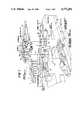
- FIG. 1is an exploded, perspective view of the arrangement of the modular components of a millimeter wave antenna interface in accordance with the present invention
- FIG. 2is a perspective view of a broken away portion of an RF chip module
- FIG. 3is a bottom view of an RF chip module shown at 10 in FIG. 1;
- FIG. 4is a sectional view of module 10 taken along lines A-A' of the bottom view shown in FIG. 3;
- FIG. 5is a sectional view of the module 10 taken along lines B-B' of the bottom view shown in FIG. 3.
- each RF chip module 10may house a plurality of (e.g. four) microwave integrated circuit (e.g.
- GaAsGaAs chips containing amplifiers, controlled phase shift/switching networks and microwave emitter elements, (shown schematically at 10A, 10E in FIG. 2) such as chips manufactured by Hughes Aircraft Company which operate over a frequency bandwidth of 43 to 45 GHz. (It is to be understood, of course, that the invention is not limited to the use of this particular chip or the frequency range of its operation.)
- each RF module 10contains a plurality of (gallium arsenide) monolithic microwave integrated circuit chips 161 preferably arranged in a side-by-side cluster on the top surface 188 of a multilayer ceramic (e.g. cofired aluminum oxide) chip carrier package, comprised of a first or upper ceramic layer 185 formed on the top surface 189 of a second ceramic substrate layer 186.
- the ceramic packageis hermetically sealed by a cover (shown at 11 in FIGS. 4 and 5 to be described supra, but not illustrated in FIG. 2 in order to show the details of the module's interior).
- Each microwave integrated circuit chipcontains a plurality of input/output signal coupling ports 163 and an RF signal coupling port 160.
- the upper ceramic substrate layer 185 to which the array of chips 161 is bondedprovides a stress tolerant support backing carrier for the chips 161, while the second ceramic substrate layer 186 forms an additional layer of mechanical support and also provides an interconnect structure that permits the closely spaced signal coupling ports on the edges of the chips to be mechanically externally accessible.
- a diverging or fan-out arrangement of input/output signal conductor layers or conductor traces 166is formed on the top surface 189 of the lower ceramic substrate layer 186.
- First ends of layers 166are connected, as by way of a suitable conductive paste (such as tungsten or molybdenum-manganese paste), to the bottoms of solid post vias 165 which extend through apertures 164 in the upper ceramic substrate layer 185.
- Second ends of links 166are similarly connected to the tops of a set of solid post vias 167 which are provided in spaced apart apertures 168 in the lower ceramic substrate 186 and are contiguous with bonding pads 171 on the bottom surface 101 of substrate layer 186, as shown in FIG. 3.
- the apertures 164 of substrate layer 185 in which the solid post vias 165 are formedare aligned with and disposed adjacent to the input/output signal coupling ports 163 disposed along the edges of the chips 161 and are wire or ribbon-bonded thereto as shown at 162.
- the physical spacing between signal coupling ports 163 of the RF chips 161makes it practically unfeasible to connect external coupling pin directly to these locations.
- the distribution of signal conductor layers 166 on the top surface 189 of the lower ceramic substrate layer 186permits the separation between signal coupling pins to be sufficiently large to permit a practical mechanical connection.
- a plurality of input/output signal pins 102may be bonded to pads 171 (through the use, for example, of a silver or copper eutectic braze).
- the center-to-center spacing of pins 102(each of which may have an outer diameter on the order of 16 mils) may be on the order of 75 mils, which is considerably larger and therefore mechanically preferable from an interconnect and handling standpoint than the spacing between signal coupling ports 163 of chips 161 which is typically only on the order of 35 mils.
- signal conductor layers 166also permit the location of pins 102 to be physically spaced apart from the locations of signal coupling ports 163 by a distance sufficient to accommodate the placement of a baseplate 107 made of heat dissipating and electrically conductive material (such as Kovar or copper-tungsten alloy) on the bottom surface 101 of lower ceramic substrate 186.
- baseplate 107has a somewhat rectangular "S"-shaped configuration with the perimeter 121 thereof accommodating the disposition of respective pluralities of input/output signal pins 102 at spaced apart regions 110 and 120, adjacent to that portion of the bottom surface 101 of module 10 whereat the baseplate 107 is affixed, while still occupying a sufficient portion of the area of the bottom surface 101 of substrate layer 186 to provide substantial heat dissipation therethrough.
- each RF module 10contains a pair of RF signal coupling ports comprised of center conductors 105/106 which extend through respective concentric cylindrical apertures 115/116 in ceramic substrate layers 185 and 186 and metallic baseplate 107.
- each RF transmission line apertureis filled with a glass dielectric layer (e.g. Corning 7072 or 7052 sealing glass) 183/184 so as to as define a coaxial transmission line have a characteristic impedance compatible with the RF signal coupling ports of chips 161 (e.g. 50 ohms).
- the top or interior end of each of center conductor pins 105 and 106may be wire-bonded, as at 118, to RF signal pad 160 on chip 161.
- conductor pin 105may be connected at its interior end portion to the RF signal coupling ports of spaced apart gallium arsenide chips 161A and 161B.
- center conductor pin 106may be connected to the RF signal coupling ports of gallium arsenide chips 161C and 161D.
- pins 105 and 106provide a power split between the RF signal coupling ports of two adjacent gallium arsenide chips (161A, 161B and 161C, 161D).
- the impedance characteristics of the connection between the center conductor pin 105/106 and the RF signal ports of the gallium arsenide chipsmay be tailored in the manner described in copending application Ser. No. 888,934 filed July 24, 1986 entitled "Plug-In Package for High Speed Microwave Integrated Circuits" by D. E. Heckaman et al and assigned to the Assignee of the present application.
- each module 10is further provided with a mechanical coupling connection comprised of a retaining post 135, having an interior threaded bore 191 and a pair of spaced apart guide posts 131 and 132, each of which extends from the bottom surface 109 of metallic baseplate 107.
- Guide posts 131 and 132are aligned with apertures (421/422, respectively, as shown in FIG. 1) in the coldplate/waveguide structure to which the modules are to be attached and have a length which exceeds the length of input/output pins 102 and RF center conductor pins 105 and 106.
- Retaining post 135is insertable (along axis 141) into a cylindrical bore 441 (FIGS. 1 and 4) provided in the underlying coldplate/waveguide structure and is affixed thereto by a retaining screw 137 (FIG. 4) inserted from a bottom bore 150 of the coldplate/waveguide structure and threaded into engagement with the interior threaded bore 191 of retaining post 135.
- Compliant socket carrier 20contains a plurality of pin sockets 201 which extend beneath bottom surface 211 and are adapted to receive and engage the pluralities of input/output pins 102/103 of module 10 and to be interconnected with conductive apertures in printed wiring board 30 to which the interconnection links retained therein extend.
- the outer perimeter of compliant socket carrier 20is shaped to conform with the substantially rectangular S-shaped perimeter 121 of metallic baseplate 107 and with the rectilinear outer edges of module 10.
- Compliant socket carrier 20has a top surface 205 which is disposed adjacent to the bottom surface 101 of ceramic substrate layer 186 of module 10 when the pins 102/103 of RF module 10 engage the pin sockets 201 of carrier 20, as shown in FIG. 5.
- the pin sockets 201 of socket carrier 20are distributed in a pattern corresponding to the pattern of input/output signal pins 102/103 of module 10 and with a plurality of conductive apertures 311 of multilayer printed wiring board 30.
- printed wiring board 30is of conventional construction and includes a plurality of signal conductor tracks formed therein for intercoupling supply voltage levels and control signals to the input/output signal pin sockets 201 and thereby to the pins 102/103 of the RF module 10.
- the signal conductor links of printed wiring board 30preferably extend to a multicable connector at a side edge portion of the printed wiring board 30 to which a suitable signal connector cable may be coupled.
- the conductor highways of the printed wiring board 30 and the cable connectorare not shown in the drawings in order to facilitate the illustration of the components of the invention.
- multilayer printed wiring board 30is mechanically configured to contain a plurality of rectangular "S" shaped slots or apertures 301 which extend completely through the printed wiring board between respective top and bottom surfaces 302 and 303 thereof. Slots 301 are of substantially the same size and shape as a plurality of rectangular S-shaped thermal pillars 401 which are formed in an upper portion of coldplate/waveguide element 40.
- multilayer printed wiring board 30also contains a plurality of conductive pin receiving apertures 311 to which the sockets 201 of socket carrier 20 are connected when the socket carrier is inserted into the multilayer printed wiring board 30.
- the thickness of the printed wiring board 30 and that of the socket carrier (including connector pins 201)are such that, when placed together, their combined thickness is no greater than the height of the thermal pillars 401 of coldplate/waveguide element 40, as shown in FIG. 5.
- thermal pillars 401 of coldplate/waveguide element 40are defined by a plurality of depressions 406, having sidewalls 405 which correspond to the sidewalls of the pillars 401, and floors 407.
- the height or depth of each thermal pillaris defined between the top surface 471 thereof and floor 407.
- the sidewalls of each thermal pillar 401have a rectangular S-shaped perimeter which effectively conforms with the rectangular S-shape (FIG. 3) of the sidewalls or perimeter 121 of metallic baseplate 107 of each RF module 10.
- each thermal pillar 401also includes a cylindrical bore 441 extending therethrough and sized to accommodate retaining post 135 of RF module 10.
- Each thermal pillaralso includes respective apertures 421 and 422 positioned and size to accommodate guide posts 131 and 132 of module 10 and an additional pair of apertures 431 and 432 containing respective RF transmission line connection sockets 461 and 462 to which the center conductor pins 105 and 106 of the RF module are to be connected (FIG. 4).
- sockets 461 and 462, apertures 421 and 422 and cylindrical bore 441are aligned with the corresponding mating electrical and mechanical connection elements on the bottom surface of each RF module, such that the rectangular "S"-shape of bottom plate 107 of module 10 is in substantial alignment with the rectangular "S"-shape of thermal pillar 461.
- FIGS. 4 and 5The manner in which the RF module 10, compliant socket carrier 20 and printed wiring board 30 are stacked and connected together and retained by coldplate/waveguide element 40 is shown in FIGS. 4 and 5.
- retaining post 135 of RF module 10is insertable into bore 441 of a thermal pillar 401 and is engaged at the interior threaded bore portion 191 thereof by a retaining screw 137 which is insertable through a slot 150 in the opposite side of coldplate/waveguide element 40 such that the head 138 of screw 137 engages a land portion 140 extending to an interior bore 133 through which the shaft of the threaded bolt 137 passes.
- RF module 10is drawn toward coldplate/waveguide element 40 until the bottom surface 109 of baseplate 107 engages the top surface 471 of thermal pillar 401.
- the RF module 10, compliant socket carrier 20 and printed wiring board 30are securely retained by and electrically and thermally connected with coldplate/waveguide element 40.
- the physical dimensions of depressions 406 and thermal pillars 401are such as to permit a physical packaging of modules 10 immediately adjacent to one another as shown in FIGS. 4 and 5 and by the broken line illustration in FIG. 1 of a non-detailed RF module 10'.
- the top surface portion of the coldplate/waveguide element 40contains the above-described pattern of depressions 406 and thermal pillars 401, interconnection of the input/output signal pins 102/103 of the RF modules 10 to the external world can take place easily without the necessity of providing a complicated interface through an underlying waveguide structure which is used to feed the RF pins 105/106.
- input/output signal connections to the modules 10are accommodated via cable connections at the sides of the printed wiring board 30.
- interfacing of the RF pins 105/106is readily accommodated by a pair of coaxial RF socket connector pin shown in detail in FIG. 4.
- each thermal pillar 401has a pair of cylindrical apertures 431 and 432 respectively coaxially aligned with the axes of center pins 105 and 106 of each RF module 10.
- Each aperture 431 and 432contains therein an RF socket 461 and 462, respectively, having an internal cylindrical dielectric sleeve 361/362 (such as a Teflon tube) within which a conductive compliant spring sleeve element 468/469 is inserted.
- the inner diameter of sleeve 468/469 when fully matedcorresponds to the outer diameter of pins 105/106 and the outer diameter of a coaxial cable center conductor 481/482.
- a transition washer 451/452is provided at the bottom of each of apertures 431 and 432 .
- each washerhas an interior bore which permits the passage of the center conductor pins that are to be joined by way of the sockets 461/462, respectively.
- the center conductor pins 481/482 of coaxial cable elements 491/492are surrounded by a dielectric outer sleeve 483/485, extending through respective cylindrical bores 487/488 from the bottom surface 472 of coldplate/waveguide element 40 to apertures 431/432 of sockets 461/462.
- the bottom portion of the coldplate/waveguide element 40is grooved or slotted to form a portion of a ridged waveguide power divider structure 464 to which the center pins 481/482 of the coaxial cable connectors extend, so as to electrically interface the RF ports of the microwave integrated circuit chips to waveguide structure defined between the coldplate/waveguide elements 40 and the top surface 571 of transition and load plate element 50.
- Element 50contains feed through apertures (not shown) for interfacing the ridged waveguide structure 464 with a rectangular waveguide structure 621 formed between the bottom surface 572 of element 50 and slots or grooves formed in bottom waveguide plate 60. As shown in FIG.
- the rectangular waveguide-forming grooves in element 60have respective parallel sidewalls 631 and 633 and a bottom wall or floor portion 632 which is parallel to the surface 572 of plate 50 against which the top surface 671 of bottom plate element 60 is placed.
- Bottom plate 60is shown having a bottom surface 672.
- the distribution of rectangular waveguides 621 in bottom plate element 60may for example, form a 64:1 powder divider to which an original output signal to be delivered to the emitter elements of the microwave chips is supplied. As the configuration and operation of such waveguide power divider structure is conventional and is not necessary for an understanding of the present invention no further details will be given here.
- the rectangular waveguide structure 621 formed in element 60serves to distribute a signal to be launched with an intended power distribution from a multiarray antenna.
- a second layer of power distributionis accomplished by the ridged waveguide 464 defined between top surface 571 of transition and load plate element 50 and the side walls of the grooves through which the ridged waveguide structure 464 is formed in the bottom surface 472 of coldplate/waveguide element 40.
- the configuration of the ridged waveguide structure 464may comprise an arrangement of 64 8:1 power dividers feeding the respective emitter elements of the chips contained in modules 10 through the transmission line center conductor pins 481/482, extending therebetween, as described supra.
- the module support structure of the present inventionprovides considerable heat dissipation for the RF module 10. Additional cooling is provided by a plurality of coolant channels 451 formed in coldplate/waveguide element 40, through which a cooling fluid may pass for augmenting the heat dissipation characteristics of the structure.
- the present inventionprovides a packaging mechanism for housing a plurality of high frequency monolithic integrated circuit chips that not only ruggedizes the signal interface connectors but provides substantial heat dissipation and avoids complex hardware constraints of conventional packaging arrangements where all signal interface ports are derived from the same side of the packaging structure.
- the printed wiring board structurethrough which chip control signals are supplied, may be disposed in substantially the immediately adjacent vicinity of the RF modules, rather than being placed in the vicinity of the waveguide structure which creates the practical problem of a dual interface across the thickness of the mounting hardware.
- Input/output signalscan be extracted at the side of the printed wiring boards away from the ports whereat RF signals are interconnected with the waveguide structure of rectangular waveguide element. This also permits a simplified interconnection scheme comprised of coaxial transmission line connector pins in direct alignment with the RF connectors of each RF module and the waveguide structure therebeneath.
Landscapes
- Engineering & Computer Science (AREA)
- Physics & Mathematics (AREA)
- Condensed Matter Physics & Semiconductors (AREA)
- General Physics & Mathematics (AREA)
- Computer Hardware Design (AREA)
- Microelectronics & Electronic Packaging (AREA)
- Power Engineering (AREA)
- Manufacturing & Machinery (AREA)
- Non-Reversible Transmitting Devices (AREA)
Abstract
Description
The present invention relates in general to microwave signal coupling devices and is particularly directed to an arrangement for interfacing extremely high frequency antenna elements incorporated with monolithic integrated circuit devices to external signal coupling ports.
Signal distribution networks, particularly those employed with large signal transmission distances, (e.g. radio wave launch devices) typically contain one or more stages of amplification to ensure sufficient power levels at signal reception and recovery sites. In RF signal transmission systems, power distribution from a modulation source to the antenna emitter elements has conventionally been effected by the use of a source amplifier stage the output of which is coupled through a signal distribution network, e.g. waveguide, stripline, to one or more RF emitters. With the continuing increase in the transmitted carrier frequency and improved microwave integrated circuit devices, however, customary approaches to interfacing successive stages of a network may no longer provide an adequate means for RF and low frequency signals to be practically integrated. This is especially true of beam steering transmission type phased array antennas operating in the mm-wave or near mm-wave portion of the RF spectrum.
More particularly, because many of these antennas must be capable of scanning over large angles, constraints imposed on the generation of large grating lobes restricts the emitter element spacing typically to one-half of the free space wavelength. As a result, the integration density of microwave integrated circuit devices employed in the design of these antennas becomes increasingly higher. Where transistors and phase shifters are present, the process of incorporating both high frequency RF, D.C. power and control signals within a single scheme, which provides for large thermal dissipation (owing to the relative inefficiency of current GaAs FETs at mm-wave frequencies), becomes increasingly difficult to implement in a practical manner where the high frequency RF distribution and interfacing is concerned, dimensional tolerances of the physical structure in which the devices are contained become critical design/performance parameters. Consequently, both the length and physical characteristics of signal runs between components may significantly affect (degrade) interstage coupling/impedance characteristics of a network. Small dimensional irregularities at a signal coupling transition may influence the degree to which residual capacitance and inductance are present, causing large variations in input or output impedance at the signal coupling interface. Such constraints are especially critical in compact multielement antenna arrays, as may be employed in high performance military aircraft, where the conventional approach of using an inherently lossy branched conductor network to distribute power from single signal power source suffers unacceptable attenuation.
To obviate this drawback of substantial signal loss through the signal distribution network, antenna arrays employing monolithic integrated RF amplifier/emitter components (namely-those with the power amplifier at the emitter site by making both amplifier and antenna emitter reside within the same high speed semiconductor (GaAs) chip) have been proposed. Because of their microminiaturized circuit structure and the above-described signal transmission link limitations, the physical dimensions of signal coupling ports for interfacing such chips with other signal processing hardware have limited their incorporation in large antenna arrays. Moreover, as the density and volume of the array increases, heat dissipation, which is an especially acute requirement for GaAs FETs operating at K-band and above, becomes a significant hardware packaging consideration.
In accordance with the present invention, there is provided a new and improved signal interface/packaging arrangement for physically and electronically supporting a plurality of high circuit density/high (signal processing) speed monolithic microwave integrated circuit components in a large density array structure that is compact, and therefore readily adaptable to complex environment (e.g. high performance aircraft/spacecraft) applications, affords efficient thermal dissipation and provides a practical interconnect mechanism between the signal coupling ports of each chip and the external world. For this purpose, the present invention embodies a laminated arrangement of a multi RF chip module, a compliant socket carrier, interconnect wiring board and heat dissipating cold plate/waveguide structure.
The multi RF chip module is formed of a first layer of ceramic substrate upon top surface of which a plurality of high frequency (e.g. gallium arsenide) monolithic integrated circuit chips, containing signal amplification, phase shift networks, etc. and antenna emitter elements, are disposed. As a result of conditions mentioned earlier which serve to limit the emitter spacing, and the need to minimize proximity of adjacent circuit elements due to RF coupling, the chips are arranged immediately adjacent to one another and have their signal coupling ports disposed along the outer peripheries thereof. Solid post vias, wirebond-connected to input/output signal coupling ports of the chips, extend through apertures in the first substrate layer to fan-out conductor trace patterns on the top surface of a second ceramic substrate layer. The respective conductor traces of the pattern on the second substrate layer extend to spaced apart locations whereat input/output signal pins are disposed. The input/output signal pin locations on the second substrate layer are spaced apart sufficiently to facilitate physical handling and interfacing with feed-through connectors of the compliant pin socket carrier. RF signal coupling ports of the modules are formed by a pair of center conductor pins wirebond-connected to the chips and extending through respective coaxial cylindrical apertures in the first and second ceramic substrate layers. The walls of the respective apertures are conductive so as to form transmission line ground planes for the center conductor pins extending therethrough.
Affixed to the bottom surface of the second ceramic substrate layer is a metallic baseplate, which provides a heat dissipation path away from the ceramic substrate layers (and the chips mounted thereon) and forms an extension of the ground planes for the center conductor pins of the RF signal coupling ports by way of apertures therethrough aligned with the conductive-walled apertures of the first and second substrate layers. In addition, the baseplate also serves as a structural support element for the ceramic portion of the module, minimizing strain of the non-complaint ceramic resulting from loads generated during attachment of the module to the coldplate. The baseplate is shaped to have a perimeter that lies within the distribution of the input/output signal pins extending from the bottom of the second ceramic substrate layer. The lengths of the input/output signal pins and the center conductor pins of the RF signal coupling ports exceed the thickness of the baseplate. Each module is also provided with a pair of spaced-apart alignment guide posts which extend from the baseplate, and a retaining port through which the module is to be mounted to an underlying cold plate/waveguide structure. The lengths of the guide posts and the retaining post exceed the lengths of the pins so as to ensure mechanical alignment of the pins, primarily the RF center conductor pins, prior to their connection with adjacent interface components.
The coldplate/waveguide structure is a laminated structure comprising a top metallic coldplate element, an interior metallic waveguide transition and load plate element and a bottom metallic waveguide plate element. The coldplate element has a top surface portion in which an arrangement of depressions is provided. Between the depressions, land portions or pillars are defined. The perimeter of each pillar is shaped to effectively conform with the shape of the metallic baseplate of an RF chip module to be placed in contact therewith. Each pillar has a central aperture for receiving the retaining post of a module and a pair of guide post apertures for properly aligning the RF chip module when the module is placed on the pillar. Additional apertures extend through each pillar in alignment with the center conductor pins of the RF signal ports of the RF chip module and contain transmission line feed through sockets which interface the center conductor pins of the RF modules with coaxial pin connector links that are coupled to a ridged waveguide power divider structure defined between the bottom surface of the coldplate element and the top surface of the interior waveguide transition and load plate element therebeneath.
The printed wiring board contains a distributed pattern of interconnect wiring layers which extend to cable connector elements on the side of the board and thereby serve to connect the input/output signal pins of the modules to the outside world. Physical and electrical interfacing of the input/output signal pins of the modules and the printed wiring board is effected by way of the compliant socket carrier inserted between. To enable the printed wiring board to be compactly physically integrated with the coldplate/waveguide structure, the board is configured to have a distribution of slots therethrough shaped to conform with the sidewalls of the pillars of the coldplate element so that, when placed on the coldplate element, the wiring board drops into the depressions and is securely confined by the pillars.
A plurality of compliant socket carriers, each of which is also shaped to match the shape of a depression in the coldplate element, is placed in the depressions of the coldplate/waveguide structure between the bottom surfaces of the RF chips modules and the top surface of the printed wiring board, and serves to guide and interface the input/output signal pins of the RF chip modules with signal interconnect layers of the printed wiring board.
The interior of the coldplate element beneath the depressions is provided with an arrangement of coolant channels. The bottom surface of the coldplate element is shaped or grooved to define a ridged waveguide cavity power divider structure the walls of which are formed by the side and bottom walls of the grooves in the coldplate element and the top surface of the waveguide transition and load plate element placed thereagainst. As described above, the center conductor pins of the RF signal coupling ports of the chip carrier modules are coupled to transmission line connectors which extend through apertures in the coldplate element to the ridged waveguide cavity structure.
The top surface of the bottom waveguide plate element also has a set of grooves the walls of which define the bottom wall and opposite sidewalls of a rectangular waveguide power divider structure. The flat bottom surface of the transition plate forms the top surface of the rectangular waveguide power divider structure. A matrix of interface feed through transitions is formed through the transition plate element to interface the ridged waveguide power divider structure formed between the top of the transition plate element and the bottom of the coldplate element with the rectangular waveguide power divider structure formed between the bottom of the transition plate element and the top of the underlying bottom waveguide plate element.
FIG. 1 is an exploded, perspective view of the arrangement of the modular components of a millimeter wave antenna interface in accordance with the present invention;
FIG. 2 is a perspective view of a broken away portion of an RF chip module;
FIG. 3 is a bottom view of an RF chip module shown at 10 in FIG. 1;
FIG. 4 is a sectional view ofmodule 10 taken along lines A-A' of the bottom view shown in FIG. 3; and
FIG. 5 is a sectional view of themodule 10 taken along lines B-B' of the bottom view shown in FIG. 3.
Referring now to FIG. 1, there is shown, in perspective, an exploded view of the overall structural configuration a module interface for a monolithic millimeter wave antenna array in accordance with the present invention. The antenna itself is comprised of an array of RF chip modules (10') (only one of which is fully illustrated in FIG. 1 in order to simplify the drawing), containing a plurality of microwave integrated circuit signal processing and radiating components that are to be interfaced with external signal coupling ports through which operation of the antenna array is controlled and monitored. For this purpose, eachRF chip module 10 may house a plurality of (e.g. four) microwave integrated circuit (e.g. GaAs) chips containing amplifiers, controlled phase shift/switching networks and microwave emitter elements, (shown schematically at 10A, 10E in FIG. 2) such as chips manufactured by Hughes Aircraft Company which operate over a frequency bandwidth of 43 to 45 GHz. (It is to be understood, of course, that the invention is not limited to the use of this particular chip or the frequency range of its operation.)
As shown in detail in FIG. 2, eachRF module 10 contains a plurality of (gallium arsenide) monolithic microwave integratedcircuit chips 161 preferably arranged in a side-by-side cluster on thetop surface 188 of a multilayer ceramic (e.g. cofired aluminum oxide) chip carrier package, comprised of a first or upperceramic layer 185 formed on thetop surface 189 of a secondceramic substrate layer 186. The ceramic package is hermetically sealed by a cover (shown at 11 in FIGS. 4 and 5 to be described supra, but not illustrated in FIG. 2 in order to show the details of the module's interior). Each microwave integrated circuit chip contains a plurality of input/outputsignal coupling ports 163 and an RFsignal coupling port 160. Because of the extremely close spacing of the circuit components and associated interconnect links on the integrated circuit chips, direct mechanical coupling of signal interface connectors to the circuitry of the chips cannot be realized without the use of extremely fragile hardware components and without possibly damaging the highly brittle structure of the gallium arsenide chips. In accordance with the present invention, the upperceramic substrate layer 185 to which the array ofchips 161 is bonded provides a stress tolerant support backing carrier for thechips 161, while the secondceramic substrate layer 186 forms an additional layer of mechanical support and also provides an interconnect structure that permits the closely spaced signal coupling ports on the edges of the chips to be mechanically externally accessible.
For this purpose, a diverging or fan-out arrangement of input/output signal conductor layers orconductor traces 166 is formed on thetop surface 189 of the lowerceramic substrate layer 186. First ends oflayers 166 are connected, as by way of a suitable conductive paste (such as tungsten or molybdenum-manganese paste), to the bottoms ofsolid post vias 165 which extend throughapertures 164 in the upperceramic substrate layer 185. Second ends oflinks 166 are similarly connected to the tops of a set ofsolid post vias 167 which are provided in spaced apartapertures 168 in the lowerceramic substrate 186 and are contiguous withbonding pads 171 on thebottom surface 101 ofsubstrate layer 186, as shown in FIG. 3. Theapertures 164 ofsubstrate layer 185 in which thesolid post vias 165 are formed are aligned with and disposed adjacent to the input/outputsignal coupling ports 163 disposed along the edges of thechips 161 and are wire or ribbon-bonded thereto as shown at 162. As noted above, the physical spacing betweensignal coupling ports 163 of the RF chips 161 makes it practically unfeasible to connect external coupling pin directly to these locations. Pursuant to the invention, the distribution of signal conductor layers 166 on thetop surface 189 of the lowerceramic substrate layer 186 permits the separation between signal coupling pins to be sufficiently large to permit a practical mechanical connection. For this purpose, a plurality of input/output signal pins 102 may be bonded to pads 171 (through the use, for example, of a silver or copper eutectic braze). The center-to-center spacing of pins 102 (each of which may have an outer diameter on the order of 16 mils) may be on the order of 75 mils, which is considerably larger and therefore mechanically preferable from an interconnect and handling standpoint than the spacing betweensignal coupling ports 163 ofchips 161 which is typically only on the order of 35 mils.
In addition to providing a mechanism for practically connecting thesignal coupling ports 163 withexternal pins 102, signal conductor layers 166 also permit the location ofpins 102 to be physically spaced apart from the locations ofsignal coupling ports 163 by a distance sufficient to accommodate the placement of abaseplate 107 made of heat dissipating and electrically conductive material (such as Kovar or copper-tungsten alloy) on thebottom surface 101 of lowerceramic substrate 186.
The manner in which such ametallic baseplate 107 is arranged on thebottom surface 101 ofmodule 10 is illustrated in FIG. 3. As shown therein,baseplate 107 has a somewhat rectangular "S"-shaped configuration with theperimeter 121 thereof accommodating the disposition of respective pluralities of input/output signal pins 102 at spaced apartregions bottom surface 101 ofmodule 10 whereat thebaseplate 107 is affixed, while still occupying a sufficient portion of the area of thebottom surface 101 ofsubstrate layer 186 to provide substantial heat dissipation therethrough.
In addition to the spaced apart pluralities of input/output signal pins 102, eachRF module 10 contains a pair of RF signal coupling ports comprised ofcenter conductors 105/106 which extend through respective concentriccylindrical apertures 115/116 in ceramic substrate layers 185 and 186 andmetallic baseplate 107. As shown in FIG. 2 and in further detail in FIG. 4, which is a sectional view taken along line A-A' of FIG. 3, eachcylindrical aperture 115/116 which is formed through ceramic substrate layers 185 and 186 and throughmetallic base plate 107, has a conductive cylindricalouter wall portion 181/182 (such as a Kovar conductor layer) which extends from thetop surface 188 ofceramic substrate 185 to thebottom surface 109 ofbaseplate 107. Between thecenter conductor 105/106 andcylindrical wall portion 181/182, each RF transmission line aperture is filled with a glass dielectric layer (e.g. Corning 7072 or 7052 sealing glass) 183/184 so as to as define a coaxial transmission line have a characteristic impedance compatible with the RF signal coupling ports of chips 161 (e.g. 50 ohms). The top or interior end of each of center conductor pins 105 and 106 may be wire-bonded, as at 118, toRF signal pad 160 onchip 161. In the bottom view of anRF module 10 shown in FIG. 3,conductor pin 105 may be connected at its interior end portion to the RF signal coupling ports of spaced apartgallium arsenide chips center conductor pin 106 may be connected to the RF signal coupling ports ofgallium arsenide chips 161C and 161D. In other words, pins 105 and 106 provide a power split between the RF signal coupling ports of two adjacent gallium arsenide chips (161A, 161B and 161C, 161D). The impedance characteristics of the connection between thecenter conductor pin 105/106 and the RF signal ports of the gallium arsenide chips may be tailored in the manner described in copending application Ser. No. 888,934 filed July 24, 1986 entitled "Plug-In Package for High Speed Microwave Integrated Circuits" by D. E. Heckaman et al and assigned to the Assignee of the present application.
In addition to the signal interconnection mechanism provided by way of input/output signal pins 102 and RF transmission line center conductor pins 105 and 106, eachmodule 10 is further provided with a mechanical coupling connection comprised of a retainingpost 135, having an interior threaded bore 191 and a pair of spaced apart guideposts bottom surface 109 ofmetallic baseplate 107. Guide posts 131 and 132 are aligned with apertures (421/422, respectively, as shown in FIG. 1) in the coldplate/waveguide structure to which the modules are to be attached and have a length which exceeds the length of input/output pins 102 and RF center conductor pins 105 and 106. Retainingpost 135 is insertable (along axis 141) into a cylindrical bore 441 (FIGS. 1 and 4) provided in the underlying coldplate/waveguide structure and is affixed thereto by a retaining screw 137 (FIG. 4) inserted from abottom bore 150 of the coldplate/waveguide structure and threaded into engagement with the interior threaded bore 191 of retainingpost 135.
Referring again to FIG. 1 and to FIGS. 4 and 5 the overall interface structure as shown as including acompliant socket carrier 20, a multilayer printedwiring board 30, a coldplate/waveguide element 40, a waveguide transition andload plate element 50 and a bottomwaveguide plate element 60.Compliant socket carrier 20 contains a plurality ofpin sockets 201 which extend beneathbottom surface 211 and are adapted to receive and engage the pluralities of input/output pins 102/103 ofmodule 10 and to be interconnected with conductive apertures in printedwiring board 30 to which the interconnection links retained therein extend. The outer perimeter ofcompliant socket carrier 20 is shaped to conform with the substantially rectangular S-shapedperimeter 121 ofmetallic baseplate 107 and with the rectilinear outer edges ofmodule 10.Compliant socket carrier 20 has atop surface 205 which is disposed adjacent to thebottom surface 101 ofceramic substrate layer 186 ofmodule 10 when thepins 102/103 ofRF module 10 engage thepin sockets 201 ofcarrier 20, as shown in FIG. 5.
Thepin sockets 201 ofsocket carrier 20 are distributed in a pattern corresponding to the pattern of input/output signal pins 102/103 ofmodule 10 and with a plurality ofconductive apertures 311 of multilayer printedwiring board 30. Except for its shape, printedwiring board 30 is of conventional construction and includes a plurality of signal conductor tracks formed therein for intercoupling supply voltage levels and control signals to the input/outputsignal pin sockets 201 and thereby to thepins 102/103 of theRF module 10. The signal conductor links of printedwiring board 30 preferably extend to a multicable connector at a side edge portion of the printedwiring board 30 to which a suitable signal connector cable may be coupled. The conductor highways of the printedwiring board 30 and the cable connector are not shown in the drawings in order to facilitate the illustration of the components of the invention.
As mentioned above, the wiring tracks are of conventional multilayer configuration within thewiring board 30. Uniquely, however, multilayer printedwiring board 30 is mechanically configured to contain a plurality of rectangular "S" shaped slots orapertures 301 which extend completely through the printed wiring board between respective top andbottom surfaces Slots 301 are of substantially the same size and shape as a plurality of rectangular S-shapedthermal pillars 401 which are formed in an upper portion of coldplate/waveguide element 40. As noted supra, multilayer printedwiring board 30 also contains a plurality of conductivepin receiving apertures 311 to which thesockets 201 ofsocket carrier 20 are connected when the socket carrier is inserted into the multilayer printedwiring board 30. The thickness of the printedwiring board 30 and that of the socket carrier (including connector pins 201) are such that, when placed together, their combined thickness is no greater than the height of thethermal pillars 401 of coldplate/waveguide element 40, as shown in FIG. 5.
As shown in FIG. 1,thermal pillars 401 of coldplate/waveguide element 40 are defined by a plurality ofdepressions 406, havingsidewalls 405 which correspond to the sidewalls of thepillars 401, andfloors 407. The height or depth of each thermal pillar is defined between thetop surface 471 thereof andfloor 407. The sidewalls of eachthermal pillar 401 have a rectangular S-shaped perimeter which effectively conforms with the rectangular S-shape (FIG. 3) of the sidewalls orperimeter 121 ofmetallic baseplate 107 of eachRF module 10. As a result, when thebottom surface 109 ofbaseplate 107 of amodule 10 is placed in contact with thetop surface 471 of athermal pillar 401, the heat dissipation area of thebottom surface 109 of themetallic baseplate 107 of theRF module 10 encounters a corresponding heat dissipation surface area ofthermal pillar 401.
As described above, eachthermal pillar 401 also includes acylindrical bore 441 extending therethrough and sized to accommodate retainingpost 135 ofRF module 10. Each thermal pillar also includesrespective apertures guide posts module 10 and an additional pair ofapertures line connection sockets 461 and 462 to which the center conductor pins 105 and 106 of the RF module are to be connected (FIG. 4). The location ofsockets 461 and 462,apertures cylindrical bore 441 are aligned with the corresponding mating electrical and mechanical connection elements on the bottom surface of each RF module, such that the rectangular "S"-shape ofbottom plate 107 ofmodule 10 is in substantial alignment with the rectangular "S"-shape of thermal pillar 461.
The manner in which theRF module 10,compliant socket carrier 20 and printedwiring board 30 are stacked and connected together and retained by coldplate/waveguide element 40 is shown in FIGS. 4 and 5. As mentioned previously, retainingpost 135 ofRF module 10 is insertable intobore 441 of athermal pillar 401 and is engaged at the interior threadedbore portion 191 thereof by a retainingscrew 137 which is insertable through aslot 150 in the opposite side of coldplate/waveguide element 40 such that thehead 138 ofscrew 137 engages aland portion 140 extending to aninterior bore 133 through which the shaft of the threadedbolt 137 passes. Asscrew 137 is tightened into threadedbore 191 ofpost 135,RF module 10 is drawn toward coldplate/waveguide element 40 until thebottom surface 109 ofbaseplate 107 engages thetop surface 471 ofthermal pillar 401. In this mechanical positioning state, with the printedwiring board 30 andcompliant socket carrier 20 resting in the pattern ofdepressions 406 of coldplate/waveguide element 40, theRF module 10,compliant socket carrier 20 and printedwiring board 30 are securely retained by and electrically and thermally connected with coldplate/waveguide element 40. The physical dimensions ofdepressions 406 andthermal pillars 401 are such as to permit a physical packaging ofmodules 10 immediately adjacent to one another as shown in FIGS. 4 and 5 and by the broken line illustration in FIG. 1 of a non-detailed RF module 10'.
Advantageously, because the top surface portion of the coldplate/waveguide element 40 contains the above-described pattern ofdepressions 406 andthermal pillars 401, interconnection of the input/output signal pins 102/103 of theRF modules 10 to the external world can take place easily without the necessity of providing a complicated interface through an underlying waveguide structure which is used to feed the RF pins 105/106. As described above, input/output signal connections to themodules 10 are accommodated via cable connections at the sides of the printedwiring board 30. As a result, interfacing of the RF pins 105/106 is readily accommodated by a pair of coaxial RF socket connector pin shown in detail in FIG. 4.
More particularly, eachthermal pillar 401 has a pair ofcylindrical apertures RF module 10. Eachaperture RF socket 461 and 462, respectively, having an internal cylindricaldielectric sleeve 361/362 (such as a Teflon tube) within which a conductive compliantspring sleeve element 468/469 is inserted. The inner diameter ofsleeve 468/469 when fully mated corresponds to the outer diameter ofpins 105/106 and the outer diameter of a coaxialcable center conductor 481/482. At the bottom of each ofapertures 431 and 432 atransition washer 451/452 is provided. Similarly, at the top of each aperture a dielectricinterface transition washer 455/456 is provided. Each washer has an interior bore which permits the passage of the center conductor pins that are to be joined by way of the sockets 461/462, respectively. The center conductor pins 481/482 ofcoaxial cable elements 491/492 are surrounded by a dielectricouter sleeve 483/485, extending through respectivecylindrical bores 487/488 from thebottom surface 472 of coldplate/waveguide element 40 toapertures 431/432 of sockets 461/462.
The bottom portion of the coldplate/waveguide element 40 is grooved or slotted to form a portion of a ridged waveguidepower divider structure 464 to which the center pins 481/482 of the coaxial cable connectors extend, so as to electrically interface the RF ports of the microwave integrated circuit chips to waveguide structure defined between the coldplate/waveguide elements 40 and thetop surface 571 of transition andload plate element 50.Element 50 contains feed through apertures (not shown) for interfacing the ridgedwaveguide structure 464 with arectangular waveguide structure 621 formed between thebottom surface 572 ofelement 50 and slots or grooves formed inbottom waveguide plate 60. As shown in FIG. 4, the rectangular waveguide-forming grooves inelement 60 have respectiveparallel sidewalls floor portion 632 which is parallel to thesurface 572 ofplate 50 against which thetop surface 671 ofbottom plate element 60 is placed.Bottom plate 60 is shown having abottom surface 672. The distribution ofrectangular waveguides 621 inbottom plate element 60, may for example, form a 64:1 powder divider to which an original output signal to be delivered to the emitter elements of the microwave chips is supplied. As the configuration and operation of such waveguide power divider structure is conventional and is not necessary for an understanding of the present invention no further details will be given here. Suffice it to say that therectangular waveguide structure 621 formed inelement 60 serves to distribute a signal to be launched with an intended power distribution from a multiarray antenna. A second layer of power distribution is accomplished by the ridgedwaveguide 464 defined betweentop surface 571 of transition andload plate element 50 and the side walls of the grooves through which the ridgedwaveguide structure 464 is formed in thebottom surface 472 of coldplate/waveguide element 40. For example, the configuration of the ridgedwaveguide structure 464 may comprise an arrangement of 64 8:1 power dividers feeding the respective emitter elements of the chips contained inmodules 10 through the transmission line center conductor pins 481/482, extending therebetween, as described supra.
Because of the substantial thickness of metal provided by coldplate/waveguide element 40, transition andload plate element 50 andrectangular waveguide element 60, the module support structure of the present invention provides considerable heat dissipation for theRF module 10. Additional cooling is provided by a plurality ofcoolant channels 451 formed in coldplate/waveguide element 40, through which a cooling fluid may pass for augmenting the heat dissipation characteristics of the structure.
As will be appreciated from the foregoing description, the present invention provides a packaging mechanism for housing a plurality of high frequency monolithic integrated circuit chips that not only ruggedizes the signal interface connectors but provides substantial heat dissipation and avoids complex hardware constraints of conventional packaging arrangements where all signal interface ports are derived from the same side of the packaging structure. Through the use of the distribution of depressions and thermal pillars in the coldplate/waveguide element, the printed wiring board structure, through which chip control signals are supplied, may be disposed in substantially the immediately adjacent vicinity of the RF modules, rather than being placed in the vicinity of the waveguide structure which creates the practical problem of a dual interface across the thickness of the mounting hardware. Input/output signals can be extracted at the side of the printed wiring boards away from the ports whereat RF signals are interconnected with the waveguide structure of rectangular waveguide element. This also permits a simplified interconnection scheme comprised of coaxial transmission line connector pins in direct alignment with the RF connectors of each RF module and the waveguide structure therebeneath.
While I have shown and described an embodiment in accordance with the present invention, it is understood that the same is not limited thereto but is susceptible of numerous changes and modifications as known to a person skilled in the art, and I therefore do not wish to be limited to the details shown and described herein but intend to cover all such changes and modifications as are obvious to one of ordinary skill in the art.
Claims (27)
1. An arrangement for supporting and intercoupling at least one signal processing device to signal interface ports comprising:
a device support module comprised of a substrate supporting at least one signal processing device on a first surface thereof, a plurality of input/output signal connector means disposed at a first portion of a second surface of said substrate and interconnected through said substrate to ones of signal connection ports of said at least one signal processing device, an electrically and thermally conductive plate disposed on a second portion of said second surface of said substrate adjacent to said first portion thereof, said plate having signal coupling links extending through apertures in said plate to others of said signal connection ports of said at least one signal processing device; and
means for physically attaching said module to a transmission link support structure.
2. An arrangement according to claim 1, said signal processing device comprises a monolithic microwave integrated circuit device, said signal coupling links extending through said plate include microwave signal coupling links extending through apertures therethrough to microwave signal coupling ports of said at least one microwave signal processing device, and said transmission link support structure comprises a microwave transmission link support structure, and wherein said microwave transmission link support structure comprises an electrically and thermally conductive member having a first surface thereof disposed in electrical and thermal communication with said thermally conductive plate and containing an internal distribution of waveguide elements, and means for providing respective microwave signal transmission links between microwave signal coupling links of said module and said internal distribution of waveguide elements.
3. An arrangement according to claim 2, further including an input/output signal interconnect link support member containing a plurality of input/output signal transmission links for interfacing input/output signals with the input/output signal connector means of said module and having a physical shape that enables said interconnect link support member to be disposed adjacent to said electrically and thermally conductive plate between said first portion of said second surface of said substrate and said first surface of said electrically and thermally conductive member when said electrically and thermally conductive plate is placed in electrical and thermal communication with said first surface of said electrically and thermally conductive member.
4. An arrangement according to claim 3, wherein said first surface of said electrically and thermally conductive member of said microwave transmission link support structure has a plurality of depressions formed therein, said depressions defining therebetween a plurality of pillar portions, the shapes of said pillar portions effectively accommodating the shapes of the plates of modules disposed in electrical and thermal communication therewith by being mounted atop respective ones of said pillar portions.
5. An arrangement according to claim 4, wherein said input/output signal interconnect link support member has a physical shape that enables said interconnect link support member to be disposed within the depressions of said electrically and thermally conductive member of said microwave transmission link support structure adjacent to the pillar portions thereof.
6. An arrangement according to claim 5, further comprising means, disposed between said first portion of said second surface of a respective module and said input/output signal interconnect link support member and shaped to be disposed within the depressions of said electrically and thermally conductive member of said microwave transmission link support structure, for electrically intercoupling input/output signal connector means of said module with input/output signal transmission links of said input/output signal interconnect link support member.
7. An arrangement according to claim 6, wherein said electrically intercoupling means comprises respective input/output signal pin socket carriers each having a plurality of input/output signal pin socket connectors disposed in alignment with a respective plurality of input/output signal pins of which said input/output signal connector means of said module are comprised and being mounted in a respective one of said depressions such that said socket connectors thereof electrically intercouple input/output signal pins of said module and input/output signal transmission links of said interconnect link support member.
8. An arrangement according to claim 7, wherein the combined effective thickness of a socket carrier and said interconnect link support member is no greater than the depths of said depressions.
9. An arrangement according to claim 2, wherein said electrically and thermally conductive member of said microwave transmission link support structure contains a plurality of cooling channels distributed therein through which cooling fluid may pass to assist in the cooling of said at least one monolithic microwave signal processing module.
10. An arrangement according to claim 1, wherein the substrate of said module comprises a first substrate layer having a top surface corresponding to the first surface of said substrate and supporting a plurality of monolithic signal processing devices thereon, and a second substrate layer having a top surface on which said first substrate layer is disposed and a bottom surface corresponding to the second surface of said substrate, said second substrate layer having disposed on the top surface thereof a plurality of conductor links disposed between locations of said second substrate layer in alignment with locations of input/output signal connector means at the second surface of said substrate and locations of said second substrate layer in alignment with locations whereat connections through said first substrate layer to said ones of said signal connection ports of said plurality of monolithic signal processing devices are provided.
11. An arrangement according to claim 10, wherein each of said signal coupling links comprises a center conductor pin extending through a dielectric-filled aperture in said first and second substrate layers and being connected to a microwave signal connection port of a microwave signal processing device supported on the top surface of said first substrate layer, the sidewalls of said aperture being electrically conductive and forming a ground plane for said center conductor pin.
12. An arrangement according to claim 3, wherein each module includes a plurality of guide pins extending from said plate for aligning said module with respect to a corresponding plurality of guide holes formed in said support structure and sized to receive and engage said guide pins.
13. An arrangement according to claim 12, wherein the substrate of said module comprises a first substrate layer having a top surface corresponding to the first surface of said substrate and supporting a plurality of monolithic signal processing devices thereon, and a second substrate layer having a top surface on which said first substrate layer is disposed and a bottom surface corresponding to the second surface of said substrate, said second substrate layer having disposed on the top surface thereof a plurality of conductor links disposed between locations of said second substrate layer in alignment with locations of input/output signal connector means at the second surface of said substrate and locations of said second substrate layer in alignment with locations whereat connections through said first substrate layer to said ones of said signal connection ports of said plurality of monolithic signal processing devices are provided.
14. An arrangement according to claim 13, wherein each of said microwave signal coupling links comprises a center conductor pin extending through a dielectric-filled aperture in said first and second substrate layers and being connected to a microwave signal connection port of a microwave signal processing device supported on the top surface of said first substrate layer, the sidewalls of said aperture being electrically conductive and forming a ground plane for said center conductor pin.
15. An arrangement according to claim 14, wherein said first surface of said electrically and thermally conductive member of said microwave transmission link support structure has a plurality of depressions formed therein, said depressions defining therebetween a plurality of pillar portions, the shapes of said pillar portions effectively accommodating the shapes of the plates of modules disposed in electrical and thermal communication therewith by being mounted atop respective ones of said pillar portions.
16. An arrangement according to claim 15, wherein a respective one of said pillar portions includes a plurality of microwave transmission line pin sockets into which said center conductor pins of microwave signal coupling links are insertable, said pin sockets being coupled with respective microwave signal transmission links to said internal distribution of waveguide elements.
17. An arrangement according to claim 1, wherein said monolithic microwave signal processing devices contain microwave signal amplifier and antenna emitter elements coupled thereto for amplifying and launching radio frequency signals at a frequency in excess of 20 GHz.
18. A module for supporting and intercoupling at least one signal processing device to signal interface ports external thereto comprising a substrate supporting at least one signal processing device on a first surface thereof, a plurality of input/output signal connector means located at a first portion of a second surface of said substrate and interconnected through said substrate to ones of signal connection ports of said at least one signal processing device, an electrically and thermally conductive plate disposed on a second portion of said second surface of said substrate adjacent to said first portion thereof said plate having signal coupling links extending through apertures in said plate to others of said signal connection ports of said at least one signal processing device, and means for physically attaching said substrate and said plate to a signal transmission link support structure.
19. A module according to claim 18, wherein said substrate comprises a first substrate layer having a top surface corresponding to the first surface of said substrate and supporting a plurality of monolithic signal processing devices thereon, and a second substrate layer having a top surface on which said first substrate layer is disposed and a bottom surface corresponding to the second surface of said substrate, said second substrate layer being disposed on the top surface thereof a plurality of conductor links disposed between locations of said second substrate layer in alignment with locations of input/output signal connector means at the second surface of said substrate and locations of said second substrate layer in alignment with locations whereat connections through said first substrate layer to said ones of said signal connection ports of said plurality of monolithic signal processing devices are provided.
20. A module according to claim 19, wherein said signal processing device comprises a monolithic microwave signal processing device, said signal coupling links comprise microwave signal coupling links, and said signal connection ports include microwave signal connection ports, and wherein each of said microwave signal coupling links comprises a center conductor pin extending through a dielectric-containing aperture in said first and second substrate layers and being connected to a microwave signal connection port of a microwave signal processing device supported on the top surface of said first substrate layer, the sidewalls of said aperture being electrically conductive and forming a ground plane for said center conductor pin.
21. A module according to claim 20, further comprising a plurality of guide pins extending from said plate for aligning said module with respect to a corresponding plurality of guide holes formed in a support structure to which said module is to be attached.
22. A module according to claim 21, wherein said monolithic microwave signal processing devices contain microwave signal amplifier and antenna emitter elements coupled thereto for amplifying and launching radio frequency signals at a frequency in excess of 20 GHz.
23. A structure for supporting and interfacing with signal interface ports a plurality of modules containing signal processing devices, said structure comprising an electrically and thermally conductive member having a plurality of depressions formed in a first surface thereof, said depressions defining therebetween a plurality of pillar portions, the shapes of said pillar portions effectively accommodating the shapes of prescribed portions of signal processing modules to be placed in electrical and thermal communication therewith by being mounted atop respective ones of said pillar portions, a respective pillar portion including means for mechanically attaching a module thereto and having formed therein means for providing a signal transmission link between said module and a signal interface port at a second surface of said conductive member, and wherein said depressions are shaped to accommodate therein a signal interconnect link member containing a plurality of signal conductors engageable with signal coupling ports of modules mounted on said pillar portions.
24. A structure according to claim 23, wherein said signal processing devices include microwave integrated circuit devices having microwave signal coupling port connections extending from said modules for engagement with said signal transmission link providing means of said pillar portions, said signal transmission link providing means comprising microwave transmission lines extending through said pillar portions to microwave signal coupling ports at said second surface of said conductive member.
25. A structure according to claim 24, wherein said conductive member further comprises a distribution of waveguide elements formed therein with which said microwave transmission lines are coupled.
26. A structure according to claim 24, wherein a signal interconnect link member is disposed within said depressions and wherein said microwave integrated circuit devices have a plurality of input/output signal port connections extending from said modules and being coupled to signal conductors of said link member.
27. A structure according to claim 24, further including respective input/output signal pin socket carriers each having a plurality of input/output signal pin socket connectors disposed in alignment with a respective plurality of input/output signal port connections of a module and being disposed in a respective one of said depressions such that said signal pin socket connectors thereof electrically intercouple input/output signal port connectors of said module with signal conductors of said link member.
Priority Applications (1)
| Application Number | Priority Date | Filing Date | Title |
|---|---|---|---|
| US06/905,932US4771294A (en) | 1986-09-10 | 1986-09-10 | Modular interface for monolithic millimeter wave antenna array |
Applications Claiming Priority (1)
| Application Number | Priority Date | Filing Date | Title |
|---|---|---|---|
| US06/905,932US4771294A (en) | 1986-09-10 | 1986-09-10 | Modular interface for monolithic millimeter wave antenna array |
Publications (1)
| Publication Number | Publication Date |
|---|---|
| US4771294Atrue US4771294A (en) | 1988-09-13 |
Family
ID=25421708
Family Applications (1)
| Application Number | Title | Priority Date | Filing Date |
|---|---|---|---|
| US06/905,932Expired - LifetimeUS4771294A (en) | 1986-09-10 | 1986-09-10 | Modular interface for monolithic millimeter wave antenna array |
Country Status (1)
| Country | Link |
|---|---|
| US (1) | US4771294A (en) |
Cited By (64)
| Publication number | Priority date | Publication date | Assignee | Title |
|---|---|---|---|---|
| US4945319A (en)* | 1989-07-28 | 1990-07-31 | Motorola, Inc. | High frequency impedance transformer |
| US4987425A (en)* | 1987-11-13 | 1991-01-22 | Dornier System Gmbh | Antenna support structure |
| US5019829A (en)* | 1989-02-08 | 1991-05-28 | Heckman Douglas E | Plug-in package for microwave integrated circuit having cover-mounted antenna |
| US5023624A (en)* | 1988-10-26 | 1991-06-11 | Harris Corporation | Microwave chip carrier package having cover-mounted antenna element |
| US5066999A (en)* | 1989-10-23 | 1991-11-19 | Micron Technology, Inc. | Resistor under wirebond pad |
| US5083132A (en)* | 1990-04-30 | 1992-01-21 | Matsushita Electric Works, Ltd. | Planar antenna with active circuit block |
| US5099254A (en)* | 1990-03-22 | 1992-03-24 | Raytheon Company | Modular transmitter and antenna array system |
| EP0428859A3 (en)* | 1989-10-20 | 1992-06-24 | Siemens Aktiengesellschaft | Eletric functional unit for data processing |
| US5128689A (en)* | 1990-09-20 | 1992-07-07 | Hughes Aircraft Company | Ehf array antenna backplate including radiating modules, cavities, and distributor supported thereon |
| US5173668A (en)* | 1991-04-29 | 1992-12-22 | International Business Machines Corporation | Apparatus and a method for an electrical transmission-line interface |
| US5198824A (en)* | 1992-01-17 | 1993-03-30 | Texas Instruments Incorporated | High temperature co-fired ceramic integrated phased array packaging |
| US5219377A (en)* | 1992-01-17 | 1993-06-15 | Texas Instruments Incorporated | High temperature co-fired ceramic integrated phased array package |
| US5297007A (en)* | 1990-09-19 | 1994-03-22 | Rockwell International Corporation | E/M shielded RF circuit board |
| EP0800093A1 (en)* | 1996-04-03 | 1997-10-08 | Honda Giken Kogyo Kabushiki Kaisha | Radar module and MMIC package for use in such radar module |
| US5791911A (en)* | 1996-10-25 | 1998-08-11 | International Business Machines Corporation | Coaxial interconnect devices and methods of making the same |
| EP0798209A3 (en)* | 1996-03-26 | 1998-11-18 | Lockheed Martin Corporation | Spacecraft with modular communication payload |
| US5886671A (en)* | 1995-12-21 | 1999-03-23 | The Boeing Company | Low-cost communication phased-array antenna |
| US6337661B1 (en)* | 1999-04-26 | 2002-01-08 | Hitachi, Ltd. | High frequency communication device |
| US6512431B2 (en) | 2001-02-28 | 2003-01-28 | Lockheed Martin Corporation | Millimeterwave module compact interconnect |
| US20030142024A1 (en)* | 2002-01-25 | 2003-07-31 | Carson Ronald Steven | Aircraft phased array antenna structure including adjacently supported equipment |
| US6828932B1 (en) | 2003-01-17 | 2004-12-07 | Itt Manufacutring Enterprises, Inc. | System for receiving multiple independent RF signals having different polarizations and scan angles |
| US6832049B1 (en)* | 1998-10-20 | 2004-12-14 | Fujitsu Limited | Optical Module |
| US20060017646A1 (en)* | 2004-07-21 | 2006-01-26 | Denso Corporation | Transceiver-integrated antenna |
| US20060145778A1 (en)* | 2004-12-30 | 2006-07-06 | Pleva Joseph S | Waveguide - printed wiring board (PWB) interconnection |
| US20060152406A1 (en)* | 2004-12-30 | 2006-07-13 | Leblanc Stephen P | Vehicle radar sensor assembly |
| US20090009405A1 (en)* | 2006-06-21 | 2009-01-08 | Broadcom Corporation | Integrated circuit with power supply line antenna structure and methods for use therewith |
| US20090009408A1 (en)* | 2006-06-21 | 2009-01-08 | Broadcom Corporation | Integrated circuit with bonding wire antenna structure and methods for use therewith |
| US20090085823A1 (en)* | 2005-06-06 | 2009-04-02 | Raytheon Company | Reduced inductance interconnect for enhanced microwave and millimeter-wave systems |
| US7683827B2 (en) | 2004-12-15 | 2010-03-23 | Valeo Radar Systems, Inc. | System and method for reducing the effect of a radar interference signal |
| US20110115580A1 (en)* | 2009-03-03 | 2011-05-19 | Bae Systems Information And Electronic Systems Integration Inc. | Two level matrix for embodying disparate micro-machined coaxial components |
| WO2012040376A1 (en)* | 2010-09-21 | 2012-03-29 | Texas Instruments Incorporated | Chip-to-chip communications using sub-millimeter waves and dielectric waveguide |
| US8542079B2 (en) | 2007-03-20 | 2013-09-24 | Nuvotronics, Llc | Coaxial transmission line microstructure including an enlarged coaxial structure for transitioning to an electrical connector |
| US8717124B2 (en) | 2010-01-22 | 2014-05-06 | Nuvotronics, Llc | Thermal management |
| US8742874B2 (en) | 2003-03-04 | 2014-06-03 | Nuvotronics, Llc | Coaxial waveguide microstructures having an active device and methods of formation thereof |
| US20140169486A1 (en)* | 2012-12-17 | 2014-06-19 | Waveconnex, Inc. | Modular electronics |
| US8814601B1 (en) | 2011-06-06 | 2014-08-26 | Nuvotronics, Llc | Batch fabricated microconnectors |
| US8866682B1 (en)* | 2011-05-18 | 2014-10-21 | Lockheed Martin Corporation | Composite forward coldplate for a phased array radar assembly |
| US8866300B1 (en) | 2011-06-05 | 2014-10-21 | Nuvotronics, Llc | Devices and methods for solder flow control in three-dimensional microstructures |
| US8917150B2 (en) | 2010-01-22 | 2014-12-23 | Nuvotronics, Llc | Waveguide balun having waveguide structures disposed over a ground plane and having probes located in channels |
| US8933769B2 (en) | 2006-12-30 | 2015-01-13 | Nuvotronics, Llc | Three-dimensional microstructures having a re-entrant shape aperture and methods of formation |
| US9024417B2 (en) | 2007-03-20 | 2015-05-05 | Nuvotronics, Llc | Integrated electronic components and methods of formation thereof |
| US20150288077A1 (en)* | 2011-09-16 | 2015-10-08 | International Business Machines Corporation | Phased-array transceiver |
| US9306254B1 (en) | 2013-03-15 | 2016-04-05 | Nuvotronics, Inc. | Substrate-free mechanical interconnection of electronic sub-systems using a spring configuration |
| US9306255B1 (en) | 2013-03-15 | 2016-04-05 | Nuvotronics, Inc. | Microstructure including microstructural waveguide elements and/or IC chips that are mechanically interconnected to each other |
| US9325044B2 (en) | 2013-01-26 | 2016-04-26 | Nuvotronics, Inc. | Multi-layer digital elliptic filter and method |
| US9374154B2 (en) | 2012-09-14 | 2016-06-21 | Keyssa, Inc. | Wireless connections with virtual hysteresis |
| US9379450B2 (en) | 2011-03-24 | 2016-06-28 | Keyssa, Inc. | Integrated circuit with electromagnetic communication |
| US9407311B2 (en) | 2011-10-21 | 2016-08-02 | Keyssa, Inc. | Contactless signal splicing using an extremely high frequency (EHF) communication link |
| US9426660B2 (en) | 2013-03-15 | 2016-08-23 | Keyssa, Inc. | EHF secure communication device |
| US9444523B2 (en) | 2011-06-15 | 2016-09-13 | Keyssa, Inc. | Proximity sensing using EHF signals |
| US9515859B2 (en) | 2011-05-31 | 2016-12-06 | Keyssa, Inc. | Delta modulated low-power EHF communication link |
| US9515365B2 (en) | 2012-08-10 | 2016-12-06 | Keyssa, Inc. | Dielectric coupling systems for EHF communications |
| US9553616B2 (en) | 2013-03-15 | 2017-01-24 | Keyssa, Inc. | Extremely high frequency communication chip |
| US9653796B2 (en) | 2013-12-16 | 2017-05-16 | Valeo Radar Systems, Inc. | Structure and technique for antenna decoupling in a vehicle mounted sensor |
| US20170187105A1 (en)* | 2015-12-29 | 2017-06-29 | Blue Danube Systems, Inc. | Low thermal impedance structure in a phased array |
| US20170309986A1 (en)* | 2016-04-20 | 2017-10-26 | Chih-Yuan Wang | Heat dissipater with an antenna structure |
| US9853696B2 (en) | 2008-12-23 | 2017-12-26 | Keyssa, Inc. | Tightly-coupled near-field communication-link connector-replacement chips |
| US9993982B2 (en) | 2011-07-13 | 2018-06-12 | Nuvotronics, Inc. | Methods of fabricating electronic and mechanical structures |
| US10310009B2 (en) | 2014-01-17 | 2019-06-04 | Nuvotronics, Inc | Wafer scale test interface unit and contactors |
| US10319654B1 (en) | 2017-12-01 | 2019-06-11 | Cubic Corporation | Integrated chip scale packages |
| US10497511B2 (en) | 2009-11-23 | 2019-12-03 | Cubic Corporation | Multilayer build processes and devices thereof |
| US10511073B2 (en) | 2014-12-03 | 2019-12-17 | Cubic Corporation | Systems and methods for manufacturing stacked circuits and transmission lines |
| US10847469B2 (en) | 2016-04-26 | 2020-11-24 | Cubic Corporation | CTE compensation for wafer-level and chip-scale packages and assemblies |
| US11309619B2 (en)* | 2016-09-23 | 2022-04-19 | Intel Corporation | Waveguide coupling systems and methods |
Citations (13)
| Publication number | Priority date | Publication date | Assignee | Title |
|---|---|---|---|---|
| US3500428A (en)* | 1967-08-30 | 1970-03-10 | Gen Electric | Microwave hybrid microelectronic circuit module |
| US3530229A (en)* | 1968-09-03 | 1970-09-22 | Ibm | Transmission line cable or the like and terminal connection therefor |
| US3818386A (en)* | 1967-04-03 | 1974-06-18 | Texas Instruments Inc | Solid-state modular microwave system |
| US4035807A (en)* | 1974-12-23 | 1977-07-12 | Hughes Aircraft Company | Integrated microwave phase shifter and radiator module |
| US4322778A (en)* | 1980-01-25 | 1982-03-30 | International Business Machines Corp. | High performance semiconductor package assembly |
| US4396936A (en)* | 1980-12-29 | 1983-08-02 | Honeywell Information Systems, Inc. | Integrated circuit chip package with improved cooling means |
| US4490721A (en)* | 1980-11-17 | 1984-12-25 | Ball Corporation | Monolithic microwave integrated circuit with integral array antenna |
| US4536824A (en)* | 1983-03-28 | 1985-08-20 | Goodyear Aerospace Corporation | Indirect cooling of electronic circuits |
| US4628407A (en)* | 1983-04-22 | 1986-12-09 | Cray Research, Inc. | Circuit module with enhanced heat transfer and distribution |
| US4641140A (en)* | 1983-09-26 | 1987-02-03 | Harris Corporation | Miniaturized microwave transmission link |
| US4667219A (en)* | 1984-04-27 | 1987-05-19 | Trilogy Computer Development Partners, Ltd. | Semiconductor chip interface |
| US4682270A (en)* | 1984-05-18 | 1987-07-21 | British Telecommunications Public Limited Company | Integrated circuit chip carrier |
| US4695810A (en)* | 1984-10-22 | 1987-09-22 | Harris Corporation | Waffleline-configured microwave transmission link |
- 1986
- 1986-09-10USUS06/905,932patent/US4771294A/ennot_activeExpired - Lifetime
Patent Citations (13)
| Publication number | Priority date | Publication date | Assignee | Title |
|---|---|---|---|---|
| US3818386A (en)* | 1967-04-03 | 1974-06-18 | Texas Instruments Inc | Solid-state modular microwave system |
| US3500428A (en)* | 1967-08-30 | 1970-03-10 | Gen Electric | Microwave hybrid microelectronic circuit module |
| US3530229A (en)* | 1968-09-03 | 1970-09-22 | Ibm | Transmission line cable or the like and terminal connection therefor |
| US4035807A (en)* | 1974-12-23 | 1977-07-12 | Hughes Aircraft Company | Integrated microwave phase shifter and radiator module |
| US4322778A (en)* | 1980-01-25 | 1982-03-30 | International Business Machines Corp. | High performance semiconductor package assembly |
| US4490721A (en)* | 1980-11-17 | 1984-12-25 | Ball Corporation | Monolithic microwave integrated circuit with integral array antenna |
| US4396936A (en)* | 1980-12-29 | 1983-08-02 | Honeywell Information Systems, Inc. | Integrated circuit chip package with improved cooling means |
| US4536824A (en)* | 1983-03-28 | 1985-08-20 | Goodyear Aerospace Corporation | Indirect cooling of electronic circuits |
| US4628407A (en)* | 1983-04-22 | 1986-12-09 | Cray Research, Inc. | Circuit module with enhanced heat transfer and distribution |
| US4641140A (en)* | 1983-09-26 | 1987-02-03 | Harris Corporation | Miniaturized microwave transmission link |
| US4667219A (en)* | 1984-04-27 | 1987-05-19 | Trilogy Computer Development Partners, Ltd. | Semiconductor chip interface |
| US4682270A (en)* | 1984-05-18 | 1987-07-21 | British Telecommunications Public Limited Company | Integrated circuit chip carrier |
| US4695810A (en)* | 1984-10-22 | 1987-09-22 | Harris Corporation | Waffleline-configured microwave transmission link |
Cited By (120)
| Publication number | Priority date | Publication date | Assignee | Title |
|---|---|---|---|---|
| US4987425A (en)* | 1987-11-13 | 1991-01-22 | Dornier System Gmbh | Antenna support structure |
| US5023624A (en)* | 1988-10-26 | 1991-06-11 | Harris Corporation | Microwave chip carrier package having cover-mounted antenna element |
| US5019829A (en)* | 1989-02-08 | 1991-05-28 | Heckman Douglas E | Plug-in package for microwave integrated circuit having cover-mounted antenna |
| US4945319A (en)* | 1989-07-28 | 1990-07-31 | Motorola, Inc. | High frequency impedance transformer |
| EP0428859A3 (en)* | 1989-10-20 | 1992-06-24 | Siemens Aktiengesellschaft | Eletric functional unit for data processing |
| US5066999A (en)* | 1989-10-23 | 1991-11-19 | Micron Technology, Inc. | Resistor under wirebond pad |
| US5099254A (en)* | 1990-03-22 | 1992-03-24 | Raytheon Company | Modular transmitter and antenna array system |
| EP0448318A3 (en)* | 1990-03-22 | 1992-08-05 | Raytheon Company | Array antenna system structure |
| US5083132A (en)* | 1990-04-30 | 1992-01-21 | Matsushita Electric Works, Ltd. | Planar antenna with active circuit block |
| US5297007A (en)* | 1990-09-19 | 1994-03-22 | Rockwell International Corporation | E/M shielded RF circuit board |
| US5128689A (en)* | 1990-09-20 | 1992-07-07 | Hughes Aircraft Company | Ehf array antenna backplate including radiating modules, cavities, and distributor supported thereon |
| US5304969A (en)* | 1991-04-29 | 1994-04-19 | International Business Machines Corporation | Apparatus and a method for an electrical transmission-line interface |
| US5173668A (en)* | 1991-04-29 | 1992-12-22 | International Business Machines Corporation | Apparatus and a method for an electrical transmission-line interface |
| US5198824A (en)* | 1992-01-17 | 1993-03-30 | Texas Instruments Incorporated | High temperature co-fired ceramic integrated phased array packaging |
| US5219377A (en)* | 1992-01-17 | 1993-06-15 | Texas Instruments Incorporated | High temperature co-fired ceramic integrated phased array package |
| US5886671A (en)* | 1995-12-21 | 1999-03-23 | The Boeing Company | Low-cost communication phased-array antenna |
| EP0798209A3 (en)* | 1996-03-26 | 1998-11-18 | Lockheed Martin Corporation | Spacecraft with modular communication payload |
| EP0800093A1 (en)* | 1996-04-03 | 1997-10-08 | Honda Giken Kogyo Kabushiki Kaisha | Radar module and MMIC package for use in such radar module |
| US5791911A (en)* | 1996-10-25 | 1998-08-11 | International Business Machines Corporation | Coaxial interconnect devices and methods of making the same |
| US5940966A (en)* | 1996-10-25 | 1999-08-24 | International Business Machines Corporation | Method of making an electronic interconnect device |
| US6086383A (en)* | 1996-10-25 | 2000-07-11 | International Business Machines Corporation | Coaxial interconnect devices and methods of making the same |
| US7177548B2 (en) | 1998-10-20 | 2007-02-13 | Fujitsu Limited | Optical module |
| US20050074243A1 (en)* | 1998-10-20 | 2005-04-07 | Fujitsi Limited | Optical module |
| US6832049B1 (en)* | 1998-10-20 | 2004-12-14 | Fujitsu Limited | Optical Module |
| US6337661B1 (en)* | 1999-04-26 | 2002-01-08 | Hitachi, Ltd. | High frequency communication device |
| US20020067313A1 (en)* | 1999-04-26 | 2002-06-06 | Hiroshi Kondoh | High frequency communication device |
| US6862001B2 (en) | 1999-04-26 | 2005-03-01 | Hitachi, Ltd. | High frequency communication device |
| US6512431B2 (en) | 2001-02-28 | 2003-01-28 | Lockheed Martin Corporation | Millimeterwave module compact interconnect |
| WO2003065502A1 (en)* | 2002-01-25 | 2003-08-07 | The Boeing Company | Aircraft phased array antenna structure including adjacently supported equipment |
| US6844855B2 (en) | 2002-01-25 | 2005-01-18 | The Boeing Company | Aircraft phased array antenna structure including adjacently supported equipment |
| US20030142024A1 (en)* | 2002-01-25 | 2003-07-31 | Carson Ronald Steven | Aircraft phased array antenna structure including adjacently supported equipment |
| US6828932B1 (en) | 2003-01-17 | 2004-12-07 | Itt Manufacutring Enterprises, Inc. | System for receiving multiple independent RF signals having different polarizations and scan angles |
| US9312589B2 (en) | 2003-03-04 | 2016-04-12 | Nuvotronics, Inc. | Coaxial waveguide microstructure having center and outer conductors configured in a rectangular cross-section |
| US8742874B2 (en) | 2003-03-04 | 2014-06-03 | Nuvotronics, Llc | Coaxial waveguide microstructures having an active device and methods of formation thereof |
| US10074885B2 (en) | 2003-03-04 | 2018-09-11 | Nuvotronics, Inc | Coaxial waveguide microstructures having conductors formed by plural conductive layers |
| US20060017646A1 (en)* | 2004-07-21 | 2006-01-26 | Denso Corporation | Transceiver-integrated antenna |
| US7372412B2 (en)* | 2004-07-21 | 2008-05-13 | Denso Corporation | Transceiver-integrated antenna |
| US7683827B2 (en) | 2004-12-15 | 2010-03-23 | Valeo Radar Systems, Inc. | System and method for reducing the effect of a radar interference signal |
| US7603097B2 (en) | 2004-12-30 | 2009-10-13 | Valeo Radar Systems, Inc. | Vehicle radar sensor assembly |
| US7881689B2 (en) | 2004-12-30 | 2011-02-01 | Valeo Radar Systems, Inc. | Vehicle radar sensor assembly |
| US20090135043A1 (en)* | 2004-12-30 | 2009-05-28 | Leblanc Stephen P | Vehicle Radar Sensor Assembly |
| US20060145778A1 (en)* | 2004-12-30 | 2006-07-06 | Pleva Joseph S | Waveguide - printed wiring board (PWB) interconnection |
| US20060152406A1 (en)* | 2004-12-30 | 2006-07-13 | Leblanc Stephen P | Vehicle radar sensor assembly |
| US7680464B2 (en)* | 2004-12-30 | 2010-03-16 | Valeo Radar Systems, Inc. | Waveguide—printed wiring board (PWB) interconnection |
| US20090267235A1 (en)* | 2005-06-06 | 2009-10-29 | Raytheon Company | Reduced Inductance Interconnect for Enhanced Microwave and Millimeter-Wave Systems |
| US8059057B2 (en) | 2005-06-06 | 2011-11-15 | Raytheon Company | Reduced inductance interconnect for enhanced microwave and millimeter-wave systems |
| US7528792B2 (en)* | 2005-06-06 | 2009-05-05 | Raytheon Company | Reduced inductance interconnect for enhanced microwave and millimeter-wave systems |
| US20090085823A1 (en)* | 2005-06-06 | 2009-04-02 | Raytheon Company | Reduced inductance interconnect for enhanced microwave and millimeter-wave systems |
| US20090009408A1 (en)* | 2006-06-21 | 2009-01-08 | Broadcom Corporation | Integrated circuit with bonding wire antenna structure and methods for use therewith |
| US20090009405A1 (en)* | 2006-06-21 | 2009-01-08 | Broadcom Corporation | Integrated circuit with power supply line antenna structure and methods for use therewith |
| US8674888B2 (en)* | 2006-06-21 | 2014-03-18 | Broadcom Corporation | Integrated circuit with power supply line antenna structure and methods for use therewith |
| US9515364B1 (en) | 2006-12-30 | 2016-12-06 | Nuvotronics, Inc. | Three-dimensional microstructure having a first dielectric element and a second multi-layer metal element configured to define a non-solid volume |
| US8933769B2 (en) | 2006-12-30 | 2015-01-13 | Nuvotronics, Llc | Three-dimensional microstructures having a re-entrant shape aperture and methods of formation |
| US9000863B2 (en) | 2007-03-20 | 2015-04-07 | Nuvotronics, Llc. | Coaxial transmission line microstructure with a portion of increased transverse dimension and method of formation thereof |
| US9024417B2 (en) | 2007-03-20 | 2015-05-05 | Nuvotronics, Llc | Integrated electronic components and methods of formation thereof |
| US10002818B2 (en) | 2007-03-20 | 2018-06-19 | Nuvotronics, Inc. | Integrated electronic components and methods of formation thereof |
| US10431521B2 (en) | 2007-03-20 | 2019-10-01 | Cubic Corporation | Integrated electronic components and methods of formation thereof |
| US8542079B2 (en) | 2007-03-20 | 2013-09-24 | Nuvotronics, Llc | Coaxial transmission line microstructure including an enlarged coaxial structure for transitioning to an electrical connector |
| US9570789B2 (en) | 2007-03-20 | 2017-02-14 | Nuvotronics, Inc | Transition structure between a rectangular coaxial microstructure and a cylindrical coaxial cable using step changes in center conductors thereof |
| US9853696B2 (en) | 2008-12-23 | 2017-12-26 | Keyssa, Inc. | Tightly-coupled near-field communication-link connector-replacement chips |
| US10243621B2 (en) | 2008-12-23 | 2019-03-26 | Keyssa, Inc. | Tightly-coupled near-field communication-link connector-replacement chips |
| US10965347B2 (en) | 2008-12-23 | 2021-03-30 | Keyssa, Inc. | Tightly-coupled near-field communication-link connector-replacement chips |
| US8659371B2 (en) | 2009-03-03 | 2014-02-25 | Bae Systems Information And Electronic Systems Integration Inc. | Three-dimensional matrix structure for defining a coaxial transmission line channel |
| US20110115580A1 (en)* | 2009-03-03 | 2011-05-19 | Bae Systems Information And Electronic Systems Integration Inc. | Two level matrix for embodying disparate micro-machined coaxial components |
| US10497511B2 (en) | 2009-11-23 | 2019-12-03 | Cubic Corporation | Multilayer build processes and devices thereof |
| US8717124B2 (en) | 2010-01-22 | 2014-05-06 | Nuvotronics, Llc | Thermal management |
| US8917150B2 (en) | 2010-01-22 | 2014-12-23 | Nuvotronics, Llc | Waveguide balun having waveguide structures disposed over a ground plane and having probes located in channels |
| WO2012040376A1 (en)* | 2010-09-21 | 2012-03-29 | Texas Instruments Incorporated | Chip-to-chip communications using sub-millimeter waves and dielectric waveguide |
| US9444146B2 (en) | 2011-03-24 | 2016-09-13 | Keyssa, Inc. | Integrated circuit with electromagnetic communication |
| US9379450B2 (en) | 2011-03-24 | 2016-06-28 | Keyssa, Inc. | Integrated circuit with electromagnetic communication |
| US8866682B1 (en)* | 2011-05-18 | 2014-10-21 | Lockheed Martin Corporation | Composite forward coldplate for a phased array radar assembly |
| US9515859B2 (en) | 2011-05-31 | 2016-12-06 | Keyssa, Inc. | Delta modulated low-power EHF communication link |
| US9505613B2 (en) | 2011-06-05 | 2016-11-29 | Nuvotronics, Inc. | Devices and methods for solder flow control in three-dimensional microstructures |
| US8866300B1 (en) | 2011-06-05 | 2014-10-21 | Nuvotronics, Llc | Devices and methods for solder flow control in three-dimensional microstructures |
| US9583856B2 (en) | 2011-06-06 | 2017-02-28 | Nuvotronics, Inc. | Batch fabricated microconnectors |
| US8814601B1 (en) | 2011-06-06 | 2014-08-26 | Nuvotronics, Llc | Batch fabricated microconnectors |
| US9722667B2 (en) | 2011-06-15 | 2017-08-01 | Keyssa, Inc. | Proximity sensing using EHF signals |
| US9444523B2 (en) | 2011-06-15 | 2016-09-13 | Keyssa, Inc. | Proximity sensing using EHF signals |
| US9993982B2 (en) | 2011-07-13 | 2018-06-12 | Nuvotronics, Inc. | Methods of fabricating electronic and mechanical structures |
| US9537224B2 (en)* | 2011-09-16 | 2017-01-03 | International Business Machines Corporation | Phased-array transceiver |
| US20150288077A1 (en)* | 2011-09-16 | 2015-10-08 | International Business Machines Corporation | Phased-array transceiver |
| US9407311B2 (en) | 2011-10-21 | 2016-08-02 | Keyssa, Inc. | Contactless signal splicing using an extremely high frequency (EHF) communication link |
| US9647715B2 (en) | 2011-10-21 | 2017-05-09 | Keyssa, Inc. | Contactless signal splicing using an extremely high frequency (EHF) communication link |
| US9515365B2 (en) | 2012-08-10 | 2016-12-06 | Keyssa, Inc. | Dielectric coupling systems for EHF communications |
| US10069183B2 (en) | 2012-08-10 | 2018-09-04 | Keyssa, Inc. | Dielectric coupling systems for EHF communications |
| US10027382B2 (en) | 2012-09-14 | 2018-07-17 | Keyssa, Inc. | Wireless connections with virtual hysteresis |
| US9515707B2 (en) | 2012-09-14 | 2016-12-06 | Keyssa, Inc. | Wireless connections with virtual hysteresis |
| US9374154B2 (en) | 2012-09-14 | 2016-06-21 | Keyssa, Inc. | Wireless connections with virtual hysteresis |
| CN104937769B (en)* | 2012-12-17 | 2018-11-16 | 凯萨股份有限公司 | Modular Electronics |
| US20140169486A1 (en)* | 2012-12-17 | 2014-06-19 | Waveconnex, Inc. | Modular electronics |
| CN104937769A (en)* | 2012-12-17 | 2015-09-23 | 凯萨股份有限公司 | Modular electronics |
| US10523278B2 (en) | 2012-12-17 | 2019-12-31 | Keyssa, Inc. | Modular electronics |
| US10033439B2 (en) | 2012-12-17 | 2018-07-24 | Keyssa, Inc. | Modular electronics |
| US9531425B2 (en)* | 2012-12-17 | 2016-12-27 | Keyssa, Inc. | Modular electronics |
| US9608303B2 (en) | 2013-01-26 | 2017-03-28 | Nuvotronics, Inc. | Multi-layer digital elliptic filter and method |
| US9325044B2 (en) | 2013-01-26 | 2016-04-26 | Nuvotronics, Inc. | Multi-layer digital elliptic filter and method |
| US10193203B2 (en) | 2013-03-15 | 2019-01-29 | Nuvotronics, Inc | Structures and methods for interconnects and associated alignment and assembly mechanisms for and between chips, components, and 3D systems |
| US9306255B1 (en) | 2013-03-15 | 2016-04-05 | Nuvotronics, Inc. | Microstructure including microstructural waveguide elements and/or IC chips that are mechanically interconnected to each other |
| US9306254B1 (en) | 2013-03-15 | 2016-04-05 | Nuvotronics, Inc. | Substrate-free mechanical interconnection of electronic sub-systems using a spring configuration |
| US9894524B2 (en) | 2013-03-15 | 2018-02-13 | Keyssa, Inc. | EHF secure communication device |
| US9888600B2 (en) | 2013-03-15 | 2018-02-06 | Nuvotronics, Inc | Substrate-free interconnected electronic mechanical structural systems |
| US10925111B2 (en) | 2013-03-15 | 2021-02-16 | Keyssa, Inc. | EHF secure communication device |
| US10602363B2 (en) | 2013-03-15 | 2020-03-24 | Keyssa, Inc. | EHF secure communication device |
| US9553616B2 (en) | 2013-03-15 | 2017-01-24 | Keyssa, Inc. | Extremely high frequency communication chip |
| US10361471B2 (en) | 2013-03-15 | 2019-07-23 | Nuvotronics, Inc | Structures and methods for interconnects and associated alignment and assembly mechanisms for and between chips, components, and 3D systems |
| US10257951B2 (en) | 2013-03-15 | 2019-04-09 | Nuvotronics, Inc | Substrate-free interconnected electronic mechanical structural systems |
| US9960792B2 (en) | 2013-03-15 | 2018-05-01 | Keyssa, Inc. | Extremely high frequency communication chip |
| US9426660B2 (en) | 2013-03-15 | 2016-08-23 | Keyssa, Inc. | EHF secure communication device |
| US9653796B2 (en) | 2013-12-16 | 2017-05-16 | Valeo Radar Systems, Inc. | Structure and technique for antenna decoupling in a vehicle mounted sensor |
| US10310009B2 (en) | 2014-01-17 | 2019-06-04 | Nuvotronics, Inc | Wafer scale test interface unit and contactors |
| US10511073B2 (en) | 2014-12-03 | 2019-12-17 | Cubic Corporation | Systems and methods for manufacturing stacked circuits and transmission lines |
| US10312581B2 (en) | 2015-12-29 | 2019-06-04 | Blue Danube Systems, Inc. | Low thermal impedance structure in a phased array |
| US20170187105A1 (en)* | 2015-12-29 | 2017-06-29 | Blue Danube Systems, Inc. | Low thermal impedance structure in a phased array |
| US10084231B2 (en)* | 2015-12-29 | 2018-09-25 | Blue Danube Systems, Inc. | Low thermal impedance structure in a phased array |
| US20170309986A1 (en)* | 2016-04-20 | 2017-10-26 | Chih-Yuan Wang | Heat dissipater with an antenna structure |
| US10062950B2 (en)* | 2016-04-20 | 2018-08-28 | Chih-Yuan Wang | Heat dissipater with an antenna structure |
| US10847469B2 (en) | 2016-04-26 | 2020-11-24 | Cubic Corporation | CTE compensation for wafer-level and chip-scale packages and assemblies |
| US11309619B2 (en)* | 2016-09-23 | 2022-04-19 | Intel Corporation | Waveguide coupling systems and methods |
| US10319654B1 (en) | 2017-12-01 | 2019-06-11 | Cubic Corporation | Integrated chip scale packages |
| US10553511B2 (en) | 2017-12-01 | 2020-02-04 | Cubic Corporation | Integrated chip scale packages |
Similar Documents
| Publication | Publication Date | Title |
|---|---|---|
| US4771294A (en) | Modular interface for monolithic millimeter wave antenna array | |
| EP0868764B1 (en) | Low-cost communication phased-array antenna | |
| KR102466972B1 (en) | Switchable transmit and receive phased array antenna | |
| US5276455A (en) | Packaging architecture for phased arrays | |
| CN112051551B (en) | Silicon-based three-dimensional integrated micro radar high-frequency high-power active sub-array | |
| US7187342B2 (en) | Antenna apparatus and method | |
| US5488380A (en) | Packaging architecture for phased arrays | |
| US9648725B2 (en) | High-frequency circuit package and sensor module | |
| US5132648A (en) | Large array MMIC feedthrough | |
| US7756503B2 (en) | High frequency module | |
| US7532171B2 (en) | Millimeter wave electronically scanned antenna | |
| US6324755B1 (en) | Solid interface module | |
| US5019829A (en) | Plug-in package for microwave integrated circuit having cover-mounted antenna | |
| US6580402B2 (en) | Antenna integrated ceramic chip carrier for a phased array antenna | |
| JPH04258003A (en) | EHF array antenna back plate | |
| EP0491161A1 (en) | Interconnect package for circuitry components | |
| EP3435111A1 (en) | Microwave antenna module for space applications including a hybrid transmit/receive module of package on package type | |
| US7287987B2 (en) | Electrical connector apparatus and method | |
| JP2003309483A (en) | High frequency module, active phased array antenna and communication device | |
| US5663683A (en) | Mist cooled distributed amplifier utilizing a connectorless module | |
| CN114725072A (en) | Device comprising an integrated circuit package and a heat sink element | |
| US6690252B2 (en) | RF circuit assembly | |
| US20060273973A1 (en) | Millimeter wave passive electronically scanned antenna | |
| US20230387047A1 (en) | Semiconductor module | |
| Ishitsuka et al. | A compact three-dimensional packaging technique using Super-Fine-Pitch coaxial connector arrays for on-board satellite equipment |
Legal Events
| Date | Code | Title | Description |
|---|---|---|---|
| AS | Assignment | Owner name:HARRIS CORPORATION, MELBOURNE, FL Free format text:ASSIGNMENT OF ASSIGNORS INTEREST.;ASSIGNOR:WASILOUSKY, PETER A.;REEL/FRAME:004609/0165 Effective date:19860909 Owner name:HARRIS CORPORATION, MELBOURNE, FL, FLORIDA Free format text:ASSIGNMENT OF ASSIGNORS INTEREST;ASSIGNOR:WASILOUSKY, PETER A.;REEL/FRAME:004609/0165 Effective date:19860909 | |
| STCF | Information on status: patent grant | Free format text:PATENTED CASE | |
| CC | Certificate of correction | ||
| FEPP | Fee payment procedure | Free format text:PAYOR NUMBER ASSIGNED (ORIGINAL EVENT CODE: ASPN); ENTITY STATUS OF PATENT OWNER: LARGE ENTITY | |
| FPAY | Fee payment | Year of fee payment:4 | |
| FPAY | Fee payment | Year of fee payment:8 | |
| FPAY | Fee payment | Year of fee payment:12 |