US4771014A - Process for manufacturing LDD CMOS devices - Google Patents
Process for manufacturing LDD CMOS devicesDownload PDFInfo
- Publication number
- US4771014A US4771014AUS07/099,144US9914487AUS4771014AUS 4771014 AUS4771014 AUS 4771014AUS 9914487 AUS9914487 AUS 9914487AUS 4771014 AUS4771014 AUS 4771014A
- Authority
- US
- United States
- Prior art keywords
- type
- forming
- wells
- transistors
- donor
- Prior art date
- Legal status (The legal status is an assumption and is not a legal conclusion. Google has not performed a legal analysis and makes no representation as to the accuracy of the status listed.)
- Expired - Lifetime
Links
Images


Classifications
- H—ELECTRICITY
- H10—SEMICONDUCTOR DEVICES; ELECTRIC SOLID-STATE DEVICES NOT OTHERWISE PROVIDED FOR
- H10D—INORGANIC ELECTRIC SEMICONDUCTOR DEVICES
- H10D84/00—Integrated devices formed in or on semiconductor substrates that comprise only semiconducting layers, e.g. on Si wafers or on GaAs-on-Si wafers
- H10D84/01—Manufacture or treatment
- H10D84/0123—Integrating together multiple components covered by H10D12/00 or H10D30/00, e.g. integrating multiple IGBTs
- H10D84/0126—Integrating together multiple components covered by H10D12/00 or H10D30/00, e.g. integrating multiple IGBTs the components including insulated gates, e.g. IGFETs
- H10D84/0165—Integrating together multiple components covered by H10D12/00 or H10D30/00, e.g. integrating multiple IGBTs the components including insulated gates, e.g. IGFETs the components including complementary IGFETs, e.g. CMOS devices
- H10D84/0188—Manufacturing their isolation regions
- H—ELECTRICITY
- H10—SEMICONDUCTOR DEVICES; ELECTRIC SOLID-STATE DEVICES NOT OTHERWISE PROVIDED FOR
- H10D—INORGANIC ELECTRIC SEMICONDUCTOR DEVICES
- H10D84/00—Integrated devices formed in or on semiconductor substrates that comprise only semiconducting layers, e.g. on Si wafers or on GaAs-on-Si wafers
- H10D84/01—Manufacture or treatment
- H10D84/0123—Integrating together multiple components covered by H10D12/00 or H10D30/00, e.g. integrating multiple IGBTs
- H10D84/0126—Integrating together multiple components covered by H10D12/00 or H10D30/00, e.g. integrating multiple IGBTs the components including insulated gates, e.g. IGFETs
- H10D84/0165—Integrating together multiple components covered by H10D12/00 or H10D30/00, e.g. integrating multiple IGBTs the components including insulated gates, e.g. IGFETs the components including complementary IGFETs, e.g. CMOS devices
- H10D84/017—Manufacturing their source or drain regions, e.g. silicided source or drain regions
- H—ELECTRICITY
- H10—SEMICONDUCTOR DEVICES; ELECTRIC SOLID-STATE DEVICES NOT OTHERWISE PROVIDED FOR
- H10D—INORGANIC ELECTRIC SEMICONDUCTOR DEVICES
- H10D84/00—Integrated devices formed in or on semiconductor substrates that comprise only semiconducting layers, e.g. on Si wafers or on GaAs-on-Si wafers
- H10D84/01—Manufacture or treatment
- H10D84/02—Manufacture or treatment characterised by using material-based technologies
- H10D84/03—Manufacture or treatment characterised by using material-based technologies using Group IV technology, e.g. silicon technology or silicon-carbide [SiC] technology
- H10D84/038—Manufacture or treatment characterised by using material-based technologies using Group IV technology, e.g. silicon technology or silicon-carbide [SiC] technology using silicon technology, e.g. SiGe
- H—ELECTRICITY
- H10—SEMICONDUCTOR DEVICES; ELECTRIC SOLID-STATE DEVICES NOT OTHERWISE PROVIDED FOR
- H10D—INORGANIC ELECTRIC SEMICONDUCTOR DEVICES
- H10D84/00—Integrated devices formed in or on semiconductor substrates that comprise only semiconducting layers, e.g. on Si wafers or on GaAs-on-Si wafers
- H10D84/80—Integrated devices formed in or on semiconductor substrates that comprise only semiconducting layers, e.g. on Si wafers or on GaAs-on-Si wafers characterised by the integration of at least one component covered by groups H10D12/00 or H10D30/00, e.g. integration of IGFETs
- H10D84/82—Integrated devices formed in or on semiconductor substrates that comprise only semiconducting layers, e.g. on Si wafers or on GaAs-on-Si wafers characterised by the integration of at least one component covered by groups H10D12/00 or H10D30/00, e.g. integration of IGFETs of only field-effect components
- H10D84/83—Integrated devices formed in or on semiconductor substrates that comprise only semiconducting layers, e.g. on Si wafers or on GaAs-on-Si wafers characterised by the integration of at least one component covered by groups H10D12/00 or H10D30/00, e.g. integration of IGFETs of only field-effect components of only insulated-gate FETs [IGFET]
- H10D84/85—Complementary IGFETs, e.g. CMOS
- H10D84/859—Complementary IGFETs, e.g. CMOS comprising both N-type and P-type wells, e.g. twin-tub
Definitions
- This inventionrelates to the manufacture of complementary metal-oxide-semiconductor (CMOS) integrated circuit devices.
- CMOScomplementary metal-oxide-semiconductor
- CMOS integrated circuit devicesinvolves a large number of processing steps of which probably the most critical are the various photolithographic operations used to form the masks that serve to localize the various implantation steps by which ions, used as dopants, are introduced into the semiconductor (usually silicon) substrate to define the electronic structure of the substrate and to impart the desired electronic properties to the final device.
- Theseare commonly referred to as masking steps and a continuing aim in manufacture has been to reduce the number of masking steps to simplify the process, thereby increasing the manufacturing yield and reducing the cost.
- the present inventionis a process for manufacturing CMOS integrated circuit devices with fewer masking steps than previously used for making comparable devices.
- non-selective, implantation stepsthat do not require an added mask to introduce donor and acceptor ions as dopants into the substrate.
- non-selective implantation stepsmay be effectively substituted in particular steps for selective, or masked, implantation steps by appropriately tailoring later selective implantation steps.
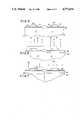
- FIGS. 1-8show in cross section a portion of a silicon wafer in successive stages of its manufacture into CMOS integrated circuit devices in accordance with an illustrative embodiment of the invention.
- FIG. 1shows a monocrystalline silicon wafer in which a large number of integrated circuit devices are formed in parallel for subsequent dicing into discrete chips, each of which includes one or more CMOS integrated circuit devices. Because of the small sizes involved, particularly in the vertical direction, it is not practical to show the figures to scale.
- the substrate 10is shown including along the top or active surface where the devices are to be formed a first well 12 of N-type conductivity adjacent a second well 14 of the opposite or P-type conductivity, for forming a PN junction 15 therebetween. Additionally, at the intersection of the PN junction with the surface, a field oxide layer 18 overlies the surface. At the interface between the field oxide and the silicon substrate, it is usual to include localized more heavily doped N-type and P-type layers, 19 and 20, respectively, to serve as channel stop.
- the wellstypically are several microns deep, for example between three and four microns, and vary widely in lateral extent. Some wells are of a size to accommodate only a single transistor, others of a size to include dozens of transistors. In the illustrative embodiment being described, the wells are each shown of a size to include only a single transistor.
- One techniqueinvolves starting with a silicon substrate on one surface of which is grown an epitaxial layer that is only lightly doped and then doing a first selective implantation of a dopant of one type to form the first well and then, after masking this implanted region, implanting again with a dopant of the opposite type to form the second well.
- each of these wellshas doping levels in the range of between about 10 16 and 10 17 ions per cubic centimeter.
- the channel stops and the field oxidein any known fashion. Generally this involves separate selective implantations to form each of the two channel stops followed by a localized oxidation step.
- boron fluorideis used as the source to implant a relatively light dosage of 10 12 boron ions per square centimeter at an accelerating voltage of about fifty thousand electron volts to form a shallow P-type layer, denoted by the broken line 22 in FIG. 2.
- the channel stops 19, 20 shown in FIG. 1are not being shown in the subsequent FIGS. 2-7, although they remain under the field oxide regions 18 to the end and are shown in FIG. 8.
- the active surfaceis covered with a layer of a suitable masking material, for example, a photoresist, that is patterned photolithographically in the usual fashion to expose selectively the N-well region and this is followed by an N-type implantation, typically a donor, such as phosphorous at a dosage of about 10 12 ions per square centimeter at an accelerating voltage of about seventy-five thousand electron volts.
- a donorsuch as phosphorous at a dosage of about 10 12 ions per square centimeter at an accelerating voltage of about seventy-five thousand electron volts.
- This implantationis used to control the punch through voltage of P-channel transistors to be formed in this well.
- the mask portion 25overlying the P-type well 14. After the implantation, the mask 25 is removed.
- the boron-rich layer 22 and the phosphorous-rich layer 24are not shown since their effects are confined closely to the surface and primarily influence conductivity rather than the conductivity type.
- the gate oxideover the active surface of the substrate in conventional fashion, typically by heating the wafer in an oxidizing atmosphere for a time suitable to form the desired thickness of oxide typically between 150 and 175 Angstroms. This thickness is generally small enough not to impede significantly in any subsequent ion implantations.
- a layer of a material suitable for use as the gate electrodetypically this may either consist of polysilicon doped to be N-type conductive or a composite of an underlying layer of N-doped polysilicon and an overlying layer of a silicide, such as titanium or tantalum silicide, to insure high conductivity to the layer.
- This layeris thereafter suitably patterned to leave separate portions suitable as gate electrodes 26, 28 over the wells. The resultant is shown in FIG. 4 with gate electrodes 26 and 28, overlying the gate oxide layer 30.
- dielectric spacer 32 seen in FIG. 5it is desirable to form dielectric spacer 32 seen in FIG. 5 on each side edge of the gate electrodes to insure isolation from the source and drain electrodes eventually to be provided and also to insure that the source and drain regions subsequently to be formed do not extend below the gate electrodes, which would undesirably increase the gate capacitances.
- the usual techniquecan also be used to form these dielectric spacers.
- a conformed layer of silicon oxidedeposited at low temperature over each electrode of a thickness comparable to the widest width desired of the spacer.
- this silicon oxide layeris etched anisotropically in an etchant that etches vertically much faster than horizontally so that after the layer portion over the top surface of each gate electrode has been removed there remains the edge portions 32 as shown.
- reactive ion etchingRIE
- RIEreactive ion etching
- a layer of masking materialsuch as a photoresist, that is patterned to cover selectively one of the two wells, leaving the other exposed.
- a P-type wellis covered with a layer 35, and N-type well 12 is essentially exposed where covered by the gate electrode 26 and its dielectric spacers 32.
- the gate oxide layer 30is too thin to have any significant masking effect.
- Oneis an implantation of an N-type impurity, such as phosphorous, at a dosage of about 10 13 ions per square centimeter and an accelerating voltage of between one hundred thousand and one hundred and twenty thousand electron volts to form a deep implanted layer of phosphorous.
- the otheris an implantation of boron fluoride at a dosage of about 10 13 boron ions per square centimeter at an accelerating voltage of about fifty thousand electron volts to form a shallower implanted layer of boron that will form the source and drain regions of the P-type channel MOS transistor formed in the N-well.
- the deeper layer of phosphorouswill eventually form in known fashion a halo region underlying the source and drain regions and extending between the source and drain regions at the interface with the channel region underlying the gate electrodes as will be discussed later in connection with FIG. 8.
- the masking layer 35is removed.
- the source and drain regions of the N-channel transistorcan be formed in the P-type well 14. These can be formed in conventional fashion in a manner analogous to that used to form the source and drain regions of the P-channel transistor. This would involve masking the N-type well 12, leaving P-type well 14 exposed and implanting an N-type ion, such as phosphorous or arsenic, to form an implanted layer of such ions on opposite sides of the gate electrode, where not blocked by the gate electrode 28 and its dielectric spacers 32.
- an N-type ionsuch as phosphorous or arsenic
- the preferred embodiment of the inventionuses a differential oxide growth technique.
- This techniquedepends on the known fact that on a silicon substrate a thermal oxide will grow faster, and so thicker for a given exposure, the more doped the substrate.
- the N-type well portion 12will grow a surface oxide thicker where the silicon is exposed than will the surface of P-type well portion 14 where similarly exposed.
- arsenic of a dose of about 10 13 ions per square centimeter implanted at an accelerating voltage of about sixty thousand electron voltswill satisfactorily penetrate the relatively thin oxide layer 42 on the P-type well while being substantially blocked by the thicker oxide layer 40 over the N-type well, as shown by the dashed lines in FIG. 7.
- an implanted layer of arsenicdenoted by the dot-dashline 44 in the substrate on opposite sides of the gate electrode 28, as is shown in FIG. 7.
- the waferis heated to a suitable temperature for activating the implanted ions so that they can serve to affect the conductivity type where they are located.
- the resultant structure in the waferis depicted in FIG. 8.
- the earlier implanted layer for affecting threshold voltages and punch-throughtypically are overcompensated by the later heavier dosages of implanted ions as far as affecting conductivity type in the source and drain regions, but they do influence the properties of the gate electrode-gate oxide interface in the desired fashion.
- the N-type well 12includes the P-channel transistor comprising heavily doped P-type source/drain regions 101 and 102 provided by the boron implantation step shown in FIG. 6. Associated with each of these regions are the halo regions 103, 104 that are less heavily doped P-type because of the compensating effect of the phosphorous implant shown in FIG. 6. Underlying the gate electrode 26 is the channel region that includes a thin P-type surface layer 106 resulting from the first boron implant shown in FIG. 1. Because of this implant and because the gate electrode includes N-type polysilicon at the interface with the gate electrode, the transistor formed in the N-type well is of the type described as a buried channel P-type transistor. The channel region will also include a deeper more heavily doped N-type layer (not shown) produced by the phosphorous implant depicted in FIG. 2 to provide punch-through protection.
- the N-channel transistorcomprising heavily doped N-type source/drain regions 110, 111 produced by the arsenic implant shown in FIG. 7. Associated with these are the less heavily doped N-type halos 114, 115 resulting from the phosphorous implant shown in FIG. 4 before the formation of the spacers on the edges of electrode 28.
Landscapes
- Metal-Oxide And Bipolar Metal-Oxide Semiconductor Integrated Circuits (AREA)
- Insulated Gate Type Field-Effect Transistor (AREA)
Abstract
Description
Claims (5)
Priority Applications (5)
| Application Number | Priority Date | Filing Date | Title |
|---|---|---|---|
| US07/099,144US4771014A (en) | 1987-09-18 | 1987-09-18 | Process for manufacturing LDD CMOS devices |
| EP88402217AEP0308295B1 (en) | 1987-09-18 | 1988-09-02 | Process for manufacturing cmos devices |
| DE88402217TDE3881799T2 (en) | 1987-09-18 | 1988-09-02 | Process for the production of CMOS components. |
| KR1019880011830AKR0130549B1 (en) | 1987-09-18 | 1988-09-13 | Process for manufacturing ldd cmos device |
| JP63234681AJP2663402B2 (en) | 1987-09-18 | 1988-09-19 | Method for manufacturing CMOS integrated circuit device |
Applications Claiming Priority (1)
| Application Number | Priority Date | Filing Date | Title |
|---|---|---|---|
| US07/099,144US4771014A (en) | 1987-09-18 | 1987-09-18 | Process for manufacturing LDD CMOS devices |
Publications (1)
| Publication Number | Publication Date |
|---|---|
| US4771014Atrue US4771014A (en) | 1988-09-13 |
Family
ID=22273059
Family Applications (1)
| Application Number | Title | Priority Date | Filing Date |
|---|---|---|---|
| US07/099,144Expired - LifetimeUS4771014A (en) | 1987-09-18 | 1987-09-18 | Process for manufacturing LDD CMOS devices |
Country Status (5)
| Country | Link |
|---|---|
| US (1) | US4771014A (en) |
| EP (1) | EP0308295B1 (en) |
| JP (1) | JP2663402B2 (en) |
| KR (1) | KR0130549B1 (en) |
| DE (1) | DE3881799T2 (en) |
Cited By (31)
| Publication number | Priority date | Publication date | Assignee | Title |
|---|---|---|---|---|
| US4876213A (en)* | 1988-10-31 | 1989-10-24 | Motorola, Inc. | Salicided source/drain structure |
| US4889825A (en)* | 1986-03-04 | 1989-12-26 | Motorola, Inc. | High/low doping profile for twin well process |
| US4908327A (en)* | 1988-05-02 | 1990-03-13 | Texas Instruments, Incorporated | Counter-doped transistor |
| US4949136A (en)* | 1988-06-09 | 1990-08-14 | University Of Connecticut | Submicron lightly doped field effect transistors |
| US4997782A (en)* | 1988-08-04 | 1991-03-05 | Sgs-Thomson Microelectronics S.R.L. | Fabrication of CMOS integrated devices with reduced gate length and lightly doped drain |
| US5015595A (en)* | 1988-09-09 | 1991-05-14 | Advanced Micro Devices, Inc. | Method of making a high performance MOS device having both P- and N-LDD regions using single photoresist mask |
| US5021354A (en)* | 1989-12-04 | 1991-06-04 | Motorola, Inc. | Process for manufacturing a semiconductor device |
| US5030582A (en)* | 1988-10-14 | 1991-07-09 | Matsushita Electric Industrial Co., Ltd. | Method of fabricating a CMOS semiconductor device |
| EP0462416A3 (en)* | 1990-05-24 | 1992-03-11 | Micron Technology, Inc. | Process for n-well and p-well creation on a silicon substrate using a blanket p-well implant and no n-well steam oxidation step |
| US5097310A (en)* | 1988-09-29 | 1992-03-17 | Mitsubishi Denki Kabushiki Kaisha | Complementary semiconductor device having improved device isolating region |
| US5262664A (en)* | 1990-06-30 | 1993-11-16 | Goldstar Electron Co., Ltd. | Process for formation of LDD transistor, and structure thereof |
| US5273914A (en)* | 1988-10-14 | 1993-12-28 | Matsushita Electric Industrial Co., Ltd. | Method of fabricating a CMOS semiconductor devices |
| US5328862A (en)* | 1992-06-12 | 1994-07-12 | Goldstar Electron Co., Ltd. | Method of making metal oxide semiconductor field effect transistor |
| US5384279A (en)* | 1988-09-09 | 1995-01-24 | U.S. Philips Corporation | Method of manufacturing a semiconductor device comprising a silicon body in which semiconductor regions are formed by ion implantations |
| US5399513A (en)* | 1989-06-27 | 1995-03-21 | National Semiconductor Corporation | Salicide compatible CMOS process with a differential oxide implant mask |
| US5405791A (en)* | 1994-10-04 | 1995-04-11 | Micron Semiconductor, Inc. | Process for fabricating ULSI CMOS circuits using a single polysilicon gate layer and disposable spacers |
| US5413945A (en)* | 1994-08-12 | 1995-05-09 | United Micro Electronics Corporation | Blanket N-LDD implantation for sub-micron MOS device manufacturing |
| WO1995027305A1 (en)* | 1994-03-31 | 1995-10-12 | Vlsi Technology, Inc. | Mosfet with gate-penetrating halo implant |
| WO1996004679A1 (en)* | 1994-08-01 | 1996-02-15 | National Semiconductor Corporation | Counter-implantation method of manufacturing a semiconductor device with self-aligned anti-punchthrough pockets |
| US5534449A (en)* | 1995-07-17 | 1996-07-09 | Micron Technology, Inc. | Methods of forming complementary metal oxide semiconductor (CMOS) integrated circuitry |
| US5595918A (en)* | 1995-03-23 | 1997-01-21 | International Rectifier Corporation | Process for manufacture of P channel MOS-gated device |
| US5654213A (en)* | 1995-10-03 | 1997-08-05 | Integrated Device Technology, Inc. | Method for fabricating a CMOS device |
| US5686324A (en)* | 1996-03-28 | 1997-11-11 | Mosel Vitelic, Inc. | Process for forming LDD CMOS using large-tilt-angle ion implantation |
| US5716861A (en)* | 1991-06-26 | 1998-02-10 | Texas Instruments Incorporated | Insulated-gate field-effect transistor structure and method |
| US5837587A (en)* | 1991-09-30 | 1998-11-17 | Sgs-Thomson Microelectronics, Inc. | Method of forming an integrated circuit device |
| US5861334A (en)* | 1995-08-07 | 1999-01-19 | Hyundai Electronics Industries Co., | Method for fabricating semiconductor device having a buried channel |
| US6004854A (en)* | 1995-07-17 | 1999-12-21 | Micron Technology, Inc. | Method of forming CMOS integrated circuitry |
| US6025232A (en)* | 1997-11-12 | 2000-02-15 | Micron Technology, Inc. | Methods of forming field effect transistors and related field effect transistor constructions |
| US6171914B1 (en) | 1999-06-14 | 2001-01-09 | Taiwan Semiconductor Manufacturing Company | Synchronized implant process to simplify NLDD/PLDD stage and N+/P+stage into one implant |
| US6252278B1 (en)* | 1998-05-18 | 2001-06-26 | Monolithic Power Systems, Inc. | Self-aligned lateral DMOS with spacer drift region |
| US20030209847A1 (en)* | 2002-05-10 | 2003-11-13 | Allison Claudia Leigh | Handling device comprising multiple immobilization segments |
Families Citing this family (1)
| Publication number | Priority date | Publication date | Assignee | Title |
|---|---|---|---|---|
| US5234167A (en)* | 1989-11-16 | 1993-08-10 | Afa Products, Inc. | One-piece foamer nozzle |
Citations (6)
| Publication number | Priority date | Publication date | Assignee | Title |
|---|---|---|---|---|
| US4530150A (en)* | 1982-09-20 | 1985-07-23 | Fujitsu Limited | Method of forming conductive channel extensions to active device regions in CMOS device |
| US4562638A (en)* | 1983-11-09 | 1986-01-07 | Siemens Aktiengesellschaft | Method for the simultaneous manufacture of fast short channel and voltage-stable MOS transistors in VLSI circuits |
| US4590663A (en)* | 1982-02-01 | 1986-05-27 | Texas Instruments Incorporated | High voltage CMOS technology with N-channel source/drain extensions |
| US4599789A (en)* | 1984-06-15 | 1986-07-15 | Harris Corporation | Process of making twin well VLSI CMOS |
| US4637124A (en)* | 1984-03-16 | 1987-01-20 | Hitachi, Ltd. | Process for fabricating semiconductor integrated circuit device |
| US4642878A (en)* | 1984-08-28 | 1987-02-17 | Kabushiki Kaisha Toshiba | Method of making MOS device by sequentially depositing an oxidizable layer and a masking second layer over gated device regions |
Family Cites Families (5)
| Publication number | Priority date | Publication date | Assignee | Title |
|---|---|---|---|---|
| JPS6029229B2 (en)* | 1976-12-21 | 1985-07-09 | 日本電気株式会社 | Semiconductor integrated circuit device |
| JPS5923562A (en)* | 1982-07-30 | 1984-02-07 | Hitachi Ltd | Insulated gate field effect semiconductor device and manufacturing method thereof |
| JPS5932163A (en)* | 1982-08-18 | 1984-02-21 | Nec Corp | CMOS integrated circuit |
| US4480375A (en)* | 1982-12-09 | 1984-11-06 | International Business Machines Corporation | Simple process for making complementary transistors |
| US4577391A (en)* | 1984-07-27 | 1986-03-25 | Monolithic Memories, Inc. | Method of manufacturing CMOS devices |
- 1987
- 1987-09-18USUS07/099,144patent/US4771014A/ennot_activeExpired - Lifetime
- 1988
- 1988-09-02EPEP88402217Apatent/EP0308295B1/ennot_activeExpired - Lifetime
- 1988-09-02DEDE88402217Tpatent/DE3881799T2/ennot_activeExpired - Fee Related
- 1988-09-13KRKR1019880011830Apatent/KR0130549B1/ennot_activeExpired - Fee Related
- 1988-09-19JPJP63234681Apatent/JP2663402B2/ennot_activeExpired - Fee Related
Patent Citations (6)
| Publication number | Priority date | Publication date | Assignee | Title |
|---|---|---|---|---|
| US4590663A (en)* | 1982-02-01 | 1986-05-27 | Texas Instruments Incorporated | High voltage CMOS technology with N-channel source/drain extensions |
| US4530150A (en)* | 1982-09-20 | 1985-07-23 | Fujitsu Limited | Method of forming conductive channel extensions to active device regions in CMOS device |
| US4562638A (en)* | 1983-11-09 | 1986-01-07 | Siemens Aktiengesellschaft | Method for the simultaneous manufacture of fast short channel and voltage-stable MOS transistors in VLSI circuits |
| US4637124A (en)* | 1984-03-16 | 1987-01-20 | Hitachi, Ltd. | Process for fabricating semiconductor integrated circuit device |
| US4599789A (en)* | 1984-06-15 | 1986-07-15 | Harris Corporation | Process of making twin well VLSI CMOS |
| US4642878A (en)* | 1984-08-28 | 1987-02-17 | Kabushiki Kaisha Toshiba | Method of making MOS device by sequentially depositing an oxidizable layer and a masking second layer over gated device regions |
Non-Patent Citations (2)
| Title |
|---|
| Ogura et al., "A Half-Micron MOSFET Using Double Implanted LDD", IEDM 1982, pp. 718-721. |
| Ogura et al., A Half Micron MOSFET Using Double Implanted LDD , IEDM 1982, pp. 718 721.* |
Cited By (52)
| Publication number | Priority date | Publication date | Assignee | Title |
|---|---|---|---|---|
| US4889825A (en)* | 1986-03-04 | 1989-12-26 | Motorola, Inc. | High/low doping profile for twin well process |
| US4908327A (en)* | 1988-05-02 | 1990-03-13 | Texas Instruments, Incorporated | Counter-doped transistor |
| US4949136A (en)* | 1988-06-09 | 1990-08-14 | University Of Connecticut | Submicron lightly doped field effect transistors |
| US4997782A (en)* | 1988-08-04 | 1991-03-05 | Sgs-Thomson Microelectronics S.R.L. | Fabrication of CMOS integrated devices with reduced gate length and lightly doped drain |
| US5015595A (en)* | 1988-09-09 | 1991-05-14 | Advanced Micro Devices, Inc. | Method of making a high performance MOS device having both P- and N-LDD regions using single photoresist mask |
| US5384279A (en)* | 1988-09-09 | 1995-01-24 | U.S. Philips Corporation | Method of manufacturing a semiconductor device comprising a silicon body in which semiconductor regions are formed by ion implantations |
| US5097310A (en)* | 1988-09-29 | 1992-03-17 | Mitsubishi Denki Kabushiki Kaisha | Complementary semiconductor device having improved device isolating region |
| US5030582A (en)* | 1988-10-14 | 1991-07-09 | Matsushita Electric Industrial Co., Ltd. | Method of fabricating a CMOS semiconductor device |
| US5273914A (en)* | 1988-10-14 | 1993-12-28 | Matsushita Electric Industrial Co., Ltd. | Method of fabricating a CMOS semiconductor devices |
| US4876213A (en)* | 1988-10-31 | 1989-10-24 | Motorola, Inc. | Salicided source/drain structure |
| US5399513A (en)* | 1989-06-27 | 1995-03-21 | National Semiconductor Corporation | Salicide compatible CMOS process with a differential oxide implant mask |
| US5021354A (en)* | 1989-12-04 | 1991-06-04 | Motorola, Inc. | Process for manufacturing a semiconductor device |
| EP0462416A3 (en)* | 1990-05-24 | 1992-03-11 | Micron Technology, Inc. | Process for n-well and p-well creation on a silicon substrate using a blanket p-well implant and no n-well steam oxidation step |
| US5262664A (en)* | 1990-06-30 | 1993-11-16 | Goldstar Electron Co., Ltd. | Process for formation of LDD transistor, and structure thereof |
| US5716861A (en)* | 1991-06-26 | 1998-02-10 | Texas Instruments Incorporated | Insulated-gate field-effect transistor structure and method |
| US5949105A (en)* | 1991-06-26 | 1999-09-07 | Texas Instruments Incorporated | Insulated-gate field-effect transistor structure and method |
| US6027979A (en)* | 1991-09-30 | 2000-02-22 | Stmicroelectronics, Inc. | Method of forming an integrated circuit device |
| US5837587A (en)* | 1991-09-30 | 1998-11-17 | Sgs-Thomson Microelectronics, Inc. | Method of forming an integrated circuit device |
| US5894158A (en)* | 1991-09-30 | 1999-04-13 | Stmicroelectronics, Inc. | Having halo regions integrated circuit device structure |
| US5328862A (en)* | 1992-06-12 | 1994-07-12 | Goldstar Electron Co., Ltd. | Method of making metal oxide semiconductor field effect transistor |
| WO1995027305A1 (en)* | 1994-03-31 | 1995-10-12 | Vlsi Technology, Inc. | Mosfet with gate-penetrating halo implant |
| WO1996004679A1 (en)* | 1994-08-01 | 1996-02-15 | National Semiconductor Corporation | Counter-implantation method of manufacturing a semiconductor device with self-aligned anti-punchthrough pockets |
| US5413945A (en)* | 1994-08-12 | 1995-05-09 | United Micro Electronics Corporation | Blanket N-LDD implantation for sub-micron MOS device manufacturing |
| US5405791A (en)* | 1994-10-04 | 1995-04-11 | Micron Semiconductor, Inc. | Process for fabricating ULSI CMOS circuits using a single polysilicon gate layer and disposable spacers |
| US5595918A (en)* | 1995-03-23 | 1997-01-21 | International Rectifier Corporation | Process for manufacture of P channel MOS-gated device |
| US5776806A (en)* | 1995-07-17 | 1998-07-07 | Micron Technology, Inc. | Method of forming CMOS integrated circuitry having halo regions |
| US6261888B1 (en) | 1995-07-17 | 2001-07-17 | Micron Technology, Inc. | Method of forming CMOS integrated circuitry |
| US5747855A (en)* | 1995-07-17 | 1998-05-05 | Micron Technology, Inc. | CMOS integrated circuitry with Halo and LDD regions |
| US5683927A (en)* | 1995-07-17 | 1997-11-04 | Micron Technology, Inc. | Method of forming CMOS integrated circuitry |
| US6004854A (en)* | 1995-07-17 | 1999-12-21 | Micron Technology, Inc. | Method of forming CMOS integrated circuitry |
| US5534449A (en)* | 1995-07-17 | 1996-07-09 | Micron Technology, Inc. | Methods of forming complementary metal oxide semiconductor (CMOS) integrated circuitry |
| US6074924A (en)* | 1995-07-17 | 2000-06-13 | Micron Technology, Inc. | Method of forming CMOS integrated circuitry |
| US6124616A (en)* | 1995-07-17 | 2000-09-26 | Micron Technology, Inc. | Integrated circuitry comprising halo regions and LDD regions |
| US6358787B2 (en) | 1995-07-17 | 2002-03-19 | Micron Technology, Inc. | Method of forming CMOS integrated circuitry |
| US5861334A (en)* | 1995-08-07 | 1999-01-19 | Hyundai Electronics Industries Co., | Method for fabricating semiconductor device having a buried channel |
| US5654213A (en)* | 1995-10-03 | 1997-08-05 | Integrated Device Technology, Inc. | Method for fabricating a CMOS device |
| US5750424A (en)* | 1995-10-03 | 1998-05-12 | Integrated Device Technology, Inc. | Method for fabricating a CMOS device |
| US5686324A (en)* | 1996-03-28 | 1997-11-11 | Mosel Vitelic, Inc. | Process for forming LDD CMOS using large-tilt-angle ion implantation |
| US6400002B1 (en) | 1997-11-12 | 2002-06-04 | Micron Technology, Inc. | Methods of forming field effect transistors and related field effect transistor constructions |
| US6406957B1 (en) | 1997-11-12 | 2002-06-18 | Micron Technology, Inc. | Methods of forming field effect transistors and related field effect transistor constructions |
| US6335246B1 (en) | 1997-11-12 | 2002-01-01 | Micron Technology, Inc. | Methods of forming field effect transistors and related field effect transistor constructions |
| US6335234B2 (en) | 1997-11-12 | 2002-01-01 | Micron Technology, Inc. | Methods of forming field effect transistors and related field effect transistor constructions |
| US6344382B1 (en) | 1997-11-12 | 2002-02-05 | Micron Technology, Inc. | Methods of forming field effect transistors and related field effect transistor constructions |
| US6673663B2 (en) | 1997-11-12 | 2004-01-06 | Micron Technology, Inc. | Methods of forming field effect transistors and related field effect transistor constructions |
| US6025232A (en)* | 1997-11-12 | 2000-02-15 | Micron Technology, Inc. | Methods of forming field effect transistors and related field effect transistor constructions |
| US6482691B2 (en) | 1997-11-12 | 2002-11-19 | Micron Technology, Inc. | Seismic imaging using omni-azimuth seismic energy sources and directional sensing |
| US6413823B1 (en) | 1997-11-12 | 2002-07-02 | Micron Technology, Inc. | Methods of forming field effect transistors |
| US6472260B2 (en) | 1997-11-12 | 2002-10-29 | Micron Technology, Inc. | Methods of forming field effect transistors and related field effect transistor constructions |
| US6475852B2 (en) | 1997-11-12 | 2002-11-05 | Micron Technology, Inc. | Method of forming field effect transistors and related field effect transistor constructions |
| US6252278B1 (en)* | 1998-05-18 | 2001-06-26 | Monolithic Power Systems, Inc. | Self-aligned lateral DMOS with spacer drift region |
| US6171914B1 (en) | 1999-06-14 | 2001-01-09 | Taiwan Semiconductor Manufacturing Company | Synchronized implant process to simplify NLDD/PLDD stage and N+/P+stage into one implant |
| US20030209847A1 (en)* | 2002-05-10 | 2003-11-13 | Allison Claudia Leigh | Handling device comprising multiple immobilization segments |
Also Published As
| Publication number | Publication date |
|---|---|
| KR890005894A (en) | 1989-05-17 |
| KR0130549B1 (en) | 1998-04-06 |
| JP2663402B2 (en) | 1997-10-15 |
| DE3881799D1 (en) | 1993-07-22 |
| DE3881799T2 (en) | 1993-10-07 |
| EP0308295B1 (en) | 1993-06-16 |
| JPH01101662A (en) | 1989-04-19 |
| EP0308295A1 (en) | 1989-03-22 |
Similar Documents
| Publication | Publication Date | Title |
|---|---|---|
| US4771014A (en) | Process for manufacturing LDD CMOS devices | |
| US5359219A (en) | Silicon on insulator device comprising improved substrate doping | |
| US4717683A (en) | CMOS process | |
| US5266510A (en) | High performance sub-micron p-channel transistor with germanium implant | |
| US4554726A (en) | CMOS Integrated circuit technology utilizing dual implantation of slow and fast diffusing donor ions to form the n-well | |
| KR930010121B1 (en) | Process for forming high and low voltage CMOS transistors on a single integrated circuit chip | |
| US4503601A (en) | Oxide trench structure for polysilicon gates and interconnects | |
| US4764482A (en) | Method of fabricating an integrated circuit containing bipolar and MOS transistors | |
| JP3077630B2 (en) | Semiconductor device and manufacturing method thereof | |
| US4345366A (en) | Self-aligned all-n+ polysilicon CMOS process | |
| US4697332A (en) | Method of making tri-well CMOS by self-aligned process | |
| US4902639A (en) | Process for making BiCMOS integrated circuit having a shallow trench bipolar transistor with vertical base contacts | |
| US5821147A (en) | Integrated circuit fabrication | |
| US5047812A (en) | Insulated gate field effect device | |
| US4786955A (en) | Semiconductor device with source and drain depth extenders and a method of making the same | |
| JPH07201974A (en) | Method for manufacturing semiconductor device | |
| US6261885B1 (en) | Method for forming integrated circuit gate conductors from dual layers of polysilicon | |
| US5348896A (en) | Method for fabricating a BiCMOS device | |
| KR100227872B1 (en) | Semiconductor device and process for making the same | |
| US4481705A (en) | Process for doping field isolation regions in CMOS integrated circuits | |
| GB2036431A (en) | Double diffused transistor structure | |
| KR100214297B1 (en) | Manufacturing Method of Semiconductor Device | |
| KR950002200B1 (en) | MOSFET structure and manufacturing method | |
| WO1990005993A1 (en) | High performance sub-micron p-channel transistor with germanium implant | |
| JPH07115195A (en) | Mos transistor and its manufacture |
Legal Events
| Date | Code | Title | Description |
|---|---|---|---|
| AS | Assignment | Owner name:THOMSON COMPONENTS-MOSTEK CORPORATION, 1310 ELECTR Free format text:ASSIGNMENT OF ASSIGNORS INTEREST.;ASSIGNORS:LIOU, FU-TAI;HAN, YU-PIN;BRYANT, FRANK R.;REEL/FRAME:004779/0755 Effective date:19870910 Owner name:THOMSON COMPONENTS-MOSTEK CORPORATION,TEXAS Free format text:ASSIGNMENT OF ASSIGNORS INTEREST;ASSIGNORS:LIOU, FU-TAI;HAN, YU-PIN;BRYANT, FRANK R.;REEL/FRAME:004779/0755 Effective date:19870910 | |
| STCF | Information on status: patent grant | Free format text:PATENTED CASE | |
| AS | Assignment | Owner name:SGS-THOMSON MICROELECTRONICS, INC. Free format text:CHANGE OF NAME;ASSIGNOR:THOMSON COMPONENTS-MOSTEK CORPORATION;REEL/FRAME:005270/0714 Effective date:19871023 Owner name:SGS-THOMSON MICROELECTRONICS, INC. Free format text:MERGER;ASSIGNORS:SGS SEMICONDUCTOR CORPORATION, A CORP. OF DE;THOMSON HOLDINGS (DELAWARE) INC., A CORP. OF DE;SGS-THOMSON MICROELECTRONICS, INC. A CORP. OF DE (MERGED INTO);REEL/FRAME:005270/0725 Effective date:19871224 | |
| FEPP | Fee payment procedure | Free format text:PAYOR NUMBER ASSIGNED (ORIGINAL EVENT CODE: ASPN); ENTITY STATUS OF PATENT OWNER: LARGE ENTITY | |
| FPAY | Fee payment | Year of fee payment:4 | |
| FPAY | Fee payment | Year of fee payment:8 | |
| FEPP | Fee payment procedure | Free format text:PAYER NUMBER DE-ASSIGNED (ORIGINAL EVENT CODE: RMPN); ENTITY STATUS OF PATENT OWNER: LARGE ENTITY Free format text:PAYOR NUMBER ASSIGNED (ORIGINAL EVENT CODE: ASPN); ENTITY STATUS OF PATENT OWNER: LARGE ENTITY | |
| FPAY | Fee payment | Year of fee payment:12 |