US4768961A - Jackfield with front removable jack modules having lamp assemblies - Google Patents
Jackfield with front removable jack modules having lamp assembliesDownload PDFInfo
- Publication number
- US4768961A US4768961AUS07/106,291US10629187AUS4768961AUS 4768961 AUS4768961 AUS 4768961AUS 10629187 AUS10629187 AUS 10629187AUS 4768961 AUS4768961 AUS 4768961A
- Authority
- US
- United States
- Prior art keywords
- jack
- printed circuit
- circuit board
- lamp
- housing
- Prior art date
- Legal status (The legal status is an assumption and is not a legal conclusion. Google has not performed a legal analysis and makes no representation as to the accuracy of the status listed.)
- Expired - Fee Related
Links
- 230000000712assemblyEffects0.000titleabstractdescription6
- 238000000429assemblyMethods0.000titleabstractdescription6
- 239000004020conductorSubstances0.000claimsabstractdescription64
- 238000010618wire wrapMethods0.000claimsabstractdescription19
- 238000003780insertionMethods0.000claimsdescription8
- 230000037431insertionEffects0.000claimsdescription8
- 239000002184metalSubstances0.000claimsdescription7
- 230000004044responseEffects0.000claimsdescription2
- 210000003739neckAnatomy0.000description19
- 238000005192partitionMethods0.000description7
- 235000012431wafersNutrition0.000description6
- 239000012212insulatorSubstances0.000description4
- 230000008901benefitEffects0.000description3
- 239000004033plasticSubstances0.000description3
- 238000012360testing methodMethods0.000description3
- 210000005069earsAnatomy0.000description2
- 239000004593EpoxySubstances0.000description1
- 239000004677NylonSubstances0.000description1
- 230000004075alterationEffects0.000description1
- 230000008859changeEffects0.000description1
- 238000004891communicationMethods0.000description1
- 238000010276constructionMethods0.000description1
- 230000000881depressing effectEffects0.000description1
- 239000011521glassSubstances0.000description1
- 238000004519manufacturing processMethods0.000description1
- 238000000034methodMethods0.000description1
- 238000012986modificationMethods0.000description1
- 230000004048modificationEffects0.000description1
- 239000002991molded plasticSubstances0.000description1
- 238000012544monitoring processMethods0.000description1
- 229920001778nylonPolymers0.000description1
- 230000008569processEffects0.000description1
- 238000012545processingMethods0.000description1
- 230000008439repair processEffects0.000description1
- 230000000452restraining effectEffects0.000description1
Images


Classifications
- H—ELECTRICITY
- H01—ELECTRIC ELEMENTS
- H01R—ELECTRICALLY-CONDUCTIVE CONNECTIONS; STRUCTURAL ASSOCIATIONS OF A PLURALITY OF MUTUALLY-INSULATED ELECTRICAL CONNECTING ELEMENTS; COUPLING DEVICES; CURRENT COLLECTORS
- H01R24/00—Two-part coupling devices, or either of their cooperating parts, characterised by their overall structure
- H01R24/58—Contacts spaced along longitudinal axis of engagement
- H—ELECTRICITY
- H01—ELECTRIC ELEMENTS
- H01R—ELECTRICALLY-CONDUCTIVE CONNECTIONS; STRUCTURAL ASSOCIATIONS OF A PLURALITY OF MUTUALLY-INSULATED ELECTRICAL CONNECTING ELEMENTS; COUPLING DEVICES; CURRENT COLLECTORS
- H01R13/00—Details of coupling devices of the kinds covered by groups H01R12/70 or H01R24/00 - H01R33/00
- H01R13/46—Bases; Cases
- H01R13/516—Means for holding or embracing insulating body, e.g. casing, hoods
- H01R13/518—Means for holding or embracing insulating body, e.g. casing, hoods for holding or embracing several coupling parts, e.g. frames
- H—ELECTRICITY
- H01—ELECTRIC ELEMENTS
- H01R—ELECTRICALLY-CONDUCTIVE CONNECTIONS; STRUCTURAL ASSOCIATIONS OF A PLURALITY OF MUTUALLY-INSULATED ELECTRICAL CONNECTING ELEMENTS; COUPLING DEVICES; CURRENT COLLECTORS
- H01R13/00—Details of coupling devices of the kinds covered by groups H01R12/70 or H01R24/00 - H01R33/00
- H01R13/66—Structural association with built-in electrical component
- H01R13/717—Structural association with built-in electrical component with built-in light source
- H01R13/7177—Structural association with built-in electrical component with built-in light source filament or neon bulb
- H—ELECTRICITY
- H01—ELECTRIC ELEMENTS
- H01R—ELECTRICALLY-CONDUCTIVE CONNECTIONS; STRUCTURAL ASSOCIATIONS OF A PLURALITY OF MUTUALLY-INSULATED ELECTRICAL CONNECTING ELEMENTS; COUPLING DEVICES; CURRENT COLLECTORS
- H01R2103/00—Two poles
- H—ELECTRICITY
- H05—ELECTRIC TECHNIQUES NOT OTHERWISE PROVIDED FOR
- H05K—PRINTED CIRCUITS; CASINGS OR CONSTRUCTIONAL DETAILS OF ELECTRIC APPARATUS; MANUFACTURE OF ASSEMBLAGES OF ELECTRICAL COMPONENTS
- H05K1/00—Printed circuits
- H05K1/18—Printed circuits structurally associated with non-printed electric components
Definitions
- the field of the inventiongenerally relates to electrical jacks, and more particularly to a jack module including a printed circuit board and lamp assembly which is removable from the front of a jackfield housing.
- Electrical jacksare commonly used for digital or voice frequency interconnections in applications such as, for example, telephone central offices, testing and patch panels, computer and data processing equipment, multiplex gear, and commercial and industrial patching and control applications.
- a plurality of jackseach of which may have, for example, three forward facing jack sleeves are arranged side-by-side in a housing or enclosure that mounts in a rack.
- input and output circuitsare connected to the back, and the jack sleeves are available on the front for inserting patch cord plugs to interconnect, monitor, or test circuits.
- each jack moduleincludes a printed circuit board having a front right-angle connector, a tri-jack assembly having pins inserted into the connector, and a forward extending lamp housing connected to the printed circuit board above the connector.
- the tri-jacksare inserted and removed from the front of the jackfield housing, while the printed circuit boards are removed from the rear.
- bus stripswere run laterally in the jackfield housing between the connectors and the tri-jacks, and the strips had perpendicular pins which inserted into connector terminals.
- this jackfieldhad a drawback because the printed circuit boards could not be removed from the front. Among other reasons, the bus strips running laterally in front of the printed circuit boards prevented their front removal. Further, if the printed circuit boards are removed from the rear such as for service or to change the configuration, it is difficult to align the bus pins into the printed circuit board connector.
- a front removable jack moduleincluding a lamp and a printed circuit board having leads interconnecting the lamp to rear conductor pads on the printed circuit board, which conductor pads automatically align in sliding engagement with laterally extending busses in the jackfield housing.
- the busseshave contact springs which are readily engageable and disengageable and in self-alignment with the conductor pads that are located at different vertical levels on the printed circuit board.
- a jack moduleadapted for front insertion and removal from guide slots in a jackfield housing, comprising a printed circuit board having top and bottom edges insertable for longitudinal sliding engagement in the slots, a lamp having a lamp housing connected to and extending forwardly from the printed circuit board, a jack connected to and extending forwardly from the printed circuit board, the jack having terminals electrically connected to the printed circuit board, and the printed circuit board having at least one rear conductor pad adapted for sliding removable engagement with contact spring terminals at the back of the jackfield housing wherein the jack module can be inserted from the front of the jackfield housing in one of the guide slots with the conductor pad electrically engaging the contact spring terminal, the printed circuit board having a conductor lead for interconnecting the conductor pad to the lamp.
- the printed circuit boardhave at least a second rear conductor pad adapted for sliding removable engagement with a second contact spring terminal, the module further comprising a circuit through the jack interconnecting the second conductor pad with the lamp. Also, it is preferable that the circuit from the second conductor pad through the jack to the lamp be activated by insertion of a plug into the jack. It is also preferable that the contact spring and the second contact spring terminals be connected to respective busses that provide a voltage and ground to the lamp for lighting the lamp in response to the plug being inserted into the jack.
- the printed circuit boardcomprise a plurality of wire wrapped lugs extending from the rear and a plurality of conductor leads for interconnecting the lugs to the jack. Accordingly, to remove a module from the front, the wire wraps are removed from the wire wrapped lugs, and the module is pulled forward such that the contact spring terminals slidably disengage the conductor pads.
- a jackfieldcomprising a jackfield housing having a plurality of longitudinal slots each having at least two vertical levels of contact spring terminal connectors aligned therewith, the contact spring terminal connectors on one of the levels being interconnected to a voltage bus, the contact spring terminal connectors on the other one of the levels being interconnected to a ground bus, a plurality of jack modules slidably engaged in the longitudinal slots, each of the modules comprising a printed circuit board having top and bottom edges slidably engaged in the slots of the housing, a lamp having a lamp housing connected to and extending forwardly from the printed circuit board, a jack connected to and extending forwardly from the printed circuit board underneath the lamp housing, the jack having a plurality of forward facing jack sleeves, the jack having a circuit activated by insertion of a plug in one of the jack sleeves, the jack being electrically interconnected to the conductor leads of the printed circuit board, and the printed circuit board having at least two rear conductor pads vertically aligned for
- the jackfieldfurther comprise metal shields positioned between adjacent ones of the slots, the metal shields comprising means for preventing the removal of the shields toward the front of the housing. It is also preferable that the jackfield housing further comprise means for restraining forward motion of the modules when only the jacks are to be removed.
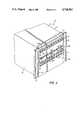
- FIG. 1is a front perspective view of a jackfield
- FIG. 2is an exploded view of a jack module with associated guide apparatus
- FIG. 3is a side view of a jack module mounted in the jackfield
- FIG. 4is an exploded view of the lamp assembly
- FIG. 5is a front sectioned view of a tri-jack
- FIG. 6is a side sectioned view of the bus housing
- FIG. 7is an exploded view of a bus projection and a portion of a bus housing slot
- FIG. 8is a front view of a jackfield
- FIG. 9is a view taken along line 9--9 of FIG. 8.
- FIG. 1shows a front perspective view of electrical jackfield assembly 10 which includes an enclosure or housing 12 and a plurality of vertically elongated modules 14 that are backwardly extending and mounted side-by-side.
- Housing 12is an electromagnetic shielded casing and includes top plate 16, side plates 18, top and bottom rear plates 20 and 22 (FIG. 3), bottom plate 24 (FIG. 3), and top and bottom front plates or panels 26 and 28.
- jackfield assembly 10is mounted in a standard 23-inch rack (not shown) and mounting brackets 30 are provided for this purpose.
- Top and bottom front panels 26 and 28, which will be described in more detail later herein,are connected to the front using screws 32 or other suitable fasteners.
- a standard jackfield assembly 10may consist of 56 side-by-side mounted modules, although other numbers could be used in various configurations.
- Each module 14here has three vertically aligned plug receiving apertures 34a-c or bores, and thus the modules 14 are commonly referred to as tri-jack modules.
- bore 34ais used to monitor the module 14
- bore 34bis used to patch a circuit out of module 14
- bore 34cis used to patch a circuit into module 14.
- Each plug receiving bore 34a-cis surrounded by a cylindrical jack sleeve 36a-c that has a collar 38.
- Each module 14has a lamp assembly 40 with a lamp 42 that protrudes through an elongated lateral window 44 in the top front panel 26.
- Tri-jack moduleincludes printed circuit board 48, a tri-jack assembly 50, a lamp assembly 40, a bottom guide housing 54 for tri-jack assembly 50, and a right-angle connector 56.
- Printed circuit board 48is of conventional construction such as a multi-layer epoxy glass board having a plurality of conductor leads 58 which are deposited in a predetermined pattern on both sides of printed circuit board 48.
- FIG. 2only the conductor leads 58 on one side of printed circuit board 48 are shown, and it is well known and conventional to interconnect conductor leads 58 from the opposite side at terminals such as right-angle connector 56 and at conductive eyelets 60.
- the function of printed circuit board 48is to interconnect wire wrap lugs or pins 62 and 64 through right-angle connector 56 to corresponding terminal pins 66 of tri-jack assembly 50. Further, as will be described in detail later herein, printed circuit board 48 interconnects conductor pads 68a-c to corresponding terminals of lamp assembly 40 and right-angle connector 56.
- printed circuit board 48has top and bottom forwardly projecting posts or necks 70 and 72, respectively, which define a notch 74 therebetween. Also, printed circuit board 48 has top and bottom rearward projections 76 and 78, respectively, which define a notch 80 therebetween. As can be seen best in FIG. 2, top rearward projection 76 on which wire wrap lugs 62 are mounted extends much further than bottom rearward projection 78 on which wire wrap lugs 64 are mounted. Conductor pads 68a-c are positioned inwardly from notch 80.
- lamp assembly 40is connected to top forwardly projecting neck 70 of printed circuit board 48.
- FIG. 4there is shown an exploded perspective view of lamp assembly 40 from the opposite side of that shown in FIG. 2.
- Lamp assembly 40includes lamp housing 82, lamp housing retainer 84, conductor strips 86a and b, and a lamp 42.
- pins 88 of two conductor strips 86a and bare inserted through eyelets (not shown) in neck 70 and soldered in place so that conductor strips 86a and b are parallel and extend horizontally forward.
- lamp housing retainer 84 or center lamp postis inserted between conductor strips 86a and b.
- Lamp housing retainer 84is a molded plastic part and has two positioning pins 90 extending laterally from a flat side 92 that seats up against the neck 70 of printed circuit board 48. Retainer positioning pins 90 insert through small holes 94 in neck 70 thereby accurately locating lamp housing retainer 84 and preventing it from moving in a longitudinal or vertical direction.
- the front 102 of lamp housing retainer 84is pointed, and is contacted on top and bottom by contact terminals 104 of conductor strips 86a and b which are spring tensioned against the top and bottom of retainer front 102.
- Lamp housing 82is a plastic molded part that includes a hollow trunk 106, upward and lower legs 108 and 110, and a face portion 112.
- Upper leg 108has a downwardly facing guide channel 114 or track and lower leg has a corresponding upwardly facing guide channel 116 or track.
- Channels 114 and 116face each other and are spaced so as to receive respective parallel upper and lower edges 118 and 120 of neck 70.
- edges 118 and 120are seated in respective guide channels 114 and 116, and then lamp housing 82 is pushed back onto neck 70.
- the three ramps 98a-cguide inside wall 122 away from neck 70 and also prevent lamp housing 82 from engaging or being snagged on conductor strips 86a and b.
- Hollow trunk 106has a small aperture 124 which aligns with ramps 98a-c.
- Lamp housing 82is pushed onto neck 70 until aperture 124 aligns with retaining boss 99 at which point edge 126 at the end of channels 114 and 116 engages a shoulder 128 of neck 70. At this position, retaining boss 99 snaps into aperture 124 due to the interference fit.
- the back side wall 100 of lamp housing retainer 84engages the rear edge of aperture 124 and prevents lamp housing 84 from being slid off of neck 70.
- Lamp housing 82is securely attached to neck 70 and disengagement of ramp housing 82 from neck 70 is prevented.
- Lamp housinghas a front central bore (not shown) through which lamp 42 is inserted.
- Each lamphas a pair of leads (not shown) which respectively insert on the top and bottom at the front 102 of lamp housing retainer 84 and are contacted by respective contact terminals 104 of conductor strips 86a and b.
- At the bottom of lower leg 110is a downwardly facing guide channel 130 or track which, as will be described later herein, functions to mount tri-jack assembly 50.
- face portion 112has a rectangular neck 236 which inserts through window 44 with shoulder 238 seating up against the back of top front panel 26.
- Bottom guide housing 54is similar although symmetrically different than lamp housing 82. Bottom guide housing 54 connects onto bottom forward projecting neck 72 in the same manner as lamp housing 82 connects onto neck 70. More specifically, a lamp housing retainer 84 having positioning pins 90 is seated against bottom neck 72 and bottom guide housing 54 having guide channels similar to guide channels 114 and 116 is pushed onto neck 72 and locked in place as shown in FIG. 2. Bottom guide housing 54 has an upward facing guide channel 132 or track which aligns directly under guide channel 130 of lamp housing 82.
- tri-jack assembly 50has a plastic molded housing 134 which defines the left side wall 136, the roof 138, the floor 140, and the front face plate or face bracket 142.
- the right wall 144is a metal shield with clips 146 that secure it to plastic molded housing 134.
- Roof 138has a pair of upwardly projected guide rails 148 or runners, and floor 140 has a pair of downwardly projected guide rails 150 or runners. Rails 148 and 150 are separated into pairs so as to provide surface areas for fastening clips 146.
- right metal wall 144in addition to providing a shield between tri-jack assemblies 50, also provides a signal ground for plugs (not shown) that are inserted into plug-receiving apertures 34a-c.
- Face bracket 142is a vertical partition that mounts jack sleeves 36a-c for plug-receiving apertures 34a-c. Between the collars 38 of jack sleeves 36a and 36c are shoulders 152 which are built up more than the ends 154 of face bracket 142.
- jackscan have a variety of different internal circuit connections and can be used for a number of different applications, here jacks, in conjunction with printed circuit board conductor leads 58, provide a straight through circuit between wire wrap lugs 62 and 64 for digital or voice frequency communication signals when plugs are not inserted into plug-receiving apertures 34a-c.
- jacksin conjunction with printed circuit board conductor leads 58, provide a straight through circuit between wire wrap lugs 62 and 64 for digital or voice frequency communication signals when plugs are not inserted into plug-receiving apertures 34a-c.
- plugsare inserted into plug-receiving apertures 34a-c.
- a straight through circuit pathcan be interrupted, and the circuit re-routed to a different jack module 14.
- the top aperture 34ais for monitoring
- the middle aperture 346is for OUT signals
- the bottom aperture 34cis for IN signals.
- the guide rails 148are inserted into guide channel 130 of lamp housing 82 and guide rails 150 are inserted in guide channel 132 of bottom guide housing 54. Then, the tri-jack assembly 50 is pushed in along respective guide channels 130 and 132 until terminal pins 66 engage and make electrical contact within right-angle connector 56. In order to ensure that tri-jack assembly 50 is inserted right-side-up, guide rails 148 and 150 are keyed or polarized. More specifically, as shown in FIG. 2, the back guide rail 150 has a rearward notch 156, and guide channel 132 has an upwardly extending boss 158.
- FIG. 5there is shown an alternate embodiment for keying or polarizing guide rails 148 and 150. More specifically, guide rails 148 on top are laterally wider than guide rails 150 on the bottom, and guide channels 130 and 132 are correspondingly grooved. Accordingly, if attempts were made to insert tri-jack assembly 50 up-side-down, guide rail 148 would not insert into guide channel 132. Thus, tri-jack assembly 50 cannot be inserted in an inverted orientation.
- guide apparatus 46includes top wafer guide 160, bottom wafer guide 162, and bus housing 164. Also referring to FIG. 3, top and bottom wafer guides 160 and 162 are respectively mounted on top and bottom plates 16 and 24, and extend laterally across jackfield housing 12. Top and bottom wafer guides 160 and 162 have a plurality of corresponding channels or grooves 166 which face each other and are aligned to form guide slots for receiving the top and bottom edges 168 and 170 of printed circuit board 48.
- Grooved bus housing 164also extends laterally and has a plurality of channels or grooves 172 which align with channels 166. As shown in FIG. 3, there is a step partition 174 which runs laterally along the back of housing 12. Bus housing 164 has a horizontal section 176 which seats on top 178 of step partition 174. A suitable fastener 180 connects horizontal section 176 to step partition 174. The channels 172 of bus housing 164 are in horizontal section 176 so they engage the under side edge 182 of the rearward projection 76 of printed circuit board 48. In summary, the combination of channels 166 and 172 define guide slots for holding modules 14 in vertical alignment, and also align the respective wire wrap lugs 62 and 64 and conductor pads 68a-c to their proper lateral position.
- Wire wrap lugs 62insert through an array of small openings 177 in dielectric insulator terminal block 186 and wire wrap lugs 64 insert through an array of small openings 177 in dielectric insulator terminal block 188. Wires (not shown) are then wire wrapped to the appropriate wire wrap lugs 62 and 64 for routing the proper signals.
- FIGS. 2 and 3 and also to FIGS. 6 and 7which respectively show side sectioned and rear perspective views of bus housing 164
- vertical section 190 of bus housing 164extends downwardly parallel to front surface of step partition 174.
- Vertical section 190is a dielectric insulator and has columns of three slots 192a-c which respectively align with channels 172.
- Each slot 192has a step 194, ledges 196 at the sides, and stops 198 at the rear.
- Busses 200a-care inserted so that a pair of contact springs 202 protrude forwardly from each slot 192.
- each bus 200of which there is one for each of three horizontal rows of slots 192, has a plurality of projections 204 which insert through slots 192 from the rear.
- Each projection 204has a horizontal portion 206 that wraps up along the sides 208 and extends forwardly from a front edge 210 of the horizontal portion 206.
- the sideshave respective ears 212 that extend outwardly, and a pair of contact springs 202 which slant inwardly through a contact region 214 where they bow outwardly.
- the projection 204is pushed into the slot 192 from the rear until the front edge 210 contacts step 194 thereby preventing further movement to the front.
- ears 212spring outwardly on both sides above ledges 196 and engage stops 198 to prevent motion toward the rear.
- the contact springs 202extend forwardly from slots 192.
- each slot 192 of each columnhas a pair of contact springs 202 extending forwardly and the springs 202 are firmly secured so that they cannot be pushed backwardly by printed circuit board 48 or drawn forwardly by the removal of printed circuit board 48.
- each of the contact springs 202 on the top row 192aprovides -48 volts DC
- each of the contact springs 202 in the middle row 192bprovides ground
- each of the contact springs 202 in the bottom row 192cprovides signal ground.
- respective conductor pads 68a-cinsert between respective contact springs 202 pushing them apart and making tensioned electrical contact between busses 200a, b and c, and the respective top, middle and bottom conductor pads 68a-c.
- dielectric insulator 188extends upwardly between vertical section 190 of bus housing 164 and step partitions 174 to prevent busses 200a-c from contacting step partition 174.
- conductor lead 58a on the facing side of printed circuit board 48electrically interconnects conductor pad 68a with conductor strip 86b of lamp assembly 40. Also, conductor lead 58b on the facing side of printed circuit board 48 electrically interconnects conductor pad 68b with terminal 216 of right-angle connector 56. Further, conductor lead 58c, shown as a dotted line because it is routed on the opposite side of printed circuit board 48, electrically interconnects conductor strip 86a with terminal 218 of right-angle connector 56.
- conductor pads 68a and 68bare electrically connected across conductor strips 86a and 86b of lamp assembly 40 when a plug (not shown) is inserted into the top monitor jack sleeve 36a. More specifically, when a plug is inserted into jack sleeve 36a, spring contacts (not shown) internal to tri-jack assembly 50 are urged in the vertical direction thereby electrically interconnecting terminals 216 and 218 of right-angle connector 56. In this state, conductor pad 68b is electrically interconnected with conductor strip 86a.
- Bottom front panel 28extends laterally below the bottom of jack sleeves 36c and has a scalloped top edge 220 defining a series of semicircular notches 222 into which corresponding collars 38 of jack sleeves 36c fit.
- top panel 26extends laterally above the top jack sleeves 36a and has a scalloped bottom edge 224 defining a series of semicircular notches 226 into which corresponding collars 38 of jack sleeves 36a fit.
- Bottom panel 28further has upwardly projecting arms 228 at the sides and preferably at the middle that extend upwardly and mate with top panel 26. More specifically, as shown in FIG.
- the bottom edge 227a of top panel 26 and the top edge 227b of bottom panel 28 at the projecting arms 228are beveled so that they interlock thereby eliminating any gap therebetween that would visually emphasize the fact that the top panel 26 and bottom panel 28 are two separate parts.
- the shoulder 152 between jack sleeves 36 a and jack sleeves 36care built up to the level of top and bottom panels 26 and 28 making the front of housing 12 flat so as to provide the conventional appearance of having one front panel that covers the entire front.
- the front panelis split into top panel 26 and bottom panel 28 so that tri-jack assemblies 50 and/or tri-jack modules 14 may be removed or inserted from the front without disrupting service to any other active channels in the jackfield 10. More specifically, the front panel consisting of top panel 26 and bottom panel 28 may be removed without first unplugging plugs (not shown) that have interconnecting cables between different modules 14. Stated differently, even though two modules 14 are interconnected by a patch cable at the front, top and bottom panels 26 and 28 can be independently removed without interrupting the interconnection.
- top and bottom front panels 26 and 28are removed, tri-jack assemblies 50 and/or tri-jack modules 14 may be removed and replaced from the front, still without interrupting interconnected jack modules 14, unless, of course, the particular module 14 is between the interconnected modules 14 and the cable is relatively taut thereacross.
- Another important feature of top and bottom panels 26 and 28is that their respective semicircular notches 222 and 226 clamp each module 14 from the top and bottom locking it securely in place.
- notches 227 and 226engage sleeves 36a and 36c of each tri-jack assembly 50 preventing it from moving or wobbling which may be especially important if some module slots are not filled with modules 14.
- each module 14is rigidly affixed in vertical and horizontal alignment by the combination of notches 222 and 226, and channels 166 and 172.
- tri-jack assemblies 50are removed by pulling them forwardly such that terminal pins 66 slidably disengage from right-angle connector 56 and respective guide rails 148 and 150 or runners slide forwardly within guide channels 130 and 132.
- Front support plate 232extends laterally across the front of jackfield assembly 10 and engages respective notches 234 of bottom guide housings 54 thereby preventing the printed circuit board 48 and the rest of the module 14 from moving forwardly by the force put on right-angle connector 56 by the removal of a tri-jack assembly 50.
- the intended operationis to remove the entire tri-jack module 14 for service or reconfiguration of electrical jackfield assembly 10.
- two additional stepsare required. First, the wire wraps are removed from wire wrap lugs 62 and 64. Second, front support or retaining plate 232 is removed by removing screws 233. Then, the module 14 is free to be pulled forwardly and removed from housing 12. Wire wrap lugs 62 and 64 slide through their respective openings 177 in top and bottom terminal block sections 186 and 188, and conductor pads 68a-c slide out of engagement with the respective contact springs 202. For inserting a module 14 in housing 12, the process is reversed.
- top and bottom edges 168 and 170 of printed circuit board 48are correspondingly inserted into channels 166 of top and bottom nylon wafer guides 160 and 162, and the module 14 is pushed longitudinally towards the rear.
- the under edge 182 of rearward projection 76 of printed circuit board 48engages a corresponding channel 172 in horizontal section 176 of bus housing 164 at a position further to the rear.
- wire wrap lugs or pins 62insert through openings 177 in the array of top terminal block section 186 and wire wrap lugs or pins 64 insert through openings 177 in the array of bottom terminal block section 188.
- conductor pads 68a-cautomatically align with and engage corresponding contact springs 202 of respective busses 200a-c.
- -48 volts DC, ground, and signal groundare disengageably provided to the rear of module 14 such that module 14 can be longitudinally inserted and removed from the front of housing 12.
- Wire wrap lugs 62 and 64are wire wrapped as described earlier herein.
- front support plate 232is affixed in place using screws 233.
- the bottom and top front plates 28 and 26are positioned in place and screws 32 are used to secure them.
- the neck 236 of the face portion 112 of each lamp housing 82protrudes through window 44 and the back of top front plate 26 seats against shoulder 238 of the face portion 112 (FIG. 4).
- metal plate shields 240are slid longitudinally in from the front between the slots for modules 14 during initial assembly. Shields 240 function to suppress crosstalk between adjacent modules 14. Thin shield slots 242 are cut in between and parallel to channels 166 in guide wafers 160 and 162. Top and bottom edges 244 and 246 of shields 240 slidably engage shield slots 242. Further, shields 240 each have an upper rear projection 248 with an under edge 250 that slidably engages a guide slot 252 positioned parallel and in between channels 172 of bus housing 164. The under edge 250 of each shield 240 has a notch 254 which engages a flexible hook 256 extending from the rear of bus housing 164. More specifically, with reference to FIG.
- shield 240rides along ramp 258 during initial assembly thereby depressing hook 256.
- hook 256springs upward into notch 254 and thereby prevents removal of shield 240 to the front. Accordingly, shields 240 stay in place in housing 12 even though modules 14 may be removed for repair or replacement with other types of modules. If shields 240 could be pulled forwardly, a module 14 could be replaced and the shield 240 inadvertently left out.
Landscapes
- Details Of Connecting Devices For Male And Female Coupling (AREA)
- Coupling Device And Connection With Printed Circuit (AREA)
- Mounting Of Printed Circuit Boards And The Like (AREA)
- Fastening Of Light Sources Or Lamp Holders (AREA)
Abstract
Description
Claims (6)
Priority Applications (7)
| Application Number | Priority Date | Filing Date | Title |
|---|---|---|---|
| US07/106,291US4768961A (en) | 1987-10-09 | 1987-10-09 | Jackfield with front removable jack modules having lamp assemblies |
| MYPI88001074AMY104332A (en) | 1987-10-09 | 1988-09-27 | Jackfield with front removable jack modules having lamp assembles |
| CA000579177ACA1299277C (en) | 1987-10-09 | 1988-10-03 | Jackfield with front removable jack modules having lamp assemblies |
| CN88107038ACN1033130A (en) | 1987-10-09 | 1988-10-03 | Have lamp part, jack assemblies can be from the receptacle array of taking off previously |
| EP88309376AEP0313239A1 (en) | 1987-10-09 | 1988-10-07 | Jackfield with front removable jack modules having lamp assemblies |
| KR1019880013260AKR890007457A (en) | 1987-10-09 | 1988-10-10 | Jackfield with jack module with front removable lamp assembly |
| JP63255731AJPH01154597A (en) | 1987-10-09 | 1988-10-11 | Jack module and jack field |
Applications Claiming Priority (1)
| Application Number | Priority Date | Filing Date | Title |
|---|---|---|---|
| US07/106,291US4768961A (en) | 1987-10-09 | 1987-10-09 | Jackfield with front removable jack modules having lamp assemblies |
Publications (1)
| Publication Number | Publication Date |
|---|---|
| US4768961Atrue US4768961A (en) | 1988-09-06 |
Family
ID=22310623
Family Applications (1)
| Application Number | Title | Priority Date | Filing Date |
|---|---|---|---|
| US07/106,291Expired - Fee RelatedUS4768961A (en) | 1987-10-09 | 1987-10-09 | Jackfield with front removable jack modules having lamp assemblies |
Country Status (7)
| Country | Link |
|---|---|
| US (1) | US4768961A (en) |
| EP (1) | EP0313239A1 (en) |
| JP (1) | JPH01154597A (en) |
| KR (1) | KR890007457A (en) |
| CN (1) | CN1033130A (en) |
| CA (1) | CA1299277C (en) |
| MY (1) | MY104332A (en) |
Cited By (58)
| Publication number | Priority date | Publication date | Assignee | Title |
|---|---|---|---|---|
| US4840568A (en)* | 1987-03-31 | 1989-06-20 | Adc Telecommunications, Inc. | Jack assembly |
| US4874317A (en)* | 1988-08-15 | 1989-10-17 | Switchcraft, Inc. | Jackfield with front terminals |
| US4975763A (en)* | 1988-03-14 | 1990-12-04 | Texas Instruments Incorporated | Edge-mounted, surface-mount package for semiconductor integrated circuit devices |
| US5290180A (en)* | 1991-10-11 | 1994-03-01 | Siemens Aktiengesellschaft | Serial line connector |
| DE4302876A1 (en)* | 1993-02-02 | 1994-08-04 | Quante Ag | Front end for electrical cabinets, housings, racks or the like |
| US5582525A (en)* | 1995-01-12 | 1996-12-10 | Adc Telecommunications, Inc. | Drop and insert card |
| US5685741A (en)* | 1996-06-27 | 1997-11-11 | Adc Telecommunications, Inc. | On demand plug-in jack card and monitor frame |
| WO1998038703A1 (en)* | 1997-02-28 | 1998-09-03 | Adc Telecommunications, Inc. | Dsx module with removable jack |
| US5980321A (en)* | 1997-02-07 | 1999-11-09 | Teradyne, Inc. | High speed, high density electrical connector |
| US5993259A (en)* | 1997-02-07 | 1999-11-30 | Teradyne, Inc. | High speed, high density electrical connector |
| US6155723A (en)* | 1997-10-06 | 2000-12-05 | Phoenix Contact Gmbh & Co. | Electronic input/output module |
| US6224417B1 (en) | 1997-02-27 | 2001-05-01 | Berg Technology, Inc. | Assembly containing a modular jack and a light emitting diode |
| US6554652B1 (en) | 2002-02-15 | 2003-04-29 | Adc Telecommunications, Inc. | Jack assembly including baluns interface; and methods |
| US6587354B1 (en)* | 1998-09-18 | 2003-07-01 | Duane B. Kutsch | Telecommunication assembly |
| US6589062B1 (en) | 1999-04-06 | 2003-07-08 | Adc Telecommunications, Inc. | DSX module with removable jack |
| US6626705B2 (en)* | 2001-07-13 | 2003-09-30 | Adc Telecommunications, Inc. | Jack module |
| US6632106B2 (en) | 2001-07-24 | 2003-10-14 | Adc Telecommunications, Inc. | Jack; jack assembly; and methods |
| US20040013264A1 (en)* | 2002-07-19 | 2004-01-22 | Dunne Denise E. | Monitor network for a digital switching cross-connect module |
| US20040014366A1 (en)* | 2002-07-19 | 2004-01-22 | Kluempke Shari K. | Pin jack for a digital switching cross-connect module |
| US20040014365A1 (en)* | 2002-07-19 | 2004-01-22 | Norris Jeffrey J. | Digital switching cross-connect module |
| US6700797B2 (en)* | 2000-11-29 | 2004-03-02 | General Instrument Corporation | Nested plug-in modules |
| US20040097138A1 (en)* | 2002-11-18 | 2004-05-20 | Kha Thong Binh | Modular cross-connect with removable switch assembly |
| US6743032B2 (en) | 1999-04-06 | 2004-06-01 | Adc Telecommunications, Inc. | Digital cross connect module with removable jack |
| US20050026508A1 (en)* | 1998-11-12 | 2005-02-03 | Adc Telecommunications, Inc. | Jack assembly |
| US20050026506A1 (en)* | 2002-11-18 | 2005-02-03 | Trompeter Electronics, Inc. | Modular cross-connect with hot-swappable modules |
| US20050281032A1 (en)* | 2004-06-21 | 2005-12-22 | Petersen Cyle D | Press-in place LED for a digital switching cross-connect module |
| US20060068634A1 (en)* | 2004-09-27 | 2006-03-30 | Petersen Cyle D | High density mount for a co-axial connector |
| US7070457B2 (en) | 2002-07-19 | 2006-07-04 | Adc Telecommunications, Inc. | Telecommunications connector |
| US20070275580A1 (en)* | 2006-04-21 | 2007-11-29 | Trompeter Electronics, Inc. | Interconnection and monitoring module |
| US20080254647A1 (en)* | 2007-04-12 | 2008-10-16 | Chouanard Harvey J | Flex-x module with board mounted baluns |
| US7549897B2 (en) | 2006-08-02 | 2009-06-23 | Tyco Electronics Corporation | Electrical connector having improved terminal configuration |
| US7591655B2 (en) | 2006-08-02 | 2009-09-22 | Tyco Electronics Corporation | Electrical connector having improved electrical characteristics |
| US7670196B2 (en) | 2006-08-02 | 2010-03-02 | Tyco Electronics Corporation | Electrical terminal having tactile feedback tip and electrical connector for use therewith |
| US20100135631A1 (en)* | 2004-11-03 | 2010-06-03 | Adc Telecommunications, Inc. | Fiber optic module and system including rear connectors |
| US7753742B2 (en) | 2006-08-02 | 2010-07-13 | Tyco Electronics Corporation | Electrical terminal having improved insertion characteristics and electrical connector for use therewith |
| US20110122648A1 (en)* | 2009-11-24 | 2011-05-26 | Telect, Inc. | High density digital signal cross-connect system |
| US8142236B2 (en) | 2006-08-02 | 2012-03-27 | Tyco Electronics Corporation | Electrical connector having improved density and routing characteristics and related methods |
| US8346045B2 (en) | 2006-02-13 | 2013-01-01 | Adc Telecommunications, Inc. | Fiber optic splitter module |
| US9182563B2 (en) | 2011-03-31 | 2015-11-10 | Adc Telecommunications, Inc. | Adapter plate for fiber optic module |
| US9239442B2 (en) | 2010-04-27 | 2016-01-19 | Adc Communications (Shanghai) Co., Ltd. | Fiber optic module and chassis |
| US9301030B2 (en) | 2013-11-11 | 2016-03-29 | Commscope Technologies Llc | Telecommunications module |
| US9395509B2 (en) | 2014-06-23 | 2016-07-19 | Commscope Technologies Llc | Fiber cable fan-out assembly and method |
| US9417401B2 (en) | 2011-09-06 | 2016-08-16 | Commscope Technologies Llc | Adapter for fiber optic module |
| US10031305B2 (en) | 2012-12-19 | 2018-07-24 | CommScope Connectivity Belgium BVBA | Distribution device with incrementally added splitters |
| US10162131B2 (en) | 2015-08-21 | 2018-12-25 | Commscope Technologies Llc | Telecommunications module |
| CN109411935A (en)* | 2017-08-16 | 2019-03-01 | 技嘉科技股份有限公司 | Sound source connector module |
| US10222571B2 (en) | 2016-04-07 | 2019-03-05 | Commscope Technologies Llc | Telecommunications module and frame |
| US10514520B2 (en) | 2014-10-27 | 2019-12-24 | Commscope Technologies Llc | Fiber optic cable with flexible conduit |
| US10606019B2 (en) | 2015-07-31 | 2020-03-31 | Commscope Technologies Australia Pty Ltd | Cable breakout assembly |
| US10606009B2 (en) | 2015-12-01 | 2020-03-31 | CommScope Connectivity Belgium BVBA | Cable distribution system with fan out devices |
| US10637220B2 (en) | 2016-01-28 | 2020-04-28 | CommScope Connectivity Belgium BVBA | Modular hybrid closure |
| US10732370B2 (en) | 2014-06-17 | 2020-08-04 | CommScope Connectivity Belgium BVBA | Cable distribution system |
| US10890730B2 (en) | 2016-08-31 | 2021-01-12 | Commscope Technologies Llc | Fiber optic cable clamp and clamp assembly |
| US10914909B2 (en) | 2016-10-13 | 2021-02-09 | Commscope Technologies Llc | Fiber optic breakout transition assembly incorporating epoxy plug and cable strain relief |
| US11131822B2 (en) | 2017-05-08 | 2021-09-28 | Commscope Technologies Llc | Fiber-optic breakout transition assembly |
| US11131821B2 (en) | 2016-03-18 | 2021-09-28 | Commscope Technologies Llc | Optic fiber cable fanout conduit arrangements; components, and methods |
| US11152724B2 (en)* | 2019-11-04 | 2021-10-19 | Dongguan Luxshare Technologies Co., Ltd. | Electrical connector and connector assembly thereof |
| USRE49374E1 (en) | 2003-09-08 | 2023-01-17 | Commscope Technologies Llc | Fiber optic cable and furcation module |
Families Citing this family (2)
| Publication number | Priority date | Publication date | Assignee | Title |
|---|---|---|---|---|
| US6422902B1 (en)* | 2000-11-10 | 2002-07-23 | Adc Telecommunications, Inc. | Low profile telecommunications jack with lamp switch |
| US6840815B2 (en)* | 2001-09-28 | 2005-01-11 | Adc Telecommunications, Inc. | Front access DSX assembly |
Citations (8)
| Publication number | Priority date | Publication date | Assignee | Title |
|---|---|---|---|---|
| US3327072A (en)* | 1965-09-30 | 1967-06-20 | Avco Corp | Tuner structure with printed circuit cards, actuating means and cantilever spring contact |
| US3335386A (en)* | 1964-11-19 | 1967-08-08 | Admiral Corp | Locking device for printed circuit modules |
| US3573558A (en)* | 1969-06-09 | 1971-04-06 | Radiation Inc | Printed circuit card holder with control and display units |
| US3710194A (en)* | 1971-02-11 | 1973-01-09 | Westinghouse Electric Corp | Concealed adjustable element for electronic circuit cards |
| US3818280A (en)* | 1973-05-23 | 1974-06-18 | Gen Signal Corp | Printed circuit connector and keying structure |
| US4047781A (en)* | 1976-06-30 | 1977-09-13 | Bell Telephone Laboratories, Incorporated | Printed wiring board handle having viewable option connectors |
| US4377315A (en)* | 1981-02-09 | 1983-03-22 | Bell Telephone Laboratories, Incorporated | Circuit board keying arrangement |
| US4483178A (en)* | 1983-01-18 | 1984-11-20 | Miille Jerry L | Pneumatic-digital converter system and method |
Family Cites Families (2)
| Publication number | Priority date | Publication date | Assignee | Title |
|---|---|---|---|---|
| GB2077520B (en)* | 1980-06-06 | 1985-01-30 | Dynatech Lab | Electrical jack and patch cord assemblies |
| US4579406A (en)* | 1985-01-11 | 1986-04-01 | D.A.V.I.D. Systems, Inc. | Printed circuit board connector system |
- 1987
- 1987-10-09USUS07/106,291patent/US4768961A/ennot_activeExpired - Fee Related
- 1988
- 1988-09-27MYMYPI88001074Apatent/MY104332A/enunknown
- 1988-10-03CACA000579177Apatent/CA1299277C/ennot_activeExpired - Fee Related
- 1988-10-03CNCN88107038Apatent/CN1033130A/enactivePending
- 1988-10-07EPEP88309376Apatent/EP0313239A1/ennot_activeWithdrawn
- 1988-10-10KRKR1019880013260Apatent/KR890007457A/ennot_activeWithdrawn
- 1988-10-11JPJP63255731Apatent/JPH01154597A/enactivePending
Patent Citations (8)
| Publication number | Priority date | Publication date | Assignee | Title |
|---|---|---|---|---|
| US3335386A (en)* | 1964-11-19 | 1967-08-08 | Admiral Corp | Locking device for printed circuit modules |
| US3327072A (en)* | 1965-09-30 | 1967-06-20 | Avco Corp | Tuner structure with printed circuit cards, actuating means and cantilever spring contact |
| US3573558A (en)* | 1969-06-09 | 1971-04-06 | Radiation Inc | Printed circuit card holder with control and display units |
| US3710194A (en)* | 1971-02-11 | 1973-01-09 | Westinghouse Electric Corp | Concealed adjustable element for electronic circuit cards |
| US3818280A (en)* | 1973-05-23 | 1974-06-18 | Gen Signal Corp | Printed circuit connector and keying structure |
| US4047781A (en)* | 1976-06-30 | 1977-09-13 | Bell Telephone Laboratories, Incorporated | Printed wiring board handle having viewable option connectors |
| US4377315A (en)* | 1981-02-09 | 1983-03-22 | Bell Telephone Laboratories, Incorporated | Circuit board keying arrangement |
| US4483178A (en)* | 1983-01-18 | 1984-11-20 | Miille Jerry L | Pneumatic-digital converter system and method |
Cited By (139)
| Publication number | Priority date | Publication date | Assignee | Title |
|---|---|---|---|---|
| US4840568A (en)* | 1987-03-31 | 1989-06-20 | Adc Telecommunications, Inc. | Jack assembly |
| US4975763A (en)* | 1988-03-14 | 1990-12-04 | Texas Instruments Incorporated | Edge-mounted, surface-mount package for semiconductor integrated circuit devices |
| US4874317A (en)* | 1988-08-15 | 1989-10-17 | Switchcraft, Inc. | Jackfield with front terminals |
| US5290180A (en)* | 1991-10-11 | 1994-03-01 | Siemens Aktiengesellschaft | Serial line connector |
| DE4302876A1 (en)* | 1993-02-02 | 1994-08-04 | Quante Ag | Front end for electrical cabinets, housings, racks or the like |
| US5582525A (en)* | 1995-01-12 | 1996-12-10 | Adc Telecommunications, Inc. | Drop and insert card |
| US5685741A (en)* | 1996-06-27 | 1997-11-11 | Adc Telecommunications, Inc. | On demand plug-in jack card and monitor frame |
| US6299483B1 (en)* | 1997-02-07 | 2001-10-09 | Teradyne, Inc. | High speed high density electrical connector |
| US5980321A (en)* | 1997-02-07 | 1999-11-09 | Teradyne, Inc. | High speed, high density electrical connector |
| US5993259A (en)* | 1997-02-07 | 1999-11-30 | Teradyne, Inc. | High speed, high density electrical connector |
| US6224417B1 (en) | 1997-02-27 | 2001-05-01 | Berg Technology, Inc. | Assembly containing a modular jack and a light emitting diode |
| US6572413B2 (en) | 1997-02-28 | 2003-06-03 | Adc Telecommunications, Inc. | DSX module with removable jack |
| US5913701A (en)* | 1997-02-28 | 1999-06-22 | Adc Telecommunications, Inc. | DSX module with removable switching jack |
| US6328608B1 (en)* | 1997-02-28 | 2001-12-11 | Adc Telecommunications, Inc. | DSX module with removable jack |
| WO1998038703A1 (en)* | 1997-02-28 | 1998-09-03 | Adc Telecommunications, Inc. | Dsx module with removable jack |
| US6155723A (en)* | 1997-10-06 | 2000-12-05 | Phoenix Contact Gmbh & Co. | Electronic input/output module |
| US20050233640A1 (en)* | 1998-09-18 | 2005-10-20 | Kutsch Duane B | Module-less cross connect assembly |
| US6587354B1 (en)* | 1998-09-18 | 2003-07-01 | Duane B. Kutsch | Telecommunication assembly |
| US7901252B2 (en) | 1998-11-12 | 2011-03-08 | Adc Telecommunications, Inc. | Horizontally aligned jack mounts with vertically staggered jack bores |
| US20050186851A1 (en)* | 1998-11-12 | 2005-08-25 | Henneberger Roy L. | Jack assembly |
| US7083475B2 (en) | 1998-11-12 | 2006-08-01 | Adc Telecommunications, Inc. | Jack insert assembly with cross-connect contacts |
| US8382528B2 (en) | 1998-11-12 | 2013-02-26 | Adc Telecommunications, Inc. | Jack assembly with vertically staggered jack bores |
| US7462075B2 (en) | 1998-11-12 | 2008-12-09 | Adc Telecommunications, Inc. | Jack assembly |
| US20110034087A1 (en)* | 1998-11-12 | 2011-02-10 | Adc Telecommunications, Inc. | Horizontally aligned jack mounts with vertically staggered jack bores |
| US20080032563A1 (en)* | 1998-11-12 | 2008-02-07 | Adc Telecommunications, Inc. | Jack assembly |
| US7234974B2 (en) | 1998-11-12 | 2007-06-26 | Adc Telecommunications, Inc. | Jack assembly |
| US7815472B2 (en) | 1998-11-12 | 2010-10-19 | Adc Telecommunications, Inc. | Jack mount with jacks with normal contacts and vertically staggered jack bores |
| US6881099B2 (en) | 1998-11-12 | 2005-04-19 | Adc Telecommunications, Inc. | Jack assembly |
| US20070087634A1 (en)* | 1998-11-12 | 2007-04-19 | Adc Telecommunications, Inc. | Jack assembly |
| US7658650B2 (en) | 1998-11-12 | 2010-02-09 | Adc Telecommunications, Inc. | Jack assembly arrangement with staggered jack bores |
| US20090075522A1 (en)* | 1998-11-12 | 2009-03-19 | Adc Telecommunications, Inc. | Jack assembly |
| US20050026508A1 (en)* | 1998-11-12 | 2005-02-03 | Adc Telecommunications, Inc. | Jack assembly |
| US6589062B1 (en) | 1999-04-06 | 2003-07-08 | Adc Telecommunications, Inc. | DSX module with removable jack |
| US6743032B2 (en) | 1999-04-06 | 2004-06-01 | Adc Telecommunications, Inc. | Digital cross connect module with removable jack |
| US6711022B2 (en) | 2000-11-29 | 2004-03-23 | General Instrument Corporation | Nested plug-in modules |
| US6700797B2 (en)* | 2000-11-29 | 2004-03-02 | General Instrument Corporation | Nested plug-in modules |
| US6626705B2 (en)* | 2001-07-13 | 2003-09-30 | Adc Telecommunications, Inc. | Jack module |
| US6632106B2 (en) | 2001-07-24 | 2003-10-14 | Adc Telecommunications, Inc. | Jack; jack assembly; and methods |
| US6554652B1 (en) | 2002-02-15 | 2003-04-29 | Adc Telecommunications, Inc. | Jack assembly including baluns interface; and methods |
| US7070457B2 (en) | 2002-07-19 | 2006-07-04 | Adc Telecommunications, Inc. | Telecommunications connector |
| US6830486B2 (en) | 2002-07-19 | 2004-12-14 | Adc Telecommunications, Inc. | Digital switching cross-connect module |
| US20040013264A1 (en)* | 2002-07-19 | 2004-01-22 | Dunne Denise E. | Monitor network for a digital switching cross-connect module |
| US7121896B2 (en) | 2002-07-19 | 2006-10-17 | Adc Telecommunications, Inc. | Digital switching cross-connect module |
| US20040014366A1 (en)* | 2002-07-19 | 2004-01-22 | Kluempke Shari K. | Pin jack for a digital switching cross-connect module |
| US20040014365A1 (en)* | 2002-07-19 | 2004-01-22 | Norris Jeffrey J. | Digital switching cross-connect module |
| US6830487B2 (en) | 2002-07-19 | 2004-12-14 | Adc Telecommunications, Inc. | Pin jack for a digital switching cross-connect module |
| US20050191881A1 (en)* | 2002-07-19 | 2005-09-01 | Adc Telecommunications, Inc. | Digital switching cross-connect module |
| US7239699B2 (en) | 2002-07-19 | 2007-07-03 | Adc Telecommunications, Inc. | Monitor network for a digital switching cross-connect module |
| US20070167049A1 (en)* | 2002-07-19 | 2007-07-19 | Adc Telecommunications, Inc. | Digital switching cross-connect module |
| US7524211B2 (en) | 2002-07-19 | 2009-04-28 | Adc Telecommunications, Inc. | Digital switching cross-connect module |
| US20050026506A1 (en)* | 2002-11-18 | 2005-02-03 | Trompeter Electronics, Inc. | Modular cross-connect with hot-swappable modules |
| US6752665B2 (en) | 2002-11-18 | 2004-06-22 | Trompeter Electronics, Inc. | Modular cross-connect with removable switch assembly |
| US20040097138A1 (en)* | 2002-11-18 | 2004-05-20 | Kha Thong Binh | Modular cross-connect with removable switch assembly |
| USRE49374E1 (en) | 2003-09-08 | 2023-01-17 | Commscope Technologies Llc | Fiber optic cable and furcation module |
| US7182502B2 (en) | 2004-06-21 | 2007-02-27 | Adc Telecommunications, Inc. | Press-in place LED for a digital switching cross-connect module |
| US7553063B2 (en) | 2004-06-21 | 2009-06-30 | Adc Telecommunications, Inc. | Press-in place LED for a digital switching cross-connect module |
| US20050281032A1 (en)* | 2004-06-21 | 2005-12-22 | Petersen Cyle D | Press-in place LED for a digital switching cross-connect module |
| US20070223254A1 (en)* | 2004-06-21 | 2007-09-27 | Adc Telecommunications, Inc. | Press-in place LED for a digital switching cross-connect module |
| US7674131B2 (en) | 2004-09-27 | 2010-03-09 | Adc Telecommunications, Inc. | High density mount for a co-axial connector |
| US7029323B1 (en) | 2004-09-27 | 2006-04-18 | Adc Telecommunications, Inc. | High density mount for a co-axial connector |
| US20090017705A1 (en)* | 2004-09-27 | 2009-01-15 | Adc Telecommunications, Inc. | High density mount for a co-axial connector |
| US7384305B2 (en) | 2004-09-27 | 2008-06-10 | Adc Telecommunications, Inc. | High density mount for a co-axial connector |
| US20060258208A1 (en)* | 2004-09-27 | 2006-11-16 | Adc Telecommunications, Inc. | High density mount for a co-axial connector |
| US20060068634A1 (en)* | 2004-09-27 | 2006-03-30 | Petersen Cyle D | High density mount for a co-axial connector |
| US20100135631A1 (en)* | 2004-11-03 | 2010-06-03 | Adc Telecommunications, Inc. | Fiber optic module and system including rear connectors |
| US8023791B2 (en) | 2004-11-03 | 2011-09-20 | Adc Telecommunications, Inc. | Fiber optic module and system including rear connectors |
| US8705928B2 (en) | 2004-11-03 | 2014-04-22 | Adc Telecommunications, Inc. | Fiber optic module and system including rear connectors |
| US11280974B2 (en) | 2004-11-03 | 2022-03-22 | Comm Scope Technologies LLC | Fiber optic module and system including rear connectors |
| US8331753B2 (en) | 2004-11-03 | 2012-12-11 | Adc Telecommunications, Inc. | Fiber optic module and system including rear connectors |
| US9213159B2 (en) | 2004-11-03 | 2015-12-15 | Commscope Technologies Llc | Fiber optic module and system including rear connectors |
| US9964726B2 (en) | 2004-11-03 | 2018-05-08 | Commscope Technologies Llc | Fiber optic module and system including rear connectors |
| US10359591B2 (en) | 2004-11-03 | 2019-07-23 | Commscope Technologies Llc | Fiber optic module and system including rear connectors |
| US11105994B2 (en) | 2006-02-13 | 2021-08-31 | Commscope Technologies Llc | Fiber optic splitter module |
| US11579391B2 (en) | 2006-02-13 | 2023-02-14 | Commscope Technologies Llc | Fiber optic splitter module |
| US10473876B2 (en) | 2006-02-13 | 2019-11-12 | Commscope Technologies Llc | Fiber optic splitter module |
| US8346045B2 (en) | 2006-02-13 | 2013-01-01 | Adc Telecommunications, Inc. | Fiber optic splitter module |
| US12222572B2 (en) | 2006-02-13 | 2025-02-11 | Commscope Technologies Llc | Fiber optic splitter module |
| US9563017B2 (en) | 2006-02-13 | 2017-02-07 | Commscope Technologies Llc | Fiber optic splitter module |
| US8798428B2 (en) | 2006-02-13 | 2014-08-05 | Adc Telecommunications, Inc. | Fiber optic splitter module |
| US20070275580A1 (en)* | 2006-04-21 | 2007-11-29 | Trompeter Electronics, Inc. | Interconnection and monitoring module |
| US7393249B2 (en) | 2006-04-21 | 2008-07-01 | Trompeter Electronics, Inc. | Interconnection and monitoring module |
| US7753742B2 (en) | 2006-08-02 | 2010-07-13 | Tyco Electronics Corporation | Electrical terminal having improved insertion characteristics and electrical connector for use therewith |
| US7591655B2 (en) | 2006-08-02 | 2009-09-22 | Tyco Electronics Corporation | Electrical connector having improved electrical characteristics |
| US7789716B2 (en) | 2006-08-02 | 2010-09-07 | Tyco Electronics Corporation | Electrical connector having improved terminal configuration |
| US7670196B2 (en) | 2006-08-02 | 2010-03-02 | Tyco Electronics Corporation | Electrical terminal having tactile feedback tip and electrical connector for use therewith |
| US8142236B2 (en) | 2006-08-02 | 2012-03-27 | Tyco Electronics Corporation | Electrical connector having improved density and routing characteristics and related methods |
| US7549897B2 (en) | 2006-08-02 | 2009-06-23 | Tyco Electronics Corporation | Electrical connector having improved terminal configuration |
| US7540787B2 (en) | 2007-04-12 | 2009-06-02 | Adc Telecommunications, Inc. | Flex-X module with board mounted baluns |
| US20080254647A1 (en)* | 2007-04-12 | 2008-10-16 | Chouanard Harvey J | Flex-x module with board mounted baluns |
| US8760875B2 (en) | 2009-11-24 | 2014-06-24 | Telect, Inc. | High density digital signal cross-connect system |
| US20110122648A1 (en)* | 2009-11-24 | 2011-05-26 | Telect, Inc. | High density digital signal cross-connect system |
| US9618719B2 (en) | 2010-04-27 | 2017-04-11 | Adc Telecommunications (Shanghai) Distribution Co., Ltd. | Fiber optic module and chassis |
| US12099247B2 (en) | 2010-04-27 | 2024-09-24 | Commscope Telecommunications (Shanghai) Co. Ltd. | Fiber optic module and chassis |
| US10969555B2 (en) | 2010-04-27 | 2021-04-06 | Commscope Telecommunications (Shanghai) Co. Ltd. | Fiber optic module and chassis |
| US11619792B2 (en) | 2010-04-27 | 2023-04-04 | Commscope Telecommunications (Shanghai) Co. Ltd. | Fiber optic module and chassis |
| US9239442B2 (en) | 2010-04-27 | 2016-01-19 | Adc Communications (Shanghai) Co., Ltd. | Fiber optic module and chassis |
| US10073233B2 (en) | 2010-04-27 | 2018-09-11 | ADC Telecommunications (Shanghai) Distribution Co. Ltd. | Fiber optic module and chassis |
| US10473877B2 (en) | 2010-04-27 | 2019-11-12 | Commscope Telecommunications (Shanghai) Co., Ltd. | Fiber optic module and chassis |
| US9753238B2 (en) | 2011-03-31 | 2017-09-05 | Commscope Technologies Llc | Adapter plate for fiber optic module |
| US10175442B2 (en) | 2011-03-31 | 2019-01-08 | Commscope Technologies Llc | Adapter plate for fiber optic module |
| US9182563B2 (en) | 2011-03-31 | 2015-11-10 | Adc Telecommunications, Inc. | Adapter plate for fiber optic module |
| US10649151B2 (en) | 2011-09-06 | 2020-05-12 | Commscope Technologies Llc | Adapter for fiber optic module |
| US10139570B2 (en) | 2011-09-06 | 2018-11-27 | Commscope Technologies Llc | Adapter for fiber optic module |
| US9417401B2 (en) | 2011-09-06 | 2016-08-16 | Commscope Technologies Llc | Adapter for fiber optic module |
| US10031305B2 (en) | 2012-12-19 | 2018-07-24 | CommScope Connectivity Belgium BVBA | Distribution device with incrementally added splitters |
| US10545305B2 (en) | 2012-12-19 | 2020-01-28 | CommScope Connectivity Belgium BVBA | Distribution device with incrementally added splitters |
| US9609404B2 (en) | 2013-11-11 | 2017-03-28 | Commscope Technologies Llc | Telecommunications module |
| US10063947B2 (en) | 2013-11-11 | 2018-08-28 | Commscope Technologies Llc | Telecommunications module |
| US9301030B2 (en) | 2013-11-11 | 2016-03-29 | Commscope Technologies Llc | Telecommunications module |
| US11726285B2 (en) | 2014-06-17 | 2023-08-15 | CommScope Connectivity Belgium BVBA | Cable distribution system |
| US10732370B2 (en) | 2014-06-17 | 2020-08-04 | CommScope Connectivity Belgium BVBA | Cable distribution system |
| US9395509B2 (en) | 2014-06-23 | 2016-07-19 | Commscope Technologies Llc | Fiber cable fan-out assembly and method |
| US12066676B2 (en) | 2014-10-27 | 2024-08-20 | Commscope Technologies Llc | Fiber optic cable with flexible conduit |
| US10514520B2 (en) | 2014-10-27 | 2019-12-24 | Commscope Technologies Llc | Fiber optic cable with flexible conduit |
| US11543613B2 (en) | 2014-10-27 | 2023-01-03 | Commscope Technologies Llc | Fiber optic cable with flexible conduit |
| US10606019B2 (en) | 2015-07-31 | 2020-03-31 | Commscope Technologies Australia Pty Ltd | Cable breakout assembly |
| US10809465B2 (en) | 2015-08-21 | 2020-10-20 | Commscope Technologies Llc | Telecommunications module |
| US11150420B2 (en) | 2015-08-21 | 2021-10-19 | Commscope Technologies Llc | Telecommunications module |
| US10162131B2 (en) | 2015-08-21 | 2018-12-25 | Commscope Technologies Llc | Telecommunications module |
| US12055782B2 (en) | 2015-08-21 | 2024-08-06 | Commscope Technologies Llc | Telecommunications module |
| US11513297B2 (en) | 2015-08-21 | 2022-11-29 | Commscope Technologies Llc | Telecommunications module |
| US10606009B2 (en) | 2015-12-01 | 2020-03-31 | CommScope Connectivity Belgium BVBA | Cable distribution system with fan out devices |
| US12057689B2 (en) | 2016-01-28 | 2024-08-06 | CommScope Connectivity Belgium BVBA | Modular hybrid closure |
| US11387637B2 (en) | 2016-01-28 | 2022-07-12 | CommScope Connectivity Belgium BVBA | Modular hybrid closure |
| US10637220B2 (en) | 2016-01-28 | 2020-04-28 | CommScope Connectivity Belgium BVBA | Modular hybrid closure |
| US11131821B2 (en) | 2016-03-18 | 2021-09-28 | Commscope Technologies Llc | Optic fiber cable fanout conduit arrangements; components, and methods |
| US10802238B2 (en) | 2016-04-07 | 2020-10-13 | Commscope Technologies Llc | Telecommunications module and frame |
| US11467362B2 (en) | 2016-04-07 | 2022-10-11 | Commscope Technologies Llc | Telecommunications module and frame |
| US11934024B2 (en) | 2016-04-07 | 2024-03-19 | Commscope Technologies Llc | Telecommunications module and frame |
| US10222571B2 (en) | 2016-04-07 | 2019-03-05 | Commscope Technologies Llc | Telecommunications module and frame |
| US12271047B2 (en) | 2016-04-07 | 2025-04-08 | Commscope Technologies Llc | Telecommunications module and frame |
| US10890730B2 (en) | 2016-08-31 | 2021-01-12 | Commscope Technologies Llc | Fiber optic cable clamp and clamp assembly |
| US11372188B2 (en) | 2016-08-31 | 2022-06-28 | Commscope Technologies Llc | Fiber optic cable clamp and clamp assembly |
| US11579394B2 (en) | 2016-10-13 | 2023-02-14 | Commscope Technologies Llc | Fiber optic breakout transition assembly incorporating epoxy plug and cable strain relief |
| US10914909B2 (en) | 2016-10-13 | 2021-02-09 | Commscope Technologies Llc | Fiber optic breakout transition assembly incorporating epoxy plug and cable strain relief |
| US11994733B2 (en) | 2016-10-13 | 2024-05-28 | Commscope Technologies Llc | Fiber optic breakout transition assembly incorporating epoxy plug and cable strain relief |
| US11131822B2 (en) | 2017-05-08 | 2021-09-28 | Commscope Technologies Llc | Fiber-optic breakout transition assembly |
| CN109411935A (en)* | 2017-08-16 | 2019-03-01 | 技嘉科技股份有限公司 | Sound source connector module |
| US11152724B2 (en)* | 2019-11-04 | 2021-10-19 | Dongguan Luxshare Technologies Co., Ltd. | Electrical connector and connector assembly thereof |
Also Published As
| Publication number | Publication date |
|---|---|
| MY104332A (en) | 1994-03-31 |
| EP0313239A1 (en) | 1989-04-26 |
| CN1033130A (en) | 1989-05-24 |
| CA1299277C (en) | 1992-04-21 |
| JPH01154597A (en) | 1989-06-16 |
| KR890007457A (en) | 1989-06-19 |
Similar Documents
| Publication | Publication Date | Title |
|---|---|---|
| US4768961A (en) | Jackfield with front removable jack modules having lamp assemblies | |
| US5685741A (en) | On demand plug-in jack card and monitor frame | |
| US6632106B2 (en) | Jack; jack assembly; and methods | |
| US6347963B1 (en) | Interchangeable backplane interface connection panel | |
| KR920000063B1 (en) | Connector assembly | |
| RU2391752C2 (en) | Connector and device with cut-in contacts for telecommunication and information equipment | |
| US5432847A (en) | Low frequency telecommunication digital network interface patch panel | |
| US4618194A (en) | Connecting block for digital system cross-connect frame | |
| US6358093B1 (en) | Normal through jack and method | |
| US7324632B2 (en) | Distribution device in a data signal processing installation, and data signal processing installation | |
| US4634209A (en) | Modular plug connector | |
| KR920009003A (en) | Modular Jack Packing Equipment | |
| US6241561B1 (en) | Terminal block arrangement for an electrical system | |
| US4784609A (en) | Jack module with lamp assembly | |
| US4772562A (en) | Jackfield with split front panel | |
| US4874317A (en) | Jackfield with front terminals | |
| EP0209822B1 (en) | Connecting block for digital system cross-connect frame | |
| US7044803B2 (en) | High density patching system with longframe jacks | |
| US4062611A (en) | Connector system for a race equipment | |
| US4813880A (en) | Arrangement for main distribution frames | |
| US6787699B1 (en) | Grounding plate and telecommunications module including a grounding plate and telecommunications rack mounting system including a module | |
| WO2003101074A2 (en) | Cover plates for adsl-splitter positions in modular distribution frames | |
| GB2212006A (en) | Capacitive plug for line verification testing | |
| IE45105B1 (en) | Improvements in or relating to rack assemblies |
Legal Events
| Date | Code | Title | Description |
|---|---|---|---|
| AS | Assignment | Owner name:SWITCHCRAFT, INC., CHICAGO, ILLINOIS, A CORP. OF I Free format text:ASSIGNMENT OF ASSIGNORS INTEREST.;ASSIGNOR:LAU, FREDERICK L.;REEL/FRAME:004800/0464 Effective date:19871007 Owner name:SWITCHCRAFT, INC., CHICAGO, ILLINOIS, A CORP. OF I Free format text:ASSIGNMENT OF ASSIGNORS INTEREST;ASSIGNOR:LAU, FREDERICK L.;REEL/FRAME:004800/0464 Effective date:19871007 | |
| FEPP | Fee payment procedure | Free format text:PAYOR NUMBER ASSIGNED (ORIGINAL EVENT CODE: ASPN); ENTITY STATUS OF PATENT OWNER: LARGE ENTITY | |
| FPAY | Fee payment | Year of fee payment:4 | |
| FPAY | Fee payment | Year of fee payment:8 | |
| AS | Assignment | Owner name:BHF-BANK ALTIENGESELLSCHAFT (AS COLLATERAL AGENT), Free format text:SECURITY INTEREST;ASSIGNOR:SWITCHCRAFT, INC.;REEL/FRAME:008955/0199 Effective date:19971231 | |
| FEPP | Fee payment procedure | Free format text:PAYER NUMBER DE-ASSIGNED (ORIGINAL EVENT CODE: RMPN); ENTITY STATUS OF PATENT OWNER: LARGE ENTITY Free format text:PAYOR NUMBER ASSIGNED (ORIGINAL EVENT CODE: ASPN); ENTITY STATUS OF PATENT OWNER: LARGE ENTITY | |
| AS | Assignment | Owner name:BHF (USA) CAPITAL CORP., NEW YORK Free format text:AMENDMENT TO CREDIT AGREEMENT AND SENIOR SUBORDINATED LOAN AGREEMENT;ASSIGNOR:BHF-BANK AKTIENGESELLSCHAFT;REEL/FRAME:010103/0404 Effective date:19990505 Owner name:BHF (USA) CAPITAL CORP., NEW YORK Free format text:AMENDMENT TO CREDIT AGREEMENT AND SENIOR SUBORDINATED LOAN AGREEMENT;ASSIGNOR:BHF-BANK AKTIENGESELLSCHAFT;REEL/FRAME:010103/0461 Effective date:19990505 | |
| REMI | Maintenance fee reminder mailed | ||
| LAPS | Lapse for failure to pay maintenance fees | ||
| FP | Lapsed due to failure to pay maintenance fee | Effective date:20000906 | |
| STCH | Information on status: patent discontinuation | Free format text:PATENT EXPIRED DUE TO NONPAYMENT OF MAINTENANCE FEES UNDER 37 CFR 1.362 |