US4761764A - Programmable read only memory operable with reduced programming power consumption - Google Patents
Programmable read only memory operable with reduced programming power consumptionDownload PDFInfo
- Publication number
- US4761764A US4761764AUS06/853,509US85350986AUS4761764AUS 4761764 AUS4761764 AUS 4761764AUS 85350986 AUS85350986 AUS 85350986AUS 4761764 AUS4761764 AUS 4761764A
- Authority
- US
- United States
- Prior art keywords
- voltage
- transistor
- programming
- terminal
- supplied
- Prior art date
- Legal status (The legal status is an assumption and is not a legal conclusion. Google has not performed a legal analysis and makes no representation as to the accuracy of the status listed.)
- Expired - Lifetime
Links
- 230000005669field effectEffects0.000claimsabstractdescription9
- 239000004065semiconductorSubstances0.000claimsdescription11
- 230000004044responseEffects0.000claimsdescription9
- 238000006243chemical reactionMethods0.000claimsdescription3
- 238000010586diagramMethods0.000description6
- 230000015556catabolic processEffects0.000description3
- 239000008186active pharmaceutical agentSubstances0.000description2
- 239000000470constituentSubstances0.000description2
- 230000003247decreasing effectEffects0.000description1
- 230000005684electric fieldEffects0.000description1
- 239000000758substrateSubstances0.000description1
Images


Classifications
- G—PHYSICS
- G11—INFORMATION STORAGE
- G11C—STATIC STORES
- G11C16/00—Erasable programmable read-only memories
- G11C16/02—Erasable programmable read-only memories electrically programmable
- G11C16/06—Auxiliary circuits, e.g. for writing into memory
- G11C16/10—Programming or data input circuits
Definitions
- the present inventionrelates to a nonvolatile semiconductor memory or a programmable read only memory in which each of the memory cell is composed of an insulated gate field effect transistor having a floating gate, and more particularly to a writing or programming circuit in such a memory.
- a writing circuit in a semiconductor memory of the above-mentioned typeincludes a writing transistor connected in series to a selected one of memory cells to supply a programming voltage and current thereto.
- the writing transistor and the memory cell transistorare of the same conductivity or channel type. Therefore, the source of the writing transistor is connected to the memory cell transistor.
- the memory cell transistoris supplied with the programming voltage and current, so that electrons or holes are injected into the floating gate of the memory cell transistor.
- a programmed memory cellis thus obtained.
- the programmed memory cellcontinues to be supplied with a relatively high voltage responsive to the programming voltage for a programming period. For this reason, a channel breakdown occurs in the memory cell transistor to lower the potential at the connection point of the writing transistor and the memory cell transistor. In other words, the programmed memory cell has a negative resistance characteristic.
- the source potential of the writing transistoris thereby decreased to increase the current flowing through the writing transistor and the memory cell transistor.
- the semiconductor memory including the prior art writing circuitconsumes a considerably large programming power.
- the object of the present inventionis to provide a semiconductor memory including an improved writing circuit.
- Another object of the present inventionis to provide a semiconductor memory in which a programming power consumption is reduced.
- a semiconductor memorycomprises a plurality of memory cells each including a first field effect transistor of one conductivity type having a floating gate, means for selecting one of the memory cells in response to address information, and means for supplying a programming current to the selected memory cell through a second field effect transistor of an opposite conductivity type.
- the selected memory cellis thus supplied with the programming current through the second (i.e., writing) transistor of the opposite conductivity type to that of the memory cell transistor.
- a writing transistorrepresents a load characteristic having a constant current region. Therefore, even if channel breakdown occurs in the programmed memory cell, the current flowing through the memory cell is limited. The programming power consumption is thereby reduced remarkably.
- the writing transistoris driven by a signal having an amplitude that is approximately equal to a potential differential between a programming voltage and a gate selection voltage of the selected memory cell in a data read operation.
- the constant current region in the load characteristic of the writing transistoris thereby broadened.
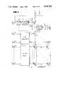
- FIG. 1is a circuit diagram representing a prior art programming operation
- FIG. 2is a graph showing a voltage-current characteristic of the circuit shown in FIG. 1;
- FIG. 3is a circuit diagram representing a programming operation of the present invention.
- FIG. 4is a graph showing a voltage-current characteristic of the circuit shown in FIG. 3;
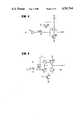
- FIG. 5is a diagram showing a preferred embodiment of the present invention.
- FIG. 6is a circuit diagram of a writing signal producing circuit shown in FIG. 5;
- FIG. 7is a circuit diagram of a read-out circuit shown in FIG. 5.
- a memory cell MCis composed of a transistor Q 1 of an N-channel type having a floating gate 1-4.
- a transistor Q 2 of the same channel (N-channel) type as the transistor Q 1is connected in series to Q 1 .
- a writing signal Wis supplied to the gate 2-3 of the transistor Q 2 , the drain 2-2 of which is connected to a terminal 3 supplied with a programming voltage V pp .
- the writing signal Wdepends on a data to be programmed and thus takes a V pp level when the data is "1", for example, and a zero volt level when it is "0".
- the source 1-1 of the memory cell transistor Q 1is grounded and the control gate 1-3 thereof is supplied with a selection signal X from a decoder (not shown).
- the drain 102 of the transistor Q 1is connected to the source 2-1 of the transistor Q 1 , this connection point being represented by "a".
- the programming voltage V ppis applied to the terminal 3 and the writing signal W assumes the V pp level to turn the transistor Q 1 ON. Consequently, the voltage V a at the point a takes a high voltage responsive to the V pp voltage.
- the selection signal Xis at the V pp level.
- the drain 1-1 and the control gate 1-3 of the memory cell transistor Q 1receive high voltages, so that electrons are injected into the floating gate 1-4 of Q 1 .
- the floating gate 1-4is thereby charged to a negative potential to increase a threshold voltage of the transistor Q 1 .
- the transistor Q 2Since the transistor Q 2 is of an N-channel type, it has a linear load characteristic represented by a line 30 in FIG. 2.
- an abscissais a voltage V a at the point a and an ordinate is a current I 1 flowing through the transistors Q 1 and Q 2 .
- a voltage-current characteristic of the memory cell transistor Q 1 before a programmingis represented by a line 10 in FIG. 2. Accordingly, when the voltage V a at the point a becomes larger than a voltage V W1 represented as an intersection of the lines 10 and 30, the transistor Q 1 is supplied with a current I W1 to inject electrons into the floating gate 1-4 of Q 1 . A programmed memory cell is thus obtained.
- the memory cell transistor Q 1When the memory cell transistor Q 1 is brought into the programmed condition, its voltage-current characteristic is changed to a line 20 shown in FIG. 2. That is, since the floating gate assumes a negative potential and the drain 1-2 is applied with a high voltage, a high electric field occurs near the drain 1-2 to cause a channel breakdown in the transistor Q 1 . In other words, the programmed memory cell transistor Q 1 . In other words, the programmed memory cell transistor Q 1 represents a negative resistance at a voltage RV. As a result, the voltage V a at the point a is lowered to a value V W2 and the current I 1 is increased to a value I W2 . The current value I W2 is considerably larger than the value I W1 . A power consumption (I W2 ⁇ V pp ) at this time is a part of a programming power consumption.
- FIG. 3shows a circuit diagram representing a programming operation of the present invention.
- the memory cell transistor Q 1is supplied with a programming current through a transistor Q 3 that is of an opposite conductivity type to the transistor Q 1 , i.e., a P-channel type. Therefore, the source 3-1 of Q 3 is connected to the terminal 3 along with its substrate electrode, and the drain 3-2 thereof is connected to the drain 1-2 of Q 1 .
- the connection point of the drains of the transistors Q 1 and Q 3is represented by "b".
- the transistor Q 3is driven by a writing signal W which has an amplitude that is approximately equal to a potential difference between the programming voltage V pp and a selection voltage supplied to the memory cell in a read-out operation.
- a P-channel transistor Q 5 and an N-channel transistor Q 4are connected in series between terminals 3 and 4, and the connection point therebetween is connected to the gate 3-3 of the transistor Q 3 .
- a writing control signal WC responsive to an input datais supplied in common to the gates of Q 4 and Q 5 .
- the terminal 4is supplied with a voltage of a V cc level. This voltage level is substantially equal to the selection level supplied to the memory cell in the read-out operation.
- the transistor Q 3Since the transistor Q 3 is of a P-channel type and the source 3-1 thereof is connected to the terminal 3, Q 3 represents a constant current characteristic when its gate-source voltage V GS is smaller in absolute value than its source-drain voltage V DS and a resistive characteristic when V GS is larger in absolute value than V DS . Therefore, the load characteristic of the transistor Q 3 is completely different from that of the transistor Q 2 (FIG. 1) and is shown by a line 40 in FIG. 4. An abscissa of a graph in FIG. 4 is a voltage V b at the point b and an ordinate thereof is a current I 2 flowing through the transistors Q 1 and Q 3 . The voltage-current characteristics of the memory cell transistor Q 1 before a programming and after it are not changed, as represented by lines 10 and 20 in FIG. 4, respectively.
- the point btherefore assumes a voltage V W3 which is represented as an intersection of the lines 10 and 40 and the programming current I 2 having a value I W3 flows through the transistor Q 1 .
- the transistor Q 3is supplied at its gate 3-3 with the V cc level, not with the ground level. Therefore, the constant current characteristic region of the transistor Q 3 is broadened, the current value I W3 required for the programming is supplied surely to the transistor Q 1 .
- the programming memory cell transistor Q 1represents the negative resistance as mentioned hereinbefore, so that the voltage V b is lowered from the value V W3 to a value V W4 .
- the constant current characteristic of the transistor Q 3maintains the current I 2 flowing through the transistors Q 1 and Q 3 at the value I W3 . The programming power consumption is thereby reduced remarkably.
- the writing control signal WCtakes O v as its low level and V pp level as its high level, and the writing signal W takes V cc level as its low level and the V pp level as its high level. Therefore, the transistors Q 4 and Q 5 operate as a level conversion circuit.
- FIG. 5shows a semiconductor memory according to one embodiment of the present invention, in which the same constituents as those shown in FIG. 3 are denoted by like references.
- Each of a plurality of N-channel transistors Q 11 to Q NMhas a floating gate and constitutes a memory cell. These transistors Q 11 to Q NM are arranged in rows and columns to form a memory cell array 62.
- the drains of the memory cell transistors disposed in the same columnare connected in common to one of digit lines D 1 to D M , and the control gates of the memory cell transistors disposed in the same row are connected in common to one of word lines W 1 to W N .
- the sources of the transistors Q 11 to Q NMare connected to a reference potential (a ground potential, in this embodiment).
- the digit lines D 1 to D Mare connected to a circuit node N through N-channel switching transistors Q 201 to Q 20M , respectively.
- Row address signals RA O to RA iare supplied through row address terminals 61-O to 61-i to a row decoder 63, and column address signals CA O to CA j are supplied through column address terminals 60-O to 60-j to a column decoder 64.
- the row decoder 63applies a selection level to one of row selection signal X 1 to X N .
- One of the word lines W 1 to W Nis thereby energized.
- the column decoder 64raises one of column selection signal Y 1 to Y M to the selection level.
- the associated one of the transistors Q 201 to Q 20Mis turned ON to energized one of the digit lines D 1 to D M .
- the memory cell corresponding to the row and column address signals CA and RAis thus selected.
- a transistor Q 3 of an opposite conductivity type as the memory cell transistor(i.e., a P-channel type) is provided between the circuit node N and a terminal 3 in accordance with the present invention.
- the transistor Q 3is driven by transistors Q 4 and Q 5 connected in series between the terminals 3 and 4.
- the writing control signal WC supplied to the gates of Q 4 and Q 5is produced by a writing signal producing circuit 66.
- a write-enable signal WE supplied theretois inverted by an inverter 661 and the inverted signal is supplied through an N-channel transistor Q 661 to the gates of a P-channel transistor Q 663 and an N-channel transistor Q 664 .
- the transistors Q 663 and Q 664are connected in series between the terminal 3 and the ground, and the signal WC is produced the connection point thereof.
- the signal WCis fed back to a P-channel transistor Q 662 .
- the writing signal producing circuit 66determines the level of the writing control signal WC in response to the level of the write-enable signal WE.
- the signal WCtakes either one of O v and V pp .
- This signalis converted into the signal W taking either one of V cc and V pp by the transistors Q 5 and Q 4 .
- V ppis larger in absolute value than V cc .
- the write-enable signal WEis produced by a writing control circuit 65.
- This circuit 65responds to a programming control signal PC supplied to a terminal 50 and carries out a programming operation or a read-out operation.
- the terminal 3is applied with the V pp level and the terminal 50 is supplied with the programming signal having a high level, for example.
- the writing control circuit 65determines the level of the signal WE in response to an input data supplied to a terminal 69.
- the circuit 65further supplies a signal RE having its level that inactivates a read-out circuit 67.
- the transistor Q 3is supplied with V cc level and thus turned ON.
- the row and column decoderraise ones of the row and column selection signals X and Y to the selection level.
- This selection leveltakes the V pp level in the programming operation.
- the programming voltage and currentare thus supplied through the transistor Q 3 to the selected memory cell to carry out the programming thereto.
- the programming power consumption in this operationis remarkably small as explained with reference to FIGS. 3 and 4.
- the terminal 3is connected to the terminal 4 to receive the V cc level, and the low level signal PC is supplied to the terminal 50.
- the writing control circuit 65changes the signal WE to a level that maintains the transistor Q 3 in an off-state and produces a read-enable signal RE to the read-out circuit 67.
- One of the row selection signals X and one of column selection signals Yare raised to a selection level in response to address signals RA and CA.
- the selection level at this timeassumes about V cc level since the terminal 3 receives the V cc level.
- the programmed memory cellis selected, this cell is maintained in the off-state, since its threshold voltage is higher than the selection level of the signal X.
- the unprogrammed memory cellis selected, it is turned ON to lower the potential at the node N.
- the potential at the node Nis supplied to the read-out circuit 67 as a cell data.
- the read-out circuit 67includes N-channel transistors Q 673 and Q 674 connected in a differential form.
- the gate of the transistor Q 673is connected to the circuit node N through an N-channel transistor Q 671 , and the gate of the transistor Q 674 is supplied with a reference voltage V REF .
- An N-channel transistor Q 675 operating as a current sourceis connected to the source connection point of Q 673 and Q 674 .
- P-channel transistors Q 676 and Q 677constitute a current mirror load, and from the connection point of the transistors Q 677 and Q 674 a read-out data DO supplied to a data output circuit 68 (FIG. 5) is derived.
- the transistors Q 671 and Q 675are supplied at their gates with the read-enable signal RE.
- the signal REtakes the low level in the programming operation to inactivate the read-out circuit 67 and assumes the high level in the read-out operation to turn the transistors Q 671 and Q 675 ON.
- the circuit 67is thereby activated.
- the circuit node NWhen the programmed memory cell is selected, the circuit node N is disconnected from the ground. However, a P-channel transistor Q 672 is provided, and therefore the gate of the transistor Q 673 receives a high voltage.
- the reference voltage V REF supplied to the transistor Q 674is selected to an intermediate level between the above-mentioned high voltage and the resistance divided voltage.
- the read-out data DOtakes the high level or the low level in response to the programmed cell or the unprogrammed cell, respectively.
- the read-out data DOis supplied to the data output circuit 68, so that an output data D OUT is derived from the terminal 69.
- the terminal 69is thus used as a data input/output terminal.
- the present inventionis not limited to the above-described embodiment, but may be changed and modified without departing from the scope and spirit of the present invention.
- a plurality of terminals 69can be provided.
Landscapes
- Read Only Memory (AREA)
- Semiconductor Memories (AREA)
Abstract
Description
Claims (7)
Applications Claiming Priority (2)
| Application Number | Priority Date | Filing Date | Title |
|---|---|---|---|
| JP8275685 | 1985-04-18 | ||
| JP60-82756 | 1985-04-18 |
Publications (1)
| Publication Number | Publication Date |
|---|---|
| US4761764Atrue US4761764A (en) | 1988-08-02 |
Family
ID=13783281
Family Applications (1)
| Application Number | Title | Priority Date | Filing Date |
|---|---|---|---|
| US06/853,509Expired - LifetimeUS4761764A (en) | 1985-04-18 | 1986-04-18 | Programmable read only memory operable with reduced programming power consumption |
Country Status (4)
| Country | Link |
|---|---|
| US (1) | US4761764A (en) |
| EP (1) | EP0199305B1 (en) |
| JP (1) | JPH0770230B2 (en) |
| DE (1) | DE3684351D1 (en) |
Cited By (49)
| Publication number | Priority date | Publication date | Assignee | Title |
|---|---|---|---|---|
| US4823318A (en)* | 1988-09-02 | 1989-04-18 | Texas Instruments Incorporated | Driving circuitry for EEPROM memory cell |
| US4829203A (en)* | 1988-04-20 | 1989-05-09 | Texas Instruments Incorporated | Integrated programmable bit circuit with minimal power requirement |
| US4858187A (en)* | 1988-02-01 | 1989-08-15 | Texas Instruments Incorporated | Programming implementation circuit |
| US4910710A (en)* | 1987-11-25 | 1990-03-20 | Nec Corporation | Input circuit incorporated in a semiconductor device |
| US4977541A (en)* | 1988-06-17 | 1990-12-11 | Motorola, Inc. | EPROM programming |
| US5010520A (en)* | 1987-07-29 | 1991-04-23 | Kabushiki Kaisha Toshiba | Nonvolatile semiconductor memory device with stabilized data write characteristic |
| US5016218A (en)* | 1987-11-24 | 1991-05-14 | Kabushiki Kaisha Toshiba | Nonvolatile memory with data write circuitry to reduce write errors |
| US5050124A (en)* | 1986-09-30 | 1991-09-17 | Kabushiki Kaisha Toshiba | Semiconductor memory having load transistor circuit |
| US5105384A (en)* | 1987-04-08 | 1992-04-14 | Mitsubishi Denki Kabushiki Kaisha | Low current semiconductor memory device |
| US5265052A (en)* | 1989-07-20 | 1993-11-23 | Texas Instruments Incorporated | Wordline driver circuit for EEPROM memory cell |
| US5619450A (en)* | 1991-12-09 | 1997-04-08 | Fujitsu Limited | Drive circuit for flash memory with improved erasability |
| US5859798A (en)* | 1996-09-24 | 1999-01-12 | Sgs-Thomson Microelectronics S.A. | Read circuit for non-volatile memory working with a low supply voltage |
| US6021083A (en)* | 1997-12-05 | 2000-02-01 | Macronix International Co., Ltd. | Block decoded wordline driver with positive and negative voltage modes |
| US6058934A (en)* | 1995-11-02 | 2000-05-09 | Chiron Diagnostics Corporation | Planar hematocrit sensor incorporating a seven-electrode conductivity measurement cell |
| US20020194422A1 (en)* | 2001-04-05 | 2002-12-19 | Zeev Cohen | Method and apparatus for dynamically masking an N-bit memory array having individually programmable cells |
| US20040153620A1 (en)* | 2003-01-30 | 2004-08-05 | Shai Eisen | Address scramble |
| US20050058005A1 (en)* | 2002-01-31 | 2005-03-17 | Assaf Shappir | Method for operating a memory device |
| US20050117395A1 (en)* | 2002-01-31 | 2005-06-02 | Saifun Semiconductors Ltd. | Method for operating a memory device |
| US6917544B2 (en) | 2002-07-10 | 2005-07-12 | Saifun Semiconductors Ltd. | Multiple use memory chip |
| US6928001B2 (en) | 2000-12-07 | 2005-08-09 | Saifun Semiconductors Ltd. | Programming and erasing methods for a non-volatile memory cell |
| US20050276118A1 (en)* | 2004-06-10 | 2005-12-15 | Eduardo Maayan | Reduced power programming of non-volatile cells |
| US7064983B2 (en) | 2001-04-05 | 2006-06-20 | Saifum Semiconductors Ltd. | Method for programming a reference cell |
| US7136304B2 (en) | 2002-10-29 | 2006-11-14 | Saifun Semiconductor Ltd | Method, system and circuit for programming a non-volatile memory array |
| US20070064484A1 (en)* | 2005-09-21 | 2007-03-22 | Actel Corporation, A California Corporation | Non-volatile programmable memory cell for programmable logic array |
| US7221138B2 (en) | 2005-09-27 | 2007-05-22 | Saifun Semiconductors Ltd | Method and apparatus for measuring charge pump output current |
| US7317633B2 (en) | 2004-07-06 | 2008-01-08 | Saifun Semiconductors Ltd | Protection of NROM devices from charge damage |
| US7352627B2 (en) | 2006-01-03 | 2008-04-01 | Saifon Semiconductors Ltd. | Method, system, and circuit for operating a non-volatile memory array |
| US7369440B2 (en) | 2005-01-19 | 2008-05-06 | Saifun Semiconductors Ltd. | Method, circuit and systems for erasing one or more non-volatile memory cells |
| US7405969B2 (en) | 1997-08-01 | 2008-07-29 | Saifun Semiconductors Ltd. | Non-volatile memory cell and non-volatile memory devices |
| US7457183B2 (en) | 2003-09-16 | 2008-11-25 | Saifun Semiconductors Ltd. | Operating array cells with matched reference cells |
| US7466594B2 (en) | 2004-08-12 | 2008-12-16 | Saifun Semiconductors Ltd. | Dynamic matching of signal path and reference path for sensing |
| US7532529B2 (en) | 2004-03-29 | 2009-05-12 | Saifun Semiconductors Ltd. | Apparatus and methods for multi-level sensing in a memory array |
| US7535765B2 (en) | 2004-12-09 | 2009-05-19 | Saifun Semiconductors Ltd. | Non-volatile memory device and method for reading cells |
| US7590001B2 (en) | 2007-12-18 | 2009-09-15 | Saifun Semiconductors Ltd. | Flash memory with optimized write sector spares |
| US7605579B2 (en) | 2006-09-18 | 2009-10-20 | Saifun Semiconductors Ltd. | Measuring and controlling current consumption and output current of charge pumps |
| US7638835B2 (en) | 2006-02-28 | 2009-12-29 | Saifun Semiconductors Ltd. | Double density NROM with nitride strips (DDNS) |
| US7638850B2 (en) | 2004-10-14 | 2009-12-29 | Saifun Semiconductors Ltd. | Non-volatile memory structure and method of fabrication |
| US7652930B2 (en) | 2004-04-01 | 2010-01-26 | Saifun Semiconductors Ltd. | Method, circuit and system for erasing one or more non-volatile memory cells |
| US7668017B2 (en) | 2005-08-17 | 2010-02-23 | Saifun Semiconductors Ltd. | Method of erasing non-volatile memory cells |
| US7692961B2 (en) | 2006-02-21 | 2010-04-06 | Saifun Semiconductors Ltd. | Method, circuit and device for disturb-control of programming nonvolatile memory cells by hot-hole injection (HHI) and by channel hot-electron (CHE) injection |
| US7701779B2 (en) | 2006-04-27 | 2010-04-20 | Sajfun Semiconductors Ltd. | Method for programming a reference cell |
| US7743230B2 (en) | 2003-01-31 | 2010-06-22 | Saifun Semiconductors Ltd. | Memory array programming circuit and a method for using the circuit |
| US7760554B2 (en) | 2006-02-21 | 2010-07-20 | Saifun Semiconductors Ltd. | NROM non-volatile memory and mode of operation |
| USRE41485E1 (en)* | 1993-09-21 | 2010-08-10 | Kabushiki Kaisha Toshiba | Multi-state EEPROM having write-verify control circuit |
| US7786512B2 (en) | 2005-07-18 | 2010-08-31 | Saifun Semiconductors Ltd. | Dense non-volatile memory array and method of fabrication |
| US7808818B2 (en) | 2006-01-12 | 2010-10-05 | Saifun Semiconductors Ltd. | Secondary injection for NROM |
| US8053812B2 (en) | 2005-03-17 | 2011-11-08 | Spansion Israel Ltd | Contact in planar NROM technology |
| US8253452B2 (en) | 2006-02-21 | 2012-08-28 | Spansion Israel Ltd | Circuit and method for powering up an integrated circuit and an integrated circuit utilizing same |
| US8400841B2 (en) | 2005-06-15 | 2013-03-19 | Spansion Israel Ltd. | Device to program adjacent storage cells of different NROM cells |
Families Citing this family (4)
| Publication number | Priority date | Publication date | Assignee | Title |
|---|---|---|---|---|
| JPH0754636B2 (en)* | 1987-07-30 | 1995-06-07 | 日本電気株式会社 | Nonvolatile semiconductor memory device |
| JPH0793018B2 (en)* | 1988-03-14 | 1995-10-09 | 株式会社東芝 | Non-volatile semiconductor memory |
| JPH08293197A (en)* | 1995-04-21 | 1996-11-05 | Nec Corp | Non-volatile semiconductor memory |
| US8331084B2 (en) | 2010-05-13 | 2012-12-11 | General Electric Company | Apparatus for securing electronic equipment |
Citations (2)
| Publication number | Priority date | Publication date | Assignee | Title |
|---|---|---|---|---|
| US4103185A (en)* | 1976-03-04 | 1978-07-25 | Rca Corporation | Memory cells |
| US4228527A (en)* | 1978-02-22 | 1980-10-14 | Centre Electronique Horloger S.A. | Electrically reprogrammable non volatile memory |
Family Cites Families (6)
| Publication number | Priority date | Publication date | Assignee | Title |
|---|---|---|---|---|
| US4128773A (en)* | 1977-11-07 | 1978-12-05 | Hughes Aircraft Company | Volatile/non-volatile logic latch circuit |
| US4142251A (en)* | 1977-11-21 | 1979-02-27 | Hewlett-Packard Company | Field programmable read-only-memory |
| JPS5753152A (en)* | 1980-09-16 | 1982-03-30 | Nec Ic Microcomput Syst Ltd | Inverter circuit |
| JPS5850700A (en)* | 1981-09-21 | 1983-03-25 | Hitachi Ltd | EPROM writing circuit |
| US4464221A (en)* | 1983-01-28 | 1984-08-07 | Dynachem Corporation | Automatic laminator |
| JPH0666115B2 (en)* | 1983-09-26 | 1994-08-24 | 株式会社東芝 | Semiconductor memory device |
- 1986
- 1986-04-18USUS06/853,509patent/US4761764A/ennot_activeExpired - Lifetime
- 1986-04-18EPEP86105377Apatent/EP0199305B1/ennot_activeExpired - Lifetime
- 1986-04-18DEDE8686105377Tpatent/DE3684351D1/ennot_activeExpired - Lifetime
- 1986-04-18JPJP9075886Apatent/JPH0770230B2/ennot_activeExpired - Fee Related
Patent Citations (2)
| Publication number | Priority date | Publication date | Assignee | Title |
|---|---|---|---|---|
| US4103185A (en)* | 1976-03-04 | 1978-07-25 | Rca Corporation | Memory cells |
| US4228527A (en)* | 1978-02-22 | 1980-10-14 | Centre Electronique Horloger S.A. | Electrically reprogrammable non volatile memory |
Cited By (63)
| Publication number | Priority date | Publication date | Assignee | Title |
|---|---|---|---|---|
| US5050124A (en)* | 1986-09-30 | 1991-09-17 | Kabushiki Kaisha Toshiba | Semiconductor memory having load transistor circuit |
| US5105384A (en)* | 1987-04-08 | 1992-04-14 | Mitsubishi Denki Kabushiki Kaisha | Low current semiconductor memory device |
| US5010520A (en)* | 1987-07-29 | 1991-04-23 | Kabushiki Kaisha Toshiba | Nonvolatile semiconductor memory device with stabilized data write characteristic |
| US5016218A (en)* | 1987-11-24 | 1991-05-14 | Kabushiki Kaisha Toshiba | Nonvolatile memory with data write circuitry to reduce write errors |
| US4910710A (en)* | 1987-11-25 | 1990-03-20 | Nec Corporation | Input circuit incorporated in a semiconductor device |
| US4858187A (en)* | 1988-02-01 | 1989-08-15 | Texas Instruments Incorporated | Programming implementation circuit |
| US4829203A (en)* | 1988-04-20 | 1989-05-09 | Texas Instruments Incorporated | Integrated programmable bit circuit with minimal power requirement |
| US4977541A (en)* | 1988-06-17 | 1990-12-11 | Motorola, Inc. | EPROM programming |
| US4823318A (en)* | 1988-09-02 | 1989-04-18 | Texas Instruments Incorporated | Driving circuitry for EEPROM memory cell |
| US5265052A (en)* | 1989-07-20 | 1993-11-23 | Texas Instruments Incorporated | Wordline driver circuit for EEPROM memory cell |
| US5619450A (en)* | 1991-12-09 | 1997-04-08 | Fujitsu Limited | Drive circuit for flash memory with improved erasability |
| USRE41485E1 (en)* | 1993-09-21 | 2010-08-10 | Kabushiki Kaisha Toshiba | Multi-state EEPROM having write-verify control circuit |
| US6058934A (en)* | 1995-11-02 | 2000-05-09 | Chiron Diagnostics Corporation | Planar hematocrit sensor incorporating a seven-electrode conductivity measurement cell |
| US5859798A (en)* | 1996-09-24 | 1999-01-12 | Sgs-Thomson Microelectronics S.A. | Read circuit for non-volatile memory working with a low supply voltage |
| US7405969B2 (en) | 1997-08-01 | 2008-07-29 | Saifun Semiconductors Ltd. | Non-volatile memory cell and non-volatile memory devices |
| US6021083A (en)* | 1997-12-05 | 2000-02-01 | Macronix International Co., Ltd. | Block decoded wordline driver with positive and negative voltage modes |
| US6937521B2 (en) | 2000-05-04 | 2005-08-30 | Saifun Semiconductors Ltd. | Programming and erasing methods for a non-volatile memory cell |
| US6928001B2 (en) | 2000-12-07 | 2005-08-09 | Saifun Semiconductors Ltd. | Programming and erasing methods for a non-volatile memory cell |
| US6665769B2 (en)* | 2001-04-05 | 2003-12-16 | Saifun Semiconductors Ltd. | Method and apparatus for dynamically masking an N-bit memory array having individually programmable cells |
| US7064983B2 (en) | 2001-04-05 | 2006-06-20 | Saifum Semiconductors Ltd. | Method for programming a reference cell |
| US20020194422A1 (en)* | 2001-04-05 | 2002-12-19 | Zeev Cohen | Method and apparatus for dynamically masking an N-bit memory array having individually programmable cells |
| US7079420B2 (en) | 2002-01-31 | 2006-07-18 | Saifun Semiconductors Ltd. | Method for operating a memory device |
| US7420848B2 (en) | 2002-01-31 | 2008-09-02 | Saifun Semiconductors Ltd. | Method, system, and circuit for operating a non-volatile memory array |
| US20050058005A1 (en)* | 2002-01-31 | 2005-03-17 | Assaf Shappir | Method for operating a memory device |
| US7190620B2 (en) | 2002-01-31 | 2007-03-13 | Saifun Semiconductors Ltd. | Method for operating a memory device |
| US20050117395A1 (en)* | 2002-01-31 | 2005-06-02 | Saifun Semiconductors Ltd. | Method for operating a memory device |
| US7738304B2 (en) | 2002-07-10 | 2010-06-15 | Saifun Semiconductors Ltd. | Multiple use memory chip |
| US6917544B2 (en) | 2002-07-10 | 2005-07-12 | Saifun Semiconductors Ltd. | Multiple use memory chip |
| US7136304B2 (en) | 2002-10-29 | 2006-11-14 | Saifun Semiconductor Ltd | Method, system and circuit for programming a non-volatile memory array |
| US7675782B2 (en) | 2002-10-29 | 2010-03-09 | Saifun Semiconductors Ltd. | Method, system and circuit for programming a non-volatile memory array |
| US6967896B2 (en) | 2003-01-30 | 2005-11-22 | Saifun Semiconductors Ltd | Address scramble |
| US20040153620A1 (en)* | 2003-01-30 | 2004-08-05 | Shai Eisen | Address scramble |
| US7743230B2 (en) | 2003-01-31 | 2010-06-22 | Saifun Semiconductors Ltd. | Memory array programming circuit and a method for using the circuit |
| US7457183B2 (en) | 2003-09-16 | 2008-11-25 | Saifun Semiconductors Ltd. | Operating array cells with matched reference cells |
| US7532529B2 (en) | 2004-03-29 | 2009-05-12 | Saifun Semiconductors Ltd. | Apparatus and methods for multi-level sensing in a memory array |
| US7652930B2 (en) | 2004-04-01 | 2010-01-26 | Saifun Semiconductors Ltd. | Method, circuit and system for erasing one or more non-volatile memory cells |
| US7366025B2 (en) | 2004-06-10 | 2008-04-29 | Saifun Semiconductors Ltd. | Reduced power programming of non-volatile cells |
| US20050276118A1 (en)* | 2004-06-10 | 2005-12-15 | Eduardo Maayan | Reduced power programming of non-volatile cells |
| US7317633B2 (en) | 2004-07-06 | 2008-01-08 | Saifun Semiconductors Ltd | Protection of NROM devices from charge damage |
| US7466594B2 (en) | 2004-08-12 | 2008-12-16 | Saifun Semiconductors Ltd. | Dynamic matching of signal path and reference path for sensing |
| US7964459B2 (en) | 2004-10-14 | 2011-06-21 | Spansion Israel Ltd. | Non-volatile memory structure and method of fabrication |
| US7638850B2 (en) | 2004-10-14 | 2009-12-29 | Saifun Semiconductors Ltd. | Non-volatile memory structure and method of fabrication |
| US7535765B2 (en) | 2004-12-09 | 2009-05-19 | Saifun Semiconductors Ltd. | Non-volatile memory device and method for reading cells |
| US7468926B2 (en) | 2005-01-19 | 2008-12-23 | Saifun Semiconductors Ltd. | Partial erase verify |
| US7369440B2 (en) | 2005-01-19 | 2008-05-06 | Saifun Semiconductors Ltd. | Method, circuit and systems for erasing one or more non-volatile memory cells |
| US8053812B2 (en) | 2005-03-17 | 2011-11-08 | Spansion Israel Ltd | Contact in planar NROM technology |
| US8400841B2 (en) | 2005-06-15 | 2013-03-19 | Spansion Israel Ltd. | Device to program adjacent storage cells of different NROM cells |
| US7786512B2 (en) | 2005-07-18 | 2010-08-31 | Saifun Semiconductors Ltd. | Dense non-volatile memory array and method of fabrication |
| US7668017B2 (en) | 2005-08-17 | 2010-02-23 | Saifun Semiconductors Ltd. | Method of erasing non-volatile memory cells |
| US20070230244A1 (en)* | 2005-09-21 | 2007-10-04 | Actel Corporation | Non-volatile programmable memory cell for programmable logic array |
| US7590000B2 (en) | 2005-09-21 | 2009-09-15 | Actel Corporation | Non-volatile programmable memory cell for programmable logic array |
| US20070064484A1 (en)* | 2005-09-21 | 2007-03-22 | Actel Corporation, A California Corporation | Non-volatile programmable memory cell for programmable logic array |
| US7245535B2 (en)* | 2005-09-21 | 2007-07-17 | Actel Corporation | Non-volatile programmable memory cell for programmable logic array |
| US7221138B2 (en) | 2005-09-27 | 2007-05-22 | Saifun Semiconductors Ltd | Method and apparatus for measuring charge pump output current |
| US7352627B2 (en) | 2006-01-03 | 2008-04-01 | Saifon Semiconductors Ltd. | Method, system, and circuit for operating a non-volatile memory array |
| US7808818B2 (en) | 2006-01-12 | 2010-10-05 | Saifun Semiconductors Ltd. | Secondary injection for NROM |
| US8253452B2 (en) | 2006-02-21 | 2012-08-28 | Spansion Israel Ltd | Circuit and method for powering up an integrated circuit and an integrated circuit utilizing same |
| US7692961B2 (en) | 2006-02-21 | 2010-04-06 | Saifun Semiconductors Ltd. | Method, circuit and device for disturb-control of programming nonvolatile memory cells by hot-hole injection (HHI) and by channel hot-electron (CHE) injection |
| US7760554B2 (en) | 2006-02-21 | 2010-07-20 | Saifun Semiconductors Ltd. | NROM non-volatile memory and mode of operation |
| US7638835B2 (en) | 2006-02-28 | 2009-12-29 | Saifun Semiconductors Ltd. | Double density NROM with nitride strips (DDNS) |
| US7701779B2 (en) | 2006-04-27 | 2010-04-20 | Sajfun Semiconductors Ltd. | Method for programming a reference cell |
| US7605579B2 (en) | 2006-09-18 | 2009-10-20 | Saifun Semiconductors Ltd. | Measuring and controlling current consumption and output current of charge pumps |
| US7590001B2 (en) | 2007-12-18 | 2009-09-15 | Saifun Semiconductors Ltd. | Flash memory with optimized write sector spares |
Also Published As
| Publication number | Publication date |
|---|---|
| JPS6231097A (en) | 1987-02-10 |
| EP0199305A3 (en) | 1988-12-14 |
| EP0199305A2 (en) | 1986-10-29 |
| EP0199305B1 (en) | 1992-03-18 |
| JPH0770230B2 (en) | 1995-07-31 |
| DE3684351D1 (en) | 1992-04-23 |
Similar Documents
| Publication | Publication Date | Title |
|---|---|---|
| US4761764A (en) | Programmable read only memory operable with reduced programming power consumption | |
| US5039882A (en) | Address decoder circuit for non-volatile memory | |
| US5276646A (en) | High voltage generating circuit for a semiconductor memory circuit | |
| US5717640A (en) | ROM type semiconductor memory device with large operating margin | |
| US4769787A (en) | Semiconductor memory device | |
| US4710900A (en) | Non-volatile semiconductor memory device having an improved write circuit | |
| US5058063A (en) | Nonvolatile semiconductor memory device incorporating level shifting circuits | |
| US5859798A (en) | Read circuit for non-volatile memory working with a low supply voltage | |
| EP0211232B1 (en) | Semiconductor memory in which data readout operation is carried out over wide power voltage range | |
| US4874967A (en) | Low power voltage clamp circuit | |
| JPH05250888A (en) | Level shifter circuit | |
| US4374430A (en) | Semiconductor PROM device | |
| US5610860A (en) | Integrated circuit memory with column voltage holding circuit | |
| US4635229A (en) | Semiconductor memory device including non-volatile transistor for storing data in a bistable circuit | |
| EP0332135B1 (en) | Nonvolatile memory circuit device with low power consumption and wide operating voltage range | |
| US5051956A (en) | Memory cell having means for maintaining the gate and substrate at the same potential | |
| US7355903B2 (en) | Semiconductor device including memory cells and current limiter | |
| KR0147240B1 (en) | Semiconductor memory device having a bias control circuit for erase voltage blocking transistor | |
| EP0377840B1 (en) | Nonvolatile semiconductor memory device having reference potential generating circuit | |
| US5038327A (en) | Decoder circuit of erasable programmable read only memory for avoiding erroneous operation caused by parasitic capacitors | |
| US5719490A (en) | Dual sourced voltage supply circuit | |
| US5691944A (en) | Non-volatile semiconductor memory device | |
| US5198998A (en) | Erasable programmable read only memory | |
| EP0520357B1 (en) | Read only memory device with recharging transistor automatically supplementing current to an input node of output inverter | |
| US6028793A (en) | High voltage driver circuit for a decoding circuit in multilevel non-volatile memory devices |
Legal Events
| Date | Code | Title | Description |
|---|---|---|---|
| AS | Assignment | Owner name:NEC CORPORATION, 33-1, SHHIBA 5-CHOME, MINATO-KU, Free format text:ASSIGNMENT OF ASSIGNORS INTEREST.;ASSIGNOR:WATANABE, TAKESHI;REEL/FRAME:004887/0806 Effective date:19860417 Owner name:NEC CORPORATION,JAPAN Free format text:ASSIGNMENT OF ASSIGNORS INTEREST;ASSIGNOR:WATANABE, TAKESHI;REEL/FRAME:004887/0806 Effective date:19860417 | |
| STCF | Information on status: patent grant | Free format text:PATENTED CASE | |
| CC | Certificate of correction | ||
| FEPP | Fee payment procedure | Free format text:PAYOR NUMBER ASSIGNED (ORIGINAL EVENT CODE: ASPN); ENTITY STATUS OF PATENT OWNER: LARGE ENTITY | |
| FPAY | Fee payment | Year of fee payment:4 | |
| FEPP | Fee payment procedure | Free format text:PAYOR NUMBER ASSIGNED (ORIGINAL EVENT CODE: ASPN); ENTITY STATUS OF PATENT OWNER: LARGE ENTITY Free format text:PAYER NUMBER DE-ASSIGNED (ORIGINAL EVENT CODE: RMPN); ENTITY STATUS OF PATENT OWNER: LARGE ENTITY | |
| FPAY | Fee payment | Year of fee payment:8 | |
| FEPP | Fee payment procedure | Free format text:PAYER NUMBER DE-ASSIGNED (ORIGINAL EVENT CODE: RMPN); ENTITY STATUS OF PATENT OWNER: LARGE ENTITY | |
| FPAY | Fee payment | Year of fee payment:12 | |
| AS | Assignment | Owner name:NEC ELECTRONICS CORPORATION, JAPAN Free format text:ASSIGNMENT OF ASSIGNORS INTEREST;ASSIGNOR:NEC CORPORATION;REEL/FRAME:013758/0440 Effective date:20021101 |