US4761736A - Memory management unit for addressing an expanded memory in groups of non-contiguous blocks - Google Patents
Memory management unit for addressing an expanded memory in groups of non-contiguous blocksDownload PDFInfo
- Publication number
- US4761736A US4761736AUS06/815,695US81569586AUS4761736AUS 4761736 AUS4761736 AUS 4761736AUS 81569586 AUS81569586 AUS 81569586AUS 4761736 AUS4761736 AUS 4761736A
- Authority
- US
- United States
- Prior art keywords
- memory
- microprocessor
- decoder
- address bus
- bus
- Prior art date
- Legal status (The legal status is an assumption and is not a legal conclusion. Google has not performed a legal analysis and makes no representation as to the accuracy of the status listed.)
- Expired - Lifetime
Links
Images
Classifications
- G—PHYSICS
- G06—COMPUTING OR CALCULATING; COUNTING
- G06F—ELECTRIC DIGITAL DATA PROCESSING
- G06F12/00—Accessing, addressing or allocating within memory systems or architectures
- G06F12/02—Addressing or allocation; Relocation
- G06F12/06—Addressing a physical block of locations, e.g. base addressing, module addressing, memory dedication
- G06F12/0615—Address space extension
- G06F12/0623—Address space extension for memory modules
- G—PHYSICS
- G06—COMPUTING OR CALCULATING; COUNTING
- G06F—ELECTRIC DIGITAL DATA PROCESSING
- G06F12/00—Accessing, addressing or allocating within memory systems or architectures
- G06F12/02—Addressing or allocation; Relocation
- G06F12/0223—User address space allocation, e.g. contiguous or non contiguous base addressing
- G06F12/0292—User address space allocation, e.g. contiguous or non contiguous base addressing using tables or multilevel address translation means
Definitions
- the inventionrelates to translator circuits for accessing expanded memory locations in read only memory (ROM) and dynamic random access memory (RAM) from microprocessors originally designed to access limited electronic memory.
- ROMread only memory
- RAMdynamic random access memory
- microprocessorssuch as Commodore-MOS Technology model 6502 or Zilog Corporation model Z80. These microprocessors are 8-bit devices whose internal architecture is set up to access 64K bytes of electronic memory, either RAM or ROM. These microprocessors are both reliable and inexpensive to incorporate into any computing or controller system.
- a limitation, however, in their use in the pasthas been that expanded memory, when used with these microprocessors, has had to be magnetic medium, such as magnetic tape or disk or the like. The writing and reading of data from such peripheral storage has always been slow.
- a memory management unitas a high speed interface, between large amounts of electronic memory (ROM and RAM) and the 6502 and Z80 microprocessors or similar microprocessor units, whereby these microprocessors' ability to address only 64K of electronic memory is increased to plural units of 64K electronic memory. It is also desirable that such memory management unit operate in dual microprocessor systems.
- An object of the present inventionis to provide a memory management unit circuit as a programmable controller or translator circuit which accesses large amounts of electronic memory (RAM and ROM) in 64K units or “windows" from microprocessor memory addresses.
- RAM and ROMelectronic memory
- a second objectis to provide this circuit for use in either single or plural (i.e. dual) microprocessor systems whereby the circuit is compatible with the NMOS (N-type metal oxide semiconductor) LSI (large scale integrated) circuit implementation of the host system.
- NMOSN-type metal oxide semiconductor
- LSIlarge scale integrated
- a further objectis to provide this circuit with the ability to access the 64K memory window from units of 16K memory selected from between any of a plurality of RAM and ROM chips.
- An additional objectis to select between memory size for 40 column and 80 column video display.
- the objects of the present inventionare incorporated in a circuit implemented in NMOS, LSI circuitry on a 48 pin DIP (dual in line pin) chip wherein the operating status of the circuit is switched between predetermined operating states (functions) by program instructions loaded into registers, whereby these instructions operate functionally as switches for circuit operation selection.
- DIPdual in line pin
- a dual microprocessor systemincludes an 8-bit 6502 type microprocessor (or a similar Commodore-MOS Technology 8502 microprocessor) and an 8-bit Z80 microprocessor.
- a 16-bit address busis common to both microprocessors and an 8-bit data bus is likewise common to both microprocessors.
- a buffer circuitis used to interface the data bus to the Z80 microprocessor as the 8502 microprocessor is allowed to operate at a slower speed from the Z80.
- RAMdynamic random access memory
- ROMread only memory
- Memory addressesare received from either the 8502 or the Z80 via the address bus and translated into an expanded memory address which enables selected memory locations on the RAM chips to be available to the data bus during a particular processing cycle. Z80 and 8502 access on the data bus is controlled.
- the expanded memory addressis used to generate or control instruction which is input into a programmable logic array circuit (PLA).
- PLAprogrammable logic array circuit
- This PLAis implemented as a decoder circuit whose output is an exclusive control signal on one of a plurality of dedicated control lines to the 128K ROM chips.
- This decoder circuit outputselects one of the ROM chips to be available to the data bus during a particular processing cycle.
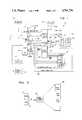
- FIG. 1is a circuit block diagram of a dual microprocessor system utilizing expanded electronic memory accessing in 64K memory units per processing cycle;
- FIG. 2is a functional operation diagram for the memory location translator component of the circuit of FIG. 1;
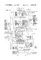
- FIG. 3is a circuit block diagram of the memory location translator component of the circuit of FIG. 1;
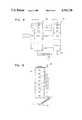
- FIG. 4is an illustration of RAMS 35 and 37 of FIG. 1;
- FIG. 5is an illustration of ROM 45 of FIG. 1.
- a personal computer system 10, FIG. 1,has dual microprocessors, a Commodore-MOS Technology model 8502 microprocessor 11, and a Zilog Corporation model Z80 microprocessor 13.
- a keyboard 15is connected to provide operator data and instructions to the 8502 microprocessor 11.
- a video/audio display 17is connected to the Z80 microprocessor 13 or the 8502 microprocessor 11 while other peripheral devices 19, including floppy disk and paddles, are connected to both microprocessors 11, 13.
- An oscillatorbeing the system clock 21, provides 4, 2 and 1 MHz pulses, where the Z80 microprocessor 13 is operated at the 4 MHz rate and the 8502 microprocessor 11 is operated at the 2 or 1 MHz rate.
- a 16-bit address bus 23is connected to each of the 8502 and Z80 microprocessors 11, 13 for bi-directional transmission of addresses.
- An 8-bit data bus 25is connected directly to the 8502 microprocessor 11 and to the Z80 microprocessor 13 through a data buffer 27 for bi-directional transmission of data.
- a memory translator and control circuit 29is connected to the data bus 25, and provides a (Z80 enable) select signal on line 31 to the Z80 microprocessor 13, its data buffer 27 and the 8502 microprocessor 11 to select between microprocessors 11 and 13 being on the system data bus 25.
- select signalis "high,” the Z80 microprocessor 13 is on and the 8502 microprocessor 11 is off the data bus 25.
- the memory translator and control circuit 29is also connected to the address bus 25.
- a program logic array (PLA) decoder circuit 33is connected to the address bus 23 and to the memory translator and control circuit 29.
- a first and second 64K dynamic random access memories (RAM) 35, 37are each connected to the memory translator and control circuit through a multiplexer/circuit 39.
- the multiplexer 39receives the 8 least significant bits 40 from the address bus 23 and 8-bit words 42 from the memory translator and control circuit 29 and transmits same to each RAM 35, 37 as 8-bit addresses.
- An exclusive column address strobe (CAS) select signals 41, 43is generated by the memory translator and control circuit 29 and connected to the RAMs 35, 37 with the CAS-0 signal 41 enabling the first RAM 35 and the CAS-1 signal 43 enabling the second RAM 37.
- Each of the RAMs 35, 37is connected for bi-directional transmission with the data bus 25.
- a plurality of 128K read only memories (ROM) 45are each connected to place data on the data bus 25 when enabled by an exclusive select signal 47 from the decoder 33.
- Each ROM 45is connected to the address bus 23.
- the decoder 33has seven select (ROM) control lines 47. This number of ROM memories can be varied from system to system with obvious design variations in the decoder 33 to provide additional select outputs.
- the 8502 and Z80 microprocessors 11, 13can conceptually be seen to address large amounts of electronic memory 49, either RAM or ROM or both, through the memory translator and control circuit 29, as functionally represented by FIG. 2. As both microprocessors 11, 13 can only address 64K of memory in any processing cycle, the memory translator and control circuit 29 must translate the large amounts of memory 49 provided in the system into 64K "units". Moreover, these 64K units of memory are made up into 16K non-contiguous blocks of memory from amongst the total electronic memory available 49.
- a "real" memory 49 addressis made up of the 8 least significant bits 40 from an address provided by either the 8502 or the Z80 microprocessors 11, 13 and 8 bits of address generated by the memory translator circuit 29 from data provided from the microprocessors 11, 13.
- the memory translator and control circuit 29is shown in greater detail in FIG. 3.
- This circuit 29is made as an NMOS, LSI circuit component on a single 48 pin (DIP) chip.
- Address bus 23is connected to an address buffer 51.
- a chip-internal 16-bit address bus 53is connected to lead from this address buffer 51.
- Data bus 25is connected to a data buffer 55.
- a chip-internal 8-bit data bus 57is connected for bi-directional data transmission with this data buffer 55.
- Address bus 53is connected to a ROM I/O decoder 59 and an internal address decoder 61.
- the eight most significant bits (A8 to A15) 60 of the address bus 53are connected to feed into a 10-bit adder circuit 63, output of which is connected to feed onto a translated address bus 65.
- This translated address bus 65is connected to a RAM control decoder 67 and to an output buffer 69, where output buffer 69 provides eight translated bits 42 to the multiplexer 39 of FIG. 1.
- RAM control decoder 67has as outputs the CAS-0 select signal 41 and the CAS-1 select signal 43 which are sent to the RAMs 35, 37 of FIG. 1, via a second output buffer 71.
- Data bus 57is connected to feed 8-bit data to a first page pointer latch register 73 (slave latch).
- This latch register 73is connected to transfer its contents to a second page pointer latch register 75 (master latch).
- the output from the second latch register 75is ten bits of data 76 which is fed into the 10-bit adder 63.
- the output from the 10-bit adder 63is fed onto the translated address bus 65.
- the data bus 57is also connected to feed 8-bit data to a first preconfiguration register-A 77; a second preconfiguration register-B 79; a third preconfiguration register-C 81; a fourth preconfiguration register-D 83; a configuration register 85; a mode register 87; and a RAM share register 89.
- a 17-bit operation instruction register 95is loaded with instruction code from the microprocessors 11, 13 via the system address and data buses 23, 25 via selected line connections.
- Operation instruction register 95is connected to first instruction control bus 97 which has certain of its control lines connected to the RAM control decoder 67; to the RAM I/O decoder 59; to the enable/transfer input to the second output buffer 71; to the first page pointer latch register 73; to the internal address decoder 61; and to a read/write decoder circuit 99.
- first instruction control bus 97which has certain of its control lines connected to the RAM control decoder 67; to the RAM I/O decoder 59; to the enable/transfer input to the second output buffer 71; to the first page pointer latch register 73; to the internal address decoder 61; and to a read/write decoder circuit 99.
- the output from the read/write control decoderis a gated read/write signal 101 which is sent to the microprocessors 11, 13 through a third output buffer 103.
- control line 105is present during display color, display characters and RAM selection definition operations.
- the output from the internal address decoder 61is a register select control signal (bus) 107 which is connected to enable or clock the operation of the configuration register 85.
- the output from the RAM share register 89 and the mode register 87 and the configuration register 85are connected into a second instruction control bus 109 which has certain of its control lines connected to the RAM control decoder 67; and to the ROM I/O decoder 59 as will be further identified by signal name below.
- a third instruction control bus 111carries seventeen instruction bits output by the ROM I/O decoder 59 to a configuration instruction register 113. The output from the configuration instruction register is connected into the PLA decoder 33 of FIG. 1.
- FIG. 4A functional operation diagram for memory location accessing is shown in FIG. 4.
- the two RAMs 35, 37are shown in FIG. 4 to be registerably addressable in variable-sized predetermined blocks of RAM memory as fixed and predetermined units of 1K, 4K, 8K or 16K bytes according to the instruction code illustrated, which code switches "blocks" to be read.
- the first RAM 35is normally read by the system unless the CAS-1 select 43 is activated, in which case the particular "block” of RAM 35 is "looked-through” and the corresponding physical location in the second RAM 37 is read instead. This process works equally well for write operations.
- the ROMs 45are represented in FIG. 5. While the graphic representation of FIG. 5 shows only three 128K ROMs 45 from FIG. 1 in "partial", seven of these ROMs 45 were discussed above in connection with the circuit of FIG. 1.
- each ROM 45is 128K of memory, it can be addressed in 16K “blocks” as units, with the use of ROM “Mid” and ROM “Lo” instructions.
- a ROM “Hi” instructionwill likewise address a 16K block 115, where in this case, the 1K, 4K, 8K and 16K bytes block instructions for accessing fixed sections of RAM also access like sized sections.
- the memory translator and control circuit 29operates with 17 different control signals shown labeled on FIG. 3 and identified as follows with their program instruction.
- the four preconfiguration registers (A, B, C, D) 77, 79, 81, 83are utilized as buffer registers for the configuration register 85. Data is loaded from one of the preconfiguration registers 77, 79, 81, 83 in the the presence of an enable instruction 91 from that register to the configuration register 85.
- the memory translator and control circuit 29is an 8-bit circuit where all registers, buses and latches are eight bits wide.
- the input signals to the circuit 29 of FIG. 3are identified as follows:
Landscapes
- Engineering & Computer Science (AREA)
- Theoretical Computer Science (AREA)
- Physics & Mathematics (AREA)
- General Engineering & Computer Science (AREA)
- General Physics & Mathematics (AREA)
- Microcomputers (AREA)
Abstract
Description
______________________________________ $FF04 LCRD LOAD CONFIGURATION REG D $FF03 LCRC LOAD CONFIGURATION REG C $FF02 LCRB LOAD CONFIGURATION REG B $FF01 LCRA LOAD CONFIGURATION REG A $FF00 LC CONFIGURATION REGISTER $D50B VR VERSION REGISTER $D50A P1HPAGE 1 POINTER HIGH $D509 P1LPAGE 1 POINTER LOW $D508 P0HPAGE 0 POINTER HIGH $D507 P0LPAGE 0 POINTER LOW $D506 RCR RAM CONFIGURATION REGISTER $D505 MCR MODE CONFIGURATION REGISTER $D504 PCRD PRECONFIGURATION REGISTER D $D503 PCRC PRECONFIGURATION REGISTER C $D502 PCRB PRECONFIGURATION REGISTER B $D501 PCRA PRECONFIGURATION REGISTER A $D500 CR CONFIGURATION REGISTER ______________________________________
______________________________________ A0-A3, A8-A Address Lines In A4/5, A6/7 Combined Address Lines In D0-D7 Data Lines In/Out TA8-TA15 Translated Address Lines Out Vcc +5VGND Ground PHI0 2MHz 0 Clock In RESET System Reset In R/W Read/Write Line In /CAS0-/CAS1 DRAM CAS, 64K Bank Out AEC Address Enable Control In /Z80EN Z-80 Enable Out /GAME GAME ROM Enable In, Control Out /EXROM External ROM Enable In, Control Out MS0, MS1 Memory Status Out I/O SEL/ I/O Select Out C128/64 C128 or C64Mode Out SENSE40 40/80 Status In, Control Out FSDIR Fast Serial ENB In, DIR Out MUX Memory Multiplex In ______________________________________
Claims (12)
Priority Applications (1)
| Application Number | Priority Date | Filing Date | Title |
|---|---|---|---|
| US06/815,695US4761736A (en) | 1986-01-02 | 1986-01-02 | Memory management unit for addressing an expanded memory in groups of non-contiguous blocks |
Applications Claiming Priority (1)
| Application Number | Priority Date | Filing Date | Title |
|---|---|---|---|
| US06/815,695US4761736A (en) | 1986-01-02 | 1986-01-02 | Memory management unit for addressing an expanded memory in groups of non-contiguous blocks |
Publications (1)
| Publication Number | Publication Date |
|---|---|
| US4761736Atrue US4761736A (en) | 1988-08-02 |
Family
ID=25218544
Family Applications (1)
| Application Number | Title | Priority Date | Filing Date |
|---|---|---|---|
| US06/815,695Expired - LifetimeUS4761736A (en) | 1986-01-02 | 1986-01-02 | Memory management unit for addressing an expanded memory in groups of non-contiguous blocks |
Country Status (1)
| Country | Link |
|---|---|
| US (1) | US4761736A (en) |
Cited By (17)
| Publication number | Priority date | Publication date | Assignee | Title |
|---|---|---|---|---|
| US4979148A (en)* | 1988-12-09 | 1990-12-18 | International Business Machines Corporation | Increasing options in mapping ROM in computer memory space |
| US5123098A (en)* | 1989-02-28 | 1992-06-16 | Hewlett-Packard Company | Method for executing programs within expanded memory of a computer system using MS or PC DOS |
| US5161218A (en)* | 1989-11-13 | 1992-11-03 | Chips And Technologies, Inc. | Memory controller for using reserved DRAM addresses for EMS |
| US5202968A (en)* | 1988-03-30 | 1993-04-13 | Kabushiki Kaisha Toshiba | Expansion system |
| US5210844A (en)* | 1988-09-29 | 1993-05-11 | Hitachi, Ltd. | System using selected logical processor identification based upon a select address for accessing corresponding partition blocks of the main memory |
| US5237669A (en)* | 1991-07-15 | 1993-08-17 | Quarterdeck Office Systems, Inc. | Memory management method |
| US5247655A (en)* | 1989-11-07 | 1993-09-21 | Chips And Technologies, Inc. | Sleep mode refresh apparatus |
| US5255382A (en)* | 1990-09-24 | 1993-10-19 | Pawloski Martin B | Program memory expander for 8051-based microcontrolled system |
| US5271098A (en)* | 1989-11-07 | 1993-12-14 | Chips And Technologies, Inc. | Method and apparatus for use of expanded memory system (EMS) to access cartridge memory |
| US5317706A (en)* | 1989-11-15 | 1994-05-31 | Ncr Corporation | Memory expansion method and apparatus in a virtual memory system |
| US5319767A (en)* | 1992-06-29 | 1994-06-07 | The United States Of America As Represented By The Secretary Of The Navy | Slave controller for effecting a block transfer of sixteen bit words between a memory and a data transfer bus |
| US5548746A (en)* | 1993-11-12 | 1996-08-20 | International Business Machines Corporation | Non-contiguous mapping of I/O addresses to use page protection of a process |
| US5794016A (en)* | 1995-12-11 | 1998-08-11 | Dynamic Pictures, Inc. | Parallel-processor graphics architecture |
| US6757795B2 (en) | 2001-04-03 | 2004-06-29 | International Business Machines Corporation | Apparatus and method for efficiently sharing memory bandwidth in a network processor |
| US20060047910A1 (en)* | 2004-08-31 | 2006-03-02 | Advanced Micro Devices, Inc. | Segmented on-chip memory and requester arbitration |
| US20080046631A1 (en)* | 2006-08-18 | 2008-02-21 | Fujitsu Limited | Memory control device |
| US10026140B2 (en) | 2005-06-10 | 2018-07-17 | Nvidia Corporation | Using a scalable graphics system to enable a general-purpose multi-user computer system |
Citations (8)
| Publication number | Priority date | Publication date | Assignee | Title |
|---|---|---|---|---|
| US3970999A (en)* | 1975-03-24 | 1976-07-20 | Hewlett-Packard Company | Memory expansion apparatus |
| US4340932A (en)* | 1978-05-17 | 1982-07-20 | Harris Corporation | Dual mapping memory expansion unit |
| US4403283A (en)* | 1980-07-28 | 1983-09-06 | Ncr Corporation | Extended memory system and method |
| US4443847A (en)* | 1981-02-05 | 1984-04-17 | International Business Machines Corporation | Page addressing mechanism |
| US4481570A (en)* | 1981-08-07 | 1984-11-06 | The United States Of America As Represented By The Administrator Of The National Aeronautics And Space Administration | Automatic multi-banking of memory for microprocessors |
| US4511964A (en)* | 1982-11-12 | 1985-04-16 | Hewlett-Packard Company | Dynamic physical memory mapping and management of independent programming environments |
| US4519032A (en)* | 1982-06-09 | 1985-05-21 | At&T Bell Laboratories | Memory management arrangement for microprocessor systems |
| US4613953A (en)* | 1983-04-22 | 1986-09-23 | Ncr Corporation | Paging register for memory devices |
- 1986
- 1986-01-02USUS06/815,695patent/US4761736A/ennot_activeExpired - Lifetime
Patent Citations (8)
| Publication number | Priority date | Publication date | Assignee | Title |
|---|---|---|---|---|
| US3970999A (en)* | 1975-03-24 | 1976-07-20 | Hewlett-Packard Company | Memory expansion apparatus |
| US4340932A (en)* | 1978-05-17 | 1982-07-20 | Harris Corporation | Dual mapping memory expansion unit |
| US4403283A (en)* | 1980-07-28 | 1983-09-06 | Ncr Corporation | Extended memory system and method |
| US4443847A (en)* | 1981-02-05 | 1984-04-17 | International Business Machines Corporation | Page addressing mechanism |
| US4481570A (en)* | 1981-08-07 | 1984-11-06 | The United States Of America As Represented By The Administrator Of The National Aeronautics And Space Administration | Automatic multi-banking of memory for microprocessors |
| US4519032A (en)* | 1982-06-09 | 1985-05-21 | At&T Bell Laboratories | Memory management arrangement for microprocessor systems |
| US4511964A (en)* | 1982-11-12 | 1985-04-16 | Hewlett-Packard Company | Dynamic physical memory mapping and management of independent programming environments |
| US4613953A (en)* | 1983-04-22 | 1986-09-23 | Ncr Corporation | Paging register for memory devices |
Cited By (19)
| Publication number | Priority date | Publication date | Assignee | Title |
|---|---|---|---|---|
| US5202968A (en)* | 1988-03-30 | 1993-04-13 | Kabushiki Kaisha Toshiba | Expansion system |
| US5210844A (en)* | 1988-09-29 | 1993-05-11 | Hitachi, Ltd. | System using selected logical processor identification based upon a select address for accessing corresponding partition blocks of the main memory |
| US4979148A (en)* | 1988-12-09 | 1990-12-18 | International Business Machines Corporation | Increasing options in mapping ROM in computer memory space |
| US5123098A (en)* | 1989-02-28 | 1992-06-16 | Hewlett-Packard Company | Method for executing programs within expanded memory of a computer system using MS or PC DOS |
| US5271098A (en)* | 1989-11-07 | 1993-12-14 | Chips And Technologies, Inc. | Method and apparatus for use of expanded memory system (EMS) to access cartridge memory |
| US5247655A (en)* | 1989-11-07 | 1993-09-21 | Chips And Technologies, Inc. | Sleep mode refresh apparatus |
| US5161218A (en)* | 1989-11-13 | 1992-11-03 | Chips And Technologies, Inc. | Memory controller for using reserved DRAM addresses for EMS |
| US5317706A (en)* | 1989-11-15 | 1994-05-31 | Ncr Corporation | Memory expansion method and apparatus in a virtual memory system |
| US5255382A (en)* | 1990-09-24 | 1993-10-19 | Pawloski Martin B | Program memory expander for 8051-based microcontrolled system |
| US5237669A (en)* | 1991-07-15 | 1993-08-17 | Quarterdeck Office Systems, Inc. | Memory management method |
| US5319767A (en)* | 1992-06-29 | 1994-06-07 | The United States Of America As Represented By The Secretary Of The Navy | Slave controller for effecting a block transfer of sixteen bit words between a memory and a data transfer bus |
| US5548746A (en)* | 1993-11-12 | 1996-08-20 | International Business Machines Corporation | Non-contiguous mapping of I/O addresses to use page protection of a process |
| US5794016A (en)* | 1995-12-11 | 1998-08-11 | Dynamic Pictures, Inc. | Parallel-processor graphics architecture |
| US6757795B2 (en) | 2001-04-03 | 2004-06-29 | International Business Machines Corporation | Apparatus and method for efficiently sharing memory bandwidth in a network processor |
| US20060047910A1 (en)* | 2004-08-31 | 2006-03-02 | Advanced Micro Devices, Inc. | Segmented on-chip memory and requester arbitration |
| US7461191B2 (en)* | 2004-08-31 | 2008-12-02 | Advanced Micro Devices, Inc. | Segmented on-chip memory and requester arbitration |
| US10026140B2 (en) | 2005-06-10 | 2018-07-17 | Nvidia Corporation | Using a scalable graphics system to enable a general-purpose multi-user computer system |
| US20080046631A1 (en)* | 2006-08-18 | 2008-02-21 | Fujitsu Limited | Memory control device |
| US8706945B2 (en)* | 2006-08-18 | 2014-04-22 | Fujitsu Limited | Memory control device |
Similar Documents
| Publication | Publication Date | Title |
|---|---|---|
| US4761736A (en) | Memory management unit for addressing an expanded memory in groups of non-contiguous blocks | |
| US6078977A (en) | Hierarchical bus structure access system | |
| US6047361A (en) | Memory control device, with a common synchronous interface coupled thereto, for accessing asynchronous memory devices and different synchronous devices | |
| JP2633458B2 (en) | DMA channel device and DMA channel conversion device | |
| KR100353348B1 (en) | Microprocessor | |
| US7680968B2 (en) | Switch/network adapter port incorporating shared memory resources selectively accessible by a direct execution logic element and one or more dense logic devices in a fully buffered dual in-line memory module format (FB-DIMM) | |
| US4724518A (en) | Odd/even storage in cache memory | |
| US4443864A (en) | Memory system for microprocessor with multiplexed address/data bus | |
| US5623697A (en) | Bridge between two buses of a computer system with a direct memory access controller having a high address extension and a high count extension | |
| US6205516B1 (en) | Device and method for controlling data storage device in data processing system | |
| JPH07210493A (en) | Method and apparatus for control of pci extended card | |
| US4306298A (en) | Memory system for microprocessor with multiplexed address/data bus | |
| US4613953A (en) | Paging register for memory devices | |
| US6044412A (en) | Integrated circuit pin sharing method and apparatus for diverse memory devices by multiplexing subsets of pins in accordance with operation modes | |
| US4513369A (en) | Information processing system | |
| US5548777A (en) | Interface control system for a CD-ROM driver by memory mapped I/O method having a predetermined base address using an ISA BUS standard | |
| US4870572A (en) | Multi-processor system | |
| US4943914A (en) | Storage control system in which real address portion of TLB is on same chip as BAA | |
| JPH05503382A (en) | Centralized lookup and change table for multiprocessor virtual memory systems | |
| US4916603A (en) | Distributed reference and change table for a virtual memory system | |
| US5095428A (en) | Cache flush request circuit flushes the cache if input/output space write operation and circuit board response are occurring concurrently | |
| US6003103A (en) | Method for attachment or integration of a bios device into a computer system using a local bus | |
| US5630098A (en) | System and method for interleaving memory addresses between memory banks based on the capacity of the memory banks | |
| US5961643A (en) | Method for attachment or integration of a BIOS device into a computer system using the system memory address and data bus | |
| US5247631A (en) | Programmable control of EMS page register addresses |
Legal Events
| Date | Code | Title | Description |
|---|---|---|---|
| AS | Assignment | Owner name:COMMODORE BUSINESS MACHINES, INC., 1200 WILSON DRI Free format text:ASSIGNMENT OF ASSIGNORS INTEREST.;ASSIGNOR:DI ORIO, DAVID W.;REEL/FRAME:004629/0777 Effective date:19851231 Owner name:COMMODORE BUSINESS MACHINES, INC.,PENNSYLVANIA Free format text:ASSIGNMENT OF ASSIGNORS INTEREST;ASSIGNOR:DI ORIO, DAVID W.;REEL/FRAME:004629/0777 Effective date:19851231 | |
| AS | Assignment | Owner name:MANUFACTURERS HANOVER TRUST COMPANY, A BANKING COR Free format text:SECURITY INTEREST;ASSIGNOR:COMMODORE BUSINESS MACHINES INC.,;REEL/FRAME:004730/0567 Effective date:19870428 | |
| AS | Assignment | Owner name:MANUFACTURERS HANOVER TRUST COMPANY, A NEW YORK BA Free format text:SECURITY INTEREST;ASSIGNOR:COMMODORE BUSINESS MACHINES, INC.;REEL/FRAME:004876/0505 Effective date:19870428 | |
| AS | Assignment | Owner name:COMMODORE BUSINESS MACHINES INC. Free format text:RELEASED BY SECURED PARTY;ASSIGNOR:MANUFACTURERS HANOVER TRUST COMPANY;REEL/FRAME:005212/0439 Effective date:19870528 | |
| STCF | Information on status: patent grant | Free format text:PATENTED CASE | |
| FEPP | Fee payment procedure | Free format text:PAYOR NUMBER ASSIGNED (ORIGINAL EVENT CODE: ASPN); ENTITY STATUS OF PATENT OWNER: LARGE ENTITY | |
| REMI | Maintenance fee reminder mailed | ||
| FPAY | Fee payment | Year of fee payment:4 | |
| SULP | Surcharge for late payment | ||
| AS | Assignment | Owner name:ESCOM AG, GERMANY Free format text:ASSIGNMENT OF ASSIGNORS INTEREST;ASSIGNORS:COMMODORE ELECTRONICS LIMITED;COMMODORE AMIGA, INC.;COMMODORE BUSINESS MACHINES, INC.;REEL/FRAME:007526/0514 Effective date:19950501 | |
| FEPP | Fee payment procedure | Free format text:PAYER NUMBER DE-ASSIGNED (ORIGINAL EVENT CODE: RMPN); ENTITY STATUS OF PATENT OWNER: LARGE ENTITY Free format text:PAYOR NUMBER ASSIGNED (ORIGINAL EVENT CODE: ASPN); ENTITY STATUS OF PATENT OWNER: LARGE ENTITY | |
| FPAY | Fee payment | Year of fee payment:8 | |
| AS | Assignment | Owner name:AMIGA DEVELOPMENT LLC, A LIMITED LIABILITY COMPANY Free format text:ASSIGNMENT OF ASSIGNORS INTEREST;ASSIGNOR:ESCOM AG, A GERMAN CORPORATION;REEL/FRAME:008783/0022 Effective date:19971031 | |
| FEPP | Fee payment procedure | Free format text:PAYOR NUMBER ASSIGNED (ORIGINAL EVENT CODE: ASPN); ENTITY STATUS OF PATENT OWNER: LARGE ENTITY Free format text:PAYER NUMBER DE-ASSIGNED (ORIGINAL EVENT CODE: RMPN); ENTITY STATUS OF PATENT OWNER: LARGE ENTITY | |
| FEPP | Fee payment procedure | Free format text:PAYER NUMBER DE-ASSIGNED (ORIGINAL EVENT CODE: RMPN); ENTITY STATUS OF PATENT OWNER: LARGE ENTITY Free format text:PAYOR NUMBER ASSIGNED (ORIGINAL EVENT CODE: ASPN); ENTITY STATUS OF PATENT OWNER: LARGE ENTITY | |
| FPAY | Fee payment | Year of fee payment:12 | |
| AS | Assignment | Owner name:AD TECHNOLOGIES LLC, SOUTH DAKOTA Free format text:CHANGE OF NAME;ASSIGNOR:AMIGA DEVELOPMENT LLC;REEL/FRAME:016862/0330 Effective date:20050513 |