US4761625A - Tunable waveguide bandpass filter - Google Patents
Tunable waveguide bandpass filterDownload PDFInfo
- Publication number
- US4761625A US4761625AUS06/876,487US87648786AUS4761625AUS 4761625 AUS4761625 AUS 4761625AUS 87648786 AUS87648786 AUS 87648786AUS 4761625 AUS4761625 AUS 4761625A
- Authority
- US
- United States
- Prior art keywords
- conductive
- walls
- broad
- septum
- waveguide
- Prior art date
- Legal status (The legal status is an assumption and is not a legal conclusion. Google has not performed a legal analysis and makes no representation as to the accuracy of the status listed.)
- Expired - Fee Related
Links
- 230000007704transitionEffects0.000claimsdescription9
- 230000003993interactionEffects0.000claimsdescription2
- IHQKEDIOMGYHEB-UHFFFAOYSA-Msodium dimethylarsinateChemical class[Na+].C[As](C)([O-])=OIHQKEDIOMGYHEB-UHFFFAOYSA-M0.000claims18
- 230000001902propagating effectEffects0.000claims1
- 230000005540biological transmissionEffects0.000description7
- 239000004020conductorSubstances0.000description4
- 239000002184metalSubstances0.000description4
- 230000001939inductive effectEffects0.000description3
- 230000033001locomotionEffects0.000description3
- 238000000034methodMethods0.000description3
- 238000013461designMethods0.000description2
- 239000003989dielectric materialSubstances0.000description2
- 230000000694effectsEffects0.000description2
- 230000005684electric fieldEffects0.000description2
- 229910001369BrassInorganic materials0.000description1
- 238000013459approachMethods0.000description1
- 239000010951brassSubstances0.000description1
- 238000010276constructionMethods0.000description1
- 238000003780insertionMethods0.000description1
- 238000004519manufacturing processMethods0.000description1
- 230000013011matingEffects0.000description1
- 238000005259measurementMethods0.000description1
- 230000005855radiationEffects0.000description1
- 239000000758substrateSubstances0.000description1
- 238000012360testing methodMethods0.000description1
- 238000011144upstream manufacturingMethods0.000description1
Images


Classifications
- H—ELECTRICITY
- H01—ELECTRIC ELEMENTS
- H01P—WAVEGUIDES; RESONATORS, LINES, OR OTHER DEVICES OF THE WAVEGUIDE TYPE
- H01P1/00—Auxiliary devices
- H01P1/20—Frequency-selective devices, e.g. filters
- H01P1/201—Filters for transverse electromagnetic waves
- H01P1/2016—Slot line filters; Fin line filters
- H—ELECTRICITY
- H01—ELECTRIC ELEMENTS
- H01P—WAVEGUIDES; RESONATORS, LINES, OR OTHER DEVICES OF THE WAVEGUIDE TYPE
- H01P1/00—Auxiliary devices
- H01P1/20—Frequency-selective devices, e.g. filters
- H01P1/207—Hollow waveguide filters
Definitions
- This inventionrelates to waveguide bandpass filters for microwave or millimeter wave use which include one or more conductive septa which define one or more fenestrations or windows. Tuning of the center frequency of the bandpass characteristic is accomplished by a dielectric strip or plate which is movable towards or away from the fenestration or fenestrations.
- Bandpass filtersare widely used in communications systems for frequency division multiplexing, to reduce extraneous noise, for impedance matching and the like.
- microwave frequenciesroughly 3 to 30 GHz
- millimeter-wave frequenciesroughly 30 to 300 GHz
- electrical signalsare often transported by transmission lines in the form of waveguides, which are elongated metal tubes, often having a rectangular or circular cross section. The signals propagate within the tube defined by the conductive walls.
- Waveguide filtersmay be implemented with a variety of structures, including conductive diaphragms partially closing off the waveguide with symmetrical or asymmetrical windows, metallic posts and rings. At microwave and millimeter-wave frequencies, these structures may be difficult to fabricate with the accuracy required to achieve the desired frequency response.
- a waveguide bandpass filterincludes a conductive fenestrated septum which may be printed onto a dielectric circuit board.
- the center frequencyis tuned by a dielectric plate oriented parallel with the septum and contiguous with the fenestrations.
- the dielectric plateis movable in a direction orthogonal to the septum.
- FIG. 1is an isometric view of a portion of a waveguide bandpass filter according to the prior art, which includes metallic septums (septa) formed on a dielectric plate;
- FIG. 2is an isometric view, partially cut away, of a portion of a waveguide filter according to the invention
- FIG. 3is a cross section of the structure of FIG. 2 taken along the lines 3--3;
- FIGS. 5 and 6are cross sections equivalent to that of FIG. 4, but of other embodiments of the invention.
- FIG. 7ais an isometric view of yet another embodiment of the invention, and FIG. 7b is a cross section of the structure of FIG. 7a looking the direction of lines 7B--7B;
- FIGS. 8, 9, 10 and 11illustrate various shapes which the dielectric plate used in the arrangements of FIGS. 2, 4, 5, 6 and 7a may take for impedance matching purposes;
- FIG. 12ais an isometric view of an assembled waveguide filter according to an embodiment of the invention
- FIG. 12bis an exploded view of two halves of the assembly of FIG. 12a
- FIG. 12cis a view along the axis of the waveguide of the structure of FIG. 12a;
- FIG. 13ais a plot of transmission or through loss versus frequency for the filter illustrated in FIG. 12a, and FIG. 13b is a plot of return loss;
- FIGS. 14a and 14bare plots of through loss and return loss of the filter of FIG. 12a for various alternative positions of the tuning member;
- FIG. 15ais an isometric view of a filter, partially cut away to reveal interior details, according to another embodiment of the invention, FIG. 15b is an end view thereof, and FIG. 15c is a sectional view taken in the direction of arrows 15C--15C of FIG. 15b;
- FIG. 16is an isometric view of a filter, partially cut away, according to another embodiment of the invention.
- FIG. 17a cross section of an embodiment of the invention using circular waveguide.
- FIG. 18is a cross section of an embodiment of the invention similar to the cross sections of FIGS. 3, 5 and 6 in which a single conductive sheet is centered within the waveguide.
- FIG. 1illustrates the prior art as illustrated in the aforementioned Arndt article.
- two generally U-shaped conductive channels 12 and 14are positioned with the channels facing each other and would form a closed rectangular waveguide, but for a printed circuit board designated generally as 16 sandwiched therebetween.
- Printed circuit board 16is an assembly which includes a dielectric plate 18 onto a first broad side of which is affixed a conductive sheet 20.
- a second conductive sheet 22is affixed to the opposite broad side of dielectric plate 18.
- a pattern of nonconductive regions similar to rectangular fenestrations or windowsare formed in conductive sheet 22.
- a portion of a fenestration 24 formed in conductive sheet 22is visible in FIG. 1.
- a similar fenestrationis formed in conductive sheet 20 at a location corresponding to that of fenestration 24 and is registered therewith.
- fenestration 24has a height which is less than the full interior height of the waveguide-like structure. Consequently, a ridge of conductive material illustrated as 25 extends between the lower edge of fenestration 24 and the adjacent lower wall of U-shaped channel 14.
- the pattern of conductive sheet 22includes conductive septums such as 28 and 30 which extend between the upper ridge 26 and lower ridge 25. As described in the aforementioned Arndt et al. article, such a structure defines a bandpass filter.
- FIG. 1 arrangementEven through the FIG. 1 arrangement is not totally enclosed, and there is a longitudinal nonconductive slot between the two conductive U-shaped channels 12 and 14, the structure acts like a waveguide, and no radiation exits through the slot because of the symmetry of the structure, which is pronounced of a slotted waveguide line often used for VSWR measurements.
- a printed circuit board designated generally as 216 and including a dielectric plate 218 and a patterned conductive sheet 222is fitted into slots 248, 248' formed in the edge of channel 240 and into slots 250, 250' formed in the edge of channel 214, and is pressed therebetween when channels 212 and 214 are pressed into contact along seam 213.
- Channels 212 and 214are held together by matching sets of lugs affixed to the channels on either side of seam line 213.
- a representative set of lugsincludes a lug 252 affixed to upper wall 240 of channel 212 adjacent seam line 213 and a matching lug 252' affixed to upper wall 240 of channel 214 adjacent lug 252.
- a screw illustrated as 252"passes through a clearance hole in lug 252 to engage a threaded hole in lug 252' for drawing channels 212 and 214 together.
- Conductive sheet 222is in galvanic or conductive contact with upper wall 240 and lower wall 242.
- the embodiment of the invention illustrated in isometric view in FIG. 2 and in cross sectional view in FIG. 3differs from the prior art arrangement illustrated in FIG. 1 in that the printed circuit board (16 of FIG. 1, 216 of FIG. 2) has a conductor pattern only on one side (the near side as viewed in FIG. 2).
- the pattern of conductor 222includes one or more fenestrations.
- portions of three fenestrations, 254, 254' and 254"are visible.
- Another difference, as described below,lies in the presence of a tuning member in the form of a movable dielectric plate 258.
- FIG. 3is a cross section of the structure of FIG. 2 taken along the section lines 3--3.
- elements corresponding to those of FIG. 2are designated by the same reference numerals.
- rectangular fenestration 254'has a height which is less than the height of the waveguide as measured between the interior surfaces of broad walls 240 and 242. Consequently, even in the region at which a fenestration occurs, the waveguide includes a pair of elongated upper and lower conductive ridges extending parallel with axis 202 and in contact with the upper (240) and lower (242) conductive walls, respectively.
- the upper ridge portion of conductive sheet 222is designated R
- the lower ridge portionis designated R'.
- Ridge portions R and R'lie in a plane which is close to the plane of symmetry in which seam line 213 lies.
- the regions between windowsdefine conductive septums which extend from upper ridge R and lower ridge R'.
- One such septumis clearly visible in FIG. 2, and is designated 256.
- the septum between fenestration 254 and 254'is designated 256'
- the septum lying between fenestration 254' and 254"is designated 256".
- Septum 256"is visible in the cross section of FIG. 3.
- a tuning capabilityis provided by a dielectric plate 258 oriented parallel to printed circuit board 216, and therefore parallel to the plane of conductive sheet 222.
- Dielectric plate 258is located within waveguide 210 and oriented parallel to printed circuit board 216 and to conductive sheet 222 (a plane parallel to one of its broad surfaces is parallel to a plane which is parallel to a broad surface of dielectric plate 218 or conductive sheet 222).
- the height of dielectric plate 258is such that it substantially equals the interior height of waveguide 210.
- Tuning adjustmentis provided by a mounting arrangement which allows dielectric plate 258 to move toward and away from (orthogonal to) conductive sheet 222 while remaining parallel therewith.
- the mounting arrangementincludes four threaded studs (260, 260', 260" and 260'") formed from dielectric material which are rigidly attached to dielectric plate 258 near its corners and which extend orthogonally away from the plate and also away from printed circuit broad 216.
- studs 260, 260' and 260"are cut away to enhance clarity. Each stud engages a threaded nut (262, 262' . . .
- FIGS. 2, 3 and 4When assembled, the arrangement illustrated in FIGS. 2, 3 and 4 allows dielectric plate 258 to be moved towards or away from conductive sheet 222 by rotation of screws 262, 262' . . . This, in turn, affects the frequency.
- FIG. 4is a cross section of the arrangement of FIG. 2 near stud 260, illustrating the method of captivation of nut 262.
- Nut 262is threaded and engages stud 260. Stud 260 cannot rotate about its own longitudinal axis 261 because it is adhesively fastened to dielectric plate 258.
- Nut 262is prevented from moving in the direction designated "In” by narrow conductive wall 246, and is prevented from moving in the direction designated "Out” by a bracket 264 which is fastened to wall 246.
- Nut 262is free to rotate about axis 261 and in so doing propels stud 260 and the attached dielectric plate 258 in the In or Out direction.
- FIG. 5is a cross section generally similar to that of FIG. 3 of a slightly different embodiment of the invention.
- elements corresponding to those of FIG. 3are designated by the same reference numerals.
- the only difference between the arrangement of FIG. 5 and that illustrated in FIGS. 2, 3 and 4is that conductive sheet 222 of printed circuit board 216 is located on the side of dielectric plate 218 remote from dielectric 258, rather than on the same side.
- the arrangement of FIG. 5will have somewhat less tuning range than the arrangement of FIGS. 2-4, because dielectric plate 258 cannot approach the fenestrations, such as fenestration 254", as closely as in the arrangements of FIGS. 2-4.
- FIG. 6is a cross section corresponding to FIGS. 3 and 5 of an embodiment of the invention which differs from the arrangements of FIGS. 2-4 and FIG. 5 in that the printed circuit board has conductive sheets on both sides of dielectric plate.
- the arrangement of FIG. 6is more like the prior art arrangement of FIG. 1.
- elements corresponding to those of FIGS. 2-4are designated by the same reference numeral.
- printed circuit board 616includes dielectric plate 218 bonded on one broad side to conductive sheet 222.
- Sheet 222defines fenestrations, including fenestration 254', and also defines septa including septum 256".
- printed circuit board 616includes a further conductive sheet 622 on the opposite broad side of dielectric plate 218 which has a pattern identical with that of sheet 222 and which is registered therewith. Consequently, conductive sheet 622 defines fenestrations including a fenestration 654' identical in shape with and registered with fenestration 254', and further defines a conductive septum 656" extending between an upper ridge 6R and a lower ridge 6R', adjacent to and in registry with ridges R and R' on the right side of dielectric plate 218 as seen in FIG. 6. The arrangement of FIG.
- FIG. 7ais an isometric view of another embodiment of the invention, and FIG. 7b is a cross section along the lines 7B--7B.
- the arrangement of FIGS. 7a and 7bincludes a rectangular waveguide designated generally as 710 having a conductive upper and lower broad walls 740 and 742 spaced a part by narrow conductive walls 744 and 746.
- Waveguide 710is a ridged waveguide including an upper ridge 740R continuous with upper walls 740 and a lower ridge 742R continuous with lower wall 742, both centered on a plane of symmetry (not designated), passing through the centers of broad walls 740, 742 and central axis 702.
- Two or more conductive septaextend between upper ridge 740R and lower ridge 742R at spaced locations to define at least one fenestration to form a bandpass filter. Only septum 756 is visible in FIG. 7a, and only a portion of fenestration 754 is visible.
- a dielectric plate 758is located within waveguide 710 and is oriented parallel with the structure including ridges 740R and 742R, and septa 756 and 756'. Plate 758 is movable towards and away from fenestration 754 to effect tuning as described previously. As illustrated in FIG. 7b, dielectric plate 758 is longer than fenestration 754 and its center 761 lies in a plane 798 which is orthogonal to central axis 702.
- those edges of the dielectric plate facing the upstream and downstream directionsmay be tapered or may make a step transition.
- the dielectric plate tuning elements illustrated in FIGS. 8-11may be considered alternate embodiments of dielectric plate 258 of FIGS. 2 and 3.
- dielectric plate 258'has a generally rectangular shape in which height dimension h equals the interior height of waveguide 210 and a length dimension sufficient to subtend or extend across the fenestrations to be tuned.
- An additional portion of dielectric material in the form of tabs 858 and 859is added or formed at the ends of dielectric plate 258', each tab having a height which is roughly 1/3 of dimension h. If tabs 858 and 859 each have a length L of approximately 1/4 wavelength in the waveguide, the reflections tend to cancel and impedance match is improved.
- FIG. 9Another step transition arrangement is illustrated in FIG. 9, and FIGS. 10 and 11 illustrate straight and curved tapered transitions.
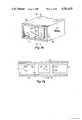
- FIG. 12aillustrates an assembled view of a millimeter-wave bandpass filter 1200 in accordance with the invention
- FIG. 12billustrates the bandpass filter of FIG. 12a in exploded form
- FIG. 12cillustrates the filter of FIGS. 12a and 12b viewed along the axis of the waveguide.
- Filter 1200includes mating conductive blocks 1212 and 1214 which are milled so that when mated they define an elongated rectangular waveguide 1210. The mated halves are held together by screws, one of which is illustrated as 1290 in FIG. 12b.
- a pair of thin conductive septa 1256 and 1256'extend across the narrow dimension of the rectangular waveguide in block 1212 and are spaced apart to define a fenestration 1254.
- a tuning arrangementis associated with block 1214.
- the tuning arrangementincludes a dielectric plate 1258 adhesively fastened to a brass screw 1260 threaded through a serrated nut 1262 captivated by a bracket 1254. As with the arrangement of FIGS. 2, 3 and 4, the tuning arrangement illustrated in FIGS.
- the waveguidehas interior dimensions of 0.112 inches (2.84 mm) high and 0.224 inches (5.69 mm) wide.
- the conductive septaeach have a thickness of 0.005 inches (0.127 mm) and strip width in the direction of propagation of signal of 0.007 inches (1.96 mm).
- the aperture size defined by the spacing between septais 0.110 inches (2.79 mm).
- the dielectric sheet 1258has an overall length of 0.265 inches (6.73 mm) and a thickness of 0.005 inches (0.127 mm).
- FIG. 13aillustrates the transmission characteristics of filter 1200.
- the maximum transmissionoccurs at approximately 44 GHz, and the through loss is approximately 1 dB.
- FIG. 13billustrates the return loss for the same tuning condition as that of FIG. 13a. As illustrated, maximum return loss (representing best impedance match) is approximately 15 dB at 44 GHz.
- FIG. 14aillustrates through loss for other positions of dielectric tuning plate 1258 as adjusted by serrated nut 1262.
- Plot 1410is a plot of through loss showing maximum transmission at about 41.5 GHz
- plot 1450illustrates a maximum transmission at about 40.5 GHz under a different tuning condition.
- FIG. 14billustrates as plot 1412 the return loss of the waveguide filter with the tuning which gave transmission plot 1410, and also illustrates as plot 1452 the return loss associated with the tuning of the filter which gave the through loss of plot 1450.
- FIG. 15aillustrates in cut away isometric view a bandpass filter including step transitions in the waveguide dimensions for reducing higher order mode interaction between resonators to improve the stop-band attenuation and to reduce spurious pass-band response.
- the bandpass filter characteristicis desired at a frequency which is near the lower end of the pass-band characteristic of the smaller waveguide, which is defined by conductive broad walls 1540' and 1542' spaced apart by narrow conductive walls 1544' and 1546'.
- a step transitionis made at a location 1590 to a larger size waveguide defined by broad walls 1540 and 1542 spaced apart by narrow walls 1544 and 1546.
- a conductive septum within the larger waveguide sectiondefines upper and lower ridges R and R' respectively, and conductive interconnections 1556, 1556' and 1556".
- the upper and lower ridges R, R' together with interconnections 1556, 1556' and 1556"define a pair of fenestrations 1554, 1554'.
- a further step transitionis made at a location 1590' from a larger dimension back to smaller dimensions waveguide defined by walls 1540", 1542", 1544"and 1546".
- the filtermay be formed within an undersized portion of waveguide, as illustrated in the cut away view of FIG. 16.
- a step transitionoccurs at locations 1690 between a waveguide defined by broad walls 1640', 1642' and narrow walls 1644' and 1646' and an undersize portion defined by broad walls 1640, 1642 and narrow walls 1644 and 1646.
- the undersize portion of waveguidealso includes spaced-apart conductive septa such as 1656, 1656' and 1656", which coact to define a bandpass characteristic.
- a dielectric tuning plate 1658which is attached to a plunger 1660 extending through an aperture 1695 in narrow wall 1646 to provide for motion of dielectric plate 1658.
- a further step transitionoccurs at a location 1690' from the undersize waveguide back to a larger waveguide defined by broad walls 1640", 1642” and narrow walls 1644", 1646".
- FIG. 17illustrates a circular waveguide including a tubular outer wall 1740.
- a conductive septum 1756includes ridge portions R and R' and apertures, one of which is designated 1754.
- a dielectric plate 1758is curved to conform to the general curvature of the electric fields in the circular waveguide, although this is not absolutely necessary.
- a shaft or actuating rod 1760 affixed to dielectric element 1758allows movement of the dielectric plate in a direction orthogonal to that of septum 1756 for tuning the filter.
- FIG. 18illustrates a cross-sectional view similar to that of FIGS. 3 and 5, in which a conductive sheet 1822 bonded to a broad surface of a dielectric plate 1818 defines ridges R, R', conductive interconnections, one of which is illustrated as 1856", and fenestration (not designated), and in which conductive sheet 1822 is centered on longitudinal axis 1802 midway between the inner surfaces of conductive narrow walls 1844 and 1846.
Landscapes
- Physics & Mathematics (AREA)
- Electromagnetism (AREA)
- Control Of Motors That Do Not Use Commutators (AREA)
Abstract
Description
Claims (20)
Priority Applications (1)
| Application Number | Priority Date | Filing Date | Title |
|---|---|---|---|
| US06/876,487US4761625A (en) | 1986-06-20 | 1986-06-20 | Tunable waveguide bandpass filter |
Applications Claiming Priority (1)
| Application Number | Priority Date | Filing Date | Title |
|---|---|---|---|
| US06/876,487US4761625A (en) | 1986-06-20 | 1986-06-20 | Tunable waveguide bandpass filter |
Publications (1)
| Publication Number | Publication Date |
|---|---|
| US4761625Atrue US4761625A (en) | 1988-08-02 |
Family
ID=25367828
Family Applications (1)
| Application Number | Title | Priority Date | Filing Date |
|---|---|---|---|
| US06/876,487Expired - Fee RelatedUS4761625A (en) | 1986-06-20 | 1986-06-20 | Tunable waveguide bandpass filter |
Country Status (1)
| Country | Link |
|---|---|
| US (1) | US4761625A (en) |
Cited By (37)
| Publication number | Priority date | Publication date | Assignee | Title |
|---|---|---|---|---|
| US5138255A (en)* | 1989-03-20 | 1992-08-11 | Semitex Co., Ltd. | Method and apparatus for measuring lifetime of semiconductor material including waveguide tuning means |
| US5243309A (en)* | 1992-06-04 | 1993-09-07 | Ghz Technologies Inc. | Temperature stable folded waveguide filter of reduced length |
| US5515460A (en)* | 1994-12-22 | 1996-05-07 | At&T Corp. | Tunable silicon based optical router |
| GB2312100A (en)* | 1996-03-29 | 1997-10-15 | Samsung Electronics Co Ltd | Method for designing E-plane bandpass filter with conductive strip |
| US5777534A (en)* | 1996-11-27 | 1998-07-07 | L-3 Communications Narda Microwave West | Inductor ring for providing tuning and coupling in a microwave dielectric resonator filter |
| US5781085A (en)* | 1996-11-27 | 1998-07-14 | L-3 Communications Narda Microwave West | Polarity reversal network |
| US5808528A (en)* | 1996-09-05 | 1998-09-15 | Digital Microwave Corporation | Broad-band tunable waveguide filter using etched septum discontinuities |
| US6392508B1 (en)* | 2000-03-28 | 2002-05-21 | Nortel Networks Limited | Tuneable waveguide filter and method of design thereof |
| US6573810B2 (en)* | 2000-08-10 | 2003-06-03 | Alcatel | Device for transmitting electromagnetic signals across a structure including modules organized for two-for-one redundancy |
| FR2836286A1 (en)* | 2002-02-19 | 2003-08-22 | Commw Scient Ind Res Org | Low cost dielectric tuning method for E plane filter |
| EP1278265A3 (en)* | 2001-07-17 | 2004-01-07 | Netro Corporation | Highly integrated planar stacked millimeter wave transceiver |
| US6683513B2 (en) | 2000-10-26 | 2004-01-27 | Paratek Microwave, Inc. | Electronically tunable RF diplexers tuned by tunable capacitors |
| US6724280B2 (en)* | 2001-03-27 | 2004-04-20 | Paratek Microwave, Inc. | Tunable RF devices with metallized non-metallic bodies |
| US20060044082A1 (en)* | 2003-01-06 | 2006-03-02 | Dominique Lo Hine Tong | Waveguide e-plane rf bandpass filter with pseudo-elliptic response |
| US7288944B1 (en)* | 2005-07-11 | 2007-10-30 | The United States Of America As Represented By The Secretary Of The Navy | Evanescent waveguide apparatus and method for measurement of dielectric constant |
| WO2009157494A1 (en)* | 2008-06-23 | 2009-12-30 | 日本電気株式会社 | Waveguide filter |
| US20100232636A1 (en)* | 2009-03-11 | 2010-09-16 | You-Ruei Lin | Headset |
| US20110001583A1 (en)* | 2009-07-01 | 2011-01-06 | Spx Corporation | Filter apparatus and method |
| JP2011009806A (en)* | 2009-06-23 | 2011-01-13 | Nec Engineering Ltd | Tunable band pass filter |
| FR2954596A1 (en)* | 2009-12-22 | 2011-06-24 | Thales Sa | MICRO-WAVE FILTER PASS BAND TUNABLE IN FREQUENCY |
| CN103178357A (en)* | 2011-12-21 | 2013-06-26 | 索尼公司 | Microwave antenna and antenna element |
| WO2013187139A1 (en)* | 2012-06-12 | 2013-12-19 | 日本電気株式会社 | Bandpass filter for which bandpass frequency can be easily changed |
| US20150188208A1 (en)* | 2013-12-26 | 2015-07-02 | Institute Of Physics, Chinese Academy Of Sciences | Band-pass filter |
| CN105280998A (en)* | 2014-06-30 | 2016-01-27 | 日本电产科宝株式会社 | Tunable filter |
| CN105280999A (en)* | 2014-06-30 | 2016-01-27 | 日本电产科宝株式会社 | Tunable filter |
| WO2016095165A1 (en)* | 2014-12-18 | 2016-06-23 | 华为技术有限公司 | Tunable filter |
| WO2018012368A1 (en)* | 2016-07-13 | 2018-01-18 | 日本電気株式会社 | Waveguide filter |
| US20180034125A1 (en)* | 2015-03-01 | 2018-02-01 | Telefonaktiebolaget Lm Ericsson (Publ) | Waveguide E-Plane Filter |
| DE102017100714A1 (en) | 2017-01-16 | 2018-07-19 | Tesat-Spacecom Gmbh & Co. Kg | Frequency adjustable channel filter |
| US20180301781A1 (en)* | 2015-12-24 | 2018-10-18 | Huawei Technologies Co., Ltd. | Filter and wireless network device |
| WO2019017085A1 (en)* | 2017-07-20 | 2019-01-24 | 日本電気株式会社 | Tunable bandpass filter and configuration method therefor |
| US20190036190A1 (en)* | 2017-07-25 | 2019-01-31 | Zte Corporation | Tunable waveguide filters |
| RU2696817C1 (en)* | 2019-01-09 | 2019-08-06 | Михаил Борисович Гойхман | Tunable band-close waveguide filter |
| WO2019187761A1 (en)* | 2018-03-29 | 2019-10-03 | 日本電気株式会社 | Tunable band-pass filter and method of controlling same |
| EP3553878A4 (en)* | 2016-12-30 | 2019-10-16 | Huawei Technologies Co., Ltd. | VARIABLE TUNING FILTER AND VARIABLE-TUNING FILTER DEVICE |
| US11189896B2 (en) | 2017-12-21 | 2021-11-30 | Gowrish Basavarajappa | Tunable bandpass filter with constant absolute bandwidth using single tuning element |
| US11881607B1 (en)* | 2021-10-05 | 2024-01-23 | Lockheed Martin Corporation | Longitudinally ridged septum orthomode transducer polarizer |
Citations (7)
| Publication number | Priority date | Publication date | Assignee | Title |
|---|---|---|---|---|
| US2697209A (en)* | 1951-07-13 | 1954-12-14 | Itt | Tunable band pass filter |
| US3212034A (en)* | 1962-03-22 | 1965-10-12 | Trw Inc | Electromagnetic wave energy filtering |
| US3621483A (en)* | 1966-06-10 | 1971-11-16 | Int Standard Electric Corp | Waveguide filter |
| US3758879A (en)* | 1971-08-31 | 1973-09-11 | Int Standard Electric Corp | Variable directional coupler |
| US3940721A (en)* | 1974-05-09 | 1976-02-24 | Nippon Electric Company, Ltd. | Cavity resonator having a variable resonant frequency |
| US4135133A (en)* | 1977-03-14 | 1979-01-16 | Rca Corporation | Dual mode filter |
| US4320367A (en)* | 1979-03-29 | 1982-03-16 | Compagnie Industrielle Des Telecommunications Cit-Alcatel | Hyperfrequency filter |
- 1986
- 1986-06-20USUS06/876,487patent/US4761625A/ennot_activeExpired - Fee Related
Patent Citations (7)
| Publication number | Priority date | Publication date | Assignee | Title |
|---|---|---|---|---|
| US2697209A (en)* | 1951-07-13 | 1954-12-14 | Itt | Tunable band pass filter |
| US3212034A (en)* | 1962-03-22 | 1965-10-12 | Trw Inc | Electromagnetic wave energy filtering |
| US3621483A (en)* | 1966-06-10 | 1971-11-16 | Int Standard Electric Corp | Waveguide filter |
| US3758879A (en)* | 1971-08-31 | 1973-09-11 | Int Standard Electric Corp | Variable directional coupler |
| US3940721A (en)* | 1974-05-09 | 1976-02-24 | Nippon Electric Company, Ltd. | Cavity resonator having a variable resonant frequency |
| US4135133A (en)* | 1977-03-14 | 1979-01-16 | Rca Corporation | Dual mode filter |
| US4320367A (en)* | 1979-03-29 | 1982-03-16 | Compagnie Industrielle Des Telecommunications Cit-Alcatel | Hyperfrequency filter |
Non-Patent Citations (8)
| Title |
|---|
| Article entitled "A New Class of Optimized Fin-Line & E-Plane Metal Insert Filters with Improved Characteristics" by Vahldieck et al., published at pp. 182-184 of the 1985 IEEE MTT-S Digest. |
| Article entitled "Design of Waveguide E-Plane Filters with All-Metal Inserts" by Shih, published at pp. 695-704 of IEEE Transactions on Microwave Theory and Techniques, Jul. 1984. |
| Article entitled "Theory & Design of Low-Insertion Loss Fin-Line Filters" by Arndt et al., published at pp. 155-163 of IEEE Transactions on Microwave Theory and Techniques, Feb. 1982. |
| Article entitled A New Class of Optimized Fin Line & E Plane Metal Insert Filters with Improved Characteristics by Vahldieck et al., published at pp. 182 184 of the 1985 IEEE MTT S Digest.* |
| Article entitled Design of Waveguide E Plane Filters with All Metal Inserts by Shih, published at pp. 695 704 of IEEE Transactions on Microwave Theory and Techniques, Jul. 1984.* |
| Article entitled Theory & Design of Low Insertion Loss Fin Line Filters by Arndt et al., published at pp. 155 163 of IEEE Transactions on Microwave Theory and Techniques, Feb. 1982.* |
| The characteristics of various obstacles in waveguides are described in Chapter 9, pp. 142 157 of Microwave Transmission Design Data , by Moreno, republished 1958 by Dover.* |
| The characteristics of various obstacles in waveguides are described in Chapter 9, pp. 142-157 of "Microwave Transmission Design Data", by Moreno, republished 1958 by Dover. |
Cited By (73)
| Publication number | Priority date | Publication date | Assignee | Title |
|---|---|---|---|---|
| US5138255A (en)* | 1989-03-20 | 1992-08-11 | Semitex Co., Ltd. | Method and apparatus for measuring lifetime of semiconductor material including waveguide tuning means |
| US5243309A (en)* | 1992-06-04 | 1993-09-07 | Ghz Technologies Inc. | Temperature stable folded waveguide filter of reduced length |
| US5515460A (en)* | 1994-12-22 | 1996-05-07 | At&T Corp. | Tunable silicon based optical router |
| GB2312100A (en)* | 1996-03-29 | 1997-10-15 | Samsung Electronics Co Ltd | Method for designing E-plane bandpass filter with conductive strip |
| GB2312100B (en)* | 1996-03-29 | 1998-06-03 | Samsung Electronics Co Ltd | Method for designing E-Plane bandpass filter with conductive strip |
| US5808528A (en)* | 1996-09-05 | 1998-09-15 | Digital Microwave Corporation | Broad-band tunable waveguide filter using etched septum discontinuities |
| US5781085A (en)* | 1996-11-27 | 1998-07-14 | L-3 Communications Narda Microwave West | Polarity reversal network |
| US5777534A (en)* | 1996-11-27 | 1998-07-07 | L-3 Communications Narda Microwave West | Inductor ring for providing tuning and coupling in a microwave dielectric resonator filter |
| US6392508B1 (en)* | 2000-03-28 | 2002-05-21 | Nortel Networks Limited | Tuneable waveguide filter and method of design thereof |
| US6573810B2 (en)* | 2000-08-10 | 2003-06-03 | Alcatel | Device for transmitting electromagnetic signals across a structure including modules organized for two-for-one redundancy |
| US6683513B2 (en) | 2000-10-26 | 2004-01-27 | Paratek Microwave, Inc. | Electronically tunable RF diplexers tuned by tunable capacitors |
| US6724280B2 (en)* | 2001-03-27 | 2004-04-20 | Paratek Microwave, Inc. | Tunable RF devices with metallized non-metallic bodies |
| EP1278265A3 (en)* | 2001-07-17 | 2004-01-07 | Netro Corporation | Highly integrated planar stacked millimeter wave transceiver |
| FR2836286A1 (en)* | 2002-02-19 | 2003-08-22 | Commw Scient Ind Res Org | Low cost dielectric tuning method for E plane filter |
| NL1022722C2 (en)* | 2002-02-19 | 2003-11-11 | Commw Scient Ind Res Org | Low cost dielectric tuning method for E plane filter |
| US20040017272A1 (en)* | 2002-02-19 | 2004-01-29 | Smith Stephanie L. | Low cost dielectric tuning for E-plane filters |
| GB2387718A (en)* | 2002-02-19 | 2003-10-22 | Commw Scient Ind Res Org | E-plane filter including dielectric tuning |
| GB2387718B (en)* | 2002-02-19 | 2005-12-28 | Commw Scient Ind Res Org | Low cost dielectric tuning for e-plane filters |
| US20060044082A1 (en)* | 2003-01-06 | 2006-03-02 | Dominique Lo Hine Tong | Waveguide e-plane rf bandpass filter with pseudo-elliptic response |
| US7292123B2 (en)* | 2003-01-06 | 2007-11-06 | Thomson Licensing | Waveguide E-plane RF bandpass filter with pseudo-elliptic response |
| US7288944B1 (en)* | 2005-07-11 | 2007-10-30 | The United States Of America As Represented By The Secretary Of The Navy | Evanescent waveguide apparatus and method for measurement of dielectric constant |
| US8928433B2 (en) | 2008-06-23 | 2015-01-06 | Nec Corporation | Waveguide filter |
| WO2009157494A1 (en)* | 2008-06-23 | 2009-12-30 | 日本電気株式会社 | Waveguide filter |
| JP5392505B2 (en)* | 2008-06-23 | 2014-01-22 | 日本電気株式会社 | Waveguide filter |
| US20110084783A1 (en)* | 2008-06-23 | 2011-04-14 | Taketoshi Jinnai | Waveguide filter |
| US8311258B2 (en)* | 2009-03-11 | 2012-11-13 | Cheng Uei Precision Industry Co., Ltd. | Headset |
| US20100232636A1 (en)* | 2009-03-11 | 2010-09-16 | You-Ruei Lin | Headset |
| EP2448060A4 (en)* | 2009-06-23 | 2012-11-14 | Nec Corp | TUNING BAND FILTER |
| CN102804484A (en)* | 2009-06-23 | 2012-11-28 | 日本电气株式会社 | Tunable Band-pass Filter |
| JP2011009806A (en)* | 2009-06-23 | 2011-01-13 | Nec Engineering Ltd | Tunable band pass filter |
| US8878635B2 (en) | 2009-06-23 | 2014-11-04 | Nec Corporation | Tunable band-pass filter |
| US8063723B2 (en)* | 2009-07-01 | 2011-11-22 | Spx Corporation | Filter apparatus and method |
| US20110001583A1 (en)* | 2009-07-01 | 2011-01-06 | Spx Corporation | Filter apparatus and method |
| WO2011076698A1 (en)* | 2009-12-22 | 2011-06-30 | Thales | Frequency-tunable microwave bandpass filter |
| US8975985B2 (en) | 2009-12-22 | 2015-03-10 | Thales | Frequency-tunable microwave bandpass filter |
| FR2954596A1 (en)* | 2009-12-22 | 2011-06-24 | Thales Sa | MICRO-WAVE FILTER PASS BAND TUNABLE IN FREQUENCY |
| CN103178357A (en)* | 2011-12-21 | 2013-06-26 | 索尼公司 | Microwave antenna and antenna element |
| US20130234904A1 (en)* | 2011-12-21 | 2013-09-12 | Sony Corporation | Microwave antenna and antenna element |
| US9099787B2 (en)* | 2011-12-21 | 2015-08-04 | Sony Corporation | Microwave antenna including an antenna array including a plurality of antenna elements |
| WO2013187139A1 (en)* | 2012-06-12 | 2013-12-19 | 日本電気株式会社 | Bandpass filter for which bandpass frequency can be easily changed |
| CN104335413A (en)* | 2012-06-12 | 2015-02-04 | 日本电气株式会社 | Bandpass filter for which bandpass frequency can be easily changed |
| EP2860818A4 (en)* | 2012-06-12 | 2015-11-18 | Nec Corp | Bandpass filter for which bandpass frequency can be easily changed |
| US9590285B2 (en) | 2012-06-12 | 2017-03-07 | Nec Corporation | Waveguide bandpass filter having a ladder shape metal plate and which is tunable using a rotatable dielectric plate |
| CN104335413B (en)* | 2012-06-12 | 2016-06-29 | 日本电气株式会社 | The band filter of bandpass frequency can be easily varied |
| US20150188208A1 (en)* | 2013-12-26 | 2015-07-02 | Institute Of Physics, Chinese Academy Of Sciences | Band-pass filter |
| US9537195B2 (en)* | 2013-12-26 | 2017-01-03 | Institute Of Physics, Chinese Academy Of Sciences | Rectangular band-pass filter having recesses of less than one-quarter wavelength depth formed therein for fitting a dielectric insert with a superconductive film within the recesses |
| JP2016015554A (en)* | 2014-06-30 | 2016-01-28 | 日本電産コパル株式会社 | Tunable filter |
| CN105280998B (en)* | 2014-06-30 | 2019-05-14 | 日本电产科宝株式会社 | Tunable optic filter |
| JP2016015555A (en)* | 2014-06-30 | 2016-01-28 | 日本電産コパル株式会社 | Tunable filter |
| CN105280999A (en)* | 2014-06-30 | 2016-01-27 | 日本电产科宝株式会社 | Tunable filter |
| CN105280998A (en)* | 2014-06-30 | 2016-01-27 | 日本电产科宝株式会社 | Tunable filter |
| CN105280999B (en)* | 2014-06-30 | 2019-05-14 | 日本电产科宝株式会社 | Tunable optic filter |
| CN106663853B (en)* | 2014-12-18 | 2019-11-29 | 华为技术有限公司 | Tunable filter |
| CN106663853A (en)* | 2014-12-18 | 2017-05-10 | 华为技术有限公司 | Tunable filter |
| WO2016095165A1 (en)* | 2014-12-18 | 2016-06-23 | 华为技术有限公司 | Tunable filter |
| US10333189B2 (en) | 2014-12-18 | 2019-06-25 | Huawei Technologies Co., Ltd. | Tunable filter |
| US9899716B1 (en)* | 2015-03-01 | 2018-02-20 | Telefonaktiebolaget Lm Ericsson (Publ) | Waveguide E-plane filter |
| US20180034125A1 (en)* | 2015-03-01 | 2018-02-01 | Telefonaktiebolaget Lm Ericsson (Publ) | Waveguide E-Plane Filter |
| US20180301781A1 (en)* | 2015-12-24 | 2018-10-18 | Huawei Technologies Co., Ltd. | Filter and wireless network device |
| US10873119B2 (en)* | 2015-12-24 | 2020-12-22 | Huawei Technologies Co., Ltd. | Filter and wireless network device |
| WO2018012368A1 (en)* | 2016-07-13 | 2018-01-18 | 日本電気株式会社 | Waveguide filter |
| US10873118B2 (en) | 2016-12-30 | 2020-12-22 | Huawei Technologies Co., Ltd. | Tunable filter and tunable filtering device |
| EP3553878A4 (en)* | 2016-12-30 | 2019-10-16 | Huawei Technologies Co., Ltd. | VARIABLE TUNING FILTER AND VARIABLE-TUNING FILTER DEVICE |
| DE102017100714A1 (en) | 2017-01-16 | 2018-07-19 | Tesat-Spacecom Gmbh & Co. Kg | Frequency adjustable channel filter |
| US10686237B2 (en) | 2017-01-16 | 2020-06-16 | Tesat-Spacecom Gmbh & Co. Kg | Channel filter with adjustable frequency |
| WO2019017085A1 (en)* | 2017-07-20 | 2019-01-24 | 日本電気株式会社 | Tunable bandpass filter and configuration method therefor |
| US11139547B2 (en) | 2017-07-20 | 2021-10-05 | Nec Corporation | Tunable bandpass filter and method of forming the same |
| US20190036190A1 (en)* | 2017-07-25 | 2019-01-31 | Zte Corporation | Tunable waveguide filters |
| US11189896B2 (en) | 2017-12-21 | 2021-11-30 | Gowrish Basavarajappa | Tunable bandpass filter with constant absolute bandwidth using single tuning element |
| WO2019187761A1 (en)* | 2018-03-29 | 2019-10-03 | 日本電気株式会社 | Tunable band-pass filter and method of controlling same |
| US11152676B2 (en) | 2018-03-29 | 2021-10-19 | Nec Corporation | Tunable band-pass filter and control method therefor |
| RU2696817C1 (en)* | 2019-01-09 | 2019-08-06 | Михаил Борисович Гойхман | Tunable band-close waveguide filter |
| US11881607B1 (en)* | 2021-10-05 | 2024-01-23 | Lockheed Martin Corporation | Longitudinally ridged septum orthomode transducer polarizer |
Similar Documents
| Publication | Publication Date | Title |
|---|---|---|
| US4761625A (en) | Tunable waveguide bandpass filter | |
| KR100319814B1 (en) | Dielectric Resonator Device | |
| US4371853A (en) | Strip-line resonator and a band pass filter having the same | |
| US3605045A (en) | Wide-band strip line frequency-selective circuit | |
| CA1245310A (en) | Interdigital duplexer with notch resonators | |
| US5969584A (en) | Resonating structure providing notch and bandpass filtering | |
| GB2039419A (en) | High frequency filter | |
| US4990870A (en) | Waveguide bandpass filter having a non-contacting printed circuit filter assembly | |
| US4660004A (en) | Duplexer including integral interdigital transmitter and receiver filters and three-quarter wavelength antenna transformer section | |
| US6504456B2 (en) | Communication device having a spurious wave blocking circuit formed of a plural fundamental pattern | |
| US4783639A (en) | Wideband microwave diplexer including band pass and band stop resonators | |
| US4603311A (en) | Twin strip resonators and filters constructed from these resonators | |
| US6597260B2 (en) | Filter, multiplexer, and communication apparatus | |
| US20040246071A1 (en) | Radio-frequency filter, in particular in the form of a duplex filter | |
| US11682817B1 (en) | W-band E-plane waveguide bandpass filter | |
| JPH118501A (en) | Dielectric filter, transmitter receiver in common, and communications equipment | |
| JP3405198B2 (en) | Non-radiative dielectric line resonator, non-radiative dielectric line filter, duplexer using the same, and communication device | |
| EP0957527A2 (en) | A microwave diplexer arrangement | |
| IL124304A (en) | Integrated evanescent mode filter with adjustable attenuator | |
| US6359534B2 (en) | Microwave resonator | |
| JP4611811B2 (en) | Fin line type microwave band pass filter | |
| EP1143552A1 (en) | Sheet-metal filter | |
| CA2270295C (en) | Dielectric filter, transmission-reception sharing unit, and communication device | |
| Yoneyama et al. | Experimental design of millimeter‐wave nonradiative dielectric waveguide filters | |
| Majewski et al. | MIC Directional Filters Using Dielectric Resonators |
Legal Events
| Date | Code | Title | Description |
|---|---|---|---|
| AS | Assignment | Owner name:RCA CORPORATION, A CORP. OF DE. Free format text:ASSIGNMENT OF ASSIGNORS INTEREST.;ASSIGNOR:SHARMA, ARVIND K.;REEL/FRAME:004581/0013 Effective date:19860618 Owner name:RCA CORPORATION, A CORP. OF DE.,NEW JERSEY Free format text:ASSIGNMENT OF ASSIGNORS INTEREST;ASSIGNOR:SHARMA, ARVIND K.;REEL/FRAME:004581/0013 Effective date:19860618 | |
| FEPP | Fee payment procedure | Free format text:PAYOR NUMBER ASSIGNED (ORIGINAL EVENT CODE: ASPN); ENTITY STATUS OF PATENT OWNER: LARGE ENTITY | |
| AS | Assignment | Owner name:GENERAL ELECTRIC COMPANY Free format text:MERGER;ASSIGNOR:R C A CORPORATION, A CORP. OF DE.;REEL/FRAME:004837/0618 Effective date:19880129 Owner name:GENERAL ELECTRIC COMPANY,STATELESS Free format text:MERGER;ASSIGNOR:R C A CORPORATION, A CORP. OF DE.;REEL/FRAME:004837/0618 Effective date:19880129 | |
| REMI | Maintenance fee reminder mailed | ||
| LAPS | Lapse for failure to pay maintenance fees | ||
| FP | Lapsed due to failure to pay maintenance fee | Effective date:19920802 | |
| STCH | Information on status: patent discontinuation | Free format text:PATENT EXPIRED DUE TO NONPAYMENT OF MAINTENANCE FEES UNDER 37 CFR 1.362 |