US4761587A - Multiple frequency horizontal oscillator for video apparatus - Google Patents
Multiple frequency horizontal oscillator for video apparatusDownload PDFInfo
- Publication number
- US4761587A US4761587AUS06/942,894US94289486AUS4761587AUS 4761587 AUS4761587 AUS 4761587AUS 94289486 AUS94289486 AUS 94289486AUS 4761587 AUS4761587 AUS 4761587A
- Authority
- US
- United States
- Prior art keywords
- frequency
- output signal
- oscillator
- signal
- video information
- Prior art date
- Legal status (The legal status is an assumption and is not a legal conclusion. Google has not performed a legal analysis and makes no representation as to the accuracy of the status listed.)
- Expired - Lifetime
Links
Images

Classifications
- H—ELECTRICITY
- H04—ELECTRIC COMMUNICATION TECHNIQUE
- H04N—PICTORIAL COMMUNICATION, e.g. TELEVISION
- H04N3/00—Scanning details of television systems; Combination thereof with generation of supply voltages
- H04N3/10—Scanning details of television systems; Combination thereof with generation of supply voltages by means not exclusively optical-mechanical
- H04N3/16—Scanning details of television systems; Combination thereof with generation of supply voltages by means not exclusively optical-mechanical by deflecting electron beam in cathode-ray tube, e.g. scanning corrections
- H04N3/27—Circuits special to multi-standard receivers
Definitions
- This inventionrelates to video apparatus and, in particular, to video apparatus that operate at a number of different line rate frequencies.
- a video apparatussuch as a television receiver or a computer monitor, for example, receives video information at a particular rate or frequency.
- the deflection or scanning circuits of the video apparatusare synchronized to the frequency of the video information in order to display the video information on a cathode ray tube.
- the video informationoccurs at fixed, predetermined rates and methods of synchronization of the deflection systems are well known and relatively straightforward.
- a computer monitormay be designed to be compatible with a variety of different computers of different manufacturers, which may produce video signals at different information rates. The range of possible operating frequencies may also be quite large, further complicating the deflection system design.
- a video apparatusincorporates a deflection circuit capable of operating at a frequency determined by an incoming information rate signal.
- the deflection circuitincludes an oscillator that produces an output signal having a frequency determined by the level of an input signal.
- a circuitperiodically varies the level of the oscillator input signal to cause the oscillator to vary its output signal frequency.
- Circuitryproduces an output signal when the oscillator output signal frequency and the frequency of the incoming video information rate signal correspond. Circuitry responds to that output signal and maintains the oscillator output signal at the frequency of the incoming video information rate signal.
- FIG. 1is a block and schematic diagram of a portion of a video apparatus in accordance with an aspect of the present invention
- FIG. 2is a schematic diagram of an alternate embodiment of a portion of the circuit shown in FIG. 1;
- FIG. 3is a schematic diagram of an alternate embodiment of another portion of the circuit shown in FIG. 1.
- FIG. 1there is shown a portion of a video apparatus, illustrated as a color computer monitor, in which a video signal in the form of red, green and blue color video components are applied to the video display apparatus from an external source (not shown), such as a computer, via an input terminal strip 10.
- the color video componentsdesignated R, G, and B are applied to chrominance and luminance processing circuitry 11 which generates red, green and blue color drive signals.
- the color drive signalsare applied via a conductor 12 to the electron gun assembly 13 located within the neck of a cathode ray tube (CRT) 14.
- CTRcathode ray tube
- a composite synchronizing (sync) signaldesignated CS
- CScomposite synchronizing
- the sync signalis applied to deflection processing circuitry 15, where it is separated into the respective line and field rate sync information components or pulses.
- Deflection processing circuitry 15is illustratively shown as an integrated circuit designated TDA 2595, manufactured by Signetics Corporation. Device terminal numbers are also illustrated within the outline of deflection processing circuitry 15.
- the field rate, or vertical, sync pulsesare applied via a conductor designated VS to vertical deflection circuitry 16 which produces vertical or field rate deflection current via terminal V and V' in vertical deflection winding 17, located on CRT 14.
- the deflection current flowing in deflection winding 17creates an electromagnetic deflection field that provides vertical deflection of the electron beams 22 generated by electron gun assembly 13 in a predetermined pattern across phosphor display screen 23 located on the front panel of CRT 14.
- Proper operation of the deflection circuitsmay require adjustment of the operating supply voltages at different deflection or operating frequencies. This is illustratively accomplished in the following manner.
- a source of powersuch as AC line supply 24, is connected to a rectifying circuit 25 and a filter capacitor 26 to provide a source of unregulated DC voltage at a terminal 27.
- the unregulated DC voltageis applied to one terminal of a winding 30 of a power transformer 31.
- the other terminal of winding 30is connected to the collector of a switching transistor 32.
- Conduction of transistor 32determined by control circuit 33, causes current to flow in winding 30 which, by transformer action, causes current to flow in windings 34, 35 and 36.
- the current in winding 34is rectified by diode 37 and charges capacitor 40 to develop a feedback voltage that is applied to control circuit 33.
- control circuit 33controls the conduction interval of transistor 32 in order to maintain the voltage across capacitor 40 at a constant regulated level.
- Transformer 31also provides electrical isolation between the "hot” AC line and the "cold” load circuits and user interface connectors, such as input terminal strip 10.
- Winding 35 currentrectified by diode 41, charges capacitor 42 to provide a voltage at a terminal 43 that is used to power various circuits of the video display apparatus, such as chrominance and luminance processing circuit 11, for example.
- the voltage established across capacitor 44, derived from winding 36 via diode 45,is applied to the drain terminal of a field effect transistor (FET) 46, which forms part of a frequency dependent power supply circuit 47 that operates as follows.
- FETfield effect transistor
- Power supply circuit 47operating as a DC to DC converter, incorporates pulse width modulating circuit 50, which receives an input signal at a terminal 51 from deflection processing circuitry 15. This input signal comprises pulses occurring at the horizontal deflection or line rate, which are derived in accordance with an aspect of the present invention in a manner that will be described later.
- Pulse width modulator circuit 50illustratively comprises an integrated circuit designated NE5560, manufactured by Signetics Corporation. Pulse width modulator circuit 50 produces an output signal incorporating width-modulated pulses having a frequency determined in response to the input pulse frequency.
- the output signal of pulse width modulator circuit 50is applied via coupling capacitor 52 to primary winding 53 of a transformer 54.
- Secondary winding 55 of transformer 54has one terminal coupled via capacitor 56 to the cathode of a diode 57, the collector of a transistor 60, one terminal of a resistor 61 and the gate of FET 46.
- the other terminal of secondary winding 55is coupled to the anode of diode 57, a transistor bias resistor 62, the emitter of transistor 60, the cathode of a flywheel diode 59, the other terminal of resistor 61 and the source terminal of FET 46.
- the source terminal of FET 46is also coupled to a supply capacitor 63 via an inductor 64.
- Transformer 54provides DC isolation that allows the secondary circuits to be referenced to the voltage across capacitor 63.
- the voltage developed across tertiary winding 70forms a high voltage or ultor potential at a terminal 71 that is applied to CRT 14.
- the voltage developed across secondary winding 66is applied to deflection processing circuitry 15 via a terminal 68. This voltage also develops a DC voltage level via diode 58 and a capacitor 69 that provides power to pulse width modulator circuit 50.
- Pulses from pulse width modulator circuit 50are coupled from the primary winding of transformer 54 to the base of transistor 60 via differentiating network 72 comprising resistor 73, capacitor 74, and diode 75.
- the leading edge of the turn-off pulse for FET 46is differentiated by differentiating network 72 to form a positive going pulse signal which is applied to the base of transistor 60.
- the differentiated pulse from the trailing edge of the modulator 50 pulsesis reduced in amplitude by diode 75.
- the differentiated positive-going pulsesquickly turn on transistor 60 which in turn rapidly turn off FET 46.
- a video apparatusparticularly a video apparatus used as a computer monitor, be capable of operating at different video information rate frequencies in order to enhance the compatibility of the video apparatus when used with different computers.
- the video apparatus shown in FIG. 1will synchronize its operating frequency to that of any video information rate signal having a frequency occurring between predetermined upper and lower frequency limits, illustratively 15 KHz and 30 KHz, for example.
- Deflection processing circuitry 15produces output signal pulses at terminal 51, for example, having a pulse frequency determined by the level of the voltage applied to a terminal 80.
- Synchronization of the frequency of the output pulse signal at terminal 51 with the frequency of the incoming video information as represented by the horizontal deflection or line rate synchronizing signal component on conductor CSis provided as follows.
- Voltage sweep generator 81which may be of conventional design, produces a triangular output waveform that varies between a lower voltage level illustratively of the order of 1 volt and an upper voltage level illustratively of the order of 15 volts.
- the upper and lower voltage limitsare selected so that the voltage levels that are applied to terminal 80 of deflection processing circuitry 15 result in a frequency range that encompasses the desired line rate or frequency operating range of the video apparatus.
- the horizontal or line rate oscillator of deflection processing circuitry 15will in turn cyclically vary its operating frequency.
- the coincidence detector output of deflection processing circuitry 15 at terminal 82will be a defined low level signal.
- This low level outputapplied to the base of a transistor 83, will cause transistor 83 to be rendered nonconductive, which in turn maintains transistor 84 nonconductive.
- transistor 84 nonconductivethe voltage at the collector of transistor 84 is high so that field effect transistor (FET) 85 is rendered conductive.
- FET 85Conduction of FET 85 allows the output voltage of voltage sweep generator 81 to charge capacitor 90, so that the voltage across capacitor 90 will follow the output voltage of voltage sweep generator 81.
- Amplifier 91configured as a sample and hold circuit, acts to apply the voltage across capacitor 90 to input terminal 80 of deflection processing circuitry 15.
- the oscillator frequencywill at some time correspond to that of the incoming horizontal rate sync signal.
- the coincidence detector output at terminal 82will become a high level signal, thereby rendering transistor 83 conductive, which in turn causes transistor 84 to become conductive.
- the collector voltage of transistor 84will fall to a level sufficient to render FET 85 nonconductive.
- the voltage across capacitor 90will then no longer follow the varying output voltage of voltage sweep generator 81, but will instead be maintained at the voltage level required to provide an oscillator frequency corresponding to the incoming video information rate frequency.
- the input impedance of amplifier 91is very high so that the voltage level across capacitor 90 is maintained.
- the oscillator of the deflection processing circuitry 15is varied in a predetermined manner until coincidence with the incoming video information frequency is again established.
- the rate at which the output signal of voltage sweep generator 81 is varied between the frequency limitsillustratively of the order of 1 second, is selected to insure that any load circuit supply voltages that are required to be changed in response to the change in operating frequency have sufficient time to reach their desired voltage levels before the oscillator frequency is changed.
- the output pulses of deflection processing circuitry 15, which appear at terminal 51,are also applied to the base of a line rate driver transistor 92 and cause transistor 92 to switch conductive states at the line rate frequency. These switching pulses are transmitted via a driver transformer 93 to the base of a horizontal output transistor 94, which forms part of a resonant retrace type of deflection output circuit.
- the output circuitillustratively includes a damper diode 95, a retrace capacitor 96, a deflection winding 97, located on the neck of CRT 14 and connected via terminals H and H' and an S-shaping capacitor 100.
- the deflection output circuitcauses a horizontal or line rate deflection current to flow in deflection winding 97, which creates an electromagnetic deflection field that deflects or scans electron beam 22 across display screen 23 of CRT 14. Power is supplied to the output circuit via terminal 101 of winding 65. Retrace or flyback pulses produced by the switching of transistor 94 that appear across winding 65 result in the previously described voltages being developed across windings 66 and 70.
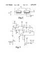
- FIG. 2illustrates the use of digital sampling components as an alternate embodiment.
- FIG. 2shows a digital sample and hold circuit 102 comprising an analog-to-digital converter 103, which samples the voltage across capacitor 90 and generates a corresponding digital value.
- a digital-to-analog converter 104transforms the digital value back into an analog value for application to deflection processing circuitry 15.
- a signal, illustratively provided from coincidence signal output terminal 82is applied to digital-to-analog converter 104 in order to maintain the digital value which corresponds to the desired oscillator input voltage.
- the advantage of digital circuit 102is that the storage of a digital value provides a more stable and accurate representation of the desired oscillator input voltage than is possible using analog techniques.
- FIG. 3illustrates an illustrative embodiment of a frequency to voltage converter that directly generates the desired oscillator input voltage in response to incoming video information frequency, thereby eliminating the need for a cyclically varying voltage signal.
- the frequency to voltage converteroperates as follows. Positive going line rate synchronizing pulses, indicative of the incoming video information rate, are provided by deflection processing circuitry 15 and applied to the base of transistor 105 via terminal 106. Immediately following the occurrence of a synchronizing pulse, transistor 105 is nonconductive, with its collector voltage at a defined high level. Capacitor 108 has discharged to a level such that the output level of comparator 107 is low and comparator 110 is high.
- Logic NAND gates 111 and 112are configured such that the output of NAND gate 112 is low, thereby rendering transistor 113 nonconductive.
- Capacitor 108begins to charge via a ramp generator essentially formed by transistors 114 and 115, diode 116, resistor 117 and capacitor 108. As capacitor 108 becomes charged, transistor 120 becomes conductive, thereby charging capacitor 121. Capacitor 108 continues to charge until the occurrence of a line rate synchronizing pulse renders transistor 105 conductive, bringing its collector voltage low, causing the output of comparator 110 to go low. The output of NAND gate 112 becomes high, rendering transistor 113 conductive and discharging capacitor 108. At the termination of the sync pulse, the cycle repeats.
- capacitor 121Over a number of line or horizontal intervals, capacitor 121 becomes charged to a level representative of the frequency of the incoming sync pulses.
- the voltage across capacitor 121may therefore be used to control the oscillator of deflection processing circuitry 15 in order to provide the desired oscillator frequency. If the incoming video information rate frequency should change, the charging interval of capacitor 108 will change, with the result that the conduction interval or duty cycle of transistor 120 also changes. Capacitor 121 therefore charges to a different voltage level indicative of the changed frequency.
Landscapes
- Engineering & Computer Science (AREA)
- Multimedia (AREA)
- Signal Processing (AREA)
- Details Of Television Scanning (AREA)
- Synchronizing For Television (AREA)
Abstract
Description
Claims (7)
Priority Applications (3)
| Application Number | Priority Date | Filing Date | Title |
|---|---|---|---|
| US06/942,894US4761587A (en) | 1986-12-17 | 1986-12-17 | Multiple frequency horizontal oscillator for video apparatus |
| JP62317247AJP2598053B2 (en) | 1986-12-17 | 1987-12-15 | Deflection circuit for video equipment |
| KR87014372AKR960009797B1 (en) | 1986-12-17 | 1987-12-17 | Deflection circuit |
Applications Claiming Priority (1)
| Application Number | Priority Date | Filing Date | Title |
|---|---|---|---|
| US06/942,894US4761587A (en) | 1986-12-17 | 1986-12-17 | Multiple frequency horizontal oscillator for video apparatus |
Publications (1)
| Publication Number | Publication Date |
|---|---|
| US4761587Atrue US4761587A (en) | 1988-08-02 |
Family
ID=25478780
Family Applications (1)
| Application Number | Title | Priority Date | Filing Date |
|---|---|---|---|
| US06/942,894Expired - LifetimeUS4761587A (en) | 1986-12-17 | 1986-12-17 | Multiple frequency horizontal oscillator for video apparatus |
Country Status (3)
| Country | Link |
|---|---|
| US (1) | US4761587A (en) |
| JP (1) | JP2598053B2 (en) |
| KR (1) | KR960009797B1 (en) |
Cited By (15)
| Publication number | Priority date | Publication date | Assignee | Title |
|---|---|---|---|---|
| WO1991019390A1 (en)* | 1990-06-01 | 1991-12-12 | Thomson Consumer Electronics, Inc. | Automatic letterbox detection |
| US5124671A (en)* | 1991-06-04 | 1992-06-23 | Zenith Electronics Corporation | Lock detector and confidence system for multiple frequency range oscillator control |
| US5136398A (en)* | 1989-08-23 | 1992-08-04 | Thomson Consumer Electronics, Inc. | Multiple display formats for letterbox signal |
| US5184091A (en)* | 1991-06-04 | 1993-02-02 | Zenith Electronics Corporation | Circuit for phase locking an oscillator within any one of a plurality of frequency ranges |
| US5249049A (en)* | 1990-06-01 | 1993-09-28 | Thomson Consumer Electronics, Inc. | Managing letterbox displays |
| US5266871A (en)* | 1991-01-07 | 1993-11-30 | Rca Thomson Licensing Corporation | High voltage stabilization circuit for video display apparatus |
| US5309234A (en)* | 1991-05-29 | 1994-05-03 | Thomson Consumer Electronics | Adaptive letterbox detector |
| US5337023A (en)* | 1993-06-01 | 1994-08-09 | National Semiconductor Corporation | Reduced phase-jitter horizontal sweep control phase-lock-loop and method |
| US5345270A (en)* | 1990-06-01 | 1994-09-06 | Thomson Consumer Electronics, Inc. | Managing letterbox signals with logos and closed captions |
| US5351135A (en)* | 1990-06-01 | 1994-09-27 | Thomson Consumer Electronics, Inc. | Managing letterbox signals with logos |
| US5434483A (en)* | 1993-10-19 | 1995-07-18 | Sampo Technology Corp. | Automatic compensation circuit for the horizontal deflection of a multifrequency computer monitor |
| US5486871A (en)* | 1990-06-01 | 1996-01-23 | Thomson Consumer Electronics, Inc. | Automatic letterbox detection |
| US6208093B1 (en)* | 1999-02-08 | 2001-03-27 | Thomson Licensing S.A. | Selectable clampers for an S-shaping voltage of a video display |
| US20050212976A1 (en)* | 2002-04-19 | 2005-09-29 | Snehali Choksi | Deflection supply voltage feedback control in conjunction with frequency change |
| US7142567B1 (en)* | 1999-04-01 | 2006-11-28 | Sedna Patent Services, Llc | Rate generator in a video on demand system having multiple constant bit rate data |
Citations (17)
| Publication number | Priority date | Publication date | Assignee | Title |
|---|---|---|---|---|
| US3127570A (en)* | 1959-11-18 | 1964-03-31 | Philips Corp | Circuit arrangement for synchronizing a local oscillator with the aid of a phase discriminator |
| US3593179A (en)* | 1968-10-31 | 1971-07-13 | Philips Corp | Phase discriminator for synchronizing a local oscillator |
| US3641258A (en)* | 1970-04-30 | 1972-02-08 | Rca Corp | Sample-and-hold circuit |
| US3946329A (en)* | 1974-06-05 | 1976-03-23 | The Magnavox Company | Electronic automatic frequency tuning system |
| US4253116A (en)* | 1979-11-27 | 1981-02-24 | Rca Corporation | Television synchronizing system operable from nonstandard signals |
| US4374437A (en)* | 1980-12-29 | 1983-02-15 | Zenith Radio Corporation | Variable ramp speed TV tuning system for rapid channel tuning |
| US4417279A (en)* | 1981-02-16 | 1983-11-22 | Hitachi, Ltd. | FM Television signal receiving circuit |
| US4439787A (en)* | 1981-02-18 | 1984-03-27 | Sony Corporation | AFT Circuit |
| US4443769A (en)* | 1981-04-27 | 1984-04-17 | Rca Corporation | Frequency search system for a phase locked loop |
| US4461999A (en)* | 1980-09-08 | 1984-07-24 | U.S. Philips Corporation | Circuit for producing a periodic sawtooth shaped signal |
| US4567447A (en)* | 1983-06-03 | 1986-01-28 | Zenith Electronics Corporation | Auto tuning for an oscillator |
| US4574224A (en)* | 1983-08-17 | 1986-03-04 | Zenith Electronics Corporation | Variable rate horizontal deflection system for a video monitor |
| US4598236A (en)* | 1983-12-22 | 1986-07-01 | Rockwell International Corporation | Background raster generator |
| US4612574A (en)* | 1983-10-14 | 1986-09-16 | Rca Corporation | Oscillator-frequency control interface circuit |
| US4634939A (en)* | 1985-12-24 | 1987-01-06 | Rca Corporation | Circuit synchronized by a signal at a deflection frequency |
| US4645989A (en)* | 1984-02-21 | 1987-02-24 | Rca Corporation | Frequency switching circuit for multiple scan rate video display apparatus |
| US4679091A (en)* | 1984-10-15 | 1987-07-07 | Sony Corporation | Multiple scanning type television receiver |
- 1986
- 1986-12-17USUS06/942,894patent/US4761587A/ennot_activeExpired - Lifetime
- 1987
- 1987-12-15JPJP62317247Apatent/JP2598053B2/ennot_activeExpired - Lifetime
- 1987-12-17KRKR87014372Apatent/KR960009797B1/ennot_activeExpired - Fee Related
Patent Citations (17)
| Publication number | Priority date | Publication date | Assignee | Title |
|---|---|---|---|---|
| US3127570A (en)* | 1959-11-18 | 1964-03-31 | Philips Corp | Circuit arrangement for synchronizing a local oscillator with the aid of a phase discriminator |
| US3593179A (en)* | 1968-10-31 | 1971-07-13 | Philips Corp | Phase discriminator for synchronizing a local oscillator |
| US3641258A (en)* | 1970-04-30 | 1972-02-08 | Rca Corp | Sample-and-hold circuit |
| US3946329A (en)* | 1974-06-05 | 1976-03-23 | The Magnavox Company | Electronic automatic frequency tuning system |
| US4253116A (en)* | 1979-11-27 | 1981-02-24 | Rca Corporation | Television synchronizing system operable from nonstandard signals |
| US4461999A (en)* | 1980-09-08 | 1984-07-24 | U.S. Philips Corporation | Circuit for producing a periodic sawtooth shaped signal |
| US4374437A (en)* | 1980-12-29 | 1983-02-15 | Zenith Radio Corporation | Variable ramp speed TV tuning system for rapid channel tuning |
| US4417279A (en)* | 1981-02-16 | 1983-11-22 | Hitachi, Ltd. | FM Television signal receiving circuit |
| US4439787A (en)* | 1981-02-18 | 1984-03-27 | Sony Corporation | AFT Circuit |
| US4443769A (en)* | 1981-04-27 | 1984-04-17 | Rca Corporation | Frequency search system for a phase locked loop |
| US4567447A (en)* | 1983-06-03 | 1986-01-28 | Zenith Electronics Corporation | Auto tuning for an oscillator |
| US4574224A (en)* | 1983-08-17 | 1986-03-04 | Zenith Electronics Corporation | Variable rate horizontal deflection system for a video monitor |
| US4612574A (en)* | 1983-10-14 | 1986-09-16 | Rca Corporation | Oscillator-frequency control interface circuit |
| US4598236A (en)* | 1983-12-22 | 1986-07-01 | Rockwell International Corporation | Background raster generator |
| US4645989A (en)* | 1984-02-21 | 1987-02-24 | Rca Corporation | Frequency switching circuit for multiple scan rate video display apparatus |
| US4679091A (en)* | 1984-10-15 | 1987-07-07 | Sony Corporation | Multiple scanning type television receiver |
| US4634939A (en)* | 1985-12-24 | 1987-01-06 | Rca Corporation | Circuit synchronized by a signal at a deflection frequency |
Cited By (18)
| Publication number | Priority date | Publication date | Assignee | Title |
|---|---|---|---|---|
| US5136398A (en)* | 1989-08-23 | 1992-08-04 | Thomson Consumer Electronics, Inc. | Multiple display formats for letterbox signal |
| US5345270A (en)* | 1990-06-01 | 1994-09-06 | Thomson Consumer Electronics, Inc. | Managing letterbox signals with logos and closed captions |
| US5351135A (en)* | 1990-06-01 | 1994-09-27 | Thomson Consumer Electronics, Inc. | Managing letterbox signals with logos |
| US5249049A (en)* | 1990-06-01 | 1993-09-28 | Thomson Consumer Electronics, Inc. | Managing letterbox displays |
| WO1991019390A1 (en)* | 1990-06-01 | 1991-12-12 | Thomson Consumer Electronics, Inc. | Automatic letterbox detection |
| US5486871A (en)* | 1990-06-01 | 1996-01-23 | Thomson Consumer Electronics, Inc. | Automatic letterbox detection |
| US5266871A (en)* | 1991-01-07 | 1993-11-30 | Rca Thomson Licensing Corporation | High voltage stabilization circuit for video display apparatus |
| US5309234A (en)* | 1991-05-29 | 1994-05-03 | Thomson Consumer Electronics | Adaptive letterbox detector |
| US5184091A (en)* | 1991-06-04 | 1993-02-02 | Zenith Electronics Corporation | Circuit for phase locking an oscillator within any one of a plurality of frequency ranges |
| US5124671A (en)* | 1991-06-04 | 1992-06-23 | Zenith Electronics Corporation | Lock detector and confidence system for multiple frequency range oscillator control |
| US5337023A (en)* | 1993-06-01 | 1994-08-09 | National Semiconductor Corporation | Reduced phase-jitter horizontal sweep control phase-lock-loop and method |
| US5434483A (en)* | 1993-10-19 | 1995-07-18 | Sampo Technology Corp. | Automatic compensation circuit for the horizontal deflection of a multifrequency computer monitor |
| US6208093B1 (en)* | 1999-02-08 | 2001-03-27 | Thomson Licensing S.A. | Selectable clampers for an S-shaping voltage of a video display |
| US7142567B1 (en)* | 1999-04-01 | 2006-11-28 | Sedna Patent Services, Llc | Rate generator in a video on demand system having multiple constant bit rate data |
| US20070091936A1 (en)* | 1999-04-01 | 2007-04-26 | Sedna Patent Services, Llc | Rate generator in a video on demand system having muliple constant bit rate data |
| US7567589B2 (en) | 1999-04-01 | 2009-07-28 | Comcast IP Holdings I, LLC. | Rate generator in a video on demand system having multiple constant bit rate data |
| US20050212976A1 (en)* | 2002-04-19 | 2005-09-29 | Snehali Choksi | Deflection supply voltage feedback control in conjunction with frequency change |
| US7030575B2 (en)* | 2002-04-19 | 2006-04-18 | Thomson Licensing | Deflection supply voltage feedback control in conjunction with frequency change |
Also Published As
| Publication number | Publication date |
|---|---|
| JPS63164766A (en) | 1988-07-08 |
| KR960009797B1 (en) | 1996-07-24 |
| KR880008622A (en) | 1988-08-31 |
| JP2598053B2 (en) | 1997-04-09 |
Similar Documents
| Publication | Publication Date | Title |
|---|---|---|
| US4761587A (en) | Multiple frequency horizontal oscillator for video apparatus | |
| CA1156356A (en) | Delay generator | |
| US4588929A (en) | Power supply and deflection circuit providing multiple scan rates | |
| CA1216667A (en) | Synchronized switching regulator for a multiple scanning frequency | |
| JPH021436B2 (en) | ||
| US5469029A (en) | Deflection apparatus for raster scanned CRT displays | |
| US4761586A (en) | Linearity correction for multiple frequency video apparatus | |
| EP0581154B1 (en) | Raster distortion correction circuit | |
| US4536684A (en) | Multiple scan rate deflection circuit incorporating scan compensation | |
| CA1167972A (en) | Raster distortion corrected deflection circuit | |
| US4985665A (en) | Black level tracking for multiple frequency apparatus | |
| US4510527A (en) | Horizontal deflection phasing arrangement | |
| US5218275A (en) | Beam landing location error correction arrangement | |
| US4731564A (en) | Service switch for video display apparatus | |
| US4234826A (en) | Synchronous switched vertical deflection driven during both trace and retrace intervals | |
| US4766390A (en) | CRT filament supply for multiple frequency video apparatus | |
| EP0844787B1 (en) | Dynamic focusing apparatus for cathode-ray tube display device | |
| US5466993A (en) | Deflection apparatus for raster scanned CRT displays | |
| CA1219358A (en) | Phase correction arrangement for deflection circuit | |
| US4740877A (en) | Power supply drive circuit improvement | |
| GB1595756A (en) | Set-up arrangement for a colour television receiver | |
| US5285133A (en) | Deflection current generating circuits | |
| US3201642A (en) | Augmented beta-boost voltage supply | |
| US4581630A (en) | Constant width burst gate keying pulse generator | |
| JP3840648B2 (en) | Video display device |
Legal Events
| Date | Code | Title | Description |
|---|---|---|---|
| AS | Assignment | Owner name:RCA CORPORATION, A CORP. OF DE. Free format text:ASSIGNMENT OF ASSIGNORS INTEREST.;ASSIGNOR:WHARTON, JAMES H.;REEL/FRAME:004650/0174 Effective date:19861216 Owner name:RCA CORPORATION Free format text:ASSIGNMENT OF ASSIGNORS INTEREST;ASSIGNOR:WHARTON, JAMES H.;REEL/FRAME:004650/0174 Effective date:19861216 | |
| AS | Assignment | Owner name:RCA LICENSING CORPORATION, TWO INDEPENDENCE WAY, P Free format text:ASSIGNMENT OF ASSIGNORS INTEREST.;ASSIGNOR:RCA CORPORATION, A CORP. OF DE;REEL/FRAME:004993/0131 Effective date:19871208 Owner name:RCA LICENSING CORPORATION, TWO INDEPENDENCE WAY, PRINCETON, NJ 08540, A CORP. OF DE Free format text:ASSIGNMENT OF ASSIGNORS INTEREST;ASSIGNOR:RCA CORPORATION, A CORP. OF DE;REEL/FRAME:004993/0131 Effective date:19871208 | |
| STCF | Information on status: patent grant | Free format text:PATENTED CASE | |
| FPAY | Fee payment | Year of fee payment:4 | |
| FPAY | Fee payment | Year of fee payment:8 | |
| FPAY | Fee payment | Year of fee payment:12 |