US4760607A - Apparatus and method for implementing transformations in grayscale image processing - Google Patents
Apparatus and method for implementing transformations in grayscale image processingDownload PDFInfo
- Publication number
- US4760607A US4760607AUS06/891,311US89131186AUS4760607AUS 4760607 AUS4760607 AUS 4760607AUS 89131186 AUS89131186 AUS 89131186AUS 4760607 AUS4760607 AUS 4760607A
- Authority
- US
- United States
- Prior art keywords
- signal
- word
- alu
- limit value
- enhanced
- Prior art date
- Legal status (The legal status is an assumption and is not a legal conclusion. Google has not performed a legal analysis and makes no representation as to the accuracy of the status listed.)
- Expired - Fee Related
Links
Images

Classifications
- G—PHYSICS
- G06—COMPUTING OR CALCULATING; COUNTING
- G06T—IMAGE DATA PROCESSING OR GENERATION, IN GENERAL
- G06T1/00—General purpose image data processing
- G06T1/20—Processor architectures; Processor configuration, e.g. pipelining
Definitions
- the present inventionrelates to image processing systems and methods, and more particularly to digital systems and methods for processing grayscale images.
- image processing systemshave been developed enabling digital computers to "see” or “read” an image.
- these image processorsinclude a video camera, an analog-to-digital converter for digitizing the video signal produced by the camera, and a digital system for processing the digitized information.
- the imagecan be digitized into a matrix, or lattice, of pixels with each of 512 video scan lines divided into 512 pixels.
- each pixelcan be encoded in a single bit, which is set to zero if the pixel is dark and set to one if the pixel is illuminated.
- each pixelis encoded in a multibit word which is set to a value corresponding to the illumination intensity of the pixel.
- Grayscale imagesare more realistic and detailed than nongrayscale images.
- the image processorsscan the digital images and process the digital information to interpret the image.
- the processorincludes a plurality of sequentially coupled logic units, each including a delay unit for delaying the serialized stream and a function unit for performing any one of a plurality of logical operations on the delayed and undelayed streams on a bit-by-bit basis.
- the Sternberg binary processoris capable of processing only bit-wide, or binary, data streams.
- the processorincludes one or more sequentially coupled logic units, each including a delay unit for delaying the serialized streams, an adder for adding a constant value to each word in the delayed stream, and a comparator unit for selecting the larger of the delayed and undelayed streams on a word-by-word basis.
- the processorhas two limitations. First, the operation of the logic units is not bounded. Consequently, manipulations of grayscale images occasionally produce data which exceeds the range of the processor's multibit format, producing virtual images which are difficult or even impossible to interpret. Second, the function unit is capable of selecting only a maximum value on a word-by-word basis between the delayed and undelayed streams. Consequently, the processor is capable of only dilation and erosion. The early Sternberg grayscale processor is therefore incapable of effecting many desired image transformations.
- Another image processorless efficient than the previously described Sternberg processors, routes a grayscale serial signal sequentially through several neighborhood transformations to detect limited image features. Disclosures of this processor are provided in U.S. Pat. No. 4,395,699, issued July 26, 1983, to Sternberg, entitled METHOD AND APPARATUS FOR PATTERN RECOGNITION AND DETECTION, and U.S. Pat. No. 4,322,716, issued Mar. 30, 1982, to Sternberg, entitled METHOD AND APPARATUS FOR PATTERN RECOGNITION AND DETECTION.
- the "neighborhood" of pixels surrounding a given pixel in one imageis examined and the corresponding pixel in the new image is given a value which is a function of the neighborhood pixels in the old image.
- All neighborhood pixels in an imageare made available for processing by serially routing the digital image through one or more fixed-length shift registers. As the image is shifted through the registers, the appropriate register locations are simultaneously accessed to process a particular neighborhood.
- This neighborhood processorhas drawbacks. First, the entire neighborhood of a pixel must be made available and examined before the corresponding pixel in the new image can be given a value. This requires excessively complicated circuitry to make the neighborhood pixels simultaneously available to drive the neighborhood function generator. Second, the neighborhood processing theory is an inefficient and cumbersome method of effecting many image transformations. Third, the neighborhood theory greatly restricts the operations which can be performed, due to the limited size or extent of the neighborhood.
- the image processorincludes a geometric logic unit (GLU) for receiving at least one input image and outputting at least one output image.
- GLUgeometric logic unit
- the GLUincludes at least one GLU stage, which each in turn include a delay element and a function unit.
- the function unitin turn includes an arithmetic logic unit (ALU) and an ALU controller.
- ALUarithmetic logic unit
- the function unit of the GLU stagethen operates on the undelayed and delayed serial streams on a word-by-word basis.
- a preselected constant valueis added to the delayed data to produce an "enhanced" data serial stream; and the ALU controller sets a first flag responsive to whether an overflow occurred during such addition.
- the enhanced datais subtracted from the undelayed data; and the ALU controller sets a second flag responsive whether underflow occurred during such subtraction.
- the output of the ALUis formed by selecting on a word-by-word basis (1) a limit value, (2) the undelayed data word, or (3) the enhanced data word depending upon whether overflow and/or underflow occurred during the addition and/or subtraction, respectively.
- the described function unitperforms rapidly, accurately, and efficiently.
- the function unit"clips" the output data to insure that data which overflows is not outputted in the output stream. Put another way, if the function unit results are too large to be represented in the multibit format, the function unit clips this information at the maximum value which can be represented in the format. This vastly improves the ease of image interpretation.
- the defined systemenables the GLU to be implemented using a conventional ALU and a specialized ALU controller. This reduces the cost of the system and increases the reliability of the system.
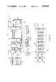
- FIG. 1is a schematic diagram showing the image processor of the present invention
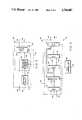
- FIG. 2is a schematic diagram of the geometric logic unit (GLU);
- FIG. 3is a schematic diagram of one stage of a GLU with the function unit illustrated conceptually;
- FIG. 4is a schematic diagram of the GLU stage function unit
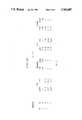
- FIG. 5is a flow chart illustrating the operation of the GLU stage function unit.
- FIG. 6is a logic table showing the output of the GLU stage function unit for various operations.
- a grayscale image processor 10 constructed in accordance with a preferred embodiment of the inventionis illustrated in FIG. 1, wherein data lines are illustrated as solid lines and control lines are indicated as broken lines.
- the processor 10includes a processing unit 12, a camera 14, a monitor 16, and a control computer 18.
- the camera 14provides real images to both the processing unit 12 and the monitor 16.
- the processing unit 12is capable of manipulating the real images inputted by the camera 14 to produce a variety of virtual images, or image transformations, useful in analyzing the real image.
- the monitor 16selectively displays either the real image observed by camera 14 or a virtual image produced by the processing unit 12.
- the control computer 18provides appropriate control signals to the various elements of the processing unit 12 to manipulate or transform the grayscale images according to an algorithm to produce a desired virtual image usable for feature extraction or other imaging information.
- the camera 14provides a standard EAI RS170 signal on an output line 20.
- This analog composite video signalis transmitted over line 20 at a rate of 30 frames per second with either 480 or 512 horizontal scan lines per frame.
- An analog/digital converter 22converts the analog serial signal received on the line 20 to a digital serial signal outputted on the bus 24 to the processing unit 12.
- the converter 22can convert a digital signal received on a bus 26 from the processing unit 12 to an analog signal on line 28 to be displayed on the monitor 16.
- the analog signal on the line 20 from the camera 14can be passed directly to the monitor 16 via the line 28.
- the digital signal on the eight-line bus 24includes one eight-bit word for each pixel in the video image.
- the analog signalis digitized into 512 pixels per line on each of the 480 or 512 scan lines. Therefore, the processed image is made up of a matrix or lattice of points or pixels.
- the eight-bit word corresponding to a pixelis given a value between zero and 255 inclusive depending on the intensity of the analog signal (light intensity) of the pixel. the value zero corresponds to total lack of intensity (i.e., darkness), while the value 255 corresponds to maximum intensity.
- the processing unit 12includes an arithmetic logic unit (ALU) 30, a geometric logic unit (GLU) 32, a count/locate unit (CLU) 34, and a frame buffer memory 36. All data buses interconnecting the elements of the processing unit 12 are at least eight bits wide enabling the grayscale serial signal to be transmitted over any one of the data buses.
- a pair of eight-bit buses 38 and 40interconnect the ALU and the GLU; a pair of eight-bit buses 42 and 44 interconnect the GLU 32 and the CLU 34; a 24-bit bus 46 interconnects the CLU 34 and the frame buffer 36; and 25 a 24-bit bus 48 interconnects the frame buffer 36 and each of the ALU 30 and the GLU 32.
- each serial signal streamis outputted on the bus 48 to either the ALU 30 or the GLU 32. If more than one serial stream is processed at a time, the serial streams are transmitted in parallel over the bus 48. From the ALU 30, the signals pass sequentially through the GLU 32 and the CLU 34 before returning to the frame buffer 36. From the GLU 32, the signals pass through the CLU 34 before returning to the frame buffer 36.
- the frame buffer memory 36is three 512-by-5l2-by-8-bit storage devices enabling three separate grayscale digital images to be stored simultaneously therein.
- the frame buffer 36is three Model FB512 storage devices manufactured by Imaging Technologies Incorporated of Wolburn, Mass. Under the control of the control computer 18, the content of any one or more of the images in the frame buffer 36 can be outputted onto the bus 48.
- the arithmetic logic unit (ALU) 30is a point or pixel processor, meaning that operations are carried out on the input image or images on a pixel-by-pixel basis to create one or two output images.
- the data bus 48conveys one or two digital images from the frame buffer 36 to the ALU 30 for processing.
- the digital image or images created by the ALU 30are outputted on either or both of the buses 38 and 40 to the GLU 32.
- the ALU 30is a Model ALU512 arithmetic logic unit manufactured by Imaging Technologies Incorporated of Wolburn, Mass.
- the ALU 30includes appropriate multiplexing at its front end to select the appropriate image or images from bus 48 to be processed by the ALU and outputted on either or both of the buses 38 and 40.
- the arithmetic functions which the ALU 30 is capable of performinginclude passing an image, adding two images, subtracting two images, multiplying two images, ANDing two images, ORing two images, or complementing an image.
- the geometric logic unit (GLU) 32is coupled to the ALU 30 by buses 38 and 40, to the CLU 34 by buses 42 and 44, and to the frame buffer 36 by bus 48.
- the GLU 32is more clearly illustrated in FIGS. 2-4 to be described below Suffice it to say at this point that the GLU 32 receives one or more serial digital signals from the ALU 30 and/or the frame buffer 36 for processing.
- the digital image or images created by the GLU 32are outputted on the buses 42 and 44 to the CLU 34.
- the count/locate unit (CLU) 34is connected by the buses 42 and 44 to the GLU 32 and by bus 46 to the frame buffer 36.
- One of two functionscan be performed by the CLU 34 as the serial signal stream passes therethrough.
- the CLU 34does not affect the values of the serial signal stream in either function.
- the CLU 34can output on the Multibus 50 the coordinates of pixels within a given grayscale range.
- the CLU 34can output on Multibus 50 a frequency count, or histogram, of pixels within a given grayscale range.
- the output coordinates and the histogram informationcan be utilized by computer 18 in further control of the processing unit 12.
- the digital image or images exiting the CLU 32 on the bus 46are identical to the image or images entering the CLU 32 on the buses 42 and 44.
- Control computer 18which is coupled to the converter 22, the ALU 30, the GLU 32, the CLU 34, and the frame buffer 36 through the Multibus 50.
- Control signalsare issued by the computer 18 over the Multibus 50 during each vertical retrace of the camera 14 to condition the processor 12 for a possible imaging operation during the next frame period of the camera.
- the serial signalis routed sequentially through either (1) the ALU 30, the GLU 32, and the CLU 34 or (2) the GLU 32 and the CLU 34 to return to the frame buffer 36.
- Each loop or processing pass through the processing unit 12can be performed once and only once during each frame period to produce one or more digital images to be stored in the frame buffer 26.
- Each frame or imagecontains approximately one-quarter million (250,000) pixels.
- the ALU 30, the GLU 32, and the CLU 34all operate at a speed of approximately 10 megahertz (MHz) to process one entire digital image during approximately one frame cycle and leave sufficient time for the control computer 18 to reprogram the processor 12 for operation during the next frame cycle.
- the computer 18comprises an INTEL 80286 microcomputer having a minimum of 512 kilobytes (K) of memory.
- Disk 52is conventionally coupled through bus 54 to the computer 18 to provide the requisite secondary storage for the computer.
- a terminal 56 including a keyboardis conventionally coupled through a bus 58 to the computer 18 to provide a means of communicating command signals to the control computer.
- the processing system 10 as thus far describedis somewhat similar to the image processing system disclosed in U.S. patent application Ser. No. 644,101, filed Aug. 24, 1984, by Sternberg, now U.S. Pat. No. 4,641,356, entitled APPARATUS AND METHOD FOR IMPLEMENTING DILATION AND EROSION TRANSFORMATIONS IN GRAYSCALE IMAGE PROCESSING.
- the disclosure of that applicationis specifically incorporated herein by reference.
- the present systemdiffers from the referenced system primarily in the construction of the GLU 32.
- the geometric logic unit 32is illustrated in greater detail in FIG. 2.
- the GLUincludes input MUXes 60 and a plurality of sequentially coupled stages 62.
- the MUXes 60are coupled to buses 38, 40, and 48 (see also FIG. 1).
- Two output buses 64 and 66couple the input MUXes 60 and the first stage 68.
- the input MUXes 60are capable of selecting any one of five input images for output on either of buses 64 and 66. In the preferred embodiment, two output images are always produced on the buses 64 and 66 for delivery to the stages 62.
- the control of the input MUXes 60is selected over the Multibus 50 by the control computer 18 (see also FIG. 1).
- the MUXes 60are implemented as look-up tables (LUTs).
- the GLU 32includes eight sequentially coupled stages 62 (FIG. 2).
- more than one GLUcan be sequentially inserted in the processor 12 to provide a multiple of eight stages (e.g., 16, 24, or 32). All GLUs would be coupled between the ALU 30 and the CLU 34.
- Each of the stages 62is generally identical with one another and includes two eight-bit input ports and two eight-bit output ports which feed the next stage.
- the output of the last stage 70serves as the output for buses 42 and 44 which in the preferred embodiment are coupled to the CLU 34.
- the buses 42 and 44are coupled to the next GLU (not shown).
- Each of the stages 62receives control signals over the Multibus 50 from the control computer 18 (see also FIG. 1) to configure the stages as will be described for an image processing pass.
- a geometric logic unit (GLU) stage 68(FIG. 3) corresponds to any one of the eight stages 62 illustrated in FIG. 2.
- the stage 68 illustrated in FIG. 3will be presumed to be the first stage.
- the stage 68includes a digital programmable variable delay 72 and a function unit assembly 74.
- the variable delay 72time delays the eight-bit signal received on bus 40 for subsequent utilization by the function unit assembly 74.
- the variable delaymay be implemented by shift registers or as the multibit logical extension of the binary delay disclosed in U.S. patent application Ser. No. 559,438, filed Dec. 8, 1983, by Sternberg et al, now U.S. Pat. No.
- the delay 72is dynamically programmable over the Multibus 50 by the control computer 18 (see also FIG. 1) to provide a delay in a given number of pixels (e.g., 511 pixels).
- the function unit assembly 74is illustrated conceptually in FIG. 3 and as actually implemented in FIG. 4.
- the function unit assembly 74includes an adder 76 and a logic unit 78.
- the adder 76receives the eight-bit serial stream over bus 75 and adds a constant value to each eight-bit word in the serial stream.
- the signal exiting the adder 76 on the eight-bit bus 80is referred to as the "enhanced" or "enhanced delayed" signal.
- the logic unit 78operates on the undelayed signal received over eight-bit bus 38 and the enhanced signal received over bus 80.
- the logic unitoutputs two eight-bit serial signals on the buses 82 and 84 for delivery to the next serially-coupled stage 62 which as described would be the second stage.
- the conceptual operation of the function unit assembly 74 as described in FIG. 3corresponds to that described in U.S. patent application Ser. No. 644,101, the early Sternberg grayscale processor.
- the function unit assembly 74includes a conventional eight-bit arithmetic logic unit (ALU) assembly 86 and an ALU controller 88.
- the ALU assembly 86should not be confused with the ALU 30 of FIG. 1.
- the ALU 30is a sophisticated ALU specifically adapted for image processing sold by Imaging Technologies Incorporated of Wolburn, Mass.
- the ALU 86 of FIG. 4is a conventional eight-bit ALU and in the preferred embodiment is that sold as Model AM29501 by Advanced Micro Devices, Inc. of Sunnyvale, Calif.
- the ALU 86includes an input multiplexer 90, registers 92, an ALU multiplexer 94, an ALU 96, and an output multiplexer 98.
- the input MUX 90receives three eight-bit inputs over buses 38, 75, and 100.
- the MUX 90is capable of delivering any one of the three inputs to any one of the registers 92 over bus 102.
- the registers 92are coupled to the ALU MUX 94 and the output of MUX 98 via bus 104.
- the ALU MUX 94is capable of selecting any one or two of the registers 92 for application to the ALU 96 over eight-bit buses 106 and 108.
- the ALU 96is capable of performing a wide variety of operations.
- the ALU 96is capable of addition, subtraction, ANDing, ORing, exclusive ORing, and complementing.
- the eight-bit output of the ALU 96is delivered to both the output MUX 98 and the input MUX 90 over bus 100.
- the output MUX 98receives as input all of the registers 92 and the ALU output bus 100.
- the output MUX 98is capable of selecting any one of the eight-bit words for output on the eight-bit buses 82 and 84.
- the ALU controller 88receives control signals over the Multibus 50 from the control computer 18 (see also FIG. 1) and in turn controls the input MUX 90, the registers 92, the ALU MUX 94, the ALU 96, and the output MUX 98.
- the implementation of the ALU controller 88 in view of this disclosurewould be well within the capabilities of one having ordinary skill in the art.
- the data received over bus 38is referred to as the fixed input data or F-IN.
- the data received over the bus 40is referred to as the delayed input data or D-IN.
- the output of the variable delay 72 on bus 75is referred to as the delayed data or D.
- the output of the adder 76is referred to as the enhanced data or E.
- the output on bus 82is referred to as the fixed output data or F-OUT.
- the data on output bus 84is referred to as the delayed output data or D-OUT.
- the operation of the function unit assembly 74is illustrated in the flow chart of FIG. 5.
- the ALU controller 88Before data is received over buses 38 and 75, the ALU controller 88 must be conditioned with certain information over Multibus 50.
- an E-value, a MAX-value, and zeroare stored in the ALU controller 88 prior to the reception of data on an imaging pass.
- the E-valueis a constant value to be added to each eight-bit word in the delayed value.
- the E-valuecorresponds to the constant utilized by the adder 76 (FIG. 3).
- the MAX-value in the preferred embodimentcorresponds to the largest value which can be stored in the eight-bit format. In the preferred embodiment, this is decimal 255 or hexadecimal FF.
- the value zerois utilized to prevent underflow which is simply a specialized version of overflow.
- the first data wordsare received over buses 38 and 75.
- the data on bus 38is referred to as F-IN while the data on bus 75 is referred to as D.
- the values F-IN and D received over buses 38 and 75are stored in registers 92.
- the processing for each pair of input words received on buses 38 and 75is illustrated in block 112.
- the enhanced data Eis produced by adding the D data and the E-value. This addition generates a carry designated C-1 indicating whether overflow occurred during the addition, exceeding the maximum value 255. In the preferred embodiment, C-1 is zero if overflow did not occur and C-1 is one if overflow did occur. Both the value E and the status or overflow flag C-1 are stored in registers 92.
- a "don't care" DC valueis generated by subtracting the F-IN value from the E value in the ALU 96. This subtraction generates a status or overflow flag C-2 which indicates whether F-IN is larger than E. In the preferred embodiment, if F-IN is smaller than E, C-2 is zero; while if F-IN is larger than E, C-2 is one. As a result of the subtraction, only the status flag C-2 is stored in the registers 92. After the addition and subtraction are performed, the output multiplexer 98 makes an output decision for both of buses 82 and 84 depending on the status flags C-1 and C-2. This output decision is illustrated in greater detail in FIG.
- the outputs on buses 82 and 84, F-OUT and D-OUT, respectively,are either E, F-IN, or the LIMIT value. If C-1 is one, indicating that overflow occurred during the enhancement addition, the limit value is outputted on both of buses 82 and 84 to "clip" the data at the maximum value. Clipping the data at the maximum value facilitates future processing and makes recovery much easier. If C-1 is zero indicating that overflow did not occur during the enhancement addition, all numbers are within range. In this case, the output decision is made based on the value C-2 which indicates whether E or F-IN is greater. The greater of the two values is outputted on both of buses 82 and 84 as F-OUT and D-OUT.
- the explode operation(FIG. 6) is generally identical to the clone operation just described with the exception that the F-IN data is always outputted as the F-OUT data.
- the D-OUT datais identical to that of the clone operation.
- the collapse operation(FIG. 6) is the converse of the clone operation. Whereas in a clone the enhancement value is added and then a maximum value selection is made, in the collapse operation the enhancement value is subtracted, and a minimum selection is made. If C-1 has the value one for any word pair during the collapse operation, a zero is outputted on both of buses 82 and 84 as F-OUT and D-OUT. This prevents underflow to maintain the numbers within range in the eight-bit format. If the C-1 value is zero, the output decision is made on the basis of C-2 to select the minimum of F-IN and E.
- the implode operation(FIG. 6) is identical to the collapse operation with the exception that the F-IN data is always outputted on bus 82 as the F-OUT data.
- the D-OUT datacorresponds identically to the collapse operation.
- truth table of FIG. 6implements the bounded unsigned situation, the method can be logically extended to unbounded and signed situations. All of these variations are intended to fall within the scope of the appended claims.
Landscapes
- Physics & Mathematics (AREA)
- General Physics & Mathematics (AREA)
- Engineering & Computer Science (AREA)
- Theoretical Computer Science (AREA)
- Image Processing (AREA)
- Facsimile Image Signal Circuits (AREA)
Abstract
Description
Claims (13)
Priority Applications (3)
| Application Number | Priority Date | Filing Date | Title |
|---|---|---|---|
| US06/891,311US4760607A (en) | 1986-07-31 | 1986-07-31 | Apparatus and method for implementing transformations in grayscale image processing |
| JP62192552AJPS6337481A (en) | 1986-07-31 | 1987-07-31 | Conversion apparatus and method for gray scale image processing |
| EP87306797AEP0255397A2 (en) | 1986-07-31 | 1987-07-31 | Grayscale image processing |
Applications Claiming Priority (1)
| Application Number | Priority Date | Filing Date | Title |
|---|---|---|---|
| US06/891,311US4760607A (en) | 1986-07-31 | 1986-07-31 | Apparatus and method for implementing transformations in grayscale image processing |
Publications (1)
| Publication Number | Publication Date |
|---|---|
| US4760607Atrue US4760607A (en) | 1988-07-26 |
Family
ID=25397960
Family Applications (1)
| Application Number | Title | Priority Date | Filing Date |
|---|---|---|---|
| US06/891,311Expired - Fee RelatedUS4760607A (en) | 1986-07-31 | 1986-07-31 | Apparatus and method for implementing transformations in grayscale image processing |
Country Status (3)
| Country | Link |
|---|---|
| US (1) | US4760607A (en) |
| EP (1) | EP0255397A2 (en) |
| JP (1) | JPS6337481A (en) |
Cited By (7)
| Publication number | Priority date | Publication date | Assignee | Title |
|---|---|---|---|---|
| US5003613A (en)* | 1988-12-21 | 1991-03-26 | Recognition Equipment Incorporated | Document processing system and method |
| WO1991011070A1 (en)* | 1990-01-05 | 1991-07-25 | Perry Scott M | Method and device for creating a facsimile of an image |
| US5436984A (en)* | 1991-05-14 | 1995-07-25 | Rautaruukki Oy | Minimum delay dilation/erosion filter |
| US6192160B1 (en)* | 1996-09-19 | 2001-02-20 | Hyundai Microelectronics Co., Ltd. | Hardware architectures for image dilation and erosion operations |
| US20050074140A1 (en)* | 2000-08-31 | 2005-04-07 | Grasso Donald P. | Sensor and imaging system |
| US7321699B2 (en) | 2002-09-06 | 2008-01-22 | Rytec Corporation | Signal intensity range transformation apparatus and method |
| US20100142855A1 (en)* | 2006-11-28 | 2010-06-10 | Commissariat A L'energie Atomique | Image processing system with morphological macro cell |
Citations (25)
| Publication number | Priority date | Publication date | Assignee | Title |
|---|---|---|---|---|
| US3761876A (en)* | 1971-07-28 | 1973-09-25 | Recognition Equipment Inc | Recognition unit for optical character reading system |
| US3805035A (en)* | 1970-06-10 | 1974-04-16 | Ass Rech Et Le Dev Des Methode | Device for the logical analysis of textures |
| US3959771A (en)* | 1972-10-13 | 1976-05-25 | Hitachi, Ltd. | Pattern recognition apparatus |
| US4122496A (en)* | 1977-02-23 | 1978-10-24 | International Business Machines Corporation | Apparatus and method for digital halftone reproduction |
| US4167728A (en)* | 1976-11-15 | 1979-09-11 | Environmental Research Institute Of Michigan | Automatic image processor |
| US4242662A (en)* | 1978-10-16 | 1980-12-30 | Nippon Telegraph And Telephone Public Corporation | Method and apparatus for pattern examination |
| US4288779A (en)* | 1978-07-08 | 1981-09-08 | Agency Of Industrial Science & Technology | Method and apparatus for character reading |
| US4290049A (en)* | 1979-09-10 | 1981-09-15 | Environmental Research Institute Of Michigan | Dynamic data correction generator for an image analyzer system |
| US4301443A (en)* | 1979-09-10 | 1981-11-17 | Environmental Research Institute Of Michigan | Bit enable circuitry for an image analyzer system |
| US4322716A (en)* | 1976-11-15 | 1982-03-30 | Environmental Research Institute Of Michigan | Method and apparatus for pattern recognition and detection |
| US4345312A (en)* | 1979-04-13 | 1982-08-17 | Hitachi, Ltd. | Method and device for inspecting the defect of a pattern represented on an article |
| US4395699A (en)* | 1979-09-10 | 1983-07-26 | Environmental Research Institute Of Michigan | Method and apparatus for pattern recognition and detection |
| US4395697A (en)* | 1980-08-15 | 1983-07-26 | Environmental Research Institute Of Michigan | Off-image detection circuit for an image analyzer |
| US4395700A (en)* | 1980-08-15 | 1983-07-26 | Environmental Research Institute Of Michigan | Image analyzer with variable line storage |
| US4395698A (en)* | 1980-08-15 | 1983-07-26 | Environmental Research Institute Of Michigan | Neighborhood transformation logic circuitry for an image analyzer system |
| US4398176A (en)* | 1980-08-15 | 1983-08-09 | Environmental Research Institute Of Michigan | Image analyzer with common data/instruction bus |
| US4414685A (en)* | 1979-09-10 | 1983-11-08 | Sternberg Stanley R | Method and apparatus for pattern recognition and detection |
| US4442543A (en)* | 1979-09-10 | 1984-04-10 | Environmental Research Institute | Bit enable circuitry for an image analyzer system |
| US4464788A (en)* | 1979-09-10 | 1984-08-07 | Environmental Research Institute Of Michigan | Dynamic data correction generator for an image analyzer system |
| US4484346A (en)* | 1980-08-15 | 1984-11-20 | Sternberg Stanley R | Neighborhood transformation logic circuitry for an image analyzer system |
| EP0132134A2 (en)* | 1983-07-13 | 1985-01-23 | Machine Vision International Corporation | Digital image processing |
| EP0145477A2 (en)* | 1983-12-08 | 1985-06-19 | Machine Vision International Corporation | Digital image processing |
| US4541114A (en)* | 1983-05-05 | 1985-09-10 | Research Environmental/Institute of Michigan | Routing techniques using serial neighborhood image analyzing system |
| EP0177160A2 (en)* | 1984-08-24 | 1986-04-09 | Machine Vision International Corporation | Apparatus and method for implementing dilation and erosion transformation in grayscale image processing |
| US4635292A (en)* | 1983-12-19 | 1987-01-06 | Matsushita Electric Industrial Co., Ltd. | Image processor |
- 1986
- 1986-07-31USUS06/891,311patent/US4760607A/ennot_activeExpired - Fee Related
- 1987
- 1987-07-31JPJP62192552Apatent/JPS6337481A/enactivePending
- 1987-07-31EPEP87306797Apatent/EP0255397A2/ennot_activeWithdrawn
Patent Citations (28)
| Publication number | Priority date | Publication date | Assignee | Title |
|---|---|---|---|---|
| US3805035A (en)* | 1970-06-10 | 1974-04-16 | Ass Rech Et Le Dev Des Methode | Device for the logical analysis of textures |
| US3761876A (en)* | 1971-07-28 | 1973-09-25 | Recognition Equipment Inc | Recognition unit for optical character reading system |
| US3959771A (en)* | 1972-10-13 | 1976-05-25 | Hitachi, Ltd. | Pattern recognition apparatus |
| US4322716A (en)* | 1976-11-15 | 1982-03-30 | Environmental Research Institute Of Michigan | Method and apparatus for pattern recognition and detection |
| US4167728A (en)* | 1976-11-15 | 1979-09-11 | Environmental Research Institute Of Michigan | Automatic image processor |
| US4122496A (en)* | 1977-02-23 | 1978-10-24 | International Business Machines Corporation | Apparatus and method for digital halftone reproduction |
| US4288779A (en)* | 1978-07-08 | 1981-09-08 | Agency Of Industrial Science & Technology | Method and apparatus for character reading |
| US4242662A (en)* | 1978-10-16 | 1980-12-30 | Nippon Telegraph And Telephone Public Corporation | Method and apparatus for pattern examination |
| US4345312A (en)* | 1979-04-13 | 1982-08-17 | Hitachi, Ltd. | Method and device for inspecting the defect of a pattern represented on an article |
| US4290049A (en)* | 1979-09-10 | 1981-09-15 | Environmental Research Institute Of Michigan | Dynamic data correction generator for an image analyzer system |
| US4301443A (en)* | 1979-09-10 | 1981-11-17 | Environmental Research Institute Of Michigan | Bit enable circuitry for an image analyzer system |
| US4395699A (en)* | 1979-09-10 | 1983-07-26 | Environmental Research Institute Of Michigan | Method and apparatus for pattern recognition and detection |
| US4464788A (en)* | 1979-09-10 | 1984-08-07 | Environmental Research Institute Of Michigan | Dynamic data correction generator for an image analyzer system |
| US4442543A (en)* | 1979-09-10 | 1984-04-10 | Environmental Research Institute | Bit enable circuitry for an image analyzer system |
| US4414685A (en)* | 1979-09-10 | 1983-11-08 | Sternberg Stanley R | Method and apparatus for pattern recognition and detection |
| US4395698A (en)* | 1980-08-15 | 1983-07-26 | Environmental Research Institute Of Michigan | Neighborhood transformation logic circuitry for an image analyzer system |
| US4398176A (en)* | 1980-08-15 | 1983-08-09 | Environmental Research Institute Of Michigan | Image analyzer with common data/instruction bus |
| US4395700A (en)* | 1980-08-15 | 1983-07-26 | Environmental Research Institute Of Michigan | Image analyzer with variable line storage |
| US4395697A (en)* | 1980-08-15 | 1983-07-26 | Environmental Research Institute Of Michigan | Off-image detection circuit for an image analyzer |
| US4484346A (en)* | 1980-08-15 | 1984-11-20 | Sternberg Stanley R | Neighborhood transformation logic circuitry for an image analyzer system |
| US4541114A (en)* | 1983-05-05 | 1985-09-10 | Research Environmental/Institute of Michigan | Routing techniques using serial neighborhood image analyzing system |
| EP0132134A2 (en)* | 1983-07-13 | 1985-01-23 | Machine Vision International Corporation | Digital image processing |
| US4665554A (en)* | 1983-07-13 | 1987-05-12 | Machine Vision International Corporation | Apparatus and method for implementing dilation and erosion transformations in digital image processing |
| EP0145477A2 (en)* | 1983-12-08 | 1985-06-19 | Machine Vision International Corporation | Digital image processing |
| US4665551A (en)* | 1983-12-08 | 1987-05-12 | Machine Vision International Corporation | Apparatus and method for implementing transformations in digital image processing |
| US4635292A (en)* | 1983-12-19 | 1987-01-06 | Matsushita Electric Industrial Co., Ltd. | Image processor |
| EP0177160A2 (en)* | 1984-08-24 | 1986-04-09 | Machine Vision International Corporation | Apparatus and method for implementing dilation and erosion transformation in grayscale image processing |
| US4641356A (en)* | 1984-08-24 | 1987-02-03 | Machine Vision International Corporation | Apparatus and method for implementing dilation and erosion transformations in grayscale image processing |
Non-Patent Citations (18)
| Title |
|---|
| Batcher, "Design of a Massively Parallel Processor", IEEE Transactions on Computers, vol. C-29, No. 9, pp. 836-840, (Sep. 1980). |
| Batcher, Design of a Massively Parallel Processor , IEEE Transactions on Computers, vol. C 29, No. 9, pp. 836 840, (Sep. 1980).* |
| Danielsson et al., "Computer Architectures for Pictorial Information Systems" Computer, pp. 53-67 (Nov. 1981). |
| Danielsson et al., Computer Architectures for Pictorial Information Systems Computer, pp. 53 67 (Nov. 1981).* |
| Gerritsen et al., "Design and Use of DIP-1: A Fast, Flexible and Dynamically Microprogrammable Pipelined Image Processor", (Jan. 1980). |
| Gerritsen et al., Design and Use of DIP 1: A Fast, Flexible and Dynamically Microprogrammable Pipelined Image Processor , (Jan. 1980).* |
| Golay, "Hexagonal Parallel Pattern Transformations", IEEE Transactions on Computers, vol. C-18, No. 8, pp. 733-739, (Aug. 1969). |
| Golay, Hexagonal Parallel Pattern Transformations , IEEE Transactions on Computers, vol. C 18, No. 8, pp. 733 739, (Aug. 1969).* |
| Makhlin, "Grey Scale Robot Vision for Real-Time Inspection and Assembly". |
| Makhlin, Grey Scale Robot Vision for Real Time Inspection and Assembly .* |
| McCormick, "The Illinois Pattern Recognition Computer--ILLIAC III", IEEE Transactions on Electronic Computers, pp. 791-813, (Dec. 1963). |
| McCormick, The Illinois Pattern Recognition Computer ILLIAC III , IEEE Transactions on Electronic Computers, pp. 791 813, (Dec. 1963).* |
| Preston et al., "Basics of Cellular Logic with Some Applications in Medical Image Processing", Proceedings of the IEEE, vol. 67, No. 5, pp. 826-859, May (1979). |
| Preston et al., Basics of Cellular Logic with Some Applications in Medical Image Processing , Proceedings of the IEEE, vol. 67, No. 5, pp. 826 859, May (1979).* |
| Sternberg, "Computer Architectures Specialized for Mathematical Morphology", Workshop on Algorithmically Specialized Computer Organizations, Purdue University (Sep. 29-Oct. 1, 1982). |
| Sternberg, Computer Architectures Specialized for Mathematical Morphology , Workshop on Algorithmically Specialized Computer Organizations, Purdue University (Sep. 29 Oct. 1, 1982).* |
| Unger, "A Computer Oriented Toward Spatial Problems", Proceedings of the IRE, pp. 1744-1750, (Oct. 1958). |
| Unger, A Computer Oriented Toward Spatial Problems , Proceedings of the IRE, pp. 1744 1750, (Oct. 1958).* |
Cited By (8)
| Publication number | Priority date | Publication date | Assignee | Title |
|---|---|---|---|---|
| US5003613A (en)* | 1988-12-21 | 1991-03-26 | Recognition Equipment Incorporated | Document processing system and method |
| WO1991011070A1 (en)* | 1990-01-05 | 1991-07-25 | Perry Scott M | Method and device for creating a facsimile of an image |
| US5436984A (en)* | 1991-05-14 | 1995-07-25 | Rautaruukki Oy | Minimum delay dilation/erosion filter |
| US6192160B1 (en)* | 1996-09-19 | 2001-02-20 | Hyundai Microelectronics Co., Ltd. | Hardware architectures for image dilation and erosion operations |
| US20050074140A1 (en)* | 2000-08-31 | 2005-04-07 | Grasso Donald P. | Sensor and imaging system |
| US7522745B2 (en) | 2000-08-31 | 2009-04-21 | Grasso Donald P | Sensor and imaging system |
| US7321699B2 (en) | 2002-09-06 | 2008-01-22 | Rytec Corporation | Signal intensity range transformation apparatus and method |
| US20100142855A1 (en)* | 2006-11-28 | 2010-06-10 | Commissariat A L'energie Atomique | Image processing system with morphological macro cell |
Also Published As
| Publication number | Publication date |
|---|---|
| JPS6337481A (en) | 1988-02-18 |
| EP0255397A2 (en) | 1988-02-03 |
Similar Documents
| Publication | Publication Date | Title |
|---|---|---|
| US4665551A (en) | Apparatus and method for implementing transformations in digital image processing | |
| US5432865A (en) | Method and apparatus for generating a plurality of parameters of an object in a field of view | |
| US4665554A (en) | Apparatus and method for implementing dilation and erosion transformations in digital image processing | |
| US4742551A (en) | Multistatistics gatherer | |
| US4641356A (en) | Apparatus and method for implementing dilation and erosion transformations in grayscale image processing | |
| US4979136A (en) | Processing system and method for enhancing image data | |
| EP0150060A2 (en) | Multifunctional image processor | |
| EP0150910A2 (en) | Digital image frame processor | |
| Appiah et al. | A single-chip FPGA implementation of real-time adaptive background model | |
| US4829380A (en) | Video processor | |
| US5093871A (en) | Method and apparatus for effecting background suppression of image data | |
| US4760607A (en) | Apparatus and method for implementing transformations in grayscale image processing | |
| EP0069542B1 (en) | Data processing arrangement | |
| EP0132314B1 (en) | Window-addressable memory circuit | |
| EP0191200A1 (en) | Image processing device for the real-time processing and recognition of two-dimensional images, and image processing system including at least two series-connected image processing devices of this kind | |
| US4933978A (en) | Method and apparatus for determining the value of a sample in the mth position of an ordered list of a plurality of samples | |
| Wiatr | Pipeline architecture of specialized reconfigurable processors in FPGA structures for real-time image pre-processing | |
| WO1987000658A1 (en) | Priority resolution system and video display apparatus | |
| JP2515534B2 (en) | Signal filtering device | |
| WO1991006065A2 (en) | Image data processor system | |
| CA1328019C (en) | Method and apparatus for generating a plurality of parameters of an object in a field of view | |
| KR0132267Y1 (en) | Single Lookup Table for Input / Output in Image Processing System | |
| KR920007326Y1 (en) | Region splitting circuit | |
| JP2623089B2 (en) | Video processing system | |
| JP3976436B2 (en) | Median extraction circuit and image processing apparatus using the same |
Legal Events
| Date | Code | Title | Description |
|---|---|---|---|
| AS | Assignment | Owner name:MACHINE VISION INTERNATIONAL CORPORATION, 325 EAST Free format text:ASSIGNMENT OF ASSIGNORS INTEREST.;ASSIGNORS:STERNBERG, STANLEY R.;HERTEG, GLENN;KOSKELLA, MARTIN P.;AND OTHERS;REEL/FRAME:004588/0204 Effective date:19860710 | |
| AS | Assignment | Owner name:FIDELITY BANK, NATIONAL ASSOCIATION, BROAD AND WAL Free format text:SECURITY INTEREST;ASSIGNOR:MACHINE VISION INTERNATIONAL CORPORATION, A CORP. OF MICHIGAN;REEL/FRAME:004749/0437 Effective date:19870731 | |
| AS | Assignment | Owner name:FIDELITY BANK, NATIONAL ASSOCIATION, A NATIONAL B Free format text:SECURITY INTEREST;ASSIGNOR:COMPUCOM SYSTEMS INC., A CORP. OF DE;REEL/FRAME:005201/0322 Effective date:19890701 | |
| AS | Assignment | Owner name:FIDELITY BANK, NATIONAL ASSOCIATION, PENNSYLVANIA Free format text:SECURITY INTEREST;ASSIGNOR:COMPUCOM SYSTEMS, INC.;REEL/FRAME:005249/0115 Effective date:19891106 | |
| REMI | Maintenance fee reminder mailed | ||
| LAPS | Lapse for failure to pay maintenance fees | ||
| FP | Lapsed due to failure to pay maintenance fee | Effective date:19920726 | |
| STCH | Information on status: patent discontinuation | Free format text:PATENT EXPIRED DUE TO NONPAYMENT OF MAINTENANCE FEES UNDER 37 CFR 1.362 |