US4760569A - Integrated optical multiplex-demultiplex module for optical communications transmission - Google Patents
Integrated optical multiplex-demultiplex module for optical communications transmissionDownload PDFInfo
- Publication number
- US4760569A US4760569AUS06/937,417US93741786AUS4760569AUS 4760569 AUS4760569 AUS 4760569AUS 93741786 AUS93741786 AUS 93741786AUS 4760569 AUS4760569 AUS 4760569A
- Authority
- US
- United States
- Prior art keywords
- waveguide
- wavelength
- grating
- laser diode
- substrate
- Prior art date
- Legal status (The legal status is an assumption and is not a legal conclusion. Google has not performed a legal analysis and makes no representation as to the accuracy of the status listed.)
- Expired - Fee Related
Links
Images
Classifications
- G—PHYSICS
- G02—OPTICS
- G02B—OPTICAL ELEMENTS, SYSTEMS OR APPARATUS
- G02B6/00—Light guides; Structural details of arrangements comprising light guides and other optical elements, e.g. couplings
- G02B6/24—Coupling light guides
- G02B6/42—Coupling light guides with opto-electronic elements
- G02B6/4201—Packages, e.g. shape, construction, internal or external details
- G02B6/4246—Bidirectionally operating package structures
- G—PHYSICS
- G02—OPTICS
- G02B—OPTICAL ELEMENTS, SYSTEMS OR APPARATUS
- G02B6/00—Light guides; Structural details of arrangements comprising light guides and other optical elements, e.g. couplings
- G02B6/10—Light guides; Structural details of arrangements comprising light guides and other optical elements, e.g. couplings of the optical waveguide type
- G02B6/12—Light guides; Structural details of arrangements comprising light guides and other optical elements, e.g. couplings of the optical waveguide type of the integrated circuit kind
- G02B6/12002—Three-dimensional structures
- H—ELECTRICITY
- H04—ELECTRIC COMMUNICATION TECHNIQUE
- H04J—MULTIPLEX COMMUNICATION
- H04J14/00—Optical multiplex systems
- H04J14/02—Wavelength-division multiplex systems
- H04J14/0201—Add-and-drop multiplexing
- G—PHYSICS
- G02—OPTICS
- G02B—OPTICAL ELEMENTS, SYSTEMS OR APPARATUS
- G02B6/00—Light guides; Structural details of arrangements comprising light guides and other optical elements, e.g. couplings
- G02B6/24—Coupling light guides
- G02B6/26—Optical coupling means
- G02B6/28—Optical coupling means having data bus means, i.e. plural waveguides interconnected and providing an inherently bidirectional system by mixing and splitting signals
- G02B6/293—Optical coupling means having data bus means, i.e. plural waveguides interconnected and providing an inherently bidirectional system by mixing and splitting signals with wavelength selective means
- G02B6/29304—Optical coupling means having data bus means, i.e. plural waveguides interconnected and providing an inherently bidirectional system by mixing and splitting signals with wavelength selective means operating by diffraction, e.g. grating
- G02B6/29316—Light guides comprising a diffractive element, e.g. grating in or on the light guide such that diffracted light is confined in the light guide
- G02B6/29323—Coupling to or out of the diffractive element through the lateral surface of the light guide
- H—ELECTRICITY
- H04—ELECTRIC COMMUNICATION TECHNIQUE
- H04J—MULTIPLEX COMMUNICATION
- H04J14/00—Optical multiplex systems
- H04J14/02—Wavelength-division multiplex systems
- H04J14/0201—Add-and-drop multiplexing
- H04J14/0215—Architecture aspects
- H04J14/0216—Bidirectional architectures
Definitions
- the present inventionis directed to an integrated optical multiplex-demultiplex module for bi-directional optical communication transmission.
- the moduleincludes a laser diode and a strip waveguide for guiding the laser emissions to an out-coupling region being located on one surface of a substrate and a photodetector being arranged on an opposite surface of the substrate.
- the modulehas a grating arrangement which is frequency-selective and essentially does not influence the guided laser diode emissions of a first wavelength but it will influence radiation of a second wavelength which is different from the first wavelength which radiation is coupled into the in-coupling location from an external waveguide.
- the modulealso has a deflecting diffraction grating having grid lines proceedinging perpendicular relative to the propagation direction of the radiation in the strip or film waveguide and diffracts and guides the radiation having a second wavelength differing from the laser emissions to the detector on the opposite surface.
- a multiplex-demultiplex module or muldex modulewhich has a substrate with a laser diode and a strip waveguide on one surface and a photodetector on an opposite surface with the strip waveguide being provided with a frequency-selective grating for passing the emission of the laser diode and deflecting radiation of a wavelength different from the wavelength of the laser diode which has been coupling into the in-coupling location and having a second deflecting diffraction grating whose grid lines extend perpendicular to the propagation direction in the strip for diffracting the different wavelength onto the photo diode is disclosed in copending U.S. patent application, Ser. No. 812,468, filed Dec. 23, 1985, which U.S.
- the grid lines of the frequency-selective diffraction gratingproceed obliquely relative to the propagation direction of the radiation guided in the strip waveguide leading from the laser diode to the in-coupling location.
- a radiation guided in this one waveguide and having a wavelength differing from the wavelength of the laser diode emissionsis laterally coupled out of the waveguide by the frequency-selective grating into a second or additional strip waveguide which is arranged on the same side of the substrate and branches off from the one waveguide.
- the diverting diffraction gratingis arranged on this additional waveguide.
- this second diffraction gratingsteers the radiation onto the photodetector which is the form of a photo diode.
- the photo diodeis arranged on the side of the substrate lying opposite the one side on which the laser diode and the waveguide with the gratings are arranged.
- the diverting grating on the second waveguideis dimensioned such that the radiation coupled out by the frequency selective grating and guided in the additional waveguide is steered through the substrate onto the diode.
- a frequency-selective diffraction gratingis arranged on the film or layer waveguide and this grating in contrast to the module of the type initially discussed guides the laser diode emission in the direction towards the out-coupling locations but does not influence a radiation supply from the in-coupling location and having a wavelength differing from the wavelength of the laser diode emission.
- the grid lines of the frequency-selective gratingproceed obliquely relative to the propagation direction of the radiation and are also curved so that the divergent laser diode emission is convergent after the deflection by the grating.
- the photo diodeappears as though they are arranged in the beam path of the radiation not influenced by the frequency-selective grating have a wavelength differing from the wavelength of the laser diode emisssion.
- the diffraction grating which steers this radiation to the diodedoes not seem to be present.
- the object of the present inventionis to design a muldex module of a species of the initially disclosed manner with a simpler structure.
- an improvement in an integrated optical multiplex-demultiplex module for bi-directional optical communication transmissionsaid module having a laser diode, a strip first waveguide for guiding a laser diode emission to an out-coupling and in-coupling location being arranged on a surface of a substrate and a photodetector being arranged on the opposite surface of the substrate, a frequency-selective grating being arranged on or in the first waveguide, said frequency-selective grating essentially not influencing the guided laser diode emission but deflects or couples the radiation supplied from the in-coupling location having a wavelength differing from the wavelength of the laser diode emission out of the first waveguide into a second waveguide branching therefrom and a deflecting diffracting grating having grid lines proceeding perpendicular relative to the propagation direction of the radiation of the different waveguides traveling in the additional waveguide being provided on this additional waveguide on the one surface of the substrate and diffracting the radiation through the substrate onto a detector.
- the improvementsare that the frequency-selective grating and the diffracting grating are formed in common by a single grating which is fashioned on or in the first mentioned waveguide leading from the laser diode to the in-coupling location and that the grid lines of this common single grating extend perpendicular to the propagation direction of the radiation in this waveguide.
- the module of the inventionrequires only one strip waveguide and manages with a single grating which assumes the function of both the frequency-selective grating as well as the function of the diffraction grating.
- the grid linesare straight and proceed perpendicular to the propagation direction of the radiation conducted in the waveguide. This structure simplifies the manufacturing of the grating.
- the radiation-sensitive detectorsshould be arranged as far as possible from the laser diode.
- An embodiment of the improvement as the common gratingbeing dimensioned so that a principal direction of radiation supplied from the in-coupling location and diffracted into the substrate by the common grating and having the wavelength differing from the wavelength of the laser diode emission has a component which is directed away from the laser diode.
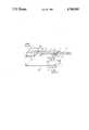
- the FIGUREis a perspective view of a module in accordance with the present invention.
- the principles of the present inventionare particularly useful in the module illustrated in the FIGURE.
- the modulehas a substrate with an upper surface or side 11 and a lower surface or side 12.
- a laser diode 2 and a strip waveguide 3, which extends from the laser diode 2 to an out-coupling and in-coupling location 31 on a straight line,are arranged on the upper surface 11 of the substrate 1 which is of a suitable semi-conductor material, for example, InP.
- the out-coupling and in-coupling location 31is established by an end face of the waveguide 3 at a distal end from the laser diode 2.
- the laser diode emissions having, for example, a first wavelength ⁇ 1are guided in the waveguide 3 and can be coupled out, for example, into a glass fiber 5.
- radiation guided in the waveguide or fiber 5 and having a second wavelength ⁇ 2 differing from the laser diode emissionscan be coupled into the waveguide 3 at this location 31.
- an optical diffraction grating 4is arranged on an upper surface 32 of the waveguide 3 and the furrows or ridges 41 of this diffraction grating, which define the grid lines, are oriented perpendicular to the propagation directions R 1 and R 2 of the radiation guided in the waveguide 3.
- the grating 4, for example,can be manufactured by etching. It can also be arranged on the underside of the waveguide 3.
- the grating 4is dimensioned so that first, the laser diode emissions emitted by the laser diode 2 is disturbed as little as possible and secondly, the radiation having the wavelength ⁇ 2 coupled into the strip waveguide 3 from the glass fiber 5, for example, is diffracted in the direction towards the surface or underside of the substrate 1.
- a photo diode or detector 6is arranged on this underside or surface 12 at a point of incidence of the radiation having the wavelength ⁇ 2 , which radiation is diffracted by the grating 4.
- the grating 4is dimensioned so that the principal direction R 3 of the radiation having the wavelength ⁇ 2 diffracted by it in a direction obliquely down such that it has a horizontal component R 31 , which is parallel to the waveguide 3, that is directed away from the laser diode 2.
- the laser diode 2 and of the strip waveguide 3 with the grating 4for example, layers of the laser diode of, for example, InGaAsP of different compositions can be applied, for example, by means of suitable combination of epitaxy, masking and etching steps. Actual examples of the process of making the laser diode by these steps are disclosed in the above mentioned copending U.S. application, Ser. No. 812,468.
- the strip waveguide 3can also be executed as a strip-loaded film waveguide or as a ribbon waveguide.
- the laser diode 2is preferably provided with a distributed feedback.
- the strip waveguide 3 and the grating 4are covered by a passivating layer 7 of, for example, Si 3 N 4 or InP and are protected by this layer.
- the photo diode 6can be applied by a combination of epitaxy, masking and etching steps. It will have its pn-junction extending parallel to the lower surface 12 of the substrate 1.
Landscapes
- Physics & Mathematics (AREA)
- Engineering & Computer Science (AREA)
- General Physics & Mathematics (AREA)
- Optics & Photonics (AREA)
- Microelectronics & Electronic Packaging (AREA)
- Computer Networks & Wireless Communication (AREA)
- Signal Processing (AREA)
- Optical Couplings Of Light Guides (AREA)
- Optical Integrated Circuits (AREA)
- Optical Communication System (AREA)
- Semiconductor Lasers (AREA)
Abstract
Description
The present invention is directed to an integrated optical multiplex-demultiplex module for bi-directional optical communication transmission. The module includes a laser diode and a strip waveguide for guiding the laser emissions to an out-coupling region being located on one surface of a substrate and a photodetector being arranged on an opposite surface of the substrate. The module has a grating arrangement which is frequency-selective and essentially does not influence the guided laser diode emissions of a first wavelength but it will influence radiation of a second wavelength which is different from the first wavelength which radiation is coupled into the in-coupling location from an external waveguide. The module also has a deflecting diffraction grating having grid lines proceding perpendicular relative to the propagation direction of the radiation in the strip or film waveguide and diffracts and guides the radiation having a second wavelength differing from the laser emissions to the detector on the opposite surface.
A multiplex-demultiplex module or muldex module which has a substrate with a laser diode and a strip waveguide on one surface and a photodetector on an opposite surface with the strip waveguide being provided with a frequency-selective grating for passing the emission of the laser diode and deflecting radiation of a wavelength different from the wavelength of the laser diode which has been coupling into the in-coupling location and having a second deflecting diffraction grating whose grid lines extend perpendicular to the propagation direction in the strip for diffracting the different wavelength onto the photo diode is disclosed in copending U.S. patent application, Ser. No. 812,468, filed Dec. 23, 1985, which U.S. application claims priority from earlier filed European application No. 85111386. In the module disclosed in the above mentioned U.S. application, the grid lines of the frequency-selective diffraction grating proceed obliquely relative to the propagation direction of the radiation guided in the strip waveguide leading from the laser diode to the in-coupling location. A radiation guided in this one waveguide and having a wavelength differing from the wavelength of the laser diode emissions is laterally coupled out of the waveguide by the frequency-selective grating into a second or additional strip waveguide which is arranged on the same side of the substrate and branches off from the one waveguide. The diverting diffraction grating is arranged on this additional waveguide. The grid lines of this second diffraction grating proceed perpendicular to the propagation direction of the radiation conducted in this waveguide. This second diffraction grating steers the radiation onto the photodetector which is the form of a photo diode. In the embodiment of the module, the photo diode is arranged on the side of the substrate lying opposite the one side on which the laser diode and the waveguide with the gratings are arranged. The diverting grating on the second waveguide is dimensioned such that the radiation coupled out by the frequency selective grating and guided in the additional waveguide is steered through the substrate onto the diode.
An integrated optical muldex module, wherein the laser diode, a film waveguide conducting the laser diode emissions to an in-coupling and out-coupling location and a photo diode are arranged on one side of a substrate is disclosed in an article by H. G. Unger, "Planar and Integrated Multi- and Demultiplexers" Proceedings of the 6th European Conference on Circuit Theory and Design, 6-8 September 1983, VDE-Verlag, Berlin, pages 387-389. A frequency-selective diffraction grating is arranged on the film or layer waveguide and this grating in contrast to the module of the type initially discussed guides the laser diode emission in the direction towards the out-coupling locations but does not influence a radiation supply from the in-coupling location and having a wavelength differing from the wavelength of the laser diode emission. The grid lines of the frequency-selective grating proceed obliquely relative to the propagation direction of the radiation and are also curved so that the divergent laser diode emission is convergent after the deflection by the grating. The photo diode appears as though they are arranged in the beam path of the radiation not influenced by the frequency-selective grating have a wavelength differing from the wavelength of the laser diode emisssion. The diffraction grating which steers this radiation to the diode does not seem to be present.
The object of the present invention is to design a muldex module of a species of the initially disclosed manner with a simpler structure.
This is accomplished by an improvement in an integrated optical multiplex-demultiplex module for bi-directional optical communication transmission, said module having a laser diode, a strip first waveguide for guiding a laser diode emission to an out-coupling and in-coupling location being arranged on a surface of a substrate and a photodetector being arranged on the opposite surface of the substrate, a frequency-selective grating being arranged on or in the first waveguide, said frequency-selective grating essentially not influencing the guided laser diode emission but deflects or couples the radiation supplied from the in-coupling location having a wavelength differing from the wavelength of the laser diode emission out of the first waveguide into a second waveguide branching therefrom and a deflecting diffracting grating having grid lines proceeding perpendicular relative to the propagation direction of the radiation of the different waveguides traveling in the additional waveguide being provided on this additional waveguide on the one surface of the substrate and diffracting the radiation through the substrate onto a detector. The improvements are that the frequency-selective grating and the diffracting grating are formed in common by a single grating which is fashioned on or in the first mentioned waveguide leading from the laser diode to the in-coupling location and that the grid lines of this common single grating extend perpendicular to the propagation direction of the radiation in this waveguide.
The module of the invention requires only one strip waveguide and manages with a single grating which assumes the function of both the frequency-selective grating as well as the function of the diffraction grating. The grid lines are straight and proceed perpendicular to the propagation direction of the radiation conducted in the waveguide. This structure simplifies the manufacturing of the grating.
Given a multiplex module under consideration, the radiation-sensitive detectors should be arranged as far as possible from the laser diode. An embodiment of the improvement as the common grating being dimensioned so that a principal direction of radiation supplied from the in-coupling location and diffracted into the substrate by the common grating and having the wavelength differing from the wavelength of the laser diode emission has a component which is directed away from the laser diode.
The FIGURE is a perspective view of a module in accordance with the present invention.
The principles of the present invention are particularly useful in the module illustrated in the FIGURE. The module has a substrate with an upper surface orside 11 and a lower surface orside 12. A laser diode 2 and astrip waveguide 3, which extends from the laser diode 2 to an out-coupling and in-coupling location 31 on a straight line, are arranged on theupper surface 11 of thesubstrate 1 which is of a suitable semi-conductor material, for example, InP. The out-coupling and in-coupling location 31 is established by an end face of thewaveguide 3 at a distal end from the laser diode 2.
At this in-coupling, out-coupling location orregion 31, the laser diode emissions having, for example, a first wavelength λ1 are guided in thewaveguide 3 and can be coupled out, for example, into a glass fiber 5. On the other hand, radiation guided in the waveguide or fiber 5 and having a second wavelength λ2 differing from the laser diode emissions can be coupled into thewaveguide 3 at thislocation 31.
As illustrated, an optical diffraction grating 4 is arranged on anupper surface 32 of thewaveguide 3 and the furrows or ridges 41 of this diffraction grating, which define the grid lines, are oriented perpendicular to the propagation directions R1 and R2 of the radiation guided in thewaveguide 3. The grating 4, for example, can be manufactured by etching. It can also be arranged on the underside of thewaveguide 3.
The grating 4 is dimensioned so that first, the laser diode emissions emitted by the laser diode 2 is disturbed as little as possible and secondly, the radiation having the wavelength λ2 coupled into thestrip waveguide 3 from the glass fiber 5, for example, is diffracted in the direction towards the surface or underside of thesubstrate 1.
A photo diode ordetector 6 is arranged on this underside orsurface 12 at a point of incidence of the radiation having the wavelength λ2, which radiation is diffracted by the grating 4.
In order to produce the greatest possible distance between the laser diode 2 and thephoto diode 6, the grating 4 is dimensioned so that the principal direction R3 of the radiation having the wavelength λ2 diffracted by it in a direction obliquely down such that it has a horizontal component R31, which is parallel to thewaveguide 3, that is directed away from the laser diode 2.
For the manufacture of the laser diode 2 and of thestrip waveguide 3 with the grating 4, for example, layers of the laser diode of, for example, InGaAsP of different compositions can be applied, for example, by means of suitable combination of epitaxy, masking and etching steps. Actual examples of the process of making the laser diode by these steps are disclosed in the above mentioned copending U.S. application, Ser. No. 812,468. Thestrip waveguide 3 can also be executed as a strip-loaded film waveguide or as a ribbon waveguide. The laser diode 2 is preferably provided with a distributed feedback.
Thestrip waveguide 3 and the grating 4 are covered by a passivating layer 7 of, for example, Si3 N4 or InP and are protected by this layer.
Thephoto diode 6 can be applied by a combination of epitaxy, masking and etching steps. It will have its pn-junction extending parallel to thelower surface 12 of thesubstrate 1.
Although various minor modifications may be suggested by those versed in the art, it should be understood that I wish to embody with the scope of the patent granted hereon, all such modifications as reasonably and properly come within the scope of my contribution to the art.
Claims (4)
1. In an integrated optical multiplex-demultiplex module particularly useful for bi-directional optical communication transmissions, said module having a substrate with a laser diode and a strip waveguide for guiding output from the laser diode to an out-coupling region disposed on one surface of the substrate and a photodetector arranged on an opposite surface of the substrate, a frequency-selective grating being arranged in said waveguide and said frequency-selective grating essentially not influencing the guided laser diode emissions traveling in the waveguide to an in-coupling region but deflecting a wavelength different than the wavelength of the laser diode emissions into a second waveguide extending from the first mentioned waveguide and a diffraction grating having grid lines proceeding perpendicular relative to the propagation direction of the radiation of this other wavelength traveling in the second waveguide, said diffraction grating directing the other wavelength onto the photodetector, the improvements comprising said frequency-selective grating and said diffraction grating being formed by a common single grating, which is fashioned on the first waveguide leading from the laser diode to the out-coupling and in-coupling regions, said single grating having grid lines extending perpendicular to the propagation direction of the light in said first waveguide.
2. In an integrated optical multiplex-demultiplex module according to claim 1, wherein said single grating is dimensioned so that the principle direction of the other wavelength, which differs from the wavelength of the laser diode, is suplied from said in-coupling region and is deflected by said single grating into said substrate, has a component extending parallel to the first waveguide directed away from said laser diode.
3. An integrated optical multiplex-demultiplex module for use in bi-directional optical communication transmission, said module having a substrate with a first surface and a second opposite surface, a laser diode emitting emissions of a first wavelength being disposed on said first surface, a waveguide extending from said laser diode to an out-coupling and in-coupling region remote from said laser diode, a photodetector being arranged on the second surface of said substrate, a common grating being disposed on said waveguide, said common grating being a frequency-selective grating essentially not influencing the emissions of the first wavelength from the laser diode traveling in said waveguide to the coupling region and deflecting radiation of a second wavelength differing from said first wavelength, said radiation being coupled at said region into said first waveguide and said common grating also being a diffraction grating for diffracting the radiation of the second wavelength from the waveguide through the substrate to the photo detector, said common grating having grid lines extending perpendicular to the propagation direction of the emissions of the first wavelength and radiation of the second wavelength.
4. An integrated optical multiplex-demultiplex module according to claim 3, wherein said grating is dimensioned so that a principal direction of the diffracted radiation of the second wavelength has a component extending parallel to the first wavelength directed away from said laser diode.
Applications Claiming Priority (2)
| Application Number | Priority Date | Filing Date | Title |
|---|---|---|---|
| DE3543589 | 1985-12-10 | ||
| DE3543589 | 1985-12-10 |
Publications (1)
| Publication Number | Publication Date |
|---|---|
| US4760569Atrue US4760569A (en) | 1988-07-26 |
Family
ID=6288089
Family Applications (1)
| Application Number | Title | Priority Date | Filing Date |
|---|---|---|---|
| US06/937,417Expired - Fee RelatedUS4760569A (en) | 1985-12-10 | 1986-12-03 | Integrated optical multiplex-demultiplex module for optical communications transmission |
Country Status (4)
| Country | Link |
|---|---|
| US (1) | US4760569A (en) |
| EP (1) | EP0226868B1 (en) |
| JP (1) | JPS62139383A (en) |
| DE (1) | DE3687162D1 (en) |
Cited By (56)
| Publication number | Priority date | Publication date | Assignee | Title |
|---|---|---|---|---|
| US4860294A (en)* | 1987-03-30 | 1989-08-22 | Siemens Aktiengesellschaft | Integrated-optical arrangement for bidirectional optical message or signal transmission |
| US4887255A (en)* | 1986-08-25 | 1989-12-12 | Canon Kabushiki Kaisha | Integrated optical head |
| US4904036A (en)* | 1988-03-03 | 1990-02-27 | American Telephone And Telegraph Company, At&T Bell Laboratories | Subassemblies for optoelectronic hybrid integrated circuits |
| US4911512A (en)* | 1986-11-05 | 1990-03-27 | Sharp Kabushiki Kaisha | Waveguide type optical head |
| US4911516A (en)* | 1989-02-27 | 1990-03-27 | General Electric Company | Optical device with mode selecting grating |
| US4916497A (en)* | 1988-05-18 | 1990-04-10 | Harris Corporation | Integrated circuits including photo-optical devices and pressure transducers and method of fabrication |
| US4969712A (en)* | 1989-06-22 | 1990-11-13 | Northern Telecom Limited | Optoelectronic apparatus and method for its fabrication |
| US4989935A (en)* | 1988-09-30 | 1991-02-05 | Siemens Aktiengesellschaft | Optoelectronic transmitter and receiver |
| US5037765A (en)* | 1988-05-18 | 1991-08-06 | Harris Corporation | Method of fabricating integrated circuits including photo optical devices and pressure transducers |
| US5048913A (en)* | 1989-12-26 | 1991-09-17 | United Technologies Corporation | Optical waveguide embedded transverse spatial mode discrimination filter |
| US5070596A (en)* | 1988-05-18 | 1991-12-10 | Harris Corporation | Integrated circuits including photo-optical devices and pressure transducers and method of fabrication |
| US5127081A (en)* | 1990-08-03 | 1992-06-30 | At&T Bell Laboratories | Optical branching waveguide |
| US5131060A (en)* | 1990-07-09 | 1992-07-14 | Canon Kabushiki Kaisha | Optical waveguide modulator communications device and method of modulating light using same |
| US5134671A (en)* | 1990-08-03 | 1992-07-28 | At&T Bell Laboratories | Monolithic integrated optical amplifier and photodetector |
| US5193131A (en)* | 1991-04-30 | 1993-03-09 | France Telecom Etablissement Autonome De Droit Public | Optoelectronic device with an integrated optical guide and photodetector |
| US5206920A (en)* | 1991-02-01 | 1993-04-27 | Siemens Aktiengesellschaft | Integrated optical arrangement for demultiplexing a plurality of different wavelength channels and the method of manufacture |
| US5245404A (en)* | 1990-10-18 | 1993-09-14 | Physical Optics Corportion | Raman sensor |
| US5303316A (en)* | 1989-12-22 | 1994-04-12 | David Sarnoff Research Center, Inc. | Optical beam scanner |
| US5355237A (en)* | 1993-03-17 | 1994-10-11 | The United States Of America As Represented By The Administrator Of The National Aeronautics And Space Administration | Wavelength-division multiplexed optical integrated circuit with vertical diffraction grating |
| US5500910A (en)* | 1994-06-30 | 1996-03-19 | The Whitaker Corporation | Passively aligned holographic WDM |
| US5555127A (en)* | 1994-06-30 | 1996-09-10 | The Whitaker Corporation | Planar hybrid optical amplifier |
| US5771254A (en)* | 1996-01-25 | 1998-06-23 | Hewlett-Packard Company | Integrated controlled intensity laser-based light source |
| US5809050A (en)* | 1996-01-25 | 1998-09-15 | Hewlett-Packard Company | Integrated controlled intensity laser-based light source using diffraction, scattering and transmission |
| US6011884A (en)* | 1997-12-13 | 2000-01-04 | Lightchip, Inc. | Integrated bi-directional axial gradient refractive index/diffraction grating wavelength division multiplexer |
| US6011885A (en)* | 1997-12-13 | 2000-01-04 | Lightchip, Inc. | Integrated bi-directional gradient refractive index wavelength division multiplexer |
| US6137933A (en)* | 1997-12-13 | 2000-10-24 | Lightchip, Inc. | Integrated bi-directional dual axial gradient refractive index/diffraction grating wavelength division multiplexer |
| US6236780B1 (en) | 1997-12-13 | 2001-05-22 | Light Chip, Inc. | Wavelength division multiplexing/demultiplexing devices using dual diffractive optic lenses |
| US6243513B1 (en) | 1997-12-13 | 2001-06-05 | Lightchip, Inc. | Wavelength division multiplexing/demultiplexing devices using diffractive optic lenses |
| US6263135B1 (en) | 1997-12-13 | 2001-07-17 | Lightchip, Inc. | Wavelength division multiplexing/demultiplexing devices using high index of refraction crystalline lenses |
| US6271970B1 (en) | 1997-12-13 | 2001-08-07 | Lightchip, Inc. | Wavelength division multiplexing/demultiplexing devices using dual homogeneous refractive index lenses |
| US6289155B1 (en) | 1997-12-13 | 2001-09-11 | Lightchip, Inc. | Wavelength division multiplexing/demultiplexing devices using dual high index of refraction crystalline lenses |
| US6298182B1 (en) | 1997-12-13 | 2001-10-02 | Light Chip, Inc. | Wavelength division multiplexing/demultiplexing devices using polymer lenses |
| US6324329B1 (en)* | 1998-08-28 | 2001-11-27 | Sony Corporation | Photocatalyst excitation apparatus |
| US6343169B1 (en) | 1999-02-25 | 2002-01-29 | Lightchip, Inc. | Ultra-dense wavelength division multiplexing/demultiplexing device |
| US6404945B1 (en) | 1997-12-13 | 2002-06-11 | Lightchip, Inc. | Wavelength division multiplexing/demultiplexing devices using homogeneous refractive index lenses |
| US6415073B1 (en) | 2000-04-10 | 2002-07-02 | Lightchip, Inc. | Wavelength division multiplexing/demultiplexing devices employing patterned optical components |
| US6434299B1 (en) | 1999-06-01 | 2002-08-13 | Lightchip, Inc. | Wavelength division multiplexing/demultiplexing devices having concave diffraction gratings |
| US6480648B1 (en) | 1999-02-25 | 2002-11-12 | Lightchip, Inc. | Technique for detecting the status of WDM optical signals |
| WO2002095469A1 (en)* | 2001-05-23 | 2002-11-28 | Infineon Technologies Ag | Module for an optical signal transmission |
| US6490393B1 (en)* | 2000-11-27 | 2002-12-03 | Advanced Interfaces, Llc | Integrated optical multiplexer and demultiplexer for wavelength division transmission of information |
| US20030053736A1 (en)* | 2001-09-20 | 2003-03-20 | Yoshiki Kuhara | Optical waveguide-integrated substrate, method for producing the substrate, and optical transceiver using the substrate |
| EP1009119A3 (en)* | 1998-12-10 | 2003-08-27 | Nortel Networks Limited | Integration of Optical Add Drop Multiplexing filters |
| US20040008748A1 (en)* | 2002-07-11 | 2004-01-15 | Andrew Harker | Wavelength detector apparatus and method therefor |
| US20040184732A1 (en)* | 2000-11-27 | 2004-09-23 | Advanced Interfaces, Llc | Integrated optical multiplexer and demultiplexer for wavelength division transmission of information |
| US6829096B1 (en) | 1999-02-25 | 2004-12-07 | Confluent Photonics Corporation | Bi-directional wavelength division multiplexing/demultiplexing devices |
| FR2873454A1 (en)* | 2004-07-26 | 2006-01-27 | E Klo Sarl | Photoreceptor component, has waveguides interposed between photodiodes and optical fiber, where waveguides and photodiodes are formed on same substrate and each waveguide has end partially covering active surface of respective photodiode |
| US20070286549A1 (en)* | 2004-02-17 | 2007-12-13 | Yoshihisa Warashina | Optical Transmitting /Receiving Module |
| US20100021108A1 (en)* | 2008-07-22 | 2010-01-28 | Kang Hyun-Seo | Optical waveguide device and optical communication module |
| US20100135614A1 (en)* | 2008-11-28 | 2010-06-03 | Lee Sei-Hyoung | Optical waveguide and bi-directional optical transceiver |
| EP2216663A1 (en)* | 2009-02-09 | 2010-08-11 | Commissariat à l'Énergie Atomique et aux Énergies Alternatives | Structure and method of aligning an optical fibre with a sub-micronic optical waveguide |
| US20110052114A1 (en)* | 2009-09-02 | 2011-03-03 | Alcatel-Lucent Usa Inc. | Vertical optically emitting photonic devices with electronic steering capability |
| US20110135313A1 (en)* | 2009-12-04 | 2011-06-09 | I Shou University | Optical fiber communication method and transmitting device |
| FR2965939A1 (en)* | 2010-10-12 | 2012-04-13 | Commissariat Energie Atomique | NANOPHOTONIC OPTICAL DUPLEXER |
| US20140221846A1 (en)* | 1999-03-23 | 2014-08-07 | Shabbir Bambot | System and method for determining tissue characteristics |
| GB2561590A (en)* | 2017-04-19 | 2018-10-24 | Quantum Base Ltd | A photonic device |
| FR3155915A1 (en)* | 2023-11-28 | 2025-05-30 | Latelec | Fiber optic device |
Families Citing this family (4)
| Publication number | Priority date | Publication date | Assignee | Title |
|---|---|---|---|---|
| DE3701863A1 (en)* | 1987-01-23 | 1988-08-04 | Standard Elektrik Lorenz Ag | Transmitter for coherent optical communications |
| DE3730971A1 (en)* | 1987-09-15 | 1989-03-23 | Siemens Ag | WAVELENGTH MULDEX ARRANGEMENT |
| JPH0669491A (en)* | 1992-08-18 | 1994-03-11 | Fujitsu Ltd | Optical transceiver |
| DE4440088A1 (en)* | 1994-11-10 | 1996-05-15 | Telefunken Microelectron | Semiconductor module for bidirectional, line-bound, optical data transmission |
Citations (2)
| Publication number | Priority date | Publication date | Assignee | Title |
|---|---|---|---|---|
| JPS5937520A (en)* | 1982-08-26 | 1984-03-01 | Nec Corp | Wavelength multiplex demultiplexer |
| US4640574A (en)* | 1982-08-25 | 1987-02-03 | Ant Nachrichtentechnik Gmbh | Integrated, micro-optical device |
Family Cites Families (1)
| Publication number | Priority date | Publication date | Assignee | Title |
|---|---|---|---|---|
| FR2426922A1 (en)* | 1978-05-26 | 1979-12-21 | Thomson Csf | COMPACT OPTICAL STRUCTURE WITH INTEGRATED SOURCE |
- 1986
- 1986-11-27DEDE8686116522Tpatent/DE3687162D1/ennot_activeExpired - Fee Related
- 1986-11-27EPEP86116522Apatent/EP0226868B1/ennot_activeExpired - Lifetime
- 1986-12-03USUS06/937,417patent/US4760569A/ennot_activeExpired - Fee Related
- 1986-12-05JPJP61291403Apatent/JPS62139383A/enactivePending
Patent Citations (2)
| Publication number | Priority date | Publication date | Assignee | Title |
|---|---|---|---|---|
| US4640574A (en)* | 1982-08-25 | 1987-02-03 | Ant Nachrichtentechnik Gmbh | Integrated, micro-optical device |
| JPS5937520A (en)* | 1982-08-26 | 1984-03-01 | Nec Corp | Wavelength multiplex demultiplexer |
Non-Patent Citations (8)
| Title |
|---|
| Fl gge, Encyclopedia of Physics , vol. XXIX, Optical Instruments, Springer Verlag, Berlin Heidelberg New York, 1967, pp. 564 610.* |
| Flanders et al., "Grating Filters for Thin-Film Optical Waveguides", Applied Physics Letters, vol. 24, No. 4, 15 Feb. 1974, pp. 194-196. |
| Flanders et al., Grating Filters for Thin Film Optical Waveguides , Applied Physics Letters , vol. 24, No. 4, 15 Feb. 1974, pp. 194 196.* |
| Flugge, Encyclopedia of Physics, vol. XXIX, Optical Instruments, Springer-Verlag, Berlin-Heidelberg-New York, 1967, pp. 564-610. |
| Tamir, "3. Beam and Waveguide Couplers", Integrated Optics, Springer-Verlag Berlin, Heidelberg, New York, 1975, pp. 83-135. |
| Tamir, 3. Beam and Waveguide Couplers , Integrated Optics , Springer Verlag Berlin, Heidelberg, New York, 1975, pp. 83 135.* |
| Unger, "Planar and Integrated Multi-and Demultiplexers", Proceedings of the Sixth European Conference on Circuit Theory and Design, Sep. 6-8, 1983, VDE-Verlag GmbH, Berlin, pp. 387-389. |
| Unger, Planar and Integrated Multi and Demultiplexers , Proceedings of the Sixth European Conference on Circuit Theory and Design , Sep. 6 8, 1983, VDE Verlag GmbH, Berlin, pp. 387 389.* |
Cited By (77)
| Publication number | Priority date | Publication date | Assignee | Title |
|---|---|---|---|---|
| US4887255A (en)* | 1986-08-25 | 1989-12-12 | Canon Kabushiki Kaisha | Integrated optical head |
| US4911512A (en)* | 1986-11-05 | 1990-03-27 | Sharp Kabushiki Kaisha | Waveguide type optical head |
| US4860294A (en)* | 1987-03-30 | 1989-08-22 | Siemens Aktiengesellschaft | Integrated-optical arrangement for bidirectional optical message or signal transmission |
| US4904036A (en)* | 1988-03-03 | 1990-02-27 | American Telephone And Telegraph Company, At&T Bell Laboratories | Subassemblies for optoelectronic hybrid integrated circuits |
| US5070596A (en)* | 1988-05-18 | 1991-12-10 | Harris Corporation | Integrated circuits including photo-optical devices and pressure transducers and method of fabrication |
| US5037765A (en)* | 1988-05-18 | 1991-08-06 | Harris Corporation | Method of fabricating integrated circuits including photo optical devices and pressure transducers |
| US4916497A (en)* | 1988-05-18 | 1990-04-10 | Harris Corporation | Integrated circuits including photo-optical devices and pressure transducers and method of fabrication |
| US4989935A (en)* | 1988-09-30 | 1991-02-05 | Siemens Aktiengesellschaft | Optoelectronic transmitter and receiver |
| US4911516A (en)* | 1989-02-27 | 1990-03-27 | General Electric Company | Optical device with mode selecting grating |
| US4969712A (en)* | 1989-06-22 | 1990-11-13 | Northern Telecom Limited | Optoelectronic apparatus and method for its fabrication |
| EP0404301B1 (en)* | 1989-06-22 | 1994-08-10 | Nortel Networks Corporation | Optoelectronic apparatus and method for its fabrication |
| US5303316A (en)* | 1989-12-22 | 1994-04-12 | David Sarnoff Research Center, Inc. | Optical beam scanner |
| US5048913A (en)* | 1989-12-26 | 1991-09-17 | United Technologies Corporation | Optical waveguide embedded transverse spatial mode discrimination filter |
| US5131060A (en)* | 1990-07-09 | 1992-07-14 | Canon Kabushiki Kaisha | Optical waveguide modulator communications device and method of modulating light using same |
| US5127081A (en)* | 1990-08-03 | 1992-06-30 | At&T Bell Laboratories | Optical branching waveguide |
| US5134671A (en)* | 1990-08-03 | 1992-07-28 | At&T Bell Laboratories | Monolithic integrated optical amplifier and photodetector |
| US5245404A (en)* | 1990-10-18 | 1993-09-14 | Physical Optics Corportion | Raman sensor |
| US5206920A (en)* | 1991-02-01 | 1993-04-27 | Siemens Aktiengesellschaft | Integrated optical arrangement for demultiplexing a plurality of different wavelength channels and the method of manufacture |
| US5193131A (en)* | 1991-04-30 | 1993-03-09 | France Telecom Etablissement Autonome De Droit Public | Optoelectronic device with an integrated optical guide and photodetector |
| US5355237A (en)* | 1993-03-17 | 1994-10-11 | The United States Of America As Represented By The Administrator Of The National Aeronautics And Space Administration | Wavelength-division multiplexed optical integrated circuit with vertical diffraction grating |
| US5500910A (en)* | 1994-06-30 | 1996-03-19 | The Whitaker Corporation | Passively aligned holographic WDM |
| US5555127A (en)* | 1994-06-30 | 1996-09-10 | The Whitaker Corporation | Planar hybrid optical amplifier |
| US5771254A (en)* | 1996-01-25 | 1998-06-23 | Hewlett-Packard Company | Integrated controlled intensity laser-based light source |
| US5809050A (en)* | 1996-01-25 | 1998-09-15 | Hewlett-Packard Company | Integrated controlled intensity laser-based light source using diffraction, scattering and transmission |
| US6289155B1 (en) | 1997-12-13 | 2001-09-11 | Lightchip, Inc. | Wavelength division multiplexing/demultiplexing devices using dual high index of refraction crystalline lenses |
| US6580856B1 (en) | 1997-12-13 | 2003-06-17 | Confluent Photonics Corporation | Wavelength division multiplexing/demultiplexing devices using homogeneous refractive index lenses |
| US6137933A (en)* | 1997-12-13 | 2000-10-24 | Lightchip, Inc. | Integrated bi-directional dual axial gradient refractive index/diffraction grating wavelength division multiplexer |
| US6236780B1 (en) | 1997-12-13 | 2001-05-22 | Light Chip, Inc. | Wavelength division multiplexing/demultiplexing devices using dual diffractive optic lenses |
| US6243513B1 (en) | 1997-12-13 | 2001-06-05 | Lightchip, Inc. | Wavelength division multiplexing/demultiplexing devices using diffractive optic lenses |
| US6263135B1 (en) | 1997-12-13 | 2001-07-17 | Lightchip, Inc. | Wavelength division multiplexing/demultiplexing devices using high index of refraction crystalline lenses |
| US6271970B1 (en) | 1997-12-13 | 2001-08-07 | Lightchip, Inc. | Wavelength division multiplexing/demultiplexing devices using dual homogeneous refractive index lenses |
| US6011884A (en)* | 1997-12-13 | 2000-01-04 | Lightchip, Inc. | Integrated bi-directional axial gradient refractive index/diffraction grating wavelength division multiplexer |
| US6298182B1 (en) | 1997-12-13 | 2001-10-02 | Light Chip, Inc. | Wavelength division multiplexing/demultiplexing devices using polymer lenses |
| US6011885A (en)* | 1997-12-13 | 2000-01-04 | Lightchip, Inc. | Integrated bi-directional gradient refractive index wavelength division multiplexer |
| US6404945B1 (en) | 1997-12-13 | 2002-06-11 | Lightchip, Inc. | Wavelength division multiplexing/demultiplexing devices using homogeneous refractive index lenses |
| US6324329B1 (en)* | 1998-08-28 | 2001-11-27 | Sony Corporation | Photocatalyst excitation apparatus |
| EP1009119A3 (en)* | 1998-12-10 | 2003-08-27 | Nortel Networks Limited | Integration of Optical Add Drop Multiplexing filters |
| US6343169B1 (en) | 1999-02-25 | 2002-01-29 | Lightchip, Inc. | Ultra-dense wavelength division multiplexing/demultiplexing device |
| US6480648B1 (en) | 1999-02-25 | 2002-11-12 | Lightchip, Inc. | Technique for detecting the status of WDM optical signals |
| US6829096B1 (en) | 1999-02-25 | 2004-12-07 | Confluent Photonics Corporation | Bi-directional wavelength division multiplexing/demultiplexing devices |
| US6591040B1 (en) | 1999-02-25 | 2003-07-08 | Confluent Photonics Corporation | Ultra-dense wavelength division multiplexing/demultiplexing devices |
| US20140221846A1 (en)* | 1999-03-23 | 2014-08-07 | Shabbir Bambot | System and method for determining tissue characteristics |
| US6434299B1 (en) | 1999-06-01 | 2002-08-13 | Lightchip, Inc. | Wavelength division multiplexing/demultiplexing devices having concave diffraction gratings |
| US6594415B1 (en)* | 2000-04-10 | 2003-07-15 | Confluent Photonics Corporation | Wavelength division multiplexing/demultiplexing devices employing patterned optical components |
| US6415073B1 (en) | 2000-04-10 | 2002-07-02 | Lightchip, Inc. | Wavelength division multiplexing/demultiplexing devices employing patterned optical components |
| US20040184732A1 (en)* | 2000-11-27 | 2004-09-23 | Advanced Interfaces, Llc | Integrated optical multiplexer and demultiplexer for wavelength division transmission of information |
| US20030086649A1 (en)* | 2000-11-27 | 2003-05-08 | Advanced Interfaces, Inc. | Integrated optical multiplexer and demultiplexer for wavelength division transmission of information |
| US6490393B1 (en)* | 2000-11-27 | 2002-12-03 | Advanced Interfaces, Llc | Integrated optical multiplexer and demultiplexer for wavelength division transmission of information |
| US7050675B2 (en) | 2000-11-27 | 2006-05-23 | Advanced Interfaces, Llc | Integrated optical multiplexer and demultiplexer for wavelength division transmission of information |
| US6718093B2 (en) | 2000-11-27 | 2004-04-06 | Advanced Interfaces, Llc | Integrated optical multiplexer and demultiplexer for wavelength division transmission of information |
| US6614963B2 (en) | 2001-05-23 | 2003-09-02 | Infineon Technologies Ag | Module for optical signal transmission |
| WO2002095469A1 (en)* | 2001-05-23 | 2002-11-28 | Infineon Technologies Ag | Module for an optical signal transmission |
| DE10196455B4 (en)* | 2001-05-23 | 2006-11-16 | Infineon Technologies Ag | Module for optical signal transmission |
| US6859601B2 (en)* | 2001-09-20 | 2005-02-22 | Sumitomo Electric Industries, Ltd. | Optical waveguide-integrated substrate, method for producing the substrate, and optical transceiver using the substrate |
| US20030053736A1 (en)* | 2001-09-20 | 2003-03-20 | Yoshiki Kuhara | Optical waveguide-integrated substrate, method for producing the substrate, and optical transceiver using the substrate |
| US20040008748A1 (en)* | 2002-07-11 | 2004-01-15 | Andrew Harker | Wavelength detector apparatus and method therefor |
| US20070286549A1 (en)* | 2004-02-17 | 2007-12-13 | Yoshihisa Warashina | Optical Transmitting /Receiving Module |
| US7486846B2 (en)* | 2004-02-17 | 2009-02-03 | Hammatsu Photonics K.K. | Optical transmitting /receiving module |
| FR2873454A1 (en)* | 2004-07-26 | 2006-01-27 | E Klo Sarl | Photoreceptor component, has waveguides interposed between photodiodes and optical fiber, where waveguides and photodiodes are formed on same substrate and each waveguide has end partially covering active surface of respective photodiode |
| EP1621906A1 (en)* | 2004-07-26 | 2006-02-01 | E-Klo | Device including a flush-mounted optoelectronic element covered by a waveguide |
| US20100021108A1 (en)* | 2008-07-22 | 2010-01-28 | Kang Hyun-Seo | Optical waveguide device and optical communication module |
| US7792401B2 (en) | 2008-07-22 | 2010-09-07 | Electronics And Telecommunications Research Institute | Optical waveguide device and optical communication module |
| US7995883B2 (en) | 2008-11-28 | 2011-08-09 | Electronics And Telecommunications Research Institute | Optical waveguide and bi-directional optical transceiver |
| US20100135614A1 (en)* | 2008-11-28 | 2010-06-03 | Lee Sei-Hyoung | Optical waveguide and bi-directional optical transceiver |
| US20100202738A1 (en)* | 2009-02-09 | 2010-08-12 | Commissariat A L'energie Atomique | Structure and Method for Aligning an Optical Fiber and a Submicronic Waveguide |
| FR2942047A1 (en)* | 2009-02-09 | 2010-08-13 | Commissariat Energie Atomique | STRUCTURE AND METHOD FOR ALIGNING OPTICAL FIBER AND SUBMICRONIC WAVEGUIDE |
| EP2216663A1 (en)* | 2009-02-09 | 2010-08-11 | Commissariat à l'Énergie Atomique et aux Énergies Alternatives | Structure and method of aligning an optical fibre with a sub-micronic optical waveguide |
| US20110052114A1 (en)* | 2009-09-02 | 2011-03-03 | Alcatel-Lucent Usa Inc. | Vertical optically emitting photonic devices with electronic steering capability |
| US8515217B2 (en)* | 2009-09-02 | 2013-08-20 | Alcatel Lucent | Vertical optically emitting photonic devices with electronic steering capability |
| US8428467B2 (en)* | 2009-12-04 | 2013-04-23 | I Shou University | Optical fiber communication method and transmitting device |
| US20110135313A1 (en)* | 2009-12-04 | 2011-06-09 | I Shou University | Optical fiber communication method and transmitting device |
| FR2965939A1 (en)* | 2010-10-12 | 2012-04-13 | Commissariat Energie Atomique | NANOPHOTONIC OPTICAL DUPLEXER |
| EP2442164A1 (en)* | 2010-10-12 | 2012-04-18 | Commissariat à l'Énergie Atomique et aux Énergies Alternatives | Nanophotonic optical duplexer |
| US8693816B2 (en) | 2010-10-12 | 2014-04-08 | Commissariat A L'energie Atomique Et Aux Energies Alternatives | Nanophotonic optical duplexer |
| GB2561590A (en)* | 2017-04-19 | 2018-10-24 | Quantum Base Ltd | A photonic device |
| FR3155915A1 (en)* | 2023-11-28 | 2025-05-30 | Latelec | Fiber optic device |
| WO2025114341A1 (en)* | 2023-11-28 | 2025-06-05 | Latelec | Fibre-optic optical device |
Also Published As
| Publication number | Publication date |
|---|---|
| EP0226868A3 (en) | 1989-05-24 |
| DE3687162D1 (en) | 1993-01-07 |
| EP0226868B1 (en) | 1992-11-25 |
| JPS62139383A (en) | 1987-06-23 |
| EP0226868A2 (en) | 1987-07-01 |
Similar Documents
| Publication | Publication Date | Title |
|---|---|---|
| US4760569A (en) | Integrated optical multiplex-demultiplex module for optical communications transmission | |
| US4860294A (en) | Integrated-optical arrangement for bidirectional optical message or signal transmission | |
| US4772787A (en) | Monolithically integrated opto-electronic semiconductor component | |
| US4730330A (en) | Integrated structure for bi-directional optical fiber transmission | |
| EP0498169B1 (en) | Opto-electronic device for coupling and uncoupling of radiation | |
| US6316281B1 (en) | Method for fabricating a hybrid optical integrated circuit employing SOI optical waveguide | |
| US4747649A (en) | Monolithically integrated WDM demultiplex module and method of manufacture of such module | |
| EP0469789B1 (en) | Optical branching waveguide | |
| US5838854A (en) | Integrated optical control element and a method for fabricating the same and optical integrated circuit element and optical integrated circuit device using the same | |
| US5640474A (en) | Easily manufacturable optical self-imaging waveguide | |
| WO1997049150A1 (en) | An integrated optical device | |
| US5894538A (en) | Method of forming integrated optical circuit planar waveguide turning mirrors | |
| EP0762157A2 (en) | Optical integrated circuit and method for fabricating the same | |
| US5029297A (en) | Optical amplifier-photodetector device | |
| US6108481A (en) | Optical semiconductor device and its manufacturing method | |
| DE69425857T2 (en) | Optical waveguide mirrors | |
| US6574390B2 (en) | Configuration to multiplex and/or demultiplex the signals of a plurality of optical data channels and method for the production of the configuration | |
| US5157748A (en) | Controllable integrated optical directional coupler | |
| US5151959A (en) | Controllable integrated optical mach-zehnder interferometer | |
| JPH1031127A (en) | Optical device having alignment mark and its production | |
| JPH0430581A (en) | Semiconductor light receiving device | |
| US6091756A (en) | Analog laser assembly | |
| KR100420587B1 (en) | Electro-absorption modulator laser | |
| KR100194584B1 (en) | Semiconductor Lattice Waveguide Structure and Manufacturing Method Thereof | |
| JPH08181350A (en) | Semiconductor optical integrated device |
Legal Events
| Date | Code | Title | Description |
|---|---|---|---|
| AS | Assignment | Owner name:SIEMENS AKTIENGESELLSCHAFT, BERLIN AND MUNICH, A G Free format text:ASSIGNMENT OF ASSIGNORS INTEREST.;ASSIGNOR:MAHLEIN, HANS F.;REEL/FRAME:004647/0953 Effective date:19861014 Owner name:SIEMENS AKTIENGESELLSCHAFT, A GERMAN CORP.,GERMANY Free format text:ASSIGNMENT OF ASSIGNORS INTEREST;ASSIGNOR:MAHLEIN, HANS F.;REEL/FRAME:004647/0953 Effective date:19861014 | |
| FEPP | Fee payment procedure | Free format text:PAYOR NUMBER ASSIGNED (ORIGINAL EVENT CODE: ASPN); ENTITY STATUS OF PATENT OWNER: LARGE ENTITY | |
| FPAY | Fee payment | Year of fee payment:4 | |
| REMI | Maintenance fee reminder mailed | ||
| LAPS | Lapse for failure to pay maintenance fees | ||
| FP | Lapsed due to failure to pay maintenance fee | Effective date:19960731 | |
| STCH | Information on status: patent discontinuation | Free format text:PATENT EXPIRED DUE TO NONPAYMENT OF MAINTENANCE FEES UNDER 37 CFR 1.362 |