US4757519A - Digital premodulation filter - Google Patents
Digital premodulation filterDownload PDFInfo
- Publication number
- US4757519A US4757519AUS07/104,201US10420187AUS4757519AUS 4757519 AUS4757519 AUS 4757519AUS 10420187 AUS10420187 AUS 10420187AUS 4757519 AUS4757519 AUS 4757519A
- Authority
- US
- United States
- Prior art keywords
- signal
- digital
- filter
- coupled
- clock signal
- Prior art date
- Legal status (The legal status is an assumption and is not a legal conclusion. Google has not performed a legal analysis and makes no representation as to the accuracy of the status listed.)
- Expired - Lifetime
Links
- 230000002902bimodal effectEffects0.000claimsabstractdescription26
- 238000005316response functionMethods0.000claimsabstractdescription22
- 230000004044responseEffects0.000claimsabstractdescription17
- 238000003491arrayMethods0.000claimsdescription27
- 230000006870functionEffects0.000claimsdescription24
- 238000005070samplingMethods0.000claimsdescription4
- 210000000352storage cellAnatomy0.000claims10
- 238000001914filtrationMethods0.000claims3
- 210000004027cellAnatomy0.000claims2
- 230000008672reprogrammingEffects0.000claims1
- 238000000034methodMethods0.000description22
- 230000008569processEffects0.000description13
- 238000010586diagramMethods0.000description10
- 238000007792additionMethods0.000description6
- 238000006243chemical reactionMethods0.000description5
- 238000009825accumulationMethods0.000description4
- 238000004891communicationMethods0.000description3
- 230000008520organizationEffects0.000description3
- 238000001228spectrumMethods0.000description2
- 230000003321amplificationEffects0.000description1
- 230000008901benefitEffects0.000description1
- 230000005540biological transmissionEffects0.000description1
- 230000003750conditioning effectEffects0.000description1
- 238000012937correctionMethods0.000description1
- 238000013461designMethods0.000description1
- 238000012986modificationMethods0.000description1
- 230000004048modificationEffects0.000description1
- 238000003199nucleic acid amplification methodMethods0.000description1
- 238000013139quantizationMethods0.000description1
- 238000012546transferMethods0.000description1
- 238000005303weighingMethods0.000description1
Images


Classifications
- H—ELECTRICITY
- H03—ELECTRONIC CIRCUITRY
- H03H—IMPEDANCE NETWORKS, e.g. RESONANT CIRCUITS; RESONATORS
- H03H17/00—Networks using digital techniques
- H03H17/02—Frequency selective networks
- H03H17/0294—Variable filters; Programmable filters
- H—ELECTRICITY
- H03—ELECTRONIC CIRCUITRY
- H03H—IMPEDANCE NETWORKS, e.g. RESONANT CIRCUITS; RESONATORS
- H03H17/00—Networks using digital techniques
- H03H17/02—Frequency selective networks
- H03H17/06—Non-recursive filters
- H03H17/0607—Non-recursive filters comprising a ROM addressed by the input data signals
Definitions
- the present inventionrelates generally to transmitters for transmitting angle modulated signals, and, more particularly, to a digital premodulation filter for conditioning a serial bit stream prior to frequency (or phase) modulation of a RF carrier signal.
- U.S. Pat. No. 4,477,916 entitled “Transmitter for Angle--Modulated Signals” issued to Kah-Seng Chung on Oct. 16, 1984discloses an FM transmitter having a premodulation filter to shape an input data signal in a predetermined manner.
- the premodulation filtercomprises a Gaussian low-pass filter and a correction filter.
- the latter filtercomprises a cascade of 2n delay sections, each having a time delay of T seconds.
- the output of the premodulation filteris connected to the signal input of a frequency modulation circuit to provided the modulated output as desired.
- the premodulation filtercomprises the series arrangement of a non-recursive second order digital filter with three weighing factors, two of which are equal to each other, and a low pass filter realized by means of a "raised cosine" filter which satisfies the first Nyquist criterion.
- the mutually unequal weighting factorshave the values A and B, the value of the weighting factor A and, respectively of the non-recursive second order filter being less than one-fourth and larger than one-half, respectively, 2A+B being equal to one and the roll off coefficient of the "raised cosine" filter being unequal to zero.
- premodulation filter circuitscomprising analog filters or a combination of digital and analog filters to provide carrier modulation dedicated to a single modulation type; TFM, for example.
- CPMcontinuous phase modulation
- Examples of such CPMare minimum shift keying (MSK), Gaussian minimum shift keying (GMSK), tamed frequency modulation (TFM) and four-level FM (4-FM) and additional modulation methods which a user may define.
- the premodulation filter of the present inventionis electronically configurable by a user to perform a desired modulation type, thus providing a more versatile instrument than previous methods which are typically dedicated to a single modulation type.
- the premodulation filterutilizes a finite impulse response filter (FIR) technique to digitally filter an input serial bit data stream.
- FIRfinite impulse response filter
- Each modulation formatsuch as TFM, has a unique impulse response function g(t) which is the response to a single input data bit represented by a single impulse function.
- the premodulation filterpreforms a linear combination of g(t) responses resulting from the input data stream represented by a series of bimodal impulse functions.
- the output of FIR digital filter in the form of parallel digital wordsis coupled to a digital to analog converter (DAC).
- DACdigital to analog converter
- the output of the DACis then passed through an analog filter to provide a smooth analog voltage input to a modulator to vary, for example, the frequency or phase of an oscillator, such as a voltage controlled oscillator (VCO) to provide a digitally modulated carrier output.
- a modulatorsuch as a voltage controlled oscillator (VCO) to provide a digitally modulated carrier output.
- VCOvoltage controlled oscillator
- the prior art premodulation filters described hereinaboveare typically dedicated to a single digital modulation format and are not easily user configurable.
- a number of frequency or phase pulse-shape function g(t) arraysare stored in ROM (or RAM) allowing the user to easily choose any desired modulation format.
- a usermay adjust operational parameters to optimize further performance or to design a custom modulation format for use with a users particular digital communication system.
- prior art digital premodulation FIR filterstypically utilize multiplication in the convolution process whereas the present invention utilizes an adder thus providing a speed advantage over the prior art.
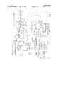
- FIGS. 1a and 1bare block diagrams illustrating an RF transmitter utilizing FM modulation and of an RF transmitter utilizing phase modulation.
- FIG. 2is a block diagram illustrating an RF transmitter utilizing I-Q modulation.
- FIG. 3is a block diagram illustrating a conceptual representation of a FIR digital premodulation filter according to the principals of the present invention.
- FIG. 4is a graphical presentation of an example of a two-level digital modulation impulse response function g(t) and algorithm utilized in the apparatus shown in FIG. 6.
- FIG. 5is graphical representation of an example of a four-level digital modulation impulse response function g(t) and algorithm utilized in the apparatus shown in FIG. 7.
- FIG. 6is a block diagram illustrating the implementation of the FIR premodulation filter algorithm shown in FIG. 4 for two-level digital modulation.
- FIG. 7is block diagram illustrating the implementation of the FIR premodulation filter algorithm shown in FIG. 5 for two-level or four-level digital modulation.
- the method and apparatus described hereinutilizes a Finite Impulse Response (FIR) technique to digitally filter an input data signal.
- the FIR digital premodulation filteris programmable by the user to generate various modulation signals corresponding to several different types of frequency modulation (FM) and phase modulation (PM). Each modulation type or format has a unique impulse response function g(t) which is the response to a single input data impulse.
- the FIR digital premodulation filterperforms a convolution utilizing a linear combination of g(t) responses resulting from the input data stream.
- the input to the FIR digital premodulation filteris in the form of a bimodal impulse stream which represents the input data.
- FIGS. 1A and 1Ba block diagram illustrating a portion 10 of a signal generator which provides a frequency modulated RF carrier signal is shown. It comprises a digital premodulation filter 11 having an input line 17 for receiving a data signal, and an RF carrier generator 15 coupled to a frequency modulator 13. By means of the digital premodulation filter 11, which will be described in greater detail, an analog modulation signal is generated. This modulation signal is coupled to the modulator 13 to frequency modulate the RF carrier signal supplied by the RF carrier generator 15. The FM RF output signal thus formed by modulator 13 is output on line 19.
- FIG. 1Arepresents a frequency modulation system wherein the FIR function g(t) utilized by the digital premodulation filter 11 represents the instantaneous frequency deviation of the RF carrier output signal on line 19 resulting from a single impulse function and can be termed a "frequency pulse shape function”.
- FIG. 1Brepresents a phase modulation system wherein the FIR function g(t) utilized by the digital premodulation filter 11 represents the instantaneous phase deviation of the RF carrier output signal on line 19 resulting from a single impulse function and can be termed "phase pulse shape function”.
- FIR digital premodulation filter 23may be programmed to generate a desired type of modulation wherein g(t) will represent either the instantaneous frequency or phase deviation of the RF output signal resulting from a single impulse function, depending on whether FM or PM operation is used.
- a input data stream on line 21is coupled to the FIR digital premodulation filter 23 which performs a convolution utilizing a linear combination of g(t) responses and outputs a signal in the form of parallel digital words.
- the output of the FIR digital premodulation filter 23is coupled via switch 25 to a modulo 2 PI transform network and accumulator 27 to transform the instantaneous frequency deviation to an instantaneous phase deviation.
- the accumulator 27 outputis coupled via switch 31 to a cosine-weighted DAC 33 and an analog reconstruction filter 35 to provide the analog signal for the I channel modulator 45.
- the accumulator 27 output signalis coupled to a sine-weighted DAC 37 and analog reconstruction filter 39 to provide the analog signal to the Q channel modulator 47.
- the output of the FIR digital premodulation filter 23is coupled to a modulo 2 PI transform network 29 to provide the modulation signal representing instantaneous phase deviation.
- the transform network 29 output signalis coupled via switch 31 to the I channel and Q channel modulators 45 and 47, respectively.
- the RF carrier signal generated by RF frequency source 41is coupled to both I and Q channel modulators 45, 47 to be modulated in a conventional manner and provide an RF output signal on line 55 at the output of adder 53.
- FIG. 3a schematic drawing which illustrates a conceptual representation of the classical convolution operation of the FIR digital premodulation filter of FIGS. 1 and 2 is shown.
- a serial logic level input data stream on line 61is converted to binary numbers by converter 63 and converter 64.
- the value of each binary numberrepresents the magnitude and sign of a corresponding bimodal data impulse.
- Converter 63performs the conversion for two-level modulation formats such as MSK, GMSK, and TFM.
- two-level modulationas shown in Table 1, a logical 1 input data bit may be represented by a binary number of value 1 (base 10) which corresponds to a bimodal data impulse of value +1.
- a logical 0 data bitmay be represented by a binary number of value -1 (base 10) which corresponds to a bimodal data impulse of value -1.
- Converter 64performs the conversion for four-level level modulation formats such as 4-FM.
- pairs of serial data bitsare represented by binary numbers of value -1, -1/3, 1/3 or 1 (base 10) which correspond to bimodal data impulses of values -1, -1/3, 1/3, and +1 respectively.
- base 10binary numbers of value -1, -1/3, 1/3 or 1 (base 10) which correspond to bimodal data impulses of values -1, -1/3, 1/3, and +1 respectively.
- Table 2One example of such a conversion scheme is given in Table 2.
- Switch 65selects either two- or four-level operation. It is shown for illustration purposes in the four-level position and four-level binary numbers are present in shift register 67.
- Curve 74is a graphical representation of a selected one of several g(t) impulse response functions corresponding to different modulation formats stored as digital binary arrays in a ROM or RAM 71.
- a desired modulation formatmay be selected by a user via external control lines 75 coupled to the address block 72.
- the xq data clock 77is phase locked to the data clock 73 with frequency of data clock 73*q.
- the binary numbers which represent the input data streamare convolved with the stored binary numbers which represent the selected impulse response function g(t).
- the convolutioninvolves multiplication of these binary number sequences in multiplier 69 and accumulation in accumulator 81.
- One convolution cycleoccurs every xq clock cycle.
- one multiply and accumulate operationtakes place for each shift register 67 cell and corresponding stored g(t) binary number.
- the g(t) array values which are selected for each convolution cycleare separated via an addressing scheme by an amount which corresponds to a time interval of T.
- a multiply and accumulate operationoccurs at every internal clock (INT CLK) 82 cycle.
- the INT CLKoperates asynchronously with the xq data clock 77 at a rate much higher than the xq data clock 77 rate.
- Latch 83is clocked with each xq data clock 73 cycle to transfer the contents of the accumulator 81 to either DAC 85 or to the parallel digital output 84.
- the DACprovides an analog output signal at the output 89 via an analog reconstruction filter 87.
- latch 83is clocked, the selected addresses of the desired g(t) binary number array in ROM or RAM 71 are all incremented by an amount which corresponds to one subinterval T/q in time to start the next multiplication and accumulation cycle. This repeated operation performs the convolution.
- the selected g(t) impulse response functionis stored as array of binary numbers in ROM or RAM 71 which represent samples of the continuous g(t) impulse response function 91.
- the y-axis 93represents both the magnitude and sign of the continuous g(t) function 91 and the magnitude and sign of samples of the g(t) function 91 which are stored as binary numbers in ROM or RAM 71 (indicated in FIGS. 4 and 5 as discrete data points 105).
- the x-axis 95represents time (t) and is divided into units of data clock intervals (T). One data impulse occurs per each data clock interval T 107. Each data clock interval is further subdivided into q equal size data clock subintervals 109 per data clock interval T.
- the parameter qmay take on values 1,2,3,4 . . . data clock subintervals/data clock interval. As previously described, the parameter q also determines the "xq" data clock 77 rate.
- a binary numberis stored in ROM or RAM 71 to represent the sampled value of the g(t) function for every data clock subinterval included in parameter L data clock intervals.
- the parameter Lmay take on values 1,2,3, . . . data clock intervals.
- the g(t) functionmay be symmetrically divided such that L*q/2 binary numbers are used to represent each of the upper and lower sides of the g(t) function relative to the maximum magnitude of the continuous g(t) function. Therefore, a total of L*q binary numbers which represent sampled values of the g(t) function are stored in ROM or RAM 71 for each two-level g(t) modulation format and 2*L*q binary numbers are stored for each four-level format. Outside +/-L/2 data clock intervals from the maximum, values of zero are assumed for g(t). The convolution algorithm does not operate on these zero values resulting in increased speed of execution.
- the first array of binary numbersrepresents the set of samples 105 of the g(t) function 91 just as for two-level modulation formats. This organization of this array is indicated in Table 3.
- the second array of binary numbers g'(t) 92represents the set of samples 105 scaled by 1/3.
- the organization of the g'(t) 92 arrayis indicated in Table 4:
- Each arrayhas individual values of L and q assumed for the respective stored array values. Also, it is possible to choose g'(t) values which are scaled by an amount other than 1/3. For example, all g'(t) array members may be defined to be zero, in which case the four-level modulation degenerates into three-level modulation.
- multiplications of stored binary numbers in ROM or RAM 71 which represent sampled g(t) valuesare not used in the convolution algorithm. Instead, additions or subtractions of the stored binary numbers in ROM or RAM 71 which represent either sampled g(t) values 105 or scaled samples of g(t) which are represented as g'(t) values 92 are used.
- addition and subtraction of sampled g(t) values 105provide the identical result as multiplication by +1 or -1 since the converted input bimodal data impulses have values of +1 or -1.
- the addition or subtraction of the sampled g(t) values which are scaled by 1/3provide the same result as multiplication of g(t) sampled values times the converted bimodal data impulses having values of +1/3 and -1/3, respectively.
- Table 5illustrates an example of the two-level modulation format convolution algorithm which operates on the g(t) impulse function samples 105 that are depicted in FIG. 4.
- the corresponding hardware block diagramis illustrated in FIG. 6.
- Table 6illustrates the four-level modulation format convolution algorithm which operates on the g(t) and g'(t) impulse samples 105 and 92 respectively that are depicted in FIG. 5.
- the corresponding hardware block diagramis illustrated in FIG. 7.
- Tables 5 and 6contain both the convolution process equations for the conventional convolution method using multiplication and accumulation, and the equivalent convolution method used in the present invention using additions and subtractions.
- D(m+n)indicates the value of a single bimodal data impulse function in the serial bimodal impulse data stream. Possible values for D(m+n) are +1 or -1 for two level modulation formats and +1, +1/3, -1/3, -1 for four level modulation formats.
- Parameter (m+n)is an index which represents the sequential position in time of each individual bimodel data impulse in the serial input data stream, Larger values of the index (m+n) indicate more recent data impulses.
- Parameter mis a reference index and parameter n is the sequential position of an individual bimodel data impulse relative to the reference index m.
- the processis then repeated for t6, t7, and t8.
- the data impulse stream index (m+n)is again incremented by one and the process is repeated again for t9, t10, t11 and t12. This process is repeated continuously.
- the processis then repeated for t6, t7, and t8.
- the data stream index (m+n)is again incremented by one and the process is repeated again for t9, t10, t11, and t12. This process is repeated continuously.
- the value of each data impulse function D(m+n)is indicated by an impulse symbol 111 on the D(m+n) versus time axes (97,99,101,103).
- Impulse symbols which point upwardindicate positive values and impulse symbols which point downward indicate negative values.
- the length of each impulse symbolindicates its magnitude.
- the D(m+n) impulse data streamis sequentially moved to the right for each of the four convolution cycles by an amount which corresponds to one data clock subinterval 109.
- a dashed lineconnects each D(m+n) impulse 111 to a corresponding sampled g(t) or g'(t) array value 105, 92 which is added to or subtracted from the value in the Accum(t) 165 (as shown in FIGS. 6 and 7) once during each convolution cycle. Addition is used when the value of D(m+n) is positive and subtraction is used when the value of D(m+n) is negative.
- the numerical values which represent samples of g(t)are multiplied by corresponding values of D(m+n) and subsequently added to the accumulation, Accum(t).
- the sign (+1 or -1) of each D(m+n)determines whether the numerical values which represent discrete values of the g(t) impulse response 105 or g'(t) scaled impulse response 92 are added to or subtracted from Accum(t).
- the absolute value (1 or 1/3) of D(m+n)determines whether numerical values used for the preceding addition or subtraction are addressed from the array which represents discrete values of g(t) 105 or from the array which represents discrete values of g'(t) 92.
- FIG. 6illustrates a detailed block diagram of the premodulation filter 11 of FIG. 1 implementing the two-level modulation algorithm illustrated in Table 5 and FIG. 4.
- FIG. 7illustrates a detailed block diagram of the premodulation filter 11 of FIG. 1 implementing the four-level modulation algorithm illustrated in Table 6 and FIG. 5.
- the array members for each modulation formatare stored in ROM (or RAM) 155.
- the g(t) array membersare loaded into RAM 155 via data bus 184.
- Ram 155has enough capacity to store several g(t) arrays for different modulation types.
- Several types of continuous phase modulation digital modulation formatsmay be programmed on a computer (not shown) and corresponding g(t) arrays can be generated given the values of the parameters L and q.
- a usermay also create his own g(t) arrays by whatever means he desires.
- the specific modulation format to be usedis selected by a user by setting the associated array address on lines 182 for that portion of ROM (or RAM) 155 containing the g(t) array members corresponding to the desired modulation format.
- a g'(t) arraymust also be loaded into ROM (or RAM) 155 as well as a g(t) array.
- the premodulation filter characteristicsmay be changed very rapidly by switching between different g(t) arrays stored in ROM (or RAM) 155. If ROM is used, it must be loaded externally prior to assembly. In the preferred embodiment, RAM is utilized rather than ROM to allow not only switching between pre-loaded g(t) arrays, but also to allow dynamic loading of g(t) arrays and custom tailoring of g(t) arrays. Switching between g(t) arrays may be done by dynamic control of the array address lines 182 via controller 185 or by an external controller (not shown).
- a serial non-return-to-zero (NRZ) data streamis input on line 154.
- a data converter 158converts the NRZ data stream to binary digits which represent a bimodal impulse stream.
- Logical 1'scorrespond to bimodal data impulses of value +1 and logical 0's correspond to bimodal data impulses of value -1.
- Shift register 162is a 15 cell (bit) long one cell (bit) wide serial input, parallel output shift register which is clocked by the data clock on line 156.
- the NRZ input data stream present in shift register 162is shifted one cell (corresponding to data clock period T) to the right and index (m+n) is incremented by one.
- the 15 parallel output lines 160 of shift register 162are input to a multiplexer 161.
- Four address lines 157 from math state machine 153control which of the 15 output lines 160 are selected to be on the +/- select line 164.
- the math state machine 153is clocked by an asynchronous Int Clk on line 152 which operates at a much higher rate than the xq clock 159 and generates a portion of the ROM (or RAM) 155 address on lines 157 for each g(t) array element of the selected g(t) modulation format array.
- This portion of the ROM (or RAM) 155 addressselects the particular data clock cell (T) from which g(t) array members are to be selected. For example, in Table 5 and FIG.
- NRZ data bit D(m+4)corresponds to g(t) members g(1), g(2), g(3) and g(4) during successive convolution subinterval periods t1, t2, t3 and t4, respectively, and are all selected by a single address on lines 157.
- address lines 157are incremented to select g(t) members from ROM (or RAM) 155 and corresponding NRZ data bits from shift register 162.
- g(t)is divided into parameter L data clock intervals (maximum 15 due to 4 address lines) which corresponds to the maximum address which will be present on lines 157.
- the sample address state machine 151is clocked by the xq clock 159 and generates another portion of the ROM (or RAM) 155 address on lines 150 for each g(t) array elements of the selected g(t) modulation format array.
- This portion of the ROM (or RAM) 155 addressselects g(t) array members with the same relative position within each data clock cell T. For example, in FIG. 4, g(1), g(5), g(9), g(13), g(17), g(21) and g(25) are all selected with the same value on address lines 150.
- the maximum address which will present on lines 150corresponds to q, which is the number of data clock subinterval periods/data clock period.
- the convolution algorithmfollows the process previously described in Table 5.
- the initial value contained in Accum(t)is set by Initial Bias Value block 172. In the preferred embodiment, this is set to a value which corresponds to a value midway in the dynamic range of the accumulator 165.
- the accumulator 165is set to this initial bias value preceding every convolution cycle via control from the Math State machine 153.
- the output of the accumulator 165is coupled to latch 167 which is latched after every convolution cycle by the xq clock 159.
- the output of latch 167is coupled to DAC 168 where it is converted to an analog signal smoothed by the analog reconstruction filter 169 to reduce spurious signals.
- the output of the analog reconstruction filter 169 on line 171is coupled to the particular modulator 13 (shown in FIG. 1) being used in the system.
- An alternative to the analog outputis the parallel digital output data bus 173 from the latch 167. This data bus is used in systems such as shown in FIG. 2 which require a digital input.
- the preferred embodimentuses 16 bit resolution in the convolution process with 12 bits being sent to latch 167 and the DAC 168.
- the reconstruction filter 169reduces spurious frequency output from the DAC 168 due to digital quantization noise and sampling aliasing.
- the reconstruction filter 169is a linear phase (constant group delay) analog filter having a selectable cutoff frequency over a wide range of data rates as dictated by the xq data clock 159 rate.
- Switches 178 and 179will allow the apparatus in FIG. 7 to operate either in four- or two-level operation.
- switches 178 and 179are in the two-level mode, the apparatus in FIG. 7 reduces to the apparatus in FIG. 6.
- a serial NRZ data streamis input to switch 178 and to a two-to-four bit coder 177 where pairs of serial input data bits are coded into two parallel bits on data lines 190 and 192.
- Data line 192is the data input for shift register 162. Shift register 162 and multiplexer 161 operate as in two-level modulation operation where +/- control line 164 determines whether adder 163 adds or subtracts.
- Data line 190is the data input for shift register 175 and multiplexer 173 which operate similarly to shift register 162 and multiplexer 161; control line 176 is an address line for ROM (or RAM) 155.
- Both g(t) and g'(t) arraysare stored in ROM (or RAM) 155.
- Address line 176controls which array is addressed. Providing the remaining address lines 182, 150 and 157 remain constant, address line 176 will select g(t) or g'(t) array members corresponding to the same data clock subinterval, t1, t2, t3, etc.
- the first of the two serial logical input bitsis embodied in data line 192.
- the logical level of data line 192represents the sign of the binary number which represents the corresponding bimodal data impulse.
- the second of the two serial logical input data bitsis embodied in data line 190.
- the logical level of data line 190represents the magnitude of the binary number which represents the corresponding bimodal data impulse.
Landscapes
- Physics & Mathematics (AREA)
- Engineering & Computer Science (AREA)
- Computer Hardware Design (AREA)
- Mathematical Physics (AREA)
- Digital Transmission Methods That Use Modulated Carrier Waves (AREA)
Abstract
Description
TABLE 1 ______________________________________ Two-Level Conversion Logical Level Value Binary Input Data Bit Number (base 10) ______________________________________ 0 -1 1 1 ______________________________________
TABLE 2 ______________________________________ Four-Level Conversion Pairs of Serial Logical Level Value of Binary Input Data Bits Number (base 10) ______________________________________ 00 1 01 1/3 11 -1/3 10 -1 ______________________________________
TABLE 4 ______________________________________ Stored numbers = 0 for 0T < t < 4T data clock intervals = g'(t) for 4T < t < 11T data clock intervals Stored numbers = g(t)*1/3 for 4T < t < 11T data clock intervals Stored numbers = 0 for 11T<t<15T data clock intervals ______________________________________
TABLE 5 ______________________________________ Two Level Modulation Format Convolution Algorithm Example ______________________________________ From FIG. 4, values of a portion of the bimodal data impulse stream are: D(m) = -1 D(m++1) = +1 D(m++2) = -1 D(m++3) = -1 D(m++4) = +1 D(m++5) = -1 D(m++6) = +1 D(m++7) = +1 D(m++8) = +1 D(m++9) = -1 D(m++10) = +1 D(m++11) = +1 D(m++12) = -1 D(m++13) = -1 D(m++14) = +1 ______________________________________ Subinterval Period Accumulator value ______________________________________ t1 Accum(t1) = D(m +4) * g(1) + D(m+5) * g(5) + D(m+6) * g(9) + D(m+7) * g(13) + D(m+8) * g(17) + D(m+9) * g(21) + D(m+10) * g(25) = g(1)-g(5)+g(9)+g(13)+g(17)-g(21)+g(25) t2 Accum (t2) = D(m+4) * g(2) + D(m+5) * g(6) + D(m+6) * g(10) + D(m+7) * g(14) + D(m+8) * g(18) + D(m+9) * g(22) + D(m+10) * g(26) = g(2)-g(6)+g(10)+g(14)+g(18)-g(22)+g(26) t3 Accum(t3) = D(m+4) * g(3) + D(m+5) * g(7) + D(m+6) * g(11) + D(m+7) * g(15) + D(m+8) * g(19) + D(m+9) * g(23) + D(m+10) * g(27) = g(3)-g(7)+g(11)+g(15)+g(19)-g(23)+g(27) t4 Accum(t4) = D(m+4) * g(4) + D(m+5) * g(8) + D(m+6) * g(12) + D(m+7) * g(16) + D(m+8) * g(20) + D(m+9) * g(24) + D(m+10) * g(28) = g(4)-g(8)+g(12)+g(16)+g(20)-g(24)+g(28) ______________________________________
______________________________________ t5 Accum(t5) = D(m+5) * g(1) + D(m+6) * g(5) + D(m+7) * g(9) + D(m+8) * g(13) + D(m+9) * g(17) + D(m+10) * g(21) + D(m+11) * g(25) =-g(1)+g(5)+g(9)+g(13)-g(17)+g(21)+g(25) ______________________________________
TABLE 6 ______________________________________ Four-Level Modulation Format Convolution Algorithm Example ______________________________________ From FIG. 5, values of a portion of the bimodal data impulse streams are: D(m) = -1 D(m+1) = +1 D(m+2) = +1/3 D(m+3) = +1 D(m+4) = -1/3 D(m+5) = -1 D(m+6) = +1/3 D(m+7) = +1 D(m+8) = -1/3 D(m+9) = -1 D(m+10)= -1 D(m+11)= +1/3 D(m+12)= -1/3 D(m+13)= +1/3 D(m+14)= +1 ______________________________________ Subinterval Period Accumulator value ______________________________________ t1 Accum(t1) = D(m+4) * g(1) + D(m+5) * g(5) + D(m+6) * g(9) + D(m+7) * g(13) + D(m+8) * g(17) + D(m+9) * g(21) + D(m+10) * g(25) =-g'(1)-g(5)+g'(9)+g(13)-g'(17)-g(21)-g(25) t2 Accum(t2) = D(m+4) * g(2) + D(m+5) * g(6) + D(m+6) * g(10) + D(m+7) * g(14) + D(m+8) * g(18) + D(m+9) * g(22) + D(m+10) * g(26) = -g'(2)-g(6)+g'(10)+g(14)-g'(18)-g(22)-g(26) t3 Accum(t3) = D(m+4) * g(3) + D(m+5) * g(7) + D(m+6) * g(11) + D(m+7) * g(15) + D(m+8) * g(19) + D(m+9) * g(23) + D(m+10) * g(27) = -g'(3)-g(7)+g'(11)+g(15)-g'(19)-g(23)-g(27) t4 Accum(t4) = D(m+4) * g(4) + D(m+5) * g(8) + D(m+6) * g(12) + D(m+7) * g(16) + D(m+8) * g(20) + D(m+9) * g(24) + D(m+10) * g(28) =-g'(4)-g(8)+g'(12)+g(16)-g'(20)-g(24)-g(28) ______________________________________
______________________________________ t5 Accum(t5) = D(m+5) * g(1) + D(m+6) * g(5) + D(m+7) * g(9) + D(m+8) * g(13) + D(m+9) * g(17) + D(m+10) * g(21) + D(m+11) * g(25) = -g(1)-g'(5)+g(9)-g'(13)-g(17)-g(21)+g'(25) ______________________________________
Claims (17)
Priority Applications (5)
| Application Number | Priority Date | Filing Date | Title |
|---|---|---|---|
| US07/104,201US4757519A (en) | 1987-10-02 | 1987-10-02 | Digital premodulation filter |
| CA000569102ACA1293778C (en) | 1987-10-02 | 1988-06-09 | Digital premodulation filter |
| JP63248889AJP2928522B2 (en) | 1987-10-02 | 1988-09-30 | Modulation signal supply device, preliminary modulation filter, and modulation device |
| EP88309216AEP0310457B1 (en) | 1987-10-02 | 1988-10-03 | Digital premodulation filter |
| DE3889276TDE3889276T2 (en) | 1987-10-02 | 1988-10-03 | Digital pre-modulation filter. |
Applications Claiming Priority (1)
| Application Number | Priority Date | Filing Date | Title |
|---|---|---|---|
| US07/104,201US4757519A (en) | 1987-10-02 | 1987-10-02 | Digital premodulation filter |
Publications (1)
| Publication Number | Publication Date |
|---|---|
| US4757519Atrue US4757519A (en) | 1988-07-12 |
Family
ID=22299190
Family Applications (1)
| Application Number | Title | Priority Date | Filing Date |
|---|---|---|---|
| US07/104,201Expired - LifetimeUS4757519A (en) | 1987-10-02 | 1987-10-02 | Digital premodulation filter |
Country Status (5)
| Country | Link |
|---|---|
| US (1) | US4757519A (en) |
| EP (1) | EP0310457B1 (en) |
| JP (1) | JP2928522B2 (en) |
| CA (1) | CA1293778C (en) |
| DE (1) | DE3889276T2 (en) |
Cited By (30)
| Publication number | Priority date | Publication date | Assignee | Title |
|---|---|---|---|---|
| US5045817A (en)* | 1990-09-07 | 1991-09-03 | John Fluke Mfg. Co., Inc. | FM deviation control of direct digital synthesizers |
| US5051981A (en)* | 1988-01-21 | 1991-09-24 | Codex Corporation | Digital filtering |
| DE4038903A1 (en)* | 1990-12-06 | 1992-06-11 | Telefunken Sendertechnik | ARRANGEMENT FOR PROCESSING SIGNALS IN THE MODULATION WAY TO A TRANSMITTER |
| US5140613A (en)* | 1990-05-25 | 1992-08-18 | Hewlett-Packard Company | Baseband modulation system with improved ROM-based digital filter |
| US5177769A (en)* | 1991-05-03 | 1993-01-05 | Bell Communications Research, Inc. | Digital circuits for generating signal sequences for linear TDMA systems |
| EP0486101A3 (en)* | 1990-11-16 | 1993-05-12 | Philips Patentverwaltung Gmbh | Digital circuit arrangement for approximately realising gmsk (gaussian minimum shift keying) modulation |
| US5249179A (en)* | 1989-05-24 | 1993-09-28 | Nec Corporation | Echo canceller system suitable for a 2B1Q transmission code |
| US5319676A (en)* | 1987-12-21 | 1994-06-07 | U.S. Philips Corporation | Digital pre-modulation filter |
| US5325400A (en)* | 1992-06-04 | 1994-06-28 | The Lan Guys, Inc. | Method and apparatus for predistortion of signals in digital transmission systems |
| US5347542A (en)* | 1991-06-28 | 1994-09-13 | Motorola, Inc. | Demodulation selection for a communication signal |
| US5365548A (en)* | 1991-08-30 | 1994-11-15 | Elsag International B. V. | Digital FSK transmitter |
| FR2709629A1 (en)* | 1993-08-31 | 1995-03-10 | Samsung Electronics Co Ltd | Multilevel Amplitude Modulated Band Modulated Baseband Processor. |
| US5412691A (en)* | 1991-06-28 | 1995-05-02 | Digital Equipment Corporation | Method and apparatus for equalization for transmission over a band-limited channel |
| US5511091A (en)* | 1993-06-14 | 1996-04-23 | Kabushiki Kaisha Toshiba | Clock synchronization control check system |
| US5633893A (en)* | 1994-09-29 | 1997-05-27 | Ericsson Inc. | Digital modulation method with controlled envelope variation |
| US5638405A (en)* | 1994-02-04 | 1997-06-10 | Amd | Dual-mode baseband controller for radio-frequency interfaces relating to digital cordless telephones |
| US5644601A (en)* | 1994-10-31 | 1997-07-01 | Symbol Technologies, Inc. | Method and apparatus for bias suppression in a VCO based FM transmission system |
| US5657353A (en)* | 1992-12-31 | 1997-08-12 | Stellar One Corporation | Pulse shaping filter for received digital transmissions using phase lock loop for adjusting shift register |
| US5768317A (en)* | 1995-05-08 | 1998-06-16 | National Semiconductor Corporation | Equalization filter compensating for distortion in a surface acoustic wave device |
| US5945885A (en)* | 1998-03-05 | 1999-08-31 | Hewlett-Packard Company | Digital baseband modulator adaptable to different modulation types |
| EP0942530A1 (en)* | 1998-03-10 | 1999-09-15 | Koninklijke Philips Electronics N.V. | Programmable processor circuit comprising a reconfigurable memory for the embodiment of a digital filter |
| US6002304A (en)* | 1997-10-06 | 1999-12-14 | Fujitsu Limited | Data modulation system using digital signal processing |
| US6281823B1 (en)* | 1999-09-21 | 2001-08-28 | Agere Systems Guardian Corp. | Direct digital synthesis using a sine weighted DAC |
| US20020199210A1 (en)* | 2001-06-26 | 2002-12-26 | Pingnan Shi | Universal test meter for digital signal distribution systems |
| US20030063682A1 (en)* | 2001-09-28 | 2003-04-03 | Shearer Daniel Davidson Macfarlane | Constrained-envelope digital communications transmitter and method therefor |
| US20050105643A1 (en)* | 2002-02-12 | 2005-05-19 | Fitch Michael R. | Gaussian fsk modulation with more than two modulation states |
| US7248646B1 (en)* | 2002-04-19 | 2007-07-24 | Analog Devices Inc. | Digital reconfigurable core for multi-mode base-band transmitter |
| US7505537B1 (en)* | 2003-03-25 | 2009-03-17 | Marvell International Ltd. | System and method for controlling gain and timing phase in a presence of a first least mean square filter using a second adaptive filter |
| US8779847B1 (en) | 2011-07-13 | 2014-07-15 | Marvell International Ltd. | Systems and methods for finite impulse response adaptation for gain and phase control |
| CN118590013A (en)* | 2024-08-06 | 2024-09-03 | 中国科学技术大学 | Method for generating modulated radio frequency signal based on field programmable gate array |
Citations (4)
| Publication number | Priority date | Publication date | Assignee | Title |
|---|---|---|---|---|
| US3590384A (en)* | 1967-10-07 | 1971-06-29 | Philips Corp | Synchronous pulse transmission system with selectable modulation mode |
| US3958191A (en)* | 1974-11-21 | 1976-05-18 | International Business Machines Corporation | Multi-line, multi-mode modulator using bandwidth reduction for digital fsk and dpsk modulation |
| US4003001A (en)* | 1974-11-21 | 1977-01-11 | International Business Machines Corporation | Multi-line, multi-mode modulator using bandwidth reduction for digital FSK and DPSK modulation |
| US4686490A (en)* | 1986-04-07 | 1987-08-11 | Hayes Microcomputer Products, Inc. | Digital data modulator and digital-to-analog converter |
Family Cites Families (8)
| Publication number | Priority date | Publication date | Assignee | Title |
|---|---|---|---|---|
| GB1488433A (en)* | 1974-11-21 | 1977-10-12 | Ibm | Dpsk modulator |
| JPS5791058A (en)* | 1980-11-26 | 1982-06-07 | Toshiba Corp | Digital modulator |
| NL189588C (en)* | 1981-04-01 | 1993-05-17 | Philips Nv | TRANSMITTER FOR CORNER MODULATED SIGNALS. |
| NL8201533A (en)* | 1982-04-13 | 1983-11-01 | Philips Nv | A TRANSMITTER DESIGNED FOR SENDING FM MODULATED SIGNALS. |
| JPS59207720A (en)* | 1983-05-11 | 1984-11-24 | Toshiba Corp | Digital filter |
| DE3333275A1 (en)* | 1983-09-15 | 1985-04-18 | ANT Nachrichtentechnik GmbH, 7150 Backnang | TRANSMISSION ARRANGEMENT FOR DIGITAL SIGNALS |
| US4584540A (en)* | 1985-05-20 | 1986-04-22 | Rockwell International Corporation | Digital direct modulator with type of modulation selection |
| JPS62179211A (en)* | 1986-02-03 | 1987-08-06 | Victor Co Of Japan Ltd | Digital graphic equalizer |
- 1987
- 1987-10-02USUS07/104,201patent/US4757519A/ennot_activeExpired - Lifetime
- 1988
- 1988-06-09CACA000569102Apatent/CA1293778C/ennot_activeExpired - Lifetime
- 1988-09-30JPJP63248889Apatent/JP2928522B2/ennot_activeExpired - Lifetime
- 1988-10-03EPEP88309216Apatent/EP0310457B1/ennot_activeExpired - Lifetime
- 1988-10-03DEDE3889276Tpatent/DE3889276T2/ennot_activeExpired - Lifetime
Patent Citations (4)
| Publication number | Priority date | Publication date | Assignee | Title |
|---|---|---|---|---|
| US3590384A (en)* | 1967-10-07 | 1971-06-29 | Philips Corp | Synchronous pulse transmission system with selectable modulation mode |
| US3958191A (en)* | 1974-11-21 | 1976-05-18 | International Business Machines Corporation | Multi-line, multi-mode modulator using bandwidth reduction for digital fsk and dpsk modulation |
| US4003001A (en)* | 1974-11-21 | 1977-01-11 | International Business Machines Corporation | Multi-line, multi-mode modulator using bandwidth reduction for digital FSK and DPSK modulation |
| US4686490A (en)* | 1986-04-07 | 1987-08-11 | Hayes Microcomputer Products, Inc. | Digital data modulator and digital-to-analog converter |
Cited By (42)
| Publication number | Priority date | Publication date | Assignee | Title |
|---|---|---|---|---|
| US5319676A (en)* | 1987-12-21 | 1994-06-07 | U.S. Philips Corporation | Digital pre-modulation filter |
| US5051981A (en)* | 1988-01-21 | 1991-09-24 | Codex Corporation | Digital filtering |
| US5249179A (en)* | 1989-05-24 | 1993-09-28 | Nec Corporation | Echo canceller system suitable for a 2B1Q transmission code |
| US5140613A (en)* | 1990-05-25 | 1992-08-18 | Hewlett-Packard Company | Baseband modulation system with improved ROM-based digital filter |
| US5045817A (en)* | 1990-09-07 | 1991-09-03 | John Fluke Mfg. Co., Inc. | FM deviation control of direct digital synthesizers |
| EP0474485A1 (en)* | 1990-09-07 | 1992-03-11 | John Fluke Mfg. Co., Inc. | FM deviation control direct digital synthesizers |
| EP0486101A3 (en)* | 1990-11-16 | 1993-05-12 | Philips Patentverwaltung Gmbh | Digital circuit arrangement for approximately realising gmsk (gaussian minimum shift keying) modulation |
| DE4038903A1 (en)* | 1990-12-06 | 1992-06-11 | Telefunken Sendertechnik | ARRANGEMENT FOR PROCESSING SIGNALS IN THE MODULATION WAY TO A TRANSMITTER |
| US5177769A (en)* | 1991-05-03 | 1993-01-05 | Bell Communications Research, Inc. | Digital circuits for generating signal sequences for linear TDMA systems |
| US5347542A (en)* | 1991-06-28 | 1994-09-13 | Motorola, Inc. | Demodulation selection for a communication signal |
| US5412691A (en)* | 1991-06-28 | 1995-05-02 | Digital Equipment Corporation | Method and apparatus for equalization for transmission over a band-limited channel |
| US5365548A (en)* | 1991-08-30 | 1994-11-15 | Elsag International B. V. | Digital FSK transmitter |
| US5325400A (en)* | 1992-06-04 | 1994-06-28 | The Lan Guys, Inc. | Method and apparatus for predistortion of signals in digital transmission systems |
| US5657353A (en)* | 1992-12-31 | 1997-08-12 | Stellar One Corporation | Pulse shaping filter for received digital transmissions using phase lock loop for adjusting shift register |
| US5511091A (en)* | 1993-06-14 | 1996-04-23 | Kabushiki Kaisha Toshiba | Clock synchronization control check system |
| FR2709629A1 (en)* | 1993-08-31 | 1995-03-10 | Samsung Electronics Co Ltd | Multilevel Amplitude Modulated Band Modulated Baseband Processor. |
| US5459749A (en)* | 1993-08-31 | 1995-10-17 | Samsung Electronics Co., Ltd. | Multi-level superposed amplitude-modulated baseband signal processor |
| US5638405A (en)* | 1994-02-04 | 1997-06-10 | Amd | Dual-mode baseband controller for radio-frequency interfaces relating to digital cordless telephones |
| US5633893A (en)* | 1994-09-29 | 1997-05-27 | Ericsson Inc. | Digital modulation method with controlled envelope variation |
| US5644601A (en)* | 1994-10-31 | 1997-07-01 | Symbol Technologies, Inc. | Method and apparatus for bias suppression in a VCO based FM transmission system |
| US5768317A (en)* | 1995-05-08 | 1998-06-16 | National Semiconductor Corporation | Equalization filter compensating for distortion in a surface acoustic wave device |
| US6002304A (en)* | 1997-10-06 | 1999-12-14 | Fujitsu Limited | Data modulation system using digital signal processing |
| US5945885A (en)* | 1998-03-05 | 1999-08-31 | Hewlett-Packard Company | Digital baseband modulator adaptable to different modulation types |
| EP0942530A1 (en)* | 1998-03-10 | 1999-09-15 | Koninklijke Philips Electronics N.V. | Programmable processor circuit comprising a reconfigurable memory for the embodiment of a digital filter |
| FR2776093A1 (en)* | 1998-03-10 | 1999-09-17 | Philips Electronics Nv | PROGRAMMABLE PROCESSOR CIRCUIT PROVIDED WITH A RECONFIGURABLE MEMORY FOR PRODUCING A DIGITAL FILTER |
| US6281823B1 (en)* | 1999-09-21 | 2001-08-28 | Agere Systems Guardian Corp. | Direct digital synthesis using a sine weighted DAC |
| US20020199210A1 (en)* | 2001-06-26 | 2002-12-26 | Pingnan Shi | Universal test meter for digital signal distribution systems |
| US20030063682A1 (en)* | 2001-09-28 | 2003-04-03 | Shearer Daniel Davidson Macfarlane | Constrained-envelope digital communications transmitter and method therefor |
| US6999522B2 (en)* | 2001-09-28 | 2006-02-14 | Intersil Americas, Inc. | Constrained-envelope digital communications transmitter and method therefor |
| US7653144B2 (en)* | 2002-02-12 | 2010-01-26 | British Telecommunications Public Limited Company | Gaussian FSK modulation with more than two modulation states |
| US20050105643A1 (en)* | 2002-02-12 | 2005-05-19 | Fitch Michael R. | Gaussian fsk modulation with more than two modulation states |
| US7248646B1 (en)* | 2002-04-19 | 2007-07-24 | Analog Devices Inc. | Digital reconfigurable core for multi-mode base-band transmitter |
| US7505537B1 (en)* | 2003-03-25 | 2009-03-17 | Marvell International Ltd. | System and method for controlling gain and timing phase in a presence of a first least mean square filter using a second adaptive filter |
| US8081720B1 (en) | 2003-03-25 | 2011-12-20 | Marvell International Ltd. | System and method for controlling gain and timing phase in a presence of a first least mean square filter using a second adaptive filter |
| US8279984B1 (en) | 2003-03-25 | 2012-10-02 | Marvell International, Ltd. | System and method for controlling gain and timing phase in a presence of a first least mean square filter using a second adaptive filter |
| US8599975B1 (en) | 2003-03-25 | 2013-12-03 | Marvell International Ltd. | System and method for controlling gain and timing phase in a presence of a first least mean square filter using a second adaptive filter |
| US9319024B1 (en) | 2003-03-25 | 2016-04-19 | Marvell International Ltd. | Apparatus and method for accounting for gain and timing phase error, not accounted for by coefficients of a first filter, via coefficients of a second filter |
| US9641359B1 (en) | 2003-03-25 | 2017-05-02 | Marvell International Ltd. | Apparatus and method for accounting for gain and phase error introduced by a first filter by adjusting coefficients of a second filter |
| US10027515B1 (en) | 2003-03-25 | 2018-07-17 | Marvell International Ltd. | Apparatus and method for introducing gain and phase offset via a second filter due to constraint of coefficients of a first filter |
| US9413567B1 (en) | 2004-02-27 | 2016-08-09 | Marvell International Ltd. | Systems and methods for finite impulse response adaptation for gain and phase control |
| US8779847B1 (en) | 2011-07-13 | 2014-07-15 | Marvell International Ltd. | Systems and methods for finite impulse response adaptation for gain and phase control |
| CN118590013A (en)* | 2024-08-06 | 2024-09-03 | 中国科学技术大学 | Method for generating modulated radio frequency signal based on field programmable gate array |
Also Published As
| Publication number | Publication date |
|---|---|
| JPH01105647A (en) | 1989-04-24 |
| JP2928522B2 (en) | 1999-08-03 |
| EP0310457B1 (en) | 1994-04-27 |
| EP0310457A2 (en) | 1989-04-05 |
| EP0310457A3 (en) | 1990-11-22 |
| CA1293778C (en) | 1991-12-31 |
| DE3889276T2 (en) | 1994-11-17 |
| DE3889276D1 (en) | 1994-06-01 |
Similar Documents
| Publication | Publication Date | Title |
|---|---|---|
| US4757519A (en) | Digital premodulation filter | |
| EP0169612B1 (en) | Arrangement for generating an angle-modulated carrier signal of a constant amplitude in response to data signals | |
| EP0494696B1 (en) | Quadrature modulation circuit | |
| US5590155A (en) | Equipment for generating a transmit signal from first and second digital signals | |
| EP0716785B1 (en) | An improved rom filter | |
| US5767750A (en) | Modulator | |
| EP0440187A2 (en) | Arrangement for converting binary input signal into corresponding in-phase and quadrature phase signals | |
| JPH1023096A (en) | Digital modulator and demodulator | |
| JPH06188927A (en) | Method for transmission of digital signal and transmitter therefor | |
| US4812786A (en) | Method and system for providing precise multi-function modulation | |
| JPH05292135A (en) | Digital modulator | |
| JPH0683277B2 (en) | Angle modulation signal generation circuit and associated amplitude and phase modulation signal generation circuit | |
| US7046738B1 (en) | 8-PSK transmit filtering using reduced look up tables | |
| US7450659B2 (en) | Digital modulator employing a polyphase up-converter structure | |
| EP1239640A1 (en) | Quadrature modulator with programmable pulse shaping | |
| US5872532A (en) | Selection apparatus | |
| JP3147000B2 (en) | Pseudo GMSK modulator | |
| US4423488A (en) | Digital filter employing PROM for storing positive and negative impulse response values | |
| US5512865A (en) | Digital oversampled quadrature modulator | |
| US5495504A (en) | Signal generating apparatus | |
| US5198779A (en) | Digital oscillator | |
| US6194977B1 (en) | State variable-based table-driven modulation signal generation | |
| EP0704978B1 (en) | Selection device for selecting electric cells and apparatus using the same | |
| JPH06104943A (en) | Four-phase modulator | |
| SU1388974A2 (en) | Phase modulator |
Legal Events
| Date | Code | Title | Description |
|---|---|---|---|
| AS | Assignment | Owner name:HEWLETT-PACKARD COMPANY, PALO ALTO, CA. A CORP. Free format text:ASSIGNMENT OF ASSIGNORS INTEREST.;ASSIGNORS:COLLISON, ROBERT R.;WENDE, MICHAEL T.;BIRGENHEIER, RAYMOND A.;REEL/FRAME:004793/0906 Effective date:19870929 Owner name:HEWLETT-PACKARD COMPANY, PALO ALTO, CA. A CORP.,CA Free format text:ASSIGNMENT OF ASSIGNORS INTEREST;ASSIGNORS:COLLISON, ROBERT R.;WENDE, MICHAEL T.;BIRGENHEIER, RAYMOND A.;REEL/FRAME:004793/0906 Effective date:19870929 | |
| STCF | Information on status: patent grant | Free format text:PATENTED CASE | |
| FEPP | Fee payment procedure | Free format text:PAYOR NUMBER ASSIGNED (ORIGINAL EVENT CODE: ASPN); ENTITY STATUS OF PATENT OWNER: LARGE ENTITY | |
| FPAY | Fee payment | Year of fee payment:4 | |
| FPAY | Fee payment | Year of fee payment:8 | |
| FPAY | Fee payment | Year of fee payment:12 | |
| AS | Assignment | Owner name:HEWLETT-PACKARD COMPANY, A DELAWARE CORPORATION, C Free format text:MERGER;ASSIGNOR:HEWLETT-PACKARD COMPANY, A CALIFORNIA CORPORATION;REEL/FRAME:010841/0649 Effective date:19980520 | |
| AS | Assignment | Owner name:AGILENT TECHNOLOGIES INC., CALIFORNIA Free format text:ASSIGNMENT OF ASSIGNORS INTEREST;ASSIGNOR:HEWLETT-PACKARD COMPANY, A DELAWARE CORPORATION;REEL/FRAME:010901/0336 Effective date:20000520 |