US4753898A - LDD CMOS process - Google Patents
LDD CMOS processDownload PDFInfo
- Publication number
- US4753898A US4753898AUS07/071,002US7100287AUS4753898AUS 4753898 AUS4753898 AUS 4753898AUS 7100287 AUS7100287 AUS 7100287AUS 4753898 AUS4753898 AUS 4753898A
- Authority
- US
- United States
- Prior art keywords
- conductivity type
- spacers
- gate electrode
- conductivity
- layer
- Prior art date
- Legal status (The legal status is an assumption and is not a legal conclusion. Google has not performed a legal analysis and makes no representation as to the accuracy of the status listed.)
- Expired - Lifetime
Links
- 238000000034methodMethods0.000titleclaimsabstractdescription53
- 230000008569processEffects0.000titleclaimsabstractdescription47
- 125000006850spacer groupChemical group0.000claimsabstractdescription75
- 239000000463materialSubstances0.000claimsabstractdescription52
- 238000002513implantationMethods0.000claimsabstractdescription20
- 230000003647oxidationEffects0.000claimsabstractdescription12
- 238000007254oxidation reactionMethods0.000claimsabstractdescription12
- 239000012212insulatorSubstances0.000claimsabstractdescription11
- 230000004888barrier functionEffects0.000claimsdescription28
- 150000002500ionsChemical class0.000claimsdescription21
- 229910021420polycrystalline siliconInorganic materials0.000claimsdescription21
- 238000005530etchingMethods0.000claimsdescription15
- 238000005468ion implantationMethods0.000claimsdescription11
- 238000000151depositionMethods0.000claimsdescription9
- VYPSYNLAJGMNEJ-UHFFFAOYSA-NSilicium dioxideChemical compoundO=[Si]=OVYPSYNLAJGMNEJ-UHFFFAOYSA-N0.000claimsdescription8
- 239000012535impuritySubstances0.000claimsdescription8
- XUIMIQQOPSSXEZ-UHFFFAOYSA-NSiliconChemical compound[Si]XUIMIQQOPSSXEZ-UHFFFAOYSA-N0.000claimsdescription7
- 229910052710siliconInorganic materials0.000claimsdescription7
- 239000010703siliconSubstances0.000claimsdescription7
- 239000000758substrateSubstances0.000claimsdescription7
- 229910052581Si3N4Inorganic materials0.000claimsdescription5
- 238000004519manufacturing processMethods0.000claimsdescription5
- HQVNEWCFYHHQES-UHFFFAOYSA-Nsilicon nitrideChemical compoundN12[Si]34N5[Si]62N3[Si]51N64HQVNEWCFYHHQES-UHFFFAOYSA-N0.000claimsdescription5
- 230000001590oxidative effectEffects0.000claimsdescription4
- 238000010438heat treatmentMethods0.000claimsdescription3
- 230000000873masking effectEffects0.000claimsdescription3
- 229910052814silicon oxideInorganic materials0.000claims2
- 230000000295complement effectEffects0.000claims1
- 230000015572biosynthetic processEffects0.000abstractdescription10
- 229910052698phosphorusInorganic materials0.000abstractdescription5
- 239000002019doping agentSubstances0.000description6
- OAICVXFJPJFONN-UHFFFAOYSA-NPhosphorusChemical compound[P]OAICVXFJPJFONN-UHFFFAOYSA-N0.000description4
- 239000000969carrierSubstances0.000description4
- 239000011574phosphorusSubstances0.000description4
- -1BF2 ionsChemical class0.000description3
- 229910052785arsenicInorganic materials0.000description3
- RQNWIZPPADIBDY-UHFFFAOYSA-Narsenic atomChemical compound[As]RQNWIZPPADIBDY-UHFFFAOYSA-N0.000description3
- 238000002347injectionMethods0.000description3
- 239000007924injectionSubstances0.000description3
- 150000004767nitridesChemical class0.000description3
- 235000012239silicon dioxideNutrition0.000description3
- 239000000377silicon dioxideSubstances0.000description3
- 239000000243solutionSubstances0.000description3
- ZAMOUSCENKQFHK-UHFFFAOYSA-NChlorine atomChemical compound[Cl]ZAMOUSCENKQFHK-UHFFFAOYSA-N0.000description2
- NBIIXXVUZAFLBC-UHFFFAOYSA-NPhosphoric acidChemical compoundOP(O)(O)=ONBIIXXVUZAFLBC-UHFFFAOYSA-N0.000description2
- 239000000460chlorineSubstances0.000description2
- 229910052801chlorineInorganic materials0.000description2
- 239000007943implantSubstances0.000description2
- 238000001459lithographyMethods0.000description2
- 238000001465metallisationMethods0.000description2
- 239000011819refractory materialSubstances0.000description2
- KZBUYRJDOAKODT-UHFFFAOYSA-NChlorineChemical compoundClClKZBUYRJDOAKODT-UHFFFAOYSA-N0.000description1
- 230000002411adverseEffects0.000description1
- 229910000147aluminium phosphateInorganic materials0.000description1
- 238000000137annealingMethods0.000description1
- 239000000470constituentSubstances0.000description1
- 230000001186cumulative effectEffects0.000description1
- 230000008021depositionEffects0.000description1
- 238000009792diffusion processMethods0.000description1
- 238000006073displacement reactionMethods0.000description1
- 230000000694effectsEffects0.000description1
- 230000005684electric fieldEffects0.000description1
- 238000005516engineering processMethods0.000description1
- 230000006872improvementEffects0.000description1
- 238000002955isolationMethods0.000description1
- 230000000116mitigating effectEffects0.000description1
- 238000012986modificationMethods0.000description1
- 230000004048modificationEffects0.000description1
- 229910021421monocrystalline siliconInorganic materials0.000description1
- 238000002161passivationMethods0.000description1
- 229920002120photoresistant polymerPolymers0.000description1
- 238000001020plasma etchingMethods0.000description1
- 229910021332silicideInorganic materials0.000description1
- WFKWXMTUELFFGS-UHFFFAOYSA-NtungstenChemical compound[W]WFKWXMTUELFFGS-UHFFFAOYSA-N0.000description1
- 229910052721tungstenInorganic materials0.000description1
- 239000010937tungstenSubstances0.000description1
Images


Classifications
- H—ELECTRICITY
- H10—SEMICONDUCTOR DEVICES; ELECTRIC SOLID-STATE DEVICES NOT OTHERWISE PROVIDED FOR
- H10D—INORGANIC ELECTRIC SEMICONDUCTOR DEVICES
- H10D84/00—Integrated devices formed in or on semiconductor substrates that comprise only semiconducting layers, e.g. on Si wafers or on GaAs-on-Si wafers
- H10D84/01—Manufacture or treatment
- H10D84/0123—Integrating together multiple components covered by H10D12/00 or H10D30/00, e.g. integrating multiple IGBTs
- H10D84/0126—Integrating together multiple components covered by H10D12/00 or H10D30/00, e.g. integrating multiple IGBTs the components including insulated gates, e.g. IGFETs
- H10D84/0165—Integrating together multiple components covered by H10D12/00 or H10D30/00, e.g. integrating multiple IGBTs the components including insulated gates, e.g. IGFETs the components including complementary IGFETs, e.g. CMOS devices
- H10D84/0184—Manufacturing their gate sidewall spacers
- H—ELECTRICITY
- H10—SEMICONDUCTOR DEVICES; ELECTRIC SOLID-STATE DEVICES NOT OTHERWISE PROVIDED FOR
- H10D—INORGANIC ELECTRIC SEMICONDUCTOR DEVICES
- H10D84/00—Integrated devices formed in or on semiconductor substrates that comprise only semiconducting layers, e.g. on Si wafers or on GaAs-on-Si wafers
- H10D84/01—Manufacture or treatment
- H10D84/02—Manufacture or treatment characterised by using material-based technologies
- H10D84/03—Manufacture or treatment characterised by using material-based technologies using Group IV technology, e.g. silicon technology or silicon-carbide [SiC] technology
- H10D84/038—Manufacture or treatment characterised by using material-based technologies using Group IV technology, e.g. silicon technology or silicon-carbide [SiC] technology using silicon technology, e.g. SiGe
- H—ELECTRICITY
- H10—SEMICONDUCTOR DEVICES; ELECTRIC SOLID-STATE DEVICES NOT OTHERWISE PROVIDED FOR
- H10D—INORGANIC ELECTRIC SEMICONDUCTOR DEVICES
- H10D84/00—Integrated devices formed in or on semiconductor substrates that comprise only semiconducting layers, e.g. on Si wafers or on GaAs-on-Si wafers
- H10D84/80—Integrated devices formed in or on semiconductor substrates that comprise only semiconducting layers, e.g. on Si wafers or on GaAs-on-Si wafers characterised by the integration of at least one component covered by groups H10D12/00 or H10D30/00, e.g. integration of IGFETs
- H10D84/82—Integrated devices formed in or on semiconductor substrates that comprise only semiconducting layers, e.g. on Si wafers or on GaAs-on-Si wafers characterised by the integration of at least one component covered by groups H10D12/00 or H10D30/00, e.g. integration of IGFETs of only field-effect components
- H10D84/83—Integrated devices formed in or on semiconductor substrates that comprise only semiconducting layers, e.g. on Si wafers or on GaAs-on-Si wafers characterised by the integration of at least one component covered by groups H10D12/00 or H10D30/00, e.g. integration of IGFETs of only field-effect components of only insulated-gate FETs [IGFET]
- H10D84/85—Complementary IGFETs, e.g. CMOS
- H10D84/859—Complementary IGFETs, e.g. CMOS comprising both N-type and P-type wells, e.g. twin-tub
Definitions
- This inventionrelates generally to a process for fabricating CMOS devices, and more specifically to a process for forming LDD CMOS devices with a reduced mask count and an improved manufacturability.
- hot carrier instabilityA problem called "hot carrier instability" has been well documented for MOS devices, and especially those MOS devices which have a narrow spacing between source and drain. The problem occurs as a result of high electrical fields, particularly near the drain, that cause energetic carriers (“hot carriers”) to be injected into the gate or the substrate. The injection of hot carriers into the gate can cause oxide charging which manifests itself, over time, as a threshold voltage instability and a degraded device performance.
- LDDlightly doped drain
- the LDD structure used in a practical devicemust be fabricated by a process which is self-aligning.
- This requirementhas led to the use of sidewall spacers which space the heavily doped source/drain regions a prescribed distance away from the gate electrode without relying on a critical photolithographic alignment step.
- the lightly doped regionsare implanted using the gate electrode as an implantation mask.
- the sidewall spaceris formed by depositing a conformal layer of a spacer forming material overlying the gate electrodes.
- the spacer forming materialis anisotropically etched to leave the material on all vertical surfaces including the edges of the gate electrodes. Spacers formed in this manner are then used as an ion implantation mask to space the heavy source/drain implant a lateral distance from the edge of the gate electrode with the lateral displacement determined by the thickness of the sidewall spacer material.
- a silicon substrateis provided having surface regions of N and P-type conductivity.
- An insulatoris formed overlying the surface regions and gate electrodes are formed on the insulator.
- a spacer forming materialis deposited over the gate electrodes and over the surface regions. In the single necessary masking step, the spacer forming material is anisotropically etched over one of the surface regions while the spacer forming material over the other region is protected by a patterned resist mask.
- Ionsare implanted into the exposed portions of the source and drain regions using the spacer material as a mask, the spacers are removed, and additional ions are implanted into the source and drain regions to form the lightly doped portion of the structure.
- the ionsare thermally redistributed by heating in an oxidizing ambient which grows a thermal oxide over the implanted source and drain regions.
- the spacer forming materialwhich was earlier protected and which remains in place, protects the unimplanted regions from being oxidized.
- the remaining spacer forming materialcan now be removed from the other surface region or patterned to form spacers to form non-LDD or LDD structures, respectively, as desired.
- the thermally grown oxideprotects the already formed source and drain regions from implantation of the opposite conductivity ions.
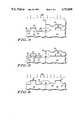
- FIGS. 1-7illustrate, in cross-section, process steps in accordance with one embodiment of the invention for fabricating single LDD CMOS structures
- FIGS. 1-5 and 8-10illustrate, in cross-section, process steps in accordance with a further embodiment of the invention for fabricating double LDD CMOS structures.
- FIGS. 1-7illustrate, in cross-section, process steps for fabricating LDD CMOS structures in accordance with one embodiment of the invention.
- the figuresillustrate the fabrication of one N-channel transistor and one P-channel transistor.
- the processwould provide for the simultaneous fabrication of a number of transistors of each device type as required by the circuit being implemented.
- the process illustratedis a "twin well" process, but the invention is equally applicable to an N-well or to a P-well process.
- FIG. 1illustrates a portion of a silicon substrate 20 which includes a P-type surface region 22 and an N-type surface region 24.
- a thick field oxide 26provides isolation between devices to be formed in N and P-type surface regions, respectively.
- Overlying P-type region 22is a thin insulator 28 which is preferrably silicon dioxide of about 25 nm thickness.
- a thin insulator 30 of the same thicknessis formed on the surface of N-type region 24.
- Gate electrodes 32,34are formed overlying the respective insulators 28,30. Gate electrodes 32,34 are preferrably polycrystalline silicon doped with a conductivity determining impurity to increase the conductivity thereof, but may also be other refractory materials, silicides, polycides and the like.
- a barrier layer 36overlies the surfaces of the electrodes. If the gate electrodes are formed from polycrystalline silicon, barrier layer 36 is preferrably silicon dioxide formed to a thickness of about 30 nm by the thermal oxidation of the polycrystalline silicon.
- a spacer forming material 38is conformally deposited over the surface of the structure.
- the spacer forming materialoverlies the gate electrodes, barrier layers 36, and each of the doped surface regions.
- the spacer forming material 38is preferrably undoped polycrystalline silicon, but other refractory materials such as oxides, nitrides, tungsten, or the like can also be used.
- the thickness of the spacer forming materialdetermines the spacing of the heavily doped source/drain from the gate electrode, and can have a thickness, for example, of about 250 nm.
- the spacer forming materialis readily oxidizable as is polycrystalline silicon, it is preferred that an additional barrier layer 40 is formed over the top surface of the spacer forming material.
- the second barrier layercan be, for example, a layer of chemically vapor deposited silicon nitride with a thickness of about 20 nm.
- conformallymeans that the spacer forming material is deposited with substantially uniform thickness over the surface of the device structure.
- a mask 42such as a layer of patterned photoresist or other resist material overlying N-type surface region 24 as illustrated in FIG. 2.
- Mask 42serves as an etch mask for the selective removal of barrier layer 40 and for the anisotropic etching of spacer forming material 38.
- Mask 42generally covers the N-type surface region while spacers are formed for the fabrication of N-channel devices in the P-type surface region.
- the formation of mask 42is the only lithography step required in the formation of sidewall spacers for the LDD structures in accordance with the invention.
- the exposed portion of the spacer forming material 38is anisotropically etched, for example by reactive ion etching.
- the nature of the anisotropic etching of the conformal layer 38results in the formation of spacers 44 at the edges of gate electrode 32.
- Insulator layer 28protects the surface of surface region 22 and first barrier layer 36 protects the gate electrode 32 at the end of the anisotropic etch step. Layers 28,36 thus act as etch stops for the anisotropic etching.
- barrier layer 40 and spacer forming material 38are sequentially etched in a single etching operation.
- silicon nitride and polycrystalline siliconcan be reactive ion etched in a chlorine based chemistry. If the etchants further include constituents for sidewall passivation such as HBr, the polycrystalline silicon is etched more than 50 times faster than the silicon dioxide layers 28 and 36.
- the structureis ion implanted with an N-type dopant such as arsenic at an energy of 80 keV to a dose of 7 ⁇ 10 15 cm -2 to form the heavily doped portion of the source and drain regions of N-channel MOS transistors.
- the implantationis illustrated by arrows 46 and is masked by gate electrode 32, spacers 44, and field oxide 26.
- Mask 42is also preferrably left on the structure to act as an ion implantation mask, but the masking can be done by barrier 40 and sidewall spacer material 38.
- the implantationplaces a quantity of N-type doping material into the surface of P-type region 22 to form a portion 48 of the source and drain regions as illustrated in FIG. 3. Portion 48 is spaced from the gate electrode structure by the width of sidewall spacers 44(and also by the thickness of barrier material 36).
- the lightly doped portions of the source and drain regionsare implanted using the gate electrode 32 as an implantation mask as illustrated in FIG. 4.
- the spacerscan be removed, for example, by an isotropic dry etch such as SF6.
- the implantation of an N-type conductivity determining impurity such as phosphorus or arsenicis illustrated by arrows 50 and causes the introduction of the dopant material into area 52 of the source and drain regions.
- the implantation of the lightly doped portionscan be, for example, ions of phosphorus at 40 keV to a dose of 5 ⁇ 10 13 cm -2 .
- the implantationis of course also masked by mask 42 and field oxide 26. The implantation also overlaps the more heavily doped region 48.
- Mask 42is removed and the structure is heated in an oxidizing ambient to redistribute ("drive-in") the ion implanted material and to grow a thicker oxide 54 over the surface of the P-type surface region 22.
- the redistribution and oxidationare done in a two step heat treatment.
- the structureis first heated to about 900° C. for 30 minutes in an inert ambient and then is oxidized for about 20 minutes at about 830° C. in dilute steam to grow about 90 nm of thermal oxide on the N+silicon.
- the source and drain regions 56have the characteristics illustrated in FIG. 5.
- the source and drain regionshave a lightly doped portion 58 which is aligned with and diffused slightly under the edge of gate electrode 32 and a more heavily doped region 60 which is spaced from the edge of the gate electrode. Whether the heavily doped or lightly doped region is deeper is determined primarily by the diffusion rate of the dopant species used for the two regions. If phosphorus is used for the lightly doped region and arsenic for the heavily doped region, the lightly doped phosphorus region is likely to be deeper.
- barrier layer 40prevents the oxidation of the upper surface of the remainder of spacer forming material 38. The exposed edge of that material is, however, oxidized to form oxide region 62.
- Undoped polycrystalline silicon 38oxidizes more slowly than either N+doped single crystal silicon or N+doped polycrystalline silicon.
- Oxide region 62can thus be removed in dilute HF (e.g. 100:1) without adversely affecting oxide 36 or 54. If spacer forming material 38 is removed before etching oxide region 62, region 62 will be etched from both sides and will be removed even more quickly. Further, the formation of region 62 can be prevented by heat treating the structure, including the exposed edge of polycrystalline silicon 38, in N 2 (for example, in a rapid thermal anneal process) before growing thermal oxide 54. The N 2 treatment will grow a thin layer of silicon nitride on the edge of the polycrystalline silicon which will prevent oxidation.
- N 2for example, in a rapid thermal anneal process
- barrier layer 40can be eliminated from the process, thus allowing the top surface of material 38 to also oxidize during the growth of oxide 54.
- the presence of mask 42 during the implantation stepsprevents the doping of material 38.
- the surface of the source and drain regionsbeing heavily doped with the implanted ions, oxidizes more rapidly than does the top surface of the undoped spacer forming material 38.
- An oxide thickness differentialthus exists between the oxide grown over the source and drain regions and the oxide grown over the spacer forming material.
- barrier layer 40is removed by etching selectively in an etchant which removes the barrier layer substantially faster than oxide 54.
- the barrier layeris silicon nitride, for example, the nitride is etched by a dip in dilute HF (e.g., 100:1) followed by about 30 seconds in hot (160° C.) phosphoric acid.
- Oxide 54is etched very little during the etching of the nitride.
- the spacer forming material 38is then removed, again with a preferential etchant which does not substantially affect oxide 54.
- Polycrystalline siliconfor example, is plasma etched in a chlorine chemistry containing Cl 2 and HBr followed by a short isotropic clean up etch in SF 6 which etches oxide 54 relatively slowly.
- the structureis then implanted with a P-type conductivity determining impurity to dope the source and drain regions of the P-channel transistors which are to be formed.
- the implantationas illustrated by arrows 64 places the P-type dopant into selected regions 66 of N-doped surface region 24 in self-alignment with gate electrode 34.
- the ion implantation 64is masked by the field oxide 26 and gate electrodes 32 and 34 as well as by the oxide 54 grown over the N-type source and drain regions.
- the implantationcan be done with BF2 ions at an energy of 65 keV and a dose of 5 ⁇ 10 15 cm -2 .
- the source and drain structure of the P-channel devicesis then completed by a thermal redistribution of the P-type implanted dopant material to form source and drain regions 68 as illustrated in FIG. 7.
- the redistributioncan be done, for example, at 900° C. for 15 minutes.
- This redistribution stepis independent of the redistribution of the source and drain regions of the N-channel devices except that it is, of course, cumulative in effect to the thermal redistribution already performed on those regions.
- the LDD structureis formed only on the N-channel devices and the P-channel devices have a conventional, non-LDD structure. The processing of such a structure then continues in a conventional manner to produce the necessary insulators, contact metallization, and the like.
- FIGS. 8-10An alternate embodiment of the invention is illustrated in FIGS. 8-10 which illustrate a continuation of a process after the structure derived in FIG. 5 has been achieved.
- This embodiment of the inventionthus includes the steps shown in FIGS. 1-5 together with the steps shown in FIGS. 8-10.
- the processcontinues by removing barrier layer 40 and anisotropically etching sidewall forming material 38 to form sidewalls 70 illustrated in FIG. 8.
- This process for forming sidewallsis the same as that described above for forming sidewalls 44 in FIG. 2.
- the structureis implanted with a P-type conductivity determining dopant as illustrated by the arrows 72 to form doped regions 74.
- doped regions 74For example, BF2 ions are implanted at an energy of 65 keV to a dose of 5 ⁇ 10 14 cm -2 . These doped regions are heavily doped and are spaced laterally away from gate electrode 34 by the thickness of sidewall spacer 70 (and the thickness of barrier layer 36).
- the second implantation of P-type conductivity determining ionsforms a doped region 78 which is more lightly doped than region 74 and which is self-aligned with gate electrode 34.
- the second P-type implantcan be, for example, BF 2 ions at an energy of 65 keV to a dose of 1 ⁇ 10 14 cm -2 .
- the structureis then thermally annealed to redistribute the two P-type ion implantations to form source and drain regions 80 having a deep and heavily doped region 82 which is spaced away from gate electrode 34 and a more lightly doped portion 84 which is aligned with and slightly overlapped by the gate electrode 34.
- the processing of the structure illustrated in FIG. 10continues in conventional manner to provide necessary and conventional insulating layers, contact metallization, and the like.
- the structure illustrated in FIG. 10is provided with a double LDD structure; that is, the LDD structure is found on both the N-channel and P-channel MOS transistors.
Landscapes
- Insulated Gate Type Field-Effect Transistor (AREA)
- Metal-Oxide And Bipolar Metal-Oxide Semiconductor Integrated Circuits (AREA)
Abstract
Description
Claims (14)
Priority Applications (1)
| Application Number | Priority Date | Filing Date | Title |
|---|---|---|---|
| US07/071,002US4753898A (en) | 1987-07-09 | 1987-07-09 | LDD CMOS process |
Applications Claiming Priority (1)
| Application Number | Priority Date | Filing Date | Title |
|---|---|---|---|
| US07/071,002US4753898A (en) | 1987-07-09 | 1987-07-09 | LDD CMOS process |
Publications (1)
| Publication Number | Publication Date |
|---|---|
| US4753898Atrue US4753898A (en) | 1988-06-28 |
Family
ID=22098681
Family Applications (1)
| Application Number | Title | Priority Date | Filing Date |
|---|---|---|---|
| US07/071,002Expired - LifetimeUS4753898A (en) | 1987-07-09 | 1987-07-09 | LDD CMOS process |
Country Status (1)
| Country | Link |
|---|---|
| US (1) | US4753898A (en) |
Cited By (211)
| Publication number | Priority date | Publication date | Assignee | Title |
|---|---|---|---|---|
| US4876213A (en)* | 1988-10-31 | 1989-10-24 | Motorola, Inc. | Salicided source/drain structure |
| US4908327A (en)* | 1988-05-02 | 1990-03-13 | Texas Instruments, Incorporated | Counter-doped transistor |
| US4925807A (en)* | 1988-06-30 | 1990-05-15 | Kabushiki Kaisha Toshiba | Method of manufacturing a semiconductor device |
| US4956311A (en)* | 1989-06-27 | 1990-09-11 | National Semiconductor Corporation | Double-diffused drain CMOS process using a counterdoping technique |
| US4962054A (en)* | 1988-04-11 | 1990-10-09 | Sumitomo Electric Industries, Ltd. | Method for manufacturing a field effect transistor using spacers of different thicknesses |
| EP0403368A1 (en)* | 1989-06-14 | 1990-12-19 | Commissariat A L'energie Atomique | Method of fabricating an integrated circuit with a double implanted field-effect transistor |
| US4997782A (en)* | 1988-08-04 | 1991-03-05 | Sgs-Thomson Microelectronics S.R.L. | Fabrication of CMOS integrated devices with reduced gate length and lightly doped drain |
| WO1991004577A1 (en)* | 1989-09-22 | 1991-04-04 | Board Of Regents, The University Of Texas System | Hot-carrier suppressed sub-micron misfet device |
| US5013675A (en)* | 1989-05-23 | 1991-05-07 | Advanced Micro Devices, Inc. | Method of forming and removing polysilicon lightly doped drain spacers |
| US5015595A (en)* | 1988-09-09 | 1991-05-14 | Advanced Micro Devices, Inc. | Method of making a high performance MOS device having both P- and N-LDD regions using single photoresist mask |
| US5024959A (en)* | 1989-09-25 | 1991-06-18 | Motorola, Inc. | CMOS process using doped glass layer |
| US5032530A (en)* | 1989-10-27 | 1991-07-16 | Micron Technology, Inc. | Split-polysilicon CMOS process incorporating unmasked punchthrough and source/drain implants |
| US5036019A (en)* | 1989-06-16 | 1991-07-30 | Nippondenso Co., Ltd. | Method of producing a complementary-type semiconductor device |
| US5093275A (en)* | 1989-09-22 | 1992-03-03 | The Board Of Regents, The University Of Texas System | Method for forming hot-carrier suppressed sub-micron MISFET device |
| US5102816A (en)* | 1990-03-27 | 1992-04-07 | Sematech, Inc. | Staircase sidewall spacer for improved source/drain architecture |
| US5141890A (en)* | 1982-02-01 | 1992-08-25 | Texas Instruments Incorporated | CMOS sidewall oxide-lightly doped drain process |
| US5212105A (en)* | 1989-05-24 | 1993-05-18 | Kabushiki Kaisha Toshiba | Semiconductor device manufacturing method and semiconductor device manufactured thereby |
| US5215936A (en)* | 1986-10-09 | 1993-06-01 | Kabushiki Kaisha Toshiba | Method of fabricating a semiconductor device having a lightly-doped drain structure |
| US5238859A (en)* | 1988-04-26 | 1993-08-24 | Kabushiki Kaisha Toshiba | Method of manufacturing semiconductor device |
| US5262344A (en)* | 1990-04-27 | 1993-11-16 | Digital Equipment Corporation | N-channel clamp for ESD protection in self-aligned silicided CMOS process |
| US5270233A (en)* | 1991-06-25 | 1993-12-14 | Nec Corporation | Method for manufacturing field effect transistor having LDD structure |
| US5399513A (en)* | 1989-06-27 | 1995-03-21 | National Semiconductor Corporation | Salicide compatible CMOS process with a differential oxide implant mask |
| US5399514A (en)* | 1990-04-24 | 1995-03-21 | Seiko Epson Corporation | Method for manufacturing improved lightly doped diffusion (LDD) semiconductor device |
| US5405791A (en)* | 1994-10-04 | 1995-04-11 | Micron Semiconductor, Inc. | Process for fabricating ULSI CMOS circuits using a single polysilicon gate layer and disposable spacers |
| BE1007221A3 (en)* | 1993-06-15 | 1995-04-25 | Philips Electronics Nv | METHOD FOR MANUFACTURING A SEMICONDUCTOR DEVICE |
| US5416036A (en)* | 1993-10-04 | 1995-05-16 | United Microelectronics Corporation | Method of improvement ESD for LDD process |
| US5472890A (en)* | 1994-04-28 | 1995-12-05 | Nec Corporation | Method for fabricating an insulating gate field effect transistor |
| US5534449A (en)* | 1995-07-17 | 1996-07-09 | Micron Technology, Inc. | Methods of forming complementary metal oxide semiconductor (CMOS) integrated circuitry |
| US5580805A (en)* | 1993-09-10 | 1996-12-03 | Sony Corporation | Semiconductor device having various threshold voltages and manufacturing same |
| US5585299A (en)* | 1996-03-19 | 1996-12-17 | United Microelectronics Corporation | Process for fabricating a semiconductor electrostatic discharge (ESD) protective device |
| US5595918A (en)* | 1995-03-23 | 1997-01-21 | International Rectifier Corporation | Process for manufacture of P channel MOS-gated device |
| US5635413A (en)* | 1992-08-03 | 1997-06-03 | Mitsubishi Denki Kabushiki Kaisha | Method of manufacturing field effect transistor |
| US5654213A (en)* | 1995-10-03 | 1997-08-05 | Integrated Device Technology, Inc. | Method for fabricating a CMOS device |
| US5693505A (en)* | 1993-12-24 | 1997-12-02 | Nec Corporation | Method of fabricating a semiconductor device |
| US5698463A (en)* | 1995-05-29 | 1997-12-16 | Yamaha Corporation | Semiconductor IC with FET and capacitor having side wall spacers and manufacturing method thereof |
| US5733818A (en)* | 1995-10-18 | 1998-03-31 | Nec Corporation | Method for fabricating semiconductor device with planarization step using CMP |
| US5766991A (en)* | 1990-05-11 | 1998-06-16 | U.S. Philips Corporation | CMOS process utilizing disposable silicon nitride spacers for making lightly doped drain |
| US5841164A (en)* | 1995-10-30 | 1998-11-24 | Mitsubishi Denki Kabushiki Kaisha | Test structure for dielectric film evaluation |
| US5869377A (en)* | 1984-08-22 | 1999-02-09 | Mitsubishi Denki Kabushiki Kaisha | Method of fabrication LDD semiconductor device with amorphous regions |
| US5904509A (en)* | 1994-01-08 | 1999-05-18 | Semiconductor Energy Laboratory Co., Ltd. | Method of manufacturing a thin film transistor using anodic oxidation |
| US5925913A (en)* | 1997-08-25 | 1999-07-20 | Advanced Micro Devices, Inc. | System for enhancing the performance of a circuit by reducing the channel length of one or more transistors |
| US6004854A (en)* | 1995-07-17 | 1999-12-21 | Micron Technology, Inc. | Method of forming CMOS integrated circuitry |
| US6020232A (en)* | 1996-12-03 | 2000-02-01 | Advanced Micro Devices, Inc. | Process of fabricating transistors having source and drain regions laterally displaced from the transistors gate |
| US6043128A (en)* | 1997-02-07 | 2000-03-28 | Yamaha Corporation | Semiconductor device handling multi-level voltages |
| US6071767A (en)* | 1991-01-18 | 2000-06-06 | International Business Machines Corporation | High performance/high density BICMOS process |
| US6121090A (en)* | 1998-04-20 | 2000-09-19 | Texas Instruments - Acer Incorporated | Self-aligned silicided MOS devices with an extended S/D junction and an ESD protection circuit |
| US6232209B1 (en)* | 1999-06-11 | 2001-05-15 | Mitsubishi Denki Kabushiki Kaisha | Semiconductor device and manufacturing method thereof |
| US6245624B1 (en)* | 1998-07-24 | 2001-06-12 | Samsung Electronics Co., Ltd. | Methods of fabricating field effect transistors by first forming heavily doped source/drain regions and then forming lightly doped source/drain regions |
| US6258646B1 (en)* | 1996-12-06 | 2001-07-10 | Advanced Micro Devices, Inc. | CMOS integrated circuit and method for implanting NMOS transistor areas prior to implanting PMOS transistor areas to optimize the thermal diffusivity thereof |
| US6455362B1 (en)* | 2000-08-22 | 2002-09-24 | Micron Technology, Inc. | Double LDD devices for improved dram refresh |
| US20030162343A1 (en)* | 2002-02-26 | 2003-08-28 | Altmann Michael W. | Physically defined varactor in a CMOS process |
| US20040056304A1 (en)* | 2002-09-19 | 2004-03-25 | Shafqat Ahmed | Method of forming transistor having insulating spacers on gate sidewalls |
| US20060051966A1 (en)* | 2004-02-26 | 2006-03-09 | Applied Materials, Inc. | In-situ chamber clean process to remove by-product deposits from chemical vapor etch chamber |
| US20060054979A1 (en)* | 2003-12-12 | 2006-03-16 | Philipp Kratzert | Method for fabricating a drain/source path |
| US20070155109A1 (en)* | 2005-12-29 | 2007-07-05 | Hyun Soo Shin | Method for fabricating a semiconductor device |
| US20070202640A1 (en)* | 2006-02-28 | 2007-08-30 | Applied Materials, Inc. | Low-k spacer integration into CMOS transistors |
| US20070281415A1 (en)* | 2003-09-03 | 2007-12-06 | Semiconductor Technology Academic Research Center | Semiconductor device and manufacturing method thereof |
| US20090095621A1 (en)* | 2004-02-26 | 2009-04-16 | Chien-Teh Kao | Support assembly |
| US20090215991A1 (en)* | 2003-03-03 | 2009-08-27 | Xencor, Inc. | Optimized Fc Variants and methods for their generation |
| CN101834193A (en)* | 2009-03-12 | 2010-09-15 | 索尼公司 | Method for manufacturing solid-state image pickup device |
| US20110124173A1 (en)* | 2009-11-25 | 2011-05-26 | Sung-Hwan Kim | Method of Manufacturing Semiconductor Device |
| US8679982B2 (en) | 2011-08-26 | 2014-03-25 | Applied Materials, Inc. | Selective suppression of dry-etch rate of materials containing both silicon and oxygen |
| US8679983B2 (en) | 2011-09-01 | 2014-03-25 | Applied Materials, Inc. | Selective suppression of dry-etch rate of materials containing both silicon and nitrogen |
| US8765574B2 (en) | 2012-11-09 | 2014-07-01 | Applied Materials, Inc. | Dry etch process |
| US8771539B2 (en) | 2011-02-22 | 2014-07-08 | Applied Materials, Inc. | Remotely-excited fluorine and water vapor etch |
| US8801952B1 (en) | 2013-03-07 | 2014-08-12 | Applied Materials, Inc. | Conformal oxide dry etch |
| US8808563B2 (en) | 2011-10-07 | 2014-08-19 | Applied Materials, Inc. | Selective etch of silicon by way of metastable hydrogen termination |
| US8895449B1 (en) | 2013-05-16 | 2014-11-25 | Applied Materials, Inc. | Delicate dry clean |
| US8921234B2 (en) | 2012-12-21 | 2014-12-30 | Applied Materials, Inc. | Selective titanium nitride etching |
| US8927390B2 (en) | 2011-09-26 | 2015-01-06 | Applied Materials, Inc. | Intrench profile |
| US8951429B1 (en) | 2013-10-29 | 2015-02-10 | Applied Materials, Inc. | Tungsten oxide processing |
| US8956980B1 (en) | 2013-09-16 | 2015-02-17 | Applied Materials, Inc. | Selective etch of silicon nitride |
| US8969212B2 (en) | 2012-11-20 | 2015-03-03 | Applied Materials, Inc. | Dry-etch selectivity |
| US8975152B2 (en) | 2011-11-08 | 2015-03-10 | Applied Materials, Inc. | Methods of reducing substrate dislocation during gapfill processing |
| US8980763B2 (en) | 2012-11-30 | 2015-03-17 | Applied Materials, Inc. | Dry-etch for selective tungsten removal |
| US8999856B2 (en) | 2011-03-14 | 2015-04-07 | Applied Materials, Inc. | Methods for etch of sin films |
| US9023732B2 (en) | 2013-03-15 | 2015-05-05 | Applied Materials, Inc. | Processing systems and methods for halide scavenging |
| US9023734B2 (en) | 2012-09-18 | 2015-05-05 | Applied Materials, Inc. | Radical-component oxide etch |
| US9034770B2 (en) | 2012-09-17 | 2015-05-19 | Applied Materials, Inc. | Differential silicon oxide etch |
| US9040422B2 (en) | 2013-03-05 | 2015-05-26 | Applied Materials, Inc. | Selective titanium nitride removal |
| US9064816B2 (en) | 2012-11-30 | 2015-06-23 | Applied Materials, Inc. | Dry-etch for selective oxidation removal |
| US9064815B2 (en) | 2011-03-14 | 2015-06-23 | Applied Materials, Inc. | Methods for etch of metal and metal-oxide films |
| US9111877B2 (en) | 2012-12-18 | 2015-08-18 | Applied Materials, Inc. | Non-local plasma oxide etch |
| US9114438B2 (en) | 2013-05-21 | 2015-08-25 | Applied Materials, Inc. | Copper residue chamber clean |
| US9117855B2 (en) | 2013-12-04 | 2015-08-25 | Applied Materials, Inc. | Polarity control for remote plasma |
| US9136273B1 (en) | 2014-03-21 | 2015-09-15 | Applied Materials, Inc. | Flash gate air gap |
| US9132436B2 (en) | 2012-09-21 | 2015-09-15 | Applied Materials, Inc. | Chemical control features in wafer process equipment |
| US9159606B1 (en) | 2014-07-31 | 2015-10-13 | Applied Materials, Inc. | Metal air gap |
| US9165786B1 (en) | 2014-08-05 | 2015-10-20 | Applied Materials, Inc. | Integrated oxide and nitride recess for better channel contact in 3D architectures |
| US9190293B2 (en) | 2013-12-18 | 2015-11-17 | Applied Materials, Inc. | Even tungsten etch for high aspect ratio trenches |
| US9236265B2 (en) | 2013-11-04 | 2016-01-12 | Applied Materials, Inc. | Silicon germanium processing |
| US9236266B2 (en) | 2011-08-01 | 2016-01-12 | Applied Materials, Inc. | Dry-etch for silicon-and-carbon-containing films |
| US9245762B2 (en) | 2013-12-02 | 2016-01-26 | Applied Materials, Inc. | Procedure for etch rate consistency |
| US9263278B2 (en) | 2013-12-17 | 2016-02-16 | Applied Materials, Inc. | Dopant etch selectivity control |
| US9269590B2 (en) | 2014-04-07 | 2016-02-23 | Applied Materials, Inc. | Spacer formation |
| US9287095B2 (en) | 2013-12-17 | 2016-03-15 | Applied Materials, Inc. | Semiconductor system assemblies and methods of operation |
| US9287134B2 (en) | 2014-01-17 | 2016-03-15 | Applied Materials, Inc. | Titanium oxide etch |
| US9293568B2 (en) | 2014-01-27 | 2016-03-22 | Applied Materials, Inc. | Method of fin patterning |
| US9299537B2 (en) | 2014-03-20 | 2016-03-29 | Applied Materials, Inc. | Radial waveguide systems and methods for post-match control of microwaves |
| US9299575B2 (en) | 2014-03-17 | 2016-03-29 | Applied Materials, Inc. | Gas-phase tungsten etch |
| US9299583B1 (en) | 2014-12-05 | 2016-03-29 | Applied Materials, Inc. | Aluminum oxide selective etch |
| US9299538B2 (en) | 2014-03-20 | 2016-03-29 | Applied Materials, Inc. | Radial waveguide systems and methods for post-match control of microwaves |
| US9299582B2 (en) | 2013-11-12 | 2016-03-29 | Applied Materials, Inc. | Selective etch for metal-containing materials |
| US9309598B2 (en) | 2014-05-28 | 2016-04-12 | Applied Materials, Inc. | Oxide and metal removal |
| US9324576B2 (en) | 2010-05-27 | 2016-04-26 | Applied Materials, Inc. | Selective etch for silicon films |
| US9343272B1 (en) | 2015-01-08 | 2016-05-17 | Applied Materials, Inc. | Self-aligned process |
| US9349605B1 (en) | 2015-08-07 | 2016-05-24 | Applied Materials, Inc. | Oxide etch selectivity systems and methods |
| US9355856B2 (en) | 2014-09-12 | 2016-05-31 | Applied Materials, Inc. | V trench dry etch |
| US9355862B2 (en) | 2014-09-24 | 2016-05-31 | Applied Materials, Inc. | Fluorine-based hardmask removal |
| US9362130B2 (en) | 2013-03-01 | 2016-06-07 | Applied Materials, Inc. | Enhanced etching processes using remote plasma sources |
| US9368364B2 (en) | 2014-09-24 | 2016-06-14 | Applied Materials, Inc. | Silicon etch process with tunable selectivity to SiO2 and other materials |
| US9373522B1 (en) | 2015-01-22 | 2016-06-21 | Applied Mateials, Inc. | Titanium nitride removal |
| US9373517B2 (en) | 2012-08-02 | 2016-06-21 | Applied Materials, Inc. | Semiconductor processing with DC assisted RF power for improved control |
| US9378969B2 (en) | 2014-06-19 | 2016-06-28 | Applied Materials, Inc. | Low temperature gas-phase carbon removal |
| US9378978B2 (en) | 2014-07-31 | 2016-06-28 | Applied Materials, Inc. | Integrated oxide recess and floating gate fin trimming |
| US9385028B2 (en) | 2014-02-03 | 2016-07-05 | Applied Materials, Inc. | Air gap process |
| US9390937B2 (en) | 2012-09-20 | 2016-07-12 | Applied Materials, Inc. | Silicon-carbon-nitride selective etch |
| US9396989B2 (en) | 2014-01-27 | 2016-07-19 | Applied Materials, Inc. | Air gaps between copper lines |
| US9406523B2 (en) | 2014-06-19 | 2016-08-02 | Applied Materials, Inc. | Highly selective doped oxide removal method |
| US9425058B2 (en) | 2014-07-24 | 2016-08-23 | Applied Materials, Inc. | Simplified litho-etch-litho-etch process |
| US9449846B2 (en) | 2015-01-28 | 2016-09-20 | Applied Materials, Inc. | Vertical gate separation |
| US9478432B2 (en) | 2014-09-25 | 2016-10-25 | Applied Materials, Inc. | Silicon oxide selective removal |
| US9493879B2 (en) | 2013-07-12 | 2016-11-15 | Applied Materials, Inc. | Selective sputtering for pattern transfer |
| US9496167B2 (en) | 2014-07-31 | 2016-11-15 | Applied Materials, Inc. | Integrated bit-line airgap formation and gate stack post clean |
| US9499898B2 (en) | 2014-03-03 | 2016-11-22 | Applied Materials, Inc. | Layered thin film heater and method of fabrication |
| US9502258B2 (en) | 2014-12-23 | 2016-11-22 | Applied Materials, Inc. | Anisotropic gap etch |
| US9553102B2 (en) | 2014-08-19 | 2017-01-24 | Applied Materials, Inc. | Tungsten separation |
| US9576809B2 (en) | 2013-11-04 | 2017-02-21 | Applied Materials, Inc. | Etch suppression with germanium |
| US9659753B2 (en) | 2014-08-07 | 2017-05-23 | Applied Materials, Inc. | Grooved insulator to reduce leakage current |
| US9691645B2 (en) | 2015-08-06 | 2017-06-27 | Applied Materials, Inc. | Bolted wafer chuck thermal management systems and methods for wafer processing systems |
| US9721789B1 (en) | 2016-10-04 | 2017-08-01 | Applied Materials, Inc. | Saving ion-damaged spacers |
| US9728437B2 (en) | 2015-02-03 | 2017-08-08 | Applied Materials, Inc. | High temperature chuck for plasma processing systems |
| US9741593B2 (en) | 2015-08-06 | 2017-08-22 | Applied Materials, Inc. | Thermal management systems and methods for wafer processing systems |
| US9768034B1 (en) | 2016-11-11 | 2017-09-19 | Applied Materials, Inc. | Removal methods for high aspect ratio structures |
| US9773648B2 (en) | 2013-08-30 | 2017-09-26 | Applied Materials, Inc. | Dual discharge modes operation for remote plasma |
| US9847289B2 (en) | 2014-05-30 | 2017-12-19 | Applied Materials, Inc. | Protective via cap for improved interconnect performance |
| US9865484B1 (en) | 2016-06-29 | 2018-01-09 | Applied Materials, Inc. | Selective etch using material modification and RF pulsing |
| US9881805B2 (en) | 2015-03-02 | 2018-01-30 | Applied Materials, Inc. | Silicon selective removal |
| US9885117B2 (en) | 2014-03-31 | 2018-02-06 | Applied Materials, Inc. | Conditioned semiconductor system parts |
| US9934942B1 (en) | 2016-10-04 | 2018-04-03 | Applied Materials, Inc. | Chamber with flow-through source |
| US9947549B1 (en) | 2016-10-10 | 2018-04-17 | Applied Materials, Inc. | Cobalt-containing material removal |
| US10026621B2 (en) | 2016-11-14 | 2018-07-17 | Applied Materials, Inc. | SiN spacer profile patterning |
| US10043684B1 (en) | 2017-02-06 | 2018-08-07 | Applied Materials, Inc. | Self-limiting atomic thermal etching systems and methods |
| US10043674B1 (en) | 2017-08-04 | 2018-08-07 | Applied Materials, Inc. | Germanium etching systems and methods |
| US10049891B1 (en) | 2017-05-31 | 2018-08-14 | Applied Materials, Inc. | Selective in situ cobalt residue removal |
| US10062585B2 (en) | 2016-10-04 | 2018-08-28 | Applied Materials, Inc. | Oxygen compatible plasma source |
| US10062587B2 (en) | 2012-07-18 | 2018-08-28 | Applied Materials, Inc. | Pedestal with multi-zone temperature control and multiple purge capabilities |
| US10062575B2 (en) | 2016-09-09 | 2018-08-28 | Applied Materials, Inc. | Poly directional etch by oxidation |
| US10062579B2 (en) | 2016-10-07 | 2018-08-28 | Applied Materials, Inc. | Selective SiN lateral recess |
| US10128086B1 (en) | 2017-10-24 | 2018-11-13 | Applied Materials, Inc. | Silicon pretreatment for nitride removal |
| US10163696B2 (en) | 2016-11-11 | 2018-12-25 | Applied Materials, Inc. | Selective cobalt removal for bottom up gapfill |
| US10170282B2 (en) | 2013-03-08 | 2019-01-01 | Applied Materials, Inc. | Insulated semiconductor faceplate designs |
| US10170336B1 (en) | 2017-08-04 | 2019-01-01 | Applied Materials, Inc. | Methods for anisotropic control of selective silicon removal |
| US10224210B2 (en) | 2014-12-09 | 2019-03-05 | Applied Materials, Inc. | Plasma processing system with direct outlet toroidal plasma source |
| US10242908B2 (en) | 2016-11-14 | 2019-03-26 | Applied Materials, Inc. | Airgap formation with damage-free copper |
| US10256079B2 (en) | 2013-02-08 | 2019-04-09 | Applied Materials, Inc. | Semiconductor processing systems having multiple plasma configurations |
| US10256112B1 (en) | 2017-12-08 | 2019-04-09 | Applied Materials, Inc. | Selective tungsten removal |
| US10283324B1 (en) | 2017-10-24 | 2019-05-07 | Applied Materials, Inc. | Oxygen treatment for nitride etching |
| US10283321B2 (en) | 2011-01-18 | 2019-05-07 | Applied Materials, Inc. | Semiconductor processing system and methods using capacitively coupled plasma |
| US10297458B2 (en) | 2017-08-07 | 2019-05-21 | Applied Materials, Inc. | Process window widening using coated parts in plasma etch processes |
| US10319649B2 (en) | 2017-04-11 | 2019-06-11 | Applied Materials, Inc. | Optical emission spectroscopy (OES) for remote plasma monitoring |
| US10319600B1 (en) | 2018-03-12 | 2019-06-11 | Applied Materials, Inc. | Thermal silicon etch |
| US10319739B2 (en) | 2017-02-08 | 2019-06-11 | Applied Materials, Inc. | Accommodating imperfectly aligned memory holes |
| US10354889B2 (en) | 2017-07-17 | 2019-07-16 | Applied Materials, Inc. | Non-halogen etching of silicon-containing materials |
| US10403507B2 (en) | 2017-02-03 | 2019-09-03 | Applied Materials, Inc. | Shaped etch profile with oxidation |
| US10431429B2 (en) | 2017-02-03 | 2019-10-01 | Applied Materials, Inc. | Systems and methods for radial and azimuthal control of plasma uniformity |
| US10468267B2 (en) | 2017-05-31 | 2019-11-05 | Applied Materials, Inc. | Water-free etching methods |
| US10490418B2 (en) | 2014-10-14 | 2019-11-26 | Applied Materials, Inc. | Systems and methods for internal surface conditioning assessment in plasma processing equipment |
| US10490406B2 (en) | 2018-04-10 | 2019-11-26 | Appled Materials, Inc. | Systems and methods for material breakthrough |
| US10497573B2 (en) | 2018-03-13 | 2019-12-03 | Applied Materials, Inc. | Selective atomic layer etching of semiconductor materials |
| US10504754B2 (en) | 2016-05-19 | 2019-12-10 | Applied Materials, Inc. | Systems and methods for improved semiconductor etching and component protection |
| US10504700B2 (en) | 2015-08-27 | 2019-12-10 | Applied Materials, Inc. | Plasma etching systems and methods with secondary plasma injection |
| US10522371B2 (en) | 2016-05-19 | 2019-12-31 | Applied Materials, Inc. | Systems and methods for improved semiconductor etching and component protection |
| US10541184B2 (en) | 2017-07-11 | 2020-01-21 | Applied Materials, Inc. | Optical emission spectroscopic techniques for monitoring etching |
| US10541246B2 (en) | 2017-06-26 | 2020-01-21 | Applied Materials, Inc. | 3D flash memory cells which discourage cross-cell electrical tunneling |
| US10546729B2 (en) | 2016-10-04 | 2020-01-28 | Applied Materials, Inc. | Dual-channel showerhead with improved profile |
| US10566206B2 (en) | 2016-12-27 | 2020-02-18 | Applied Materials, Inc. | Systems and methods for anisotropic material breakthrough |
| US10573527B2 (en) | 2018-04-06 | 2020-02-25 | Applied Materials, Inc. | Gas-phase selective etching systems and methods |
| US10573496B2 (en) | 2014-12-09 | 2020-02-25 | Applied Materials, Inc. | Direct outlet toroidal plasma source |
| US10593560B2 (en) | 2018-03-01 | 2020-03-17 | Applied Materials, Inc. | Magnetic induction plasma source for semiconductor processes and equipment |
| US10593523B2 (en) | 2014-10-14 | 2020-03-17 | Applied Materials, Inc. | Systems and methods for internal surface conditioning in plasma processing equipment |
| US10615047B2 (en) | 2018-02-28 | 2020-04-07 | Applied Materials, Inc. | Systems and methods to form airgaps |
| US10629473B2 (en) | 2016-09-09 | 2020-04-21 | Applied Materials, Inc. | Footing removal for nitride spacer |
| US10672642B2 (en) | 2018-07-24 | 2020-06-02 | Applied Materials, Inc. | Systems and methods for pedestal configuration |
| US10679870B2 (en) | 2018-02-15 | 2020-06-09 | Applied Materials, Inc. | Semiconductor processing chamber multistage mixing apparatus |
| US10699879B2 (en) | 2018-04-17 | 2020-06-30 | Applied Materials, Inc. | Two piece electrode assembly with gap for plasma control |
| US10727080B2 (en) | 2017-07-07 | 2020-07-28 | Applied Materials, Inc. | Tantalum-containing material removal |
| US10755941B2 (en) | 2018-07-06 | 2020-08-25 | Applied Materials, Inc. | Self-limiting selective etching systems and methods |
| US10854426B2 (en) | 2018-01-08 | 2020-12-01 | Applied Materials, Inc. | Metal recess for semiconductor structures |
| US10872778B2 (en) | 2018-07-06 | 2020-12-22 | Applied Materials, Inc. | Systems and methods utilizing solid-phase etchants |
| US10886137B2 (en) | 2018-04-30 | 2021-01-05 | Applied Materials, Inc. | Selective nitride removal |
| US10892198B2 (en) | 2018-09-14 | 2021-01-12 | Applied Materials, Inc. | Systems and methods for improved performance in semiconductor processing |
| US10903054B2 (en) | 2017-12-19 | 2021-01-26 | Applied Materials, Inc. | Multi-zone gas distribution systems and methods |
| US10920320B2 (en) | 2017-06-16 | 2021-02-16 | Applied Materials, Inc. | Plasma health determination in semiconductor substrate processing reactors |
| US10920319B2 (en) | 2019-01-11 | 2021-02-16 | Applied Materials, Inc. | Ceramic showerheads with conductive electrodes |
| US10943834B2 (en) | 2017-03-13 | 2021-03-09 | Applied Materials, Inc. | Replacement contact process |
| US10964512B2 (en) | 2018-02-15 | 2021-03-30 | Applied Materials, Inc. | Semiconductor processing chamber multistage mixing apparatus and methods |
| US11049755B2 (en) | 2018-09-14 | 2021-06-29 | Applied Materials, Inc. | Semiconductor substrate supports with embedded RF shield |
| US11062887B2 (en) | 2018-09-17 | 2021-07-13 | Applied Materials, Inc. | High temperature RF heater pedestals |
| US11121002B2 (en) | 2018-10-24 | 2021-09-14 | Applied Materials, Inc. | Systems and methods for etching metals and metal derivatives |
| US11239061B2 (en) | 2014-11-26 | 2022-02-01 | Applied Materials, Inc. | Methods and systems to enhance process uniformity |
| US11257693B2 (en) | 2015-01-09 | 2022-02-22 | Applied Materials, Inc. | Methods and systems to improve pedestal temperature control |
| US11276559B2 (en) | 2017-05-17 | 2022-03-15 | Applied Materials, Inc. | Semiconductor processing chamber for multiple precursor flow |
| US11276590B2 (en) | 2017-05-17 | 2022-03-15 | Applied Materials, Inc. | Multi-zone semiconductor substrate supports |
| US11328909B2 (en) | 2017-12-22 | 2022-05-10 | Applied Materials, Inc. | Chamber conditioning and removal processes |
| US11417534B2 (en) | 2018-09-21 | 2022-08-16 | Applied Materials, Inc. | Selective material removal |
| US11437242B2 (en) | 2018-11-27 | 2022-09-06 | Applied Materials, Inc. | Selective removal of silicon-containing materials |
| US11594428B2 (en) | 2015-02-03 | 2023-02-28 | Applied Materials, Inc. | Low temperature chuck for plasma processing systems |
| US11682560B2 (en) | 2018-10-11 | 2023-06-20 | Applied Materials, Inc. | Systems and methods for hafnium-containing film removal |
| US11721527B2 (en) | 2019-01-07 | 2023-08-08 | Applied Materials, Inc. | Processing chamber mixing systems |
| US12340979B2 (en) | 2017-05-17 | 2025-06-24 | Applied Materials, Inc. | Semiconductor processing chamber for improved precursor flow |
Citations (9)
| Publication number | Priority date | Publication date | Assignee | Title |
|---|---|---|---|---|
| US4350150A (en)* | 1979-09-25 | 1982-09-21 | Olympus Optical Co., Ltd. | Structure of a light-receiving end portion of an endoscope light guide |
| US4356623A (en)* | 1980-09-15 | 1982-11-02 | Texas Instruments Incorporated | Fabrication of submicron semiconductor devices |
| US4382827A (en)* | 1981-04-27 | 1983-05-10 | Ncr Corporation | Silicon nitride S/D ion implant mask in CMOS device fabrication |
| US4433468A (en)* | 1980-03-26 | 1984-02-28 | Nippon Electric Co., Ltd. | Method for making semiconductor device having improved thermal stress characteristics |
| US4488351A (en)* | 1983-01-27 | 1984-12-18 | Tokyo Shibaura Denki Kabushiki Kaisha | Method for manufacturing semiconductor device |
| US4536944A (en)* | 1982-12-29 | 1985-08-27 | International Business Machines Corporation | Method of making ROM/PLA semiconductor device by late stage personalization |
| US4590663A (en)* | 1982-02-01 | 1986-05-27 | Texas Instruments Incorporated | High voltage CMOS technology with N-channel source/drain extensions |
| US4613882A (en)* | 1985-04-12 | 1986-09-23 | General Electric Company | Hybrid extended drain concept for reduced hot electron effect |
| US4642878A (en)* | 1984-08-28 | 1987-02-17 | Kabushiki Kaisha Toshiba | Method of making MOS device by sequentially depositing an oxidizable layer and a masking second layer over gated device regions |
- 1987
- 1987-07-09USUS07/071,002patent/US4753898A/ennot_activeExpired - Lifetime
Patent Citations (10)
| Publication number | Priority date | Publication date | Assignee | Title |
|---|---|---|---|---|
| US4350150A (en)* | 1979-09-25 | 1982-09-21 | Olympus Optical Co., Ltd. | Structure of a light-receiving end portion of an endoscope light guide |
| US4433468A (en)* | 1980-03-26 | 1984-02-28 | Nippon Electric Co., Ltd. | Method for making semiconductor device having improved thermal stress characteristics |
| US4356623A (en)* | 1980-09-15 | 1982-11-02 | Texas Instruments Incorporated | Fabrication of submicron semiconductor devices |
| US4356623B1 (en)* | 1980-09-15 | 1989-07-25 | ||
| US4382827A (en)* | 1981-04-27 | 1983-05-10 | Ncr Corporation | Silicon nitride S/D ion implant mask in CMOS device fabrication |
| US4590663A (en)* | 1982-02-01 | 1986-05-27 | Texas Instruments Incorporated | High voltage CMOS technology with N-channel source/drain extensions |
| US4536944A (en)* | 1982-12-29 | 1985-08-27 | International Business Machines Corporation | Method of making ROM/PLA semiconductor device by late stage personalization |
| US4488351A (en)* | 1983-01-27 | 1984-12-18 | Tokyo Shibaura Denki Kabushiki Kaisha | Method for manufacturing semiconductor device |
| US4642878A (en)* | 1984-08-28 | 1987-02-17 | Kabushiki Kaisha Toshiba | Method of making MOS device by sequentially depositing an oxidizable layer and a masking second layer over gated device regions |
| US4613882A (en)* | 1985-04-12 | 1986-09-23 | General Electric Company | Hybrid extended drain concept for reduced hot electron effect |
Non-Patent Citations (10)
| Title |
|---|
| E. Takeda, et al. "Submicrometer MOSFET Structure for Minimizing Hot-Carrier Generation", IEEE Transactions on Electron Devices, vol. ED-29, No. 4, Apr. 1982, pp. 611-618. |
| E. Takeda, et al. Submicrometer MOSFET Structure for Minimizing Hot Carrier Generation , IEEE Transactions on Electron Devices, vol. ED 29, No. 4, Apr. 1982, pp. 611 618.* |
| Ogura et al., "Latch-up Free, Double-Gated, Enhancement-Type P-Channel Device for CMOS with Enhanced Transconductance", IBM Technical Disclosure Bulletin, vol. 27, No. 1B, Jun. 1984, pp. 722-727. |
| Ogura et al., Latch up Free, Double Gated, Enhancement Type P Channel Device for CMOS with Enhanced Transconductance , IBM Technical Disclosure Bulletin, vol. 27, No. 1B, Jun. 1984, pp. 722 727.* |
| S. Ratham, et al. "An Optimized 0.5 Micron LDD Transistor", International Electron Devices Meeting Papers, vol. 10.2, 1983, pp. 237-241. |
| S. Ratham, et al. An Optimized 0.5 Micron LDD Transistor , International Electron Devices Meeting Papers, vol. 10.2, 1983, pp. 237 241.* |
| Tsang, et al., "Fabrication of High-Performance LDDFET's with Oxide Sidewall-Spacer Technology", IEEE Journal of Solid State Circuits, vol. SC-17, No. 2, Apr. 1987. |
| Tsang, et al., Fabrication of High Performance LDDFET s with Oxide Sidewall Spacer Technology , IEEE Journal of Solid State Circuits, vol. SC 17, No. 2, Apr. 1987.* |
| Y. Matsumoto, et al. "Optimized an Reliable LDD Structure for 1um NMOSFET Based on Substrate Current Analysis", International Electron Devices Meeting Papers, vol. 15.4, 1983, pp. 392-395. |
| Y. Matsumoto, et al. Optimized an Reliable LDD Structure for 1um NMOSFET Based on Substrate Current Analysis , International Electron Devices Meeting Papers, vol. 15.4, 1983, pp. 392 395.* |
Cited By (311)
| Publication number | Priority date | Publication date | Assignee | Title |
|---|---|---|---|---|
| US5141890A (en)* | 1982-02-01 | 1992-08-25 | Texas Instruments Incorporated | CMOS sidewall oxide-lightly doped drain process |
| US5869377A (en)* | 1984-08-22 | 1999-02-09 | Mitsubishi Denki Kabushiki Kaisha | Method of fabrication LDD semiconductor device with amorphous regions |
| US5215936A (en)* | 1986-10-09 | 1993-06-01 | Kabushiki Kaisha Toshiba | Method of fabricating a semiconductor device having a lightly-doped drain structure |
| US4962054A (en)* | 1988-04-11 | 1990-10-09 | Sumitomo Electric Industries, Ltd. | Method for manufacturing a field effect transistor using spacers of different thicknesses |
| US5238859A (en)* | 1988-04-26 | 1993-08-24 | Kabushiki Kaisha Toshiba | Method of manufacturing semiconductor device |
| US4908327A (en)* | 1988-05-02 | 1990-03-13 | Texas Instruments, Incorporated | Counter-doped transistor |
| US4925807A (en)* | 1988-06-30 | 1990-05-15 | Kabushiki Kaisha Toshiba | Method of manufacturing a semiconductor device |
| US4997782A (en)* | 1988-08-04 | 1991-03-05 | Sgs-Thomson Microelectronics S.R.L. | Fabrication of CMOS integrated devices with reduced gate length and lightly doped drain |
| US5015595A (en)* | 1988-09-09 | 1991-05-14 | Advanced Micro Devices, Inc. | Method of making a high performance MOS device having both P- and N-LDD regions using single photoresist mask |
| US4876213A (en)* | 1988-10-31 | 1989-10-24 | Motorola, Inc. | Salicided source/drain structure |
| US5013675A (en)* | 1989-05-23 | 1991-05-07 | Advanced Micro Devices, Inc. | Method of forming and removing polysilicon lightly doped drain spacers |
| US5212105A (en)* | 1989-05-24 | 1993-05-18 | Kabushiki Kaisha Toshiba | Semiconductor device manufacturing method and semiconductor device manufactured thereby |
| EP0403368A1 (en)* | 1989-06-14 | 1990-12-19 | Commissariat A L'energie Atomique | Method of fabricating an integrated circuit with a double implanted field-effect transistor |
| FR2648622A1 (en)* | 1989-06-14 | 1990-12-21 | Commissariat Energie Atomique | METHOD FOR MANUFACTURING AN INTEGRATED CIRCUIT COMPRISING A DUAL IMPLANT FIELD EFFECT TRANSISTOR |
| US5036019A (en)* | 1989-06-16 | 1991-07-30 | Nippondenso Co., Ltd. | Method of producing a complementary-type semiconductor device |
| US4956311A (en)* | 1989-06-27 | 1990-09-11 | National Semiconductor Corporation | Double-diffused drain CMOS process using a counterdoping technique |
| US5399513A (en)* | 1989-06-27 | 1995-03-21 | National Semiconductor Corporation | Salicide compatible CMOS process with a differential oxide implant mask |
| US5093275A (en)* | 1989-09-22 | 1992-03-03 | The Board Of Regents, The University Of Texas System | Method for forming hot-carrier suppressed sub-micron MISFET device |
| WO1991004577A1 (en)* | 1989-09-22 | 1991-04-04 | Board Of Regents, The University Of Texas System | Hot-carrier suppressed sub-micron misfet device |
| US5024959A (en)* | 1989-09-25 | 1991-06-18 | Motorola, Inc. | CMOS process using doped glass layer |
| US5032530A (en)* | 1989-10-27 | 1991-07-16 | Micron Technology, Inc. | Split-polysilicon CMOS process incorporating unmasked punchthrough and source/drain implants |
| US5102816A (en)* | 1990-03-27 | 1992-04-07 | Sematech, Inc. | Staircase sidewall spacer for improved source/drain architecture |
| US5399514A (en)* | 1990-04-24 | 1995-03-21 | Seiko Epson Corporation | Method for manufacturing improved lightly doped diffusion (LDD) semiconductor device |
| US5262344A (en)* | 1990-04-27 | 1993-11-16 | Digital Equipment Corporation | N-channel clamp for ESD protection in self-aligned silicided CMOS process |
| US5766991A (en)* | 1990-05-11 | 1998-06-16 | U.S. Philips Corporation | CMOS process utilizing disposable silicon nitride spacers for making lightly doped drain |
| US6071767A (en)* | 1991-01-18 | 2000-06-06 | International Business Machines Corporation | High performance/high density BICMOS process |
| US5270233A (en)* | 1991-06-25 | 1993-12-14 | Nec Corporation | Method for manufacturing field effect transistor having LDD structure |
| US5635413A (en)* | 1992-08-03 | 1997-06-03 | Mitsubishi Denki Kabushiki Kaisha | Method of manufacturing field effect transistor |
| BE1007221A3 (en)* | 1993-06-15 | 1995-04-25 | Philips Electronics Nv | METHOD FOR MANUFACTURING A SEMICONDUCTOR DEVICE |
| US6093950A (en)* | 1993-09-10 | 2000-07-25 | Sony Corporation | Semiconductor device having various threshold voltages and manufacturing same |
| US5580805A (en)* | 1993-09-10 | 1996-12-03 | Sony Corporation | Semiconductor device having various threshold voltages and manufacturing same |
| US5910671A (en)* | 1993-09-10 | 1999-06-08 | Sony Corporation | Semiconductor device having various threshold voltages and manufacturing same |
| US5416036A (en)* | 1993-10-04 | 1995-05-16 | United Microelectronics Corporation | Method of improvement ESD for LDD process |
| US5693505A (en)* | 1993-12-24 | 1997-12-02 | Nec Corporation | Method of fabricating a semiconductor device |
| US5904509A (en)* | 1994-01-08 | 1999-05-18 | Semiconductor Energy Laboratory Co., Ltd. | Method of manufacturing a thin film transistor using anodic oxidation |
| US6391694B1 (en) | 1994-01-08 | 2002-05-21 | Semiconductor Energy Laboratory Co., Ltd. | Manufacturing method of semiconductor integrated circuit |
| US5472890A (en)* | 1994-04-28 | 1995-12-05 | Nec Corporation | Method for fabricating an insulating gate field effect transistor |
| US5405791A (en)* | 1994-10-04 | 1995-04-11 | Micron Semiconductor, Inc. | Process for fabricating ULSI CMOS circuits using a single polysilicon gate layer and disposable spacers |
| US5595918A (en)* | 1995-03-23 | 1997-01-21 | International Rectifier Corporation | Process for manufacture of P channel MOS-gated device |
| US5698463A (en)* | 1995-05-29 | 1997-12-16 | Yamaha Corporation | Semiconductor IC with FET and capacitor having side wall spacers and manufacturing method thereof |
| US5825058A (en)* | 1995-05-29 | 1998-10-20 | Yamaha Corporation | Semiconductor IC with FET and capacitor having side wall spacers |
| US6261888B1 (en) | 1995-07-17 | 2001-07-17 | Micron Technology, Inc. | Method of forming CMOS integrated circuitry |
| US5683927A (en)* | 1995-07-17 | 1997-11-04 | Micron Technology, Inc. | Method of forming CMOS integrated circuitry |
| US5776806A (en)* | 1995-07-17 | 1998-07-07 | Micron Technology, Inc. | Method of forming CMOS integrated circuitry having halo regions |
| US5747855A (en)* | 1995-07-17 | 1998-05-05 | Micron Technology, Inc. | CMOS integrated circuitry with Halo and LDD regions |
| US6124616A (en)* | 1995-07-17 | 2000-09-26 | Micron Technology, Inc. | Integrated circuitry comprising halo regions and LDD regions |
| US5534449A (en)* | 1995-07-17 | 1996-07-09 | Micron Technology, Inc. | Methods of forming complementary metal oxide semiconductor (CMOS) integrated circuitry |
| US6004854A (en)* | 1995-07-17 | 1999-12-21 | Micron Technology, Inc. | Method of forming CMOS integrated circuitry |
| US6074924A (en)* | 1995-07-17 | 2000-06-13 | Micron Technology, Inc. | Method of forming CMOS integrated circuitry |
| US6358787B2 (en) | 1995-07-17 | 2002-03-19 | Micron Technology, Inc. | Method of forming CMOS integrated circuitry |
| US5654213A (en)* | 1995-10-03 | 1997-08-05 | Integrated Device Technology, Inc. | Method for fabricating a CMOS device |
| US5733818A (en)* | 1995-10-18 | 1998-03-31 | Nec Corporation | Method for fabricating semiconductor device with planarization step using CMP |
| US5841164A (en)* | 1995-10-30 | 1998-11-24 | Mitsubishi Denki Kabushiki Kaisha | Test structure for dielectric film evaluation |
| US5585299A (en)* | 1996-03-19 | 1996-12-17 | United Microelectronics Corporation | Process for fabricating a semiconductor electrostatic discharge (ESD) protective device |
| US6020232A (en)* | 1996-12-03 | 2000-02-01 | Advanced Micro Devices, Inc. | Process of fabricating transistors having source and drain regions laterally displaced from the transistors gate |
| US6258646B1 (en)* | 1996-12-06 | 2001-07-10 | Advanced Micro Devices, Inc. | CMOS integrated circuit and method for implanting NMOS transistor areas prior to implanting PMOS transistor areas to optimize the thermal diffusivity thereof |
| US6043128A (en)* | 1997-02-07 | 2000-03-28 | Yamaha Corporation | Semiconductor device handling multi-level voltages |
| US5925913A (en)* | 1997-08-25 | 1999-07-20 | Advanced Micro Devices, Inc. | System for enhancing the performance of a circuit by reducing the channel length of one or more transistors |
| US6033964A (en)* | 1997-08-25 | 2000-03-07 | Advanced Micro Devices, Inc. | System for enhancing the performance of a circuit by reducing the channel length of one or more transistors |
| US6121090A (en)* | 1998-04-20 | 2000-09-19 | Texas Instruments - Acer Incorporated | Self-aligned silicided MOS devices with an extended S/D junction and an ESD protection circuit |
| US6245624B1 (en)* | 1998-07-24 | 2001-06-12 | Samsung Electronics Co., Ltd. | Methods of fabricating field effect transistors by first forming heavily doped source/drain regions and then forming lightly doped source/drain regions |
| US6232209B1 (en)* | 1999-06-11 | 2001-05-15 | Mitsubishi Denki Kabushiki Kaisha | Semiconductor device and manufacturing method thereof |
| US6759288B2 (en)* | 2000-08-22 | 2004-07-06 | Micron Technology, Inc. | Double LDD devices for improved DRAM refresh |
| US6455362B1 (en)* | 2000-08-22 | 2002-09-24 | Micron Technology, Inc. | Double LDD devices for improved dram refresh |
| US20020195626A1 (en)* | 2000-08-22 | 2002-12-26 | Tran Luan C. | Double LDD devices for improved DRAM refresh |
| US6580149B2 (en)* | 2000-08-22 | 2003-06-17 | Micron Technology, Inc. | Double LDD devices for improved DRAM refresh |
| US20030162343A1 (en)* | 2002-02-26 | 2003-08-28 | Altmann Michael W. | Physically defined varactor in a CMOS process |
| US6764891B2 (en)* | 2002-02-26 | 2004-07-20 | Intel Corporation | Physically defined varactor in a CMOS process |
| US20040211985A1 (en)* | 2002-02-26 | 2004-10-28 | Altmann Michael W. | Physically defined varactor in a CMOS process |
| US20040214383A1 (en)* | 2002-02-26 | 2004-10-28 | Altman Michael W. | Physically defined varactor in a CMOS process |
| US6849488B2 (en) | 2002-02-26 | 2005-02-01 | Intel Corporation | Physically defined varactor in a CMOS process |
| US6855995B2 (en) | 2002-02-26 | 2005-02-15 | Intel Corporation | Physically defined varactor in a CMOS process |
| US20040056304A1 (en)* | 2002-09-19 | 2004-03-25 | Shafqat Ahmed | Method of forming transistor having insulating spacers on gate sidewalls |
| US20090215991A1 (en)* | 2003-03-03 | 2009-08-27 | Xencor, Inc. | Optimized Fc Variants and methods for their generation |
| US20070281415A1 (en)* | 2003-09-03 | 2007-12-06 | Semiconductor Technology Academic Research Center | Semiconductor device and manufacturing method thereof |
| US20060054979A1 (en)* | 2003-12-12 | 2006-03-16 | Philipp Kratzert | Method for fabricating a drain/source path |
| US20090095334A1 (en)* | 2004-02-26 | 2009-04-16 | Huston Joel M | Showerhead assembly |
| US8343307B2 (en) | 2004-02-26 | 2013-01-01 | Applied Materials, Inc. | Showerhead assembly |
| US20090095621A1 (en)* | 2004-02-26 | 2009-04-16 | Chien-Teh Kao | Support assembly |
| US20060051966A1 (en)* | 2004-02-26 | 2006-03-09 | Applied Materials, Inc. | In-situ chamber clean process to remove by-product deposits from chemical vapor etch chamber |
| US10593539B2 (en) | 2004-02-26 | 2020-03-17 | Applied Materials, Inc. | Support assembly |
| US20070155109A1 (en)* | 2005-12-29 | 2007-07-05 | Hyun Soo Shin | Method for fabricating a semiconductor device |
| US20070202640A1 (en)* | 2006-02-28 | 2007-08-30 | Applied Materials, Inc. | Low-k spacer integration into CMOS transistors |
| US20100233861A1 (en)* | 2009-03-12 | 2010-09-16 | Sony Corporation | Method for manufacturing solid-state imaging device |
| US8518771B2 (en)* | 2009-03-12 | 2013-08-27 | Sony Corporation | Method for manufacturing solid-state imaging device |
| CN101834193A (en)* | 2009-03-12 | 2010-09-15 | 索尼公司 | Method for manufacturing solid-state image pickup device |
| US9099365B2 (en) | 2009-03-12 | 2015-08-04 | Sony Corporation | Method for manufacturing solid-state imaging device |
| US20110124173A1 (en)* | 2009-11-25 | 2011-05-26 | Sung-Hwan Kim | Method of Manufacturing Semiconductor Device |
| US8043923B2 (en)* | 2009-11-25 | 2011-10-25 | Samsung Electronics Co., Ltd. | Method of manufacturing semiconductor device |
| US9754800B2 (en) | 2010-05-27 | 2017-09-05 | Applied Materials, Inc. | Selective etch for silicon films |
| US9324576B2 (en) | 2010-05-27 | 2016-04-26 | Applied Materials, Inc. | Selective etch for silicon films |
| US10283321B2 (en) | 2011-01-18 | 2019-05-07 | Applied Materials, Inc. | Semiconductor processing system and methods using capacitively coupled plasma |
| US8771539B2 (en) | 2011-02-22 | 2014-07-08 | Applied Materials, Inc. | Remotely-excited fluorine and water vapor etch |
| US9842744B2 (en) | 2011-03-14 | 2017-12-12 | Applied Materials, Inc. | Methods for etch of SiN films |
| US9064815B2 (en) | 2011-03-14 | 2015-06-23 | Applied Materials, Inc. | Methods for etch of metal and metal-oxide films |
| US8999856B2 (en) | 2011-03-14 | 2015-04-07 | Applied Materials, Inc. | Methods for etch of sin films |
| US10062578B2 (en) | 2011-03-14 | 2018-08-28 | Applied Materials, Inc. | Methods for etch of metal and metal-oxide films |
| US9236266B2 (en) | 2011-08-01 | 2016-01-12 | Applied Materials, Inc. | Dry-etch for silicon-and-carbon-containing films |
| US8679982B2 (en) | 2011-08-26 | 2014-03-25 | Applied Materials, Inc. | Selective suppression of dry-etch rate of materials containing both silicon and oxygen |
| US8679983B2 (en) | 2011-09-01 | 2014-03-25 | Applied Materials, Inc. | Selective suppression of dry-etch rate of materials containing both silicon and nitrogen |
| US8927390B2 (en) | 2011-09-26 | 2015-01-06 | Applied Materials, Inc. | Intrench profile |
| US9012302B2 (en) | 2011-09-26 | 2015-04-21 | Applied Materials, Inc. | Intrench profile |
| US9418858B2 (en) | 2011-10-07 | 2016-08-16 | Applied Materials, Inc. | Selective etch of silicon by way of metastable hydrogen termination |
| US8808563B2 (en) | 2011-10-07 | 2014-08-19 | Applied Materials, Inc. | Selective etch of silicon by way of metastable hydrogen termination |
| US8975152B2 (en) | 2011-11-08 | 2015-03-10 | Applied Materials, Inc. | Methods of reducing substrate dislocation during gapfill processing |
| US10062587B2 (en) | 2012-07-18 | 2018-08-28 | Applied Materials, Inc. | Pedestal with multi-zone temperature control and multiple purge capabilities |
| US10032606B2 (en) | 2012-08-02 | 2018-07-24 | Applied Materials, Inc. | Semiconductor processing with DC assisted RF power for improved control |
| US9373517B2 (en) | 2012-08-02 | 2016-06-21 | Applied Materials, Inc. | Semiconductor processing with DC assisted RF power for improved control |
| US9034770B2 (en) | 2012-09-17 | 2015-05-19 | Applied Materials, Inc. | Differential silicon oxide etch |
| US9887096B2 (en) | 2012-09-17 | 2018-02-06 | Applied Materials, Inc. | Differential silicon oxide etch |
| US9023734B2 (en) | 2012-09-18 | 2015-05-05 | Applied Materials, Inc. | Radical-component oxide etch |
| US9437451B2 (en) | 2012-09-18 | 2016-09-06 | Applied Materials, Inc. | Radical-component oxide etch |
| US9390937B2 (en) | 2012-09-20 | 2016-07-12 | Applied Materials, Inc. | Silicon-carbon-nitride selective etch |
| US10354843B2 (en) | 2012-09-21 | 2019-07-16 | Applied Materials, Inc. | Chemical control features in wafer process equipment |
| US11264213B2 (en) | 2012-09-21 | 2022-03-01 | Applied Materials, Inc. | Chemical control features in wafer process equipment |
| US9132436B2 (en) | 2012-09-21 | 2015-09-15 | Applied Materials, Inc. | Chemical control features in wafer process equipment |
| US9978564B2 (en) | 2012-09-21 | 2018-05-22 | Applied Materials, Inc. | Chemical control features in wafer process equipment |
| US8765574B2 (en) | 2012-11-09 | 2014-07-01 | Applied Materials, Inc. | Dry etch process |
| US9384997B2 (en) | 2012-11-20 | 2016-07-05 | Applied Materials, Inc. | Dry-etch selectivity |
| US8969212B2 (en) | 2012-11-20 | 2015-03-03 | Applied Materials, Inc. | Dry-etch selectivity |
| US9412608B2 (en) | 2012-11-30 | 2016-08-09 | Applied Materials, Inc. | Dry-etch for selective tungsten removal |
| US8980763B2 (en) | 2012-11-30 | 2015-03-17 | Applied Materials, Inc. | Dry-etch for selective tungsten removal |
| US9064816B2 (en) | 2012-11-30 | 2015-06-23 | Applied Materials, Inc. | Dry-etch for selective oxidation removal |
| US9355863B2 (en) | 2012-12-18 | 2016-05-31 | Applied Materials, Inc. | Non-local plasma oxide etch |
| US9111877B2 (en) | 2012-12-18 | 2015-08-18 | Applied Materials, Inc. | Non-local plasma oxide etch |
| US8921234B2 (en) | 2012-12-21 | 2014-12-30 | Applied Materials, Inc. | Selective titanium nitride etching |
| US9449845B2 (en) | 2012-12-21 | 2016-09-20 | Applied Materials, Inc. | Selective titanium nitride etching |
| US11024486B2 (en) | 2013-02-08 | 2021-06-01 | Applied Materials, Inc. | Semiconductor processing systems having multiple plasma configurations |
| US10256079B2 (en) | 2013-02-08 | 2019-04-09 | Applied Materials, Inc. | Semiconductor processing systems having multiple plasma configurations |
| US10424485B2 (en) | 2013-03-01 | 2019-09-24 | Applied Materials, Inc. | Enhanced etching processes using remote plasma sources |
| US9362130B2 (en) | 2013-03-01 | 2016-06-07 | Applied Materials, Inc. | Enhanced etching processes using remote plasma sources |
| US9040422B2 (en) | 2013-03-05 | 2015-05-26 | Applied Materials, Inc. | Selective titanium nitride removal |
| US9607856B2 (en) | 2013-03-05 | 2017-03-28 | Applied Materials, Inc. | Selective titanium nitride removal |
| US9093390B2 (en) | 2013-03-07 | 2015-07-28 | Applied Materials, Inc. | Conformal oxide dry etch |
| US8801952B1 (en) | 2013-03-07 | 2014-08-12 | Applied Materials, Inc. | Conformal oxide dry etch |
| US10170282B2 (en) | 2013-03-08 | 2019-01-01 | Applied Materials, Inc. | Insulated semiconductor faceplate designs |
| US9659792B2 (en) | 2013-03-15 | 2017-05-23 | Applied Materials, Inc. | Processing systems and methods for halide scavenging |
| US9704723B2 (en) | 2013-03-15 | 2017-07-11 | Applied Materials, Inc. | Processing systems and methods for halide scavenging |
| US9449850B2 (en) | 2013-03-15 | 2016-09-20 | Applied Materials, Inc. | Processing systems and methods for halide scavenging |
| US9093371B2 (en) | 2013-03-15 | 2015-07-28 | Applied Materials, Inc. | Processing systems and methods for halide scavenging |
| US9153442B2 (en) | 2013-03-15 | 2015-10-06 | Applied Materials, Inc. | Processing systems and methods for halide scavenging |
| US9991134B2 (en) | 2013-03-15 | 2018-06-05 | Applied Materials, Inc. | Processing systems and methods for halide scavenging |
| US9184055B2 (en) | 2013-03-15 | 2015-11-10 | Applied Materials, Inc. | Processing systems and methods for halide scavenging |
| US9023732B2 (en) | 2013-03-15 | 2015-05-05 | Applied Materials, Inc. | Processing systems and methods for halide scavenging |
| US8895449B1 (en) | 2013-05-16 | 2014-11-25 | Applied Materials, Inc. | Delicate dry clean |
| US9114438B2 (en) | 2013-05-21 | 2015-08-25 | Applied Materials, Inc. | Copper residue chamber clean |
| US9493879B2 (en) | 2013-07-12 | 2016-11-15 | Applied Materials, Inc. | Selective sputtering for pattern transfer |
| US9773648B2 (en) | 2013-08-30 | 2017-09-26 | Applied Materials, Inc. | Dual discharge modes operation for remote plasma |
| US9209012B2 (en) | 2013-09-16 | 2015-12-08 | Applied Materials, Inc. | Selective etch of silicon nitride |
| US8956980B1 (en) | 2013-09-16 | 2015-02-17 | Applied Materials, Inc. | Selective etch of silicon nitride |
| US8951429B1 (en) | 2013-10-29 | 2015-02-10 | Applied Materials, Inc. | Tungsten oxide processing |
| US9576809B2 (en) | 2013-11-04 | 2017-02-21 | Applied Materials, Inc. | Etch suppression with germanium |
| US9236265B2 (en) | 2013-11-04 | 2016-01-12 | Applied Materials, Inc. | Silicon germanium processing |
| US9299582B2 (en) | 2013-11-12 | 2016-03-29 | Applied Materials, Inc. | Selective etch for metal-containing materials |
| US9520303B2 (en) | 2013-11-12 | 2016-12-13 | Applied Materials, Inc. | Aluminum selective etch |
| US9711366B2 (en) | 2013-11-12 | 2017-07-18 | Applied Materials, Inc. | Selective etch for metal-containing materials |
| US9472417B2 (en) | 2013-11-12 | 2016-10-18 | Applied Materials, Inc. | Plasma-free metal etch |
| US9245762B2 (en) | 2013-12-02 | 2016-01-26 | Applied Materials, Inc. | Procedure for etch rate consistency |
| US9472412B2 (en) | 2013-12-02 | 2016-10-18 | Applied Materials, Inc. | Procedure for etch rate consistency |
| US9117855B2 (en) | 2013-12-04 | 2015-08-25 | Applied Materials, Inc. | Polarity control for remote plasma |
| US9263278B2 (en) | 2013-12-17 | 2016-02-16 | Applied Materials, Inc. | Dopant etch selectivity control |
| US9287095B2 (en) | 2013-12-17 | 2016-03-15 | Applied Materials, Inc. | Semiconductor system assemblies and methods of operation |
| US9190293B2 (en) | 2013-12-18 | 2015-11-17 | Applied Materials, Inc. | Even tungsten etch for high aspect ratio trenches |
| US9287134B2 (en) | 2014-01-17 | 2016-03-15 | Applied Materials, Inc. | Titanium oxide etch |
| US9396989B2 (en) | 2014-01-27 | 2016-07-19 | Applied Materials, Inc. | Air gaps between copper lines |
| US9293568B2 (en) | 2014-01-27 | 2016-03-22 | Applied Materials, Inc. | Method of fin patterning |
| US9385028B2 (en) | 2014-02-03 | 2016-07-05 | Applied Materials, Inc. | Air gap process |
| US9499898B2 (en) | 2014-03-03 | 2016-11-22 | Applied Materials, Inc. | Layered thin film heater and method of fabrication |
| US9299575B2 (en) | 2014-03-17 | 2016-03-29 | Applied Materials, Inc. | Gas-phase tungsten etch |
| US9299538B2 (en) | 2014-03-20 | 2016-03-29 | Applied Materials, Inc. | Radial waveguide systems and methods for post-match control of microwaves |
| US9299537B2 (en) | 2014-03-20 | 2016-03-29 | Applied Materials, Inc. | Radial waveguide systems and methods for post-match control of microwaves |
| US9837249B2 (en) | 2014-03-20 | 2017-12-05 | Applied Materials, Inc. | Radial waveguide systems and methods for post-match control of microwaves |
| US9564296B2 (en) | 2014-03-20 | 2017-02-07 | Applied Materials, Inc. | Radial waveguide systems and methods for post-match control of microwaves |
| US9136273B1 (en) | 2014-03-21 | 2015-09-15 | Applied Materials, Inc. | Flash gate air gap |
| US9885117B2 (en) | 2014-03-31 | 2018-02-06 | Applied Materials, Inc. | Conditioned semiconductor system parts |
| US9903020B2 (en) | 2014-03-31 | 2018-02-27 | Applied Materials, Inc. | Generation of compact alumina passivation layers on aluminum plasma equipment components |
| US9269590B2 (en) | 2014-04-07 | 2016-02-23 | Applied Materials, Inc. | Spacer formation |
| US9309598B2 (en) | 2014-05-28 | 2016-04-12 | Applied Materials, Inc. | Oxide and metal removal |
| US10465294B2 (en) | 2014-05-28 | 2019-11-05 | Applied Materials, Inc. | Oxide and metal removal |
| US9847289B2 (en) | 2014-05-30 | 2017-12-19 | Applied Materials, Inc. | Protective via cap for improved interconnect performance |
| US9406523B2 (en) | 2014-06-19 | 2016-08-02 | Applied Materials, Inc. | Highly selective doped oxide removal method |
| US9378969B2 (en) | 2014-06-19 | 2016-06-28 | Applied Materials, Inc. | Low temperature gas-phase carbon removal |
| US9425058B2 (en) | 2014-07-24 | 2016-08-23 | Applied Materials, Inc. | Simplified litho-etch-litho-etch process |
| US9496167B2 (en) | 2014-07-31 | 2016-11-15 | Applied Materials, Inc. | Integrated bit-line airgap formation and gate stack post clean |
| US9773695B2 (en) | 2014-07-31 | 2017-09-26 | Applied Materials, Inc. | Integrated bit-line airgap formation and gate stack post clean |
| US9159606B1 (en) | 2014-07-31 | 2015-10-13 | Applied Materials, Inc. | Metal air gap |
| US9378978B2 (en) | 2014-07-31 | 2016-06-28 | Applied Materials, Inc. | Integrated oxide recess and floating gate fin trimming |
| US9165786B1 (en) | 2014-08-05 | 2015-10-20 | Applied Materials, Inc. | Integrated oxide and nitride recess for better channel contact in 3D architectures |
| US9659753B2 (en) | 2014-08-07 | 2017-05-23 | Applied Materials, Inc. | Grooved insulator to reduce leakage current |
| US9553102B2 (en) | 2014-08-19 | 2017-01-24 | Applied Materials, Inc. | Tungsten separation |
| US9355856B2 (en) | 2014-09-12 | 2016-05-31 | Applied Materials, Inc. | V trench dry etch |
| US9478434B2 (en) | 2014-09-24 | 2016-10-25 | Applied Materials, Inc. | Chlorine-based hardmask removal |
| US9355862B2 (en) | 2014-09-24 | 2016-05-31 | Applied Materials, Inc. | Fluorine-based hardmask removal |
| US9368364B2 (en) | 2014-09-24 | 2016-06-14 | Applied Materials, Inc. | Silicon etch process with tunable selectivity to SiO2 and other materials |
| US9613822B2 (en) | 2014-09-25 | 2017-04-04 | Applied Materials, Inc. | Oxide etch selectivity enhancement |
| US9478432B2 (en) | 2014-09-25 | 2016-10-25 | Applied Materials, Inc. | Silicon oxide selective removal |
| US9837284B2 (en) | 2014-09-25 | 2017-12-05 | Applied Materials, Inc. | Oxide etch selectivity enhancement |
| US10593523B2 (en) | 2014-10-14 | 2020-03-17 | Applied Materials, Inc. | Systems and methods for internal surface conditioning in plasma processing equipment |
| US10707061B2 (en) | 2014-10-14 | 2020-07-07 | Applied Materials, Inc. | Systems and methods for internal surface conditioning in plasma processing equipment |
| US10490418B2 (en) | 2014-10-14 | 2019-11-26 | Applied Materials, Inc. | Systems and methods for internal surface conditioning assessment in plasma processing equipment |
| US10796922B2 (en) | 2014-10-14 | 2020-10-06 | Applied Materials, Inc. | Systems and methods for internal surface conditioning assessment in plasma processing equipment |
| US11239061B2 (en) | 2014-11-26 | 2022-02-01 | Applied Materials, Inc. | Methods and systems to enhance process uniformity |
| US11637002B2 (en) | 2014-11-26 | 2023-04-25 | Applied Materials, Inc. | Methods and systems to enhance process uniformity |
| US9299583B1 (en) | 2014-12-05 | 2016-03-29 | Applied Materials, Inc. | Aluminum oxide selective etch |
| US10224210B2 (en) | 2014-12-09 | 2019-03-05 | Applied Materials, Inc. | Plasma processing system with direct outlet toroidal plasma source |
| US10573496B2 (en) | 2014-12-09 | 2020-02-25 | Applied Materials, Inc. | Direct outlet toroidal plasma source |
| US9502258B2 (en) | 2014-12-23 | 2016-11-22 | Applied Materials, Inc. | Anisotropic gap etch |
| US9343272B1 (en) | 2015-01-08 | 2016-05-17 | Applied Materials, Inc. | Self-aligned process |
| US11257693B2 (en) | 2015-01-09 | 2022-02-22 | Applied Materials, Inc. | Methods and systems to improve pedestal temperature control |
| US9373522B1 (en) | 2015-01-22 | 2016-06-21 | Applied Mateials, Inc. | Titanium nitride removal |
| US9449846B2 (en) | 2015-01-28 | 2016-09-20 | Applied Materials, Inc. | Vertical gate separation |
| US12009228B2 (en) | 2015-02-03 | 2024-06-11 | Applied Materials, Inc. | Low temperature chuck for plasma processing systems |
| US11594428B2 (en) | 2015-02-03 | 2023-02-28 | Applied Materials, Inc. | Low temperature chuck for plasma processing systems |
| US10468285B2 (en) | 2015-02-03 | 2019-11-05 | Applied Materials, Inc. | High temperature chuck for plasma processing systems |
| US9728437B2 (en) | 2015-02-03 | 2017-08-08 | Applied Materials, Inc. | High temperature chuck for plasma processing systems |
| US9881805B2 (en) | 2015-03-02 | 2018-01-30 | Applied Materials, Inc. | Silicon selective removal |
| US9741593B2 (en) | 2015-08-06 | 2017-08-22 | Applied Materials, Inc. | Thermal management systems and methods for wafer processing systems |
| US10468276B2 (en) | 2015-08-06 | 2019-11-05 | Applied Materials, Inc. | Thermal management systems and methods for wafer processing systems |
| US10147620B2 (en) | 2015-08-06 | 2018-12-04 | Applied Materials, Inc. | Bolted wafer chuck thermal management systems and methods for wafer processing systems |
| US10607867B2 (en) | 2015-08-06 | 2020-03-31 | Applied Materials, Inc. | Bolted wafer chuck thermal management systems and methods for wafer processing systems |
| US11158527B2 (en) | 2015-08-06 | 2021-10-26 | Applied Materials, Inc. | Thermal management systems and methods for wafer processing systems |
| US9691645B2 (en) | 2015-08-06 | 2017-06-27 | Applied Materials, Inc. | Bolted wafer chuck thermal management systems and methods for wafer processing systems |
| US9349605B1 (en) | 2015-08-07 | 2016-05-24 | Applied Materials, Inc. | Oxide etch selectivity systems and methods |
| US10424463B2 (en) | 2015-08-07 | 2019-09-24 | Applied Materials, Inc. | Oxide etch selectivity systems and methods |
| US10424464B2 (en) | 2015-08-07 | 2019-09-24 | Applied Materials, Inc. | Oxide etch selectivity systems and methods |
| US10504700B2 (en) | 2015-08-27 | 2019-12-10 | Applied Materials, Inc. | Plasma etching systems and methods with secondary plasma injection |
| US11476093B2 (en) | 2015-08-27 | 2022-10-18 | Applied Materials, Inc. | Plasma etching systems and methods with secondary plasma injection |
| US10522371B2 (en) | 2016-05-19 | 2019-12-31 | Applied Materials, Inc. | Systems and methods for improved semiconductor etching and component protection |
| US11735441B2 (en) | 2016-05-19 | 2023-08-22 | Applied Materials, Inc. | Systems and methods for improved semiconductor etching and component protection |
| US10504754B2 (en) | 2016-05-19 | 2019-12-10 | Applied Materials, Inc. | Systems and methods for improved semiconductor etching and component protection |
| US12057329B2 (en) | 2016-06-29 | 2024-08-06 | Applied Materials, Inc. | Selective etch using material modification and RF pulsing |
| US9865484B1 (en) | 2016-06-29 | 2018-01-09 | Applied Materials, Inc. | Selective etch using material modification and RF pulsing |
| US10062575B2 (en) | 2016-09-09 | 2018-08-28 | Applied Materials, Inc. | Poly directional etch by oxidation |
| US10629473B2 (en) | 2016-09-09 | 2020-04-21 | Applied Materials, Inc. | Footing removal for nitride spacer |
| US9934942B1 (en) | 2016-10-04 | 2018-04-03 | Applied Materials, Inc. | Chamber with flow-through source |
| US9721789B1 (en) | 2016-10-04 | 2017-08-01 | Applied Materials, Inc. | Saving ion-damaged spacers |
| US10546729B2 (en) | 2016-10-04 | 2020-01-28 | Applied Materials, Inc. | Dual-channel showerhead with improved profile |
| US10062585B2 (en) | 2016-10-04 | 2018-08-28 | Applied Materials, Inc. | Oxygen compatible plasma source |
| US10224180B2 (en) | 2016-10-04 | 2019-03-05 | Applied Materials, Inc. | Chamber with flow-through source |
| US10541113B2 (en) | 2016-10-04 | 2020-01-21 | Applied Materials, Inc. | Chamber with flow-through source |
| US11049698B2 (en) | 2016-10-04 | 2021-06-29 | Applied Materials, Inc. | Dual-channel showerhead with improved profile |
| US10319603B2 (en) | 2016-10-07 | 2019-06-11 | Applied Materials, Inc. | Selective SiN lateral recess |
| US10062579B2 (en) | 2016-10-07 | 2018-08-28 | Applied Materials, Inc. | Selective SiN lateral recess |
| US9947549B1 (en) | 2016-10-10 | 2018-04-17 | Applied Materials, Inc. | Cobalt-containing material removal |
| US10186428B2 (en) | 2016-11-11 | 2019-01-22 | Applied Materials, Inc. | Removal methods for high aspect ratio structures |
| US10163696B2 (en) | 2016-11-11 | 2018-12-25 | Applied Materials, Inc. | Selective cobalt removal for bottom up gapfill |
| US9768034B1 (en) | 2016-11-11 | 2017-09-19 | Applied Materials, Inc. | Removal methods for high aspect ratio structures |
| US10770346B2 (en) | 2016-11-11 | 2020-09-08 | Applied Materials, Inc. | Selective cobalt removal for bottom up gapfill |
| US10242908B2 (en) | 2016-11-14 | 2019-03-26 | Applied Materials, Inc. | Airgap formation with damage-free copper |
| US10026621B2 (en) | 2016-11-14 | 2018-07-17 | Applied Materials, Inc. | SiN spacer profile patterning |
| US10600639B2 (en) | 2016-11-14 | 2020-03-24 | Applied Materials, Inc. | SiN spacer profile patterning |
| US10566206B2 (en) | 2016-12-27 | 2020-02-18 | Applied Materials, Inc. | Systems and methods for anisotropic material breakthrough |
| US10431429B2 (en) | 2017-02-03 | 2019-10-01 | Applied Materials, Inc. | Systems and methods for radial and azimuthal control of plasma uniformity |
| US10903052B2 (en) | 2017-02-03 | 2021-01-26 | Applied Materials, Inc. | Systems and methods for radial and azimuthal control of plasma uniformity |
| US10403507B2 (en) | 2017-02-03 | 2019-09-03 | Applied Materials, Inc. | Shaped etch profile with oxidation |
| US10043684B1 (en) | 2017-02-06 | 2018-08-07 | Applied Materials, Inc. | Self-limiting atomic thermal etching systems and methods |
| US10319739B2 (en) | 2017-02-08 | 2019-06-11 | Applied Materials, Inc. | Accommodating imperfectly aligned memory holes |
| US10325923B2 (en) | 2017-02-08 | 2019-06-18 | Applied Materials, Inc. | Accommodating imperfectly aligned memory holes |
| US10529737B2 (en) | 2017-02-08 | 2020-01-07 | Applied Materials, Inc. | Accommodating imperfectly aligned memory holes |
| US10943834B2 (en) | 2017-03-13 | 2021-03-09 | Applied Materials, Inc. | Replacement contact process |
| US10319649B2 (en) | 2017-04-11 | 2019-06-11 | Applied Materials, Inc. | Optical emission spectroscopy (OES) for remote plasma monitoring |
| US11276559B2 (en) | 2017-05-17 | 2022-03-15 | Applied Materials, Inc. | Semiconductor processing chamber for multiple precursor flow |
| US11915950B2 (en) | 2017-05-17 | 2024-02-27 | Applied Materials, Inc. | Multi-zone semiconductor substrate supports |
| US12340979B2 (en) | 2017-05-17 | 2025-06-24 | Applied Materials, Inc. | Semiconductor processing chamber for improved precursor flow |
| US11276590B2 (en) | 2017-05-17 | 2022-03-15 | Applied Materials, Inc. | Multi-zone semiconductor substrate supports |
| US11361939B2 (en) | 2017-05-17 | 2022-06-14 | Applied Materials, Inc. | Semiconductor processing chamber for multiple precursor flow |
| US10468267B2 (en) | 2017-05-31 | 2019-11-05 | Applied Materials, Inc. | Water-free etching methods |
| US10497579B2 (en) | 2017-05-31 | 2019-12-03 | Applied Materials, Inc. | Water-free etching methods |
| US10049891B1 (en) | 2017-05-31 | 2018-08-14 | Applied Materials, Inc. | Selective in situ cobalt residue removal |
| US10920320B2 (en) | 2017-06-16 | 2021-02-16 | Applied Materials, Inc. | Plasma health determination in semiconductor substrate processing reactors |
| US10541246B2 (en) | 2017-06-26 | 2020-01-21 | Applied Materials, Inc. | 3D flash memory cells which discourage cross-cell electrical tunneling |
| US10727080B2 (en) | 2017-07-07 | 2020-07-28 | Applied Materials, Inc. | Tantalum-containing material removal |
| US10541184B2 (en) | 2017-07-11 | 2020-01-21 | Applied Materials, Inc. | Optical emission spectroscopic techniques for monitoring etching |
| US10354889B2 (en) | 2017-07-17 | 2019-07-16 | Applied Materials, Inc. | Non-halogen etching of silicon-containing materials |
| US10593553B2 (en) | 2017-08-04 | 2020-03-17 | Applied Materials, Inc. | Germanium etching systems and methods |
| US10170336B1 (en) | 2017-08-04 | 2019-01-01 | Applied Materials, Inc. | Methods for anisotropic control of selective silicon removal |
| US10043674B1 (en) | 2017-08-04 | 2018-08-07 | Applied Materials, Inc. | Germanium etching systems and methods |
| US11101136B2 (en) | 2017-08-07 | 2021-08-24 | Applied Materials, Inc. | Process window widening using coated parts in plasma etch processes |
| US10297458B2 (en) | 2017-08-07 | 2019-05-21 | Applied Materials, Inc. | Process window widening using coated parts in plasma etch processes |
| US10128086B1 (en) | 2017-10-24 | 2018-11-13 | Applied Materials, Inc. | Silicon pretreatment for nitride removal |
| US10283324B1 (en) | 2017-10-24 | 2019-05-07 | Applied Materials, Inc. | Oxygen treatment for nitride etching |
| US10256112B1 (en) | 2017-12-08 | 2019-04-09 | Applied Materials, Inc. | Selective tungsten removal |
| US10903054B2 (en) | 2017-12-19 | 2021-01-26 | Applied Materials, Inc. | Multi-zone gas distribution systems and methods |
| US12148597B2 (en) | 2017-12-19 | 2024-11-19 | Applied Materials, Inc. | Multi-zone gas distribution systems and methods |
| US11328909B2 (en) | 2017-12-22 | 2022-05-10 | Applied Materials, Inc. | Chamber conditioning and removal processes |
| US10854426B2 (en) | 2018-01-08 | 2020-12-01 | Applied Materials, Inc. | Metal recess for semiconductor structures |
| US10861676B2 (en) | 2018-01-08 | 2020-12-08 | Applied Materials, Inc. | Metal recess for semiconductor structures |
| US10964512B2 (en) | 2018-02-15 | 2021-03-30 | Applied Materials, Inc. | Semiconductor processing chamber multistage mixing apparatus and methods |
| US10679870B2 (en) | 2018-02-15 | 2020-06-09 | Applied Materials, Inc. | Semiconductor processing chamber multistage mixing apparatus |
| US10699921B2 (en) | 2018-02-15 | 2020-06-30 | Applied Materials, Inc. | Semiconductor processing chamber multistage mixing apparatus |
| US10615047B2 (en) | 2018-02-28 | 2020-04-07 | Applied Materials, Inc. | Systems and methods to form airgaps |
| US10593560B2 (en) | 2018-03-01 | 2020-03-17 | Applied Materials, Inc. | Magnetic induction plasma source for semiconductor processes and equipment |
| US11004689B2 (en) | 2018-03-12 | 2021-05-11 | Applied Materials, Inc. | Thermal silicon etch |
| US10319600B1 (en) | 2018-03-12 | 2019-06-11 | Applied Materials, Inc. | Thermal silicon etch |
| US10497573B2 (en) | 2018-03-13 | 2019-12-03 | Applied Materials, Inc. | Selective atomic layer etching of semiconductor materials |
| US10573527B2 (en) | 2018-04-06 | 2020-02-25 | Applied Materials, Inc. | Gas-phase selective etching systems and methods |
| US10490406B2 (en) | 2018-04-10 | 2019-11-26 | Appled Materials, Inc. | Systems and methods for material breakthrough |
| US10699879B2 (en) | 2018-04-17 | 2020-06-30 | Applied Materials, Inc. | Two piece electrode assembly with gap for plasma control |
| US10886137B2 (en) | 2018-04-30 | 2021-01-05 | Applied Materials, Inc. | Selective nitride removal |
| US10872778B2 (en) | 2018-07-06 | 2020-12-22 | Applied Materials, Inc. | Systems and methods utilizing solid-phase etchants |
| US10755941B2 (en) | 2018-07-06 | 2020-08-25 | Applied Materials, Inc. | Self-limiting selective etching systems and methods |
| US10672642B2 (en) | 2018-07-24 | 2020-06-02 | Applied Materials, Inc. | Systems and methods for pedestal configuration |
| US11049755B2 (en) | 2018-09-14 | 2021-06-29 | Applied Materials, Inc. | Semiconductor substrate supports with embedded RF shield |
| US10892198B2 (en) | 2018-09-14 | 2021-01-12 | Applied Materials, Inc. | Systems and methods for improved performance in semiconductor processing |
| US11062887B2 (en) | 2018-09-17 | 2021-07-13 | Applied Materials, Inc. | High temperature RF heater pedestals |
| US11417534B2 (en) | 2018-09-21 | 2022-08-16 | Applied Materials, Inc. | Selective material removal |
| US11682560B2 (en) | 2018-10-11 | 2023-06-20 | Applied Materials, Inc. | Systems and methods for hafnium-containing film removal |
| US11121002B2 (en) | 2018-10-24 | 2021-09-14 | Applied Materials, Inc. | Systems and methods for etching metals and metal derivatives |
| US11437242B2 (en) | 2018-11-27 | 2022-09-06 | Applied Materials, Inc. | Selective removal of silicon-containing materials |
| US11721527B2 (en) | 2019-01-07 | 2023-08-08 | Applied Materials, Inc. | Processing chamber mixing systems |
| US10920319B2 (en) | 2019-01-11 | 2021-02-16 | Applied Materials, Inc. | Ceramic showerheads with conductive electrodes |
Similar Documents
| Publication | Publication Date | Title |
|---|---|---|
| US4753898A (en) | LDD CMOS process | |
| KR100199527B1 (en) | Lightly doped drain (LDD) CMOS device manufacturing method | |
| US5372957A (en) | Multiple tilted angle ion implantation MOSFET method | |
| KR0136881B1 (en) | Semiconductor device manufacturing method | |
| US4788160A (en) | Process for formation of shallow silicided junctions | |
| US6136674A (en) | Mosfet with gate plug using differential oxide growth | |
| US6344396B1 (en) | Removable spacer technology using ion implantation for forming asymmetric MOS transistors | |
| US6472283B1 (en) | MOS transistor processing utilizing UV-nitride removable spacer and HF etch | |
| US6764910B2 (en) | Structure of semiconductor device and method for manufacturing the same | |
| US8088666B2 (en) | Semiconductor device manufacture method including process of implanting impurity into gate electrode independently from source/drain and semiconductor device manufactured by the method | |
| EP0465045B1 (en) | Method of field effect transistor fabrication for integrated circuits | |
| KR100190144B1 (en) | Method of manufacturing semiconductor device including bipolar transistor and mose transistor | |
| US5705439A (en) | Method to make an asymmetrical LDD structure for deep sub-micron MOSFETS | |
| JPH07226513A (en) | Method for manufacturing MOS transistor | |
| US6972222B2 (en) | Temporary self-aligned stop layer is applied on silicon sidewall | |
| US5646435A (en) | Method for fabricating CMOS field effect transistors having sub-quarter micrometer channel lengths with improved short channel effect characteristics | |
| US6566208B2 (en) | Method to form elevated source/drain using poly spacer | |
| US6261885B1 (en) | Method for forming integrated circuit gate conductors from dual layers of polysilicon | |
| US6380021B1 (en) | Ultra-shallow junction formation by novel process sequence for PMOSFET | |
| US4877748A (en) | Bipolar process for forming shallow NPN emitters | |
| JPH09172176A (en) | MOS device manufacturing method | |
| US6312999B1 (en) | Method for forming PLDD structure with minimized lateral dopant diffusion | |
| JP3129867B2 (en) | Method for manufacturing semiconductor device | |
| JP4186247B2 (en) | Method for manufacturing semiconductor device and method for forming conductive silicon film | |
| JPH0147016B2 (en) |
Legal Events
| Date | Code | Title | Description |
|---|---|---|---|
| AS | Assignment | Owner name:MOTOROLA, INC., SCHAUMBURG, ILLINOIS, A CORP. OF D Free format text:ASSIGNMENT OF ASSIGNORS INTEREST.;ASSIGNORS:PARRILLO, LOUIS C.;POON, STEPHEN S.;REEL/FRAME:004740/0150;SIGNING DATES FROM 19870625 TO 19870629 Owner name:MOTOROLA, INC.,ILLINOIS Free format text:ASSIGNMENT OF ASSIGNORS INTEREST;ASSIGNORS:PARRILLO, LOUIS C.;POON, STEPHEN S.;SIGNING DATES FROM 19870625 TO 19870629;REEL/FRAME:004740/0150 | |
| STCF | Information on status: patent grant | Free format text:PATENTED CASE | |
| FPAY | Fee payment | Year of fee payment:4 | |
| FEPP | Fee payment procedure | Free format text:PAYOR NUMBER ASSIGNED (ORIGINAL EVENT CODE: ASPN); ENTITY STATUS OF PATENT OWNER: LARGE ENTITY | |
| FPAY | Fee payment | Year of fee payment:8 | |
| REMI | Maintenance fee reminder mailed | ||
| FPAY | Fee payment | Year of fee payment:12 | |
| SULP | Surcharge for late payment | ||
| AS | Assignment | Owner name:FREESCALE SEMICONDUCTOR, INC., TEXAS Free format text:ASSIGNMENT OF ASSIGNORS INTEREST;ASSIGNOR:MOTOROLA, INC.;REEL/FRAME:015698/0657 Effective date:20040404 Owner name:FREESCALE SEMICONDUCTOR, INC.,TEXAS Free format text:ASSIGNMENT OF ASSIGNORS INTEREST;ASSIGNOR:MOTOROLA, INC.;REEL/FRAME:015698/0657 Effective date:20040404 | |
| AS | Assignment | Owner name:CITIBANK, N.A. AS COLLATERAL AGENT, NEW YORK Free format text:SECURITY AGREEMENT;ASSIGNORS:FREESCALE SEMICONDUCTOR, INC.;FREESCALE ACQUISITION CORPORATION;FREESCALE ACQUISITION HOLDINGS CORP.;AND OTHERS;REEL/FRAME:018855/0129 Effective date:20061201 Owner name:CITIBANK, N.A. AS COLLATERAL AGENT,NEW YORK Free format text:SECURITY AGREEMENT;ASSIGNORS:FREESCALE SEMICONDUCTOR, INC.;FREESCALE ACQUISITION CORPORATION;FREESCALE ACQUISITION HOLDINGS CORP.;AND OTHERS;REEL/FRAME:018855/0129 Effective date:20061201 | |
| AS | Assignment | Owner name:FREESCALE SEMICONDUCTOR, INC., TEXAS Free format text:PATENT RELEASE;ASSIGNOR:CITIBANK, N.A., AS COLLATERAL AGENT;REEL/FRAME:037354/0225 Effective date:20151207 |