US4752180A - Method and apparatus for handling semiconductor wafers - Google Patents
Method and apparatus for handling semiconductor wafersDownload PDFInfo
- Publication number
- US4752180A US4752180AUS06/895,814US89581486AUS4752180AUS 4752180 AUS4752180 AUS 4752180AUS 89581486 AUS89581486 AUS 89581486AUS 4752180 AUS4752180 AUS 4752180A
- Authority
- US
- United States
- Prior art keywords
- projecting
- wafers
- wafer
- elastic
- base
- Prior art date
- Legal status (The legal status is an assumption and is not a legal conclusion. Google has not performed a legal analysis and makes no representation as to the accuracy of the status listed.)
- Expired - Lifetime
Links
Images


Classifications
- H—ELECTRICITY
- H01—ELECTRIC ELEMENTS
- H01L—SEMICONDUCTOR DEVICES NOT COVERED BY CLASS H10
- H01L21/00—Processes or apparatus adapted for the manufacture or treatment of semiconductor or solid state devices or of parts thereof
- H01L21/02—Manufacture or treatment of semiconductor devices or of parts thereof
- H01L21/04—Manufacture or treatment of semiconductor devices or of parts thereof the devices having potential barriers, e.g. a PN junction, depletion layer or carrier concentration layer
- H01L21/18—Manufacture or treatment of semiconductor devices or of parts thereof the devices having potential barriers, e.g. a PN junction, depletion layer or carrier concentration layer the devices having semiconductor bodies comprising elements of Group IV of the Periodic Table or AIIIBV compounds with or without impurities, e.g. doping materials
- H01L21/185—Joining of semiconductor bodies for junction formation
- H01L21/187—Joining of semiconductor bodies for junction formation by direct bonding
- H—ELECTRICITY
- H01—ELECTRIC ELEMENTS
- H01L—SEMICONDUCTOR DEVICES NOT COVERED BY CLASS H10
- H01L21/00—Processes or apparatus adapted for the manufacture or treatment of semiconductor or solid state devices or of parts thereof
- H01L21/67—Apparatus specially adapted for handling semiconductor or electric solid state devices during manufacture or treatment thereof; Apparatus specially adapted for handling wafers during manufacture or treatment of semiconductor or electric solid state devices or components ; Apparatus not specifically provided for elsewhere
- H01L21/683—Apparatus specially adapted for handling semiconductor or electric solid state devices during manufacture or treatment thereof; Apparatus specially adapted for handling wafers during manufacture or treatment of semiconductor or electric solid state devices or components ; Apparatus not specifically provided for elsewhere for supporting or gripping
- H01L21/6838—Apparatus specially adapted for handling semiconductor or electric solid state devices during manufacture or treatment thereof; Apparatus specially adapted for handling wafers during manufacture or treatment of semiconductor or electric solid state devices or components ; Apparatus not specifically provided for elsewhere for supporting or gripping with gripping and holding devices using a vacuum; Bernoulli devices
- Y—GENERAL TAGGING OF NEW TECHNOLOGICAL DEVELOPMENTS; GENERAL TAGGING OF CROSS-SECTIONAL TECHNOLOGIES SPANNING OVER SEVERAL SECTIONS OF THE IPC; TECHNICAL SUBJECTS COVERED BY FORMER USPC CROSS-REFERENCE ART COLLECTIONS [XRACs] AND DIGESTS
- Y10—TECHNICAL SUBJECTS COVERED BY FORMER USPC
- Y10S—TECHNICAL SUBJECTS COVERED BY FORMER USPC CROSS-REFERENCE ART COLLECTIONS [XRACs] AND DIGESTS
- Y10S414/00—Material or article handling
- Y10S414/135—Associated with semiconductor wafer handling
- Y10S414/136—Associated with semiconductor wafer handling including wafer orienting means
- Y—GENERAL TAGGING OF NEW TECHNOLOGICAL DEVELOPMENTS; GENERAL TAGGING OF CROSS-SECTIONAL TECHNOLOGIES SPANNING OVER SEVERAL SECTIONS OF THE IPC; TECHNICAL SUBJECTS COVERED BY FORMER USPC CROSS-REFERENCE ART COLLECTIONS [XRACs] AND DIGESTS
- Y10—TECHNICAL SUBJECTS COVERED BY FORMER USPC
- Y10S—TECHNICAL SUBJECTS COVERED BY FORMER USPC CROSS-REFERENCE ART COLLECTIONS [XRACs] AND DIGESTS
- Y10S414/00—Material or article handling
- Y10S414/135—Associated with semiconductor wafer handling
- Y10S414/141—Associated with semiconductor wafer handling includes means for gripping wafer
Definitions
- the present inventionrelates to a method for handling mirror surface finished semiconductor wafers and an apparatus therefor.
- a semiconductor layer of a specific conductivity typeis formed on a semiconductor substrate by a CVD method and a functional element is formed in this region.
- a CVD methodit is necessary to prevent an impurity from diffusing or mixing in from the substrate into the semiconductor layer.
- Dielectric withstand voltagecan be improved by thickening the semiconductor layer.
- CVD methodit takes extremely long time to do this by the CVD method, and it is more difficult to prevent a diffusing of impurity.
- semiconductor wafersare bonded such that semiconductor layers oppose each other, so as to prevent impurity mixing and to reduce manufacturing time as compared with the case wherein a semiconductor layer is formed using the CVD method.
- the methodis performed as follows. Mirror surface finished semiconductor wafers are placed to oppose each other in an atmosphere of a gas mixture consisting of oxygen and nitrogen, and phosphorus is diffused into each mirror surface at a temperature of 1,200° C. for 30 minutes using phosphorus oxychloride as an impurity. The wafers are then heated at a temperature of 1,150° C. for an hour. After placing the wafers in a vacuum, the wafers are bonded at a pressure of 150 kg/cm 2 and a temperature of 1,300° C.
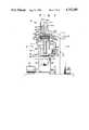
- FIG. 1is a perspective view schematically showing a wafer bonding system which uses a bonding apparatus according to an embodiment of the present invention
- FIG. 2is a partially broken side view showing a bonding apparatus according to the embodiment of the present invention with wafers mounted and chucked;
- FIG. 3is a partially broken side view showing the apparatus with wafers opposing each other and the center of a mirror surface of an upper wafer projecting;
- FIGS. 4A to 4Care sectional views showing a part of the apparatus in each step which illustrates a method of bonding wafers.
- FIG. 5is a sectional view showing a part of a modified mechanism.
- FIG. 1shows a wafer bonding system which uses a wafer bonding apparatus of the present invention comprising first and second supports 2 and 4.
- Rectangular enclosure 8 with an open front and a transparent top and clean unit 10 positioned therebehindare provided on pedestal 6.
- a filter(not shown) which cleans air supplied horizontally from a blower of the clean unit to the enclosure is provided between unit 10 and enclosure 8. With this mechanism, the interior of enclosure 8 is kept clean.
- first and second supports 2 and 4are installed adjacent and opposite each other and panel 12 and TV monitor 14 are spaced apart from supports 2 and 4.
- Monitor camera 16is positioned at a distance of, e.g., 500 mm from and above the top surface of enclosure 8. Operations of supports 2 and 4 are monitored by camera 16 and displayed on TV monitor 14. Operations of supports 2 and 4 can be controlled by observing TV monitor 14 and operating panel 12.
- first and second supports 2 and 4have first and second chuck tables 20a and 20b, respectively.
- Tables 20a and 20bcomprise disk-like first and second elastic bases 24a and 24b.
- Base 24a and 24bhave flat surfaces on which semiconductor wafers 22a, 22b are mounted with their mirror surfaces facing up.
- Bases 24a and 24bmay be made of an elastic material such as rubber, or a material which is not elastic itself but imparts elasticity upon being formed into a thin member.
- Bases 24a and 24bhave a plurality of through holes 26a and 26b, respectively. These holes are preferably formed near the periphery of the base such that the center of the base is conveniently projected.
- Tables 20a and 20bhave support members 30a and 30b which support bases 24a and 24b on their upper surfaces, respectively.
- Members 30a and 30bare cylindrical with their upper portions enlarged horizontally.
- Cavities 28a and 28b whose upper surfaces are closed by elastic bases 24a and 24bare formed in the upper portions of support members 30a and 30b.
- Paths 34a and 32bare respectively formed in support members 30a and 30b so that their upper ends communicate with cavities 28a and 28b and their lower ends are open at the lower surfaces of support members 30a and 30b.
- Projecting member 34which faces the other surface of base 24b and projects at the center thereof is vertically movably housed in cavity 28b of table 20b of support 4. More specifically, an upper surface of projecting member 34 is conical. Columnar sliding portion 37 projects from the lower surface of projecting portion 34 and is slidable with respect to the inner upper wall of path 32b of support member 30b. Path 36 is formed in projecting member 34 so that its lower end is open at the lower surface of sliding portion 37 and its upper end at the conical surface. Path 36 normally communicates cavity 28b with path 32b. Lower ends of paths 32a and 32b of support members 30a and 30b are respectively communicated with vacuum pumps 33a and 33b for evacuating paths 32a and 32b. Wafers 22a and 22b respectively mounted on bases 24a and 24b are drawn upon operation of vacuum pumps through paths 32a and 32b, cavities 28a and 28b, and holes 26a and 26b, and are chucked to surfaces of bases 24a and 24b.
- Support member 30bis slidably fitted in a vertical through hole in bracket 42 mounted on one end of rotating arm 40. In the state shown in FIG. 2, support member 30b is held such that its lower surface is in contact with the upper surface of bracket 42.
- First fixing member 54ais mounted on a lower portion of support portion 30b projecting from the lower end of bracket 42, and fixes at its one end first terminal 52a constituting a contact sensor for wafers.
- Second terminal 52bcooperates with terminal 52a to constitute the sensor.
- Terminal 52bis coaxial and at a predetermined distance from terminal 52a, and is fixed by second fixing member 54b projecting horizontally on the lower portion of bracket 42 of arm 40.
- the contact sensorgenerates an electrical signal when its terminals are not in contact with each other.
- the contact sensoris electrically connected to a motor so as to close a drive circuit of a Z pulse motor which is described later, and to a drive circuit of a vacuum pump for evacuating a pedestal so as to stop the operation of the pump by an electrical signal.
- Coil spring 55is arranged between fixing members 54a and 54b so as to bias first fixing member 54a downwardly.
- Arm 40is mounted through shaft 46 on arm support column 44 whose lower portion is fixed to pedestal 6 so as to pivot about the shaft in a vertical plane.
- Shaft 46is rotated by motor 48 via a known transmission mechanism in column 44.
- First support 2comprises block 3 which supports table 20a to be rotatable and vertically movable, and X, Y, Z, and ⁇ pulse motors 60, 62, 64, and 66.
- Motors 60 and 62can move X-Y stage 68 horizontally, i.e., in X and Y directions by desired amounts.
- Block 3is mounted on X-Y stage 68 to move therewith.
- Z and ⁇ moving mechanismis installed in block 3.
- Bolt 76is connected through joint member 74 to rotating shaft 72 of motor 64 which is fixed to block 3.
- Bolt 76is screwed into a female threaded through hole formed in lift plate 78.
- the lift plateis connected to support member 30a to be free from rotation of support member 30a and interlocked with vertical movement thereof.
- a connecting mechanismcomprising a recess which is formed at an outer periphery of support member 30b and engageable with a projection provided on plate 78 can be adopted.
- First gear 82is coaxially mounted on rotating shaft 80 of motor 66 which is fixed to block 3.
- Gear 82is meshed with second gear 84 which is coaxially mounted on the lower portion of support member 30a.
- Gears 82 and 84are arranged such that gear 82 is meshed with gear 84 and is free from vertical movement thereof.
- Wafers 22a and 22b having mirror surface finished upper surfacesare respectively chucked on first and second elastic bases 22a and 22b by evacuating table 20a and 20b.
- motor 48is driven to pivot arm 40 counterclockwise through 180°.
- second support member 30bmoves downwardly against the biasing force of spring 55 by its own weight and is held where first terminal 52a is in contact with second terminal 52b.
- projecting member 34moves downwardly by its own weight and urges base 24b such that the center portion thereof projects downwardly. It will be obvious that vertical alignment of support member 30b and a projection action of the wafer can be achieved automatically by pivoting arm 40 through 180°.
- support member 30ais horizontally shifted and pivoted by driving and controlling X, Y, and ⁇ motors 60, 62, and 66 to match orientation flats of both wafers.
- Z motor 64is driven to move support member 30a upwardly to bring wafer 22a into contact with the central portion of wafer 22b, as shown in FIG. 4B.
- the second wafer or the second support memberis slightly shifted upwardly, terminals 52a and 52b are disconnected, and an electric signal is generated to stop motor 64 and the vacuum pumps.
- wafer 22bwhose central portion projects downwardly is released from suction by base 24b.
- a bonding region of wafers 22a and 22bextends from the central portion to the periphery to prevent air bubbles from being trapped in the interface.
- a projecting membermay be arranged so as to project lower wafers, or the central portions of two wafers may be projected.
- a means for moving the projecting membersis required.
- a semiconductor waferis projected and then moved to be brought into contact with another semiconductor wafer at their central portions.
- semiconductor wafersmay be brought into contact with each other by projecting the central portion(s) of the wafer(s).
- the projecting member and the support memberare provided independently of each other. However, they may be formed as an integral structure, as will be described with reference to FIG. 5.
- Cylindrical support member 100is formed such that it has lower portion 100a, which extends through bracket 42 and is slidable in the axial direction thereof, and upper portion 100b, which is projected from the upper surface of bracket 42 and has a diameter larger than that of lower portion 100a.
- the upper surface of upper portion 100bis formed to be conical, thus forming a projecting member.
- Straight path 36is provided in upper portion 100b such that it is open at the circumference of upper portion 100b. This path communicates with path 32b provided in lower portion 100a.
- Cylindrical support base 24bmade of an elastic material such as rubber, is attached to the upper portion of support member 100 such that the interior of support base 24b defines a space sealed by upper portion 100b.
- Support base 24bis provided with through holes 26a at a position shifted from the center thereof.
Landscapes
- Engineering & Computer Science (AREA)
- Physics & Mathematics (AREA)
- Condensed Matter Physics & Semiconductors (AREA)
- General Physics & Mathematics (AREA)
- Manufacturing & Machinery (AREA)
- Computer Hardware Design (AREA)
- Microelectronics & Electronic Packaging (AREA)
- Power Engineering (AREA)
- Container, Conveyance, Adherence, Positioning, Of Wafer (AREA)
Abstract
Description
The present invention relates to a method for handling mirror surface finished semiconductor wafers and an apparatus therefor.
In a typical technique used in the manufacture of semiconductor devices, a semiconductor layer of a specific conductivity type is formed on a semiconductor substrate by a CVD method and a functional element is formed in this region. In this CVD method, it is necessary to prevent an impurity from diffusing or mixing in from the substrate into the semiconductor layer.
Recently, a demand for an element with a high dielectric withstand voltage is high. Dielectric withstand voltage can be improved by thickening the semiconductor layer. However, it takes extremely long time to do this by the CVD method, and it is more difficult to prevent a diffusing of impurity.
In the invention described in Japanese patent publication No. 49-26455, semiconductor wafers are bonded such that semiconductor layers oppose each other, so as to prevent impurity mixing and to reduce manufacturing time as compared with the case wherein a semiconductor layer is formed using the CVD method. The method is performed as follows. Mirror surface finished semiconductor wafers are placed to oppose each other in an atmosphere of a gas mixture consisting of oxygen and nitrogen, and phosphorus is diffused into each mirror surface at a temperature of 1,200° C. for 30 minutes using phosphorus oxychloride as an impurity. The wafers are then heated at a temperature of 1,150° C. for an hour. After placing the wafers in a vacuum, the wafers are bonded at a pressure of 150 kg/cm2 and a temperature of 1,300° C.
However, when a bonding temperature is higher than that during diffusion as described above, the diffusion impurity is redistributed during bonding to change a surface concentration of an impurity layer. In addition, wafer alignment in a vacuum is difficult to perform and results in high cost.
In order to solve the above problem, a method of bonding wafers in air at room temperature is disclosed by the present inventor in "Nikkei Electronics", Jan. 27, 1986, p. 108 to 110. In this method, after the mirror surfaces of wafers are washed with water and excess water is removed, the wafers are bonded together in a clean atmosphere utilizing residual water on the mirror surfaces. According to this method, impurity redistribution is prevented and wafer alignment is easy.
However, in this method, air bubbles are left between wafers to form voids in their interfaces.
It is an object of the present invention to provide a method of handling wafers without forming voids even when wafers are bonded in air at room temperature, and a mechanism therefor.
FIG. 1 is a perspective view schematically showing a wafer bonding system which uses a bonding apparatus according to an embodiment of the present invention;
FIG. 2 is a partially broken side view showing a bonding apparatus according to the embodiment of the present invention with wafers mounted and chucked;
FIG. 3 is a partially broken side view showing the apparatus with wafers opposing each other and the center of a mirror surface of an upper wafer projecting;
FIGS. 4A to 4C are sectional views showing a part of the apparatus in each step which illustrates a method of bonding wafers; and
FIG. 5 is a sectional view showing a part of a modified mechanism.
An embodiment of the present invention will now be described with reference to the accompanying drawings.
FIG. 1 shows a wafer bonding system which uses a wafer bonding apparatus of the present invention comprising first andsecond supports Rectangular enclosure 8 with an open front and a transparent top andclean unit 10 positioned therebehind are provided on pedestal 6. A filter (not shown) which cleans air supplied horizontally from a blower of the clean unit to the enclosure is provided betweenunit 10 andenclosure 8. With this mechanism, the interior ofenclosure 8 is kept clean. Inenclosure 8 on pedestal 6, first andsecond supports panel 12 andTV monitor 14 are spaced apart fromsupports Monitor camera 16 is positioned at a distance of, e.g., 500 mm from and above the top surface ofenclosure 8. Operations ofsupports camera 16 and displayed onTV monitor 14. Operations ofsupports TV monitor 14 andoperating panel 12.
As shown in FIG. 2, first andsecond supports elastic bases Bases Bases holes members bases Members Cavities elastic bases support members Paths 34a and 32b are respectively formed insupport members cavities support members
Projectingmember 34 which faces the other surface ofbase 24b and projects at the center thereof is vertically movably housed incavity 28b of table 20b ofsupport 4. More specifically, an upper surface of projectingmember 34 is conical.Columnar sliding portion 37 projects from the lower surface of projectingportion 34 and is slidable with respect to the inner upper wall ofpath 32b ofsupport member 30b.Path 36 is formed in projectingmember 34 so that its lower end is open at the lower surface of slidingportion 37 and its upper end at the conical surface.Path 36 normally communicatescavity 28b withpath 32b. Lower ends ofpaths support members vacuum pumps 33a and 33b for evacuatingpaths Wafers 22a and 22b respectively mounted onbases paths cavities holes bases
A method of bonding semiconductor wafers using a bonding apparatus having the above construction will now be described with reference to FIGS. 3 and 4A to 4C.
In the above embodiment, the projecting member and the support member are provided independently of each other. However, they may be formed as an integral structure, as will be described with reference to FIG. 5.
With the support member having the above construction, if the air in thesupport base 24b throughpaths support base 24b is pulled to supportmember 100 and deformed into a conical shape that conforms with the shape of the upper portion ofsupport member 100. At this time,wafer 22b is deformed together withelastic member 24b in such a manner that the peripheral portions ofwafer 22b are pulled toward the projecting member more greatly than the central portion. Accordingly, the central portion ofwafer 22b is projected, as in the embodiment described above.
Claims (13)
1. A method of handling semiconductor wafers comprising the steps of:
projecting a central portion of a mirror surface of at least one wafer of two semiconductor wafers having mirror surfaces;
opposing said two wafers to each other and bringing the central portions of the mirror surfaces of the two wafers into contact with each other; and
enlarging a contact region from the central portions to peripheries of the mirror surfaces of the wafers.
2. A method according to claim 1, wherein said projecting step comprises the step of flattening the mirror surface of one wafer and projecting the central portion of the mirror surface of the other wafer toward said one wafer.
3. A method according to claim 2, wherein said projecting step comprises the step of conically projecting the mirror surface of the other wafer.
4. A method according to claim 3, wherein said method comprises the step of opposing said wafers each other and aligning them before said projecting step.
5. An apparatus for handling semiconductor wafers comprising:
first and second tables, having respective first and second elastic bases, said first and second elastic bases each having first and second surfaces, each of said first surfaces being adapted to receive a semiconductor wafer having a mirror surface facing up and the other surface of the semiconductor wafer in contact with the first surface of the elastic base, and a plurality of through holes extending from the first to the second surfaces of said elastic base;
a suction mechanism for reducing pressure in said through holes to chuck the semiconductor wafers to said bases;
a projecting mechanism, provided to face the other surface of at least said second base, for urging against said elastic base to elastically deform said base, thereby projecting a central portion of said elastic base to deform the mirror surface of the semiconductor wafer into a substantially convex shape;
first and second support mechanisms for supporting said first and second tables and said projecting mechanism; and
drive means for moving said first and second support mechanisms relative to each other and pressing the mirror surfaces of the semiconductor wafers into contact with each other.
6. An apparatus according to claim 5, wherein said first and second elastic bases are supported at one ends of the first and second support members, the support members having shafts and paths which communicate with said through holes of said bases, and said suction mechanism evacuates said paths of said first and second support members to reduce pressure in said through holes.
7. An apparatus according to claim 6, wherein said first support mechanism has a block which supports said first table pivotally about its axis and movably along the axis.
8. An apparatus according to claim 7, wherein said drive means comprises a rotating mechanism for rotating said first table with respect to the block and a moving mechanism for axially moving said first table with respect to said block.
9. An apparatus according to claim 8, wherein said apparatus comprises an X-Y table having said block thereon.
10. An apparatus according to claim 6, wherein said second support mechanism comprises an arm for axially and movably supporting said second table and a support column for pivotally supporting said arm, and said drive means comprises an arm pivoting mechanism for pivoting said arm to allow the semiconductor wafer on said second elastic base to face the semiconductor wafer on said first elastic base.
11. An apparatus according to claim 10, wherein said projecting mechanism comprises a projecting member provided axially and movably in the path of said second table and having at a center of one end surface thereof a projection capable of being brought into contact with the other surface of said second elastic base.
12. An apparatus according to claim 11, wherein one end surface of said projecting member is conical.
13. An apparatus according to claim 5, which comprises a sensor which senses the contact between the central portions of said semiconductor wafers and thereupon releases evacuation in said through holes of the second elastic base.
Applications Claiming Priority (2)
| Application Number | Priority Date | Filing Date | Title |
|---|---|---|---|
| JP60-25173 | 1985-02-14 | ||
| JP2517385AJPS61185916A (en) | 1985-02-14 | 1985-02-14 | Semiconductor wafer bonding method and bonding mechanism |
Publications (1)
| Publication Number | Publication Date |
|---|---|
| US4752180Atrue US4752180A (en) | 1988-06-21 |
Family
ID=12158612
Family Applications (1)
| Application Number | Title | Priority Date | Filing Date |
|---|---|---|---|
| US06/895,814Expired - LifetimeUS4752180A (en) | 1985-02-14 | 1986-08-12 | Method and apparatus for handling semiconductor wafers |
Country Status (1)
| Country | Link |
|---|---|
| US (1) | US4752180A (en) |
Cited By (34)
| Publication number | Priority date | Publication date | Assignee | Title |
|---|---|---|---|---|
| US4908092A (en)* | 1987-01-20 | 1990-03-13 | Ikegami Tsushinki Co., Ltd. | Apparatus for mounting chip device on printed circuit board |
| EP0415340A1 (en)* | 1989-08-28 | 1991-03-06 | Kabushiki Kaisha Toshiba | Method and apparatus for bonding semiconductor substrates |
| US5273553A (en)* | 1989-08-28 | 1993-12-28 | Kabushiki Kaisha Toshiba | Apparatus for bonding semiconductor substrates |
| US5300175A (en)* | 1993-01-04 | 1994-04-05 | Motorola, Inc. | Method for mounting a wafer to a submount |
| US5336029A (en)* | 1990-11-30 | 1994-08-09 | Kabushiki Kaisha Shibaura Seisakusho Sony Corp | Loading apparatus having a suction-hold mechanism |
| FR2703187A1 (en)* | 1993-03-10 | 1994-09-30 | Mitsubishi Electric Corp | Apparatus for separating a tablet from a support plate |
| US5843832A (en)* | 1995-03-01 | 1998-12-01 | Virginia Semiconductor, Inc. | Method of formation of thin bonded ultra-thin wafers |
| USRE36890E (en)* | 1990-07-31 | 2000-10-03 | Motorola, Inc. | Gradient chuck method for wafer bonding employing a convex pressure |
| US20030013273A1 (en)* | 2001-07-13 | 2003-01-16 | Mitsubishi Denki Kabushiki Kaisha | Method of manufacturing SOI wafer |
| US20030034110A1 (en)* | 2001-08-16 | 2003-02-20 | Wacker Siltronic Gesellschaft Fur Halbleitermaterialien Ag | Method and device for producing an adhesive-bonded connection between a semiconductor wafer and a carrier plate |
| US6578893B2 (en) | 2000-10-02 | 2003-06-17 | Ajs Automation, Inc. | Apparatus and methods for handling semiconductor wafers |
| US20030115747A1 (en)* | 2001-12-21 | 2003-06-26 | Esec Trading Sa, A Swiss Corporation | Pick-up tool for mounting semiconductor chips |
| US20050221582A1 (en)* | 2003-12-31 | 2005-10-06 | Chippac, Inc. | Bonding tool for mounting semiconductor chips |
| US20060141742A1 (en)* | 2002-12-09 | 2006-06-29 | Franck Fournel | Method of producing a complex structure by assembling stressed structures |
| WO2006005327A3 (en)* | 2004-07-15 | 2006-08-10 | Pac Tech Gmbh | Method and device for the alternate contacting of two wafers |
| US20070044294A1 (en)* | 1997-06-12 | 2007-03-01 | Dai Nippon Printing Co., Ltd. | Apparatus for manufacturing a wiring board and method for manufacturin a wiring board |
| US20070094886A1 (en)* | 2005-10-04 | 2007-05-03 | Applied Materials, Inc. | Methods and apparatus for drying a substrate |
| US20070194438A1 (en)* | 2004-03-26 | 2007-08-23 | Kosuke Takasaki | Device And Method For Joining Substrates |
| US20070297878A1 (en)* | 2006-06-20 | 2007-12-27 | Nec Electronics Corporation | Substrate transfer apparatus featuring lower and upper pneumatic sucker arms, and substrate transfer method carried ou in such substrate transfer apparatus |
| US20080128081A1 (en)* | 2006-12-04 | 2008-06-05 | Stats Chippac, Inc. | Pick-up heads and systems for die bonding and related applications |
| US20080279659A1 (en)* | 2007-05-07 | 2008-11-13 | Lintec Corporation | Transferring device and transferring method |
| US20080299245A1 (en)* | 2007-05-31 | 2008-12-04 | Sacmi Cooperativa Meccanici Imola Societa'cooperativa | Unit for picking up ceramic products or the like |
| US20090311818A1 (en)* | 2005-04-08 | 2009-12-17 | Shinichi Sueyoshi | Anodic bonding method and method of producing acceleration sensor |
| US20100097738A1 (en)* | 2008-10-20 | 2010-04-22 | Samsung Electro-Mechanics Co., Ltd. | Electrostatic chuck and substrate bonding device using the same |
| US20110035936A1 (en)* | 2009-08-11 | 2011-02-17 | Samsung Electronics Co., Ltd. | Semiconductor chip attaching apparatus and method |
| US20110142573A1 (en)* | 2009-12-10 | 2011-06-16 | Wendell Thomas Blonigan | Auto-sequencing multi-directional inline processing apparatus |
| EP2405465A1 (en)* | 2010-07-07 | 2012-01-11 | S.O.I. Tec Silicon on Insulator Technologies | Bonding method by molecular bonding with radial misalignment compensation |
| KR101236219B1 (en) | 2010-09-23 | 2013-02-22 | 소이텍 | Direct bonding method with reduction in overlay misalignment |
| US20130309046A1 (en)* | 2010-10-15 | 2013-11-21 | Ev Group Gmbh | Device and method for processing of wafers |
| WO2014191033A1 (en)* | 2013-05-29 | 2014-12-04 | Ev Group E. Thallner Gmbh | Device and method for bonding substrates |
| US9462921B2 (en) | 2011-05-24 | 2016-10-11 | Orbotech LT Solar, LLC. | Broken wafer recovery system |
| WO2018028801A1 (en)* | 2016-08-12 | 2018-02-15 | Ev Group E. Thallner Gmbh | Method and sample holder for the controlled bonding of substrates |
| TWI622114B (en)* | 2016-07-29 | 2018-04-21 | Debonding and leveling device and debonding method | |
| US10985302B2 (en)* | 2014-10-31 | 2021-04-20 | eLux, Inc. | Pick-and-remove system with deformable contact surface |
Citations (8)
| Publication number | Priority date | Publication date | Assignee | Title |
|---|---|---|---|---|
| JPS4926455A (en)* | 1972-07-11 | 1974-03-08 | ||
| US3887783A (en)* | 1972-11-09 | 1975-06-03 | Honeywell Bull Sa | Devices for welding of integrated-circuit wafers |
| US3921885A (en)* | 1973-06-28 | 1975-11-25 | Rca Corp | Method of bonding two bodies together |
| US4181249A (en)* | 1977-08-26 | 1980-01-01 | Hughes Aircraft Company | Eutectic die attachment method for integrated circuits |
| US4196837A (en)* | 1977-09-23 | 1980-04-08 | Siemens Aktiengesellschaft | Method of indirectly connecting two parts |
| US4226569A (en)* | 1977-04-20 | 1980-10-07 | Thomson-Csf | Wafer loading and positioning device |
| US4409278A (en)* | 1981-04-16 | 1983-10-11 | General Electric Company | Blister-free direct bonding of metals to ceramics and metals |
| US4529353A (en)* | 1983-01-27 | 1985-07-16 | At&T Bell Laboratories | Wafer handling apparatus and method |
- 1986
- 1986-08-12USUS06/895,814patent/US4752180A/ennot_activeExpired - Lifetime
Patent Citations (8)
| Publication number | Priority date | Publication date | Assignee | Title |
|---|---|---|---|---|
| JPS4926455A (en)* | 1972-07-11 | 1974-03-08 | ||
| US3887783A (en)* | 1972-11-09 | 1975-06-03 | Honeywell Bull Sa | Devices for welding of integrated-circuit wafers |
| US3921885A (en)* | 1973-06-28 | 1975-11-25 | Rca Corp | Method of bonding two bodies together |
| US4226569A (en)* | 1977-04-20 | 1980-10-07 | Thomson-Csf | Wafer loading and positioning device |
| US4181249A (en)* | 1977-08-26 | 1980-01-01 | Hughes Aircraft Company | Eutectic die attachment method for integrated circuits |
| US4196837A (en)* | 1977-09-23 | 1980-04-08 | Siemens Aktiengesellschaft | Method of indirectly connecting two parts |
| US4409278A (en)* | 1981-04-16 | 1983-10-11 | General Electric Company | Blister-free direct bonding of metals to ceramics and metals |
| US4529353A (en)* | 1983-01-27 | 1985-07-16 | At&T Bell Laboratories | Wafer handling apparatus and method |
Non-Patent Citations (2)
| Title |
|---|
| Yoshikawa, K., "Nikkei Electronics", Jan. 27, 1986, pp. 108-110. |
| Yoshikawa, K., Nikkei Electronics , Jan. 27, 1986, pp. 108 110.* |
Cited By (87)
| Publication number | Priority date | Publication date | Assignee | Title |
|---|---|---|---|---|
| US4908092A (en)* | 1987-01-20 | 1990-03-13 | Ikegami Tsushinki Co., Ltd. | Apparatus for mounting chip device on printed circuit board |
| EP0415340A1 (en)* | 1989-08-28 | 1991-03-06 | Kabushiki Kaisha Toshiba | Method and apparatus for bonding semiconductor substrates |
| US5129827A (en)* | 1989-08-28 | 1992-07-14 | Kabushiki Kaisha Toshiba | Method for bonding semiconductor substrates |
| US5273553A (en)* | 1989-08-28 | 1993-12-28 | Kabushiki Kaisha Toshiba | Apparatus for bonding semiconductor substrates |
| USRE36890E (en)* | 1990-07-31 | 2000-10-03 | Motorola, Inc. | Gradient chuck method for wafer bonding employing a convex pressure |
| US5336029A (en)* | 1990-11-30 | 1994-08-09 | Kabushiki Kaisha Shibaura Seisakusho Sony Corp | Loading apparatus having a suction-hold mechanism |
| US5300175A (en)* | 1993-01-04 | 1994-04-05 | Motorola, Inc. | Method for mounting a wafer to a submount |
| FR2703187A1 (en)* | 1993-03-10 | 1994-09-30 | Mitsubishi Electric Corp | Apparatus for separating a tablet from a support plate |
| US5447596A (en)* | 1993-03-10 | 1995-09-05 | Mitsubishi Denki Kabushiki Kaisha | Apparatus for producing semiconductor wafers |
| US5843832A (en)* | 1995-03-01 | 1998-12-01 | Virginia Semiconductor, Inc. | Method of formation of thin bonded ultra-thin wafers |
| US7526859B2 (en)* | 1997-06-12 | 2009-05-05 | Dai Nippon Printing Co., Ltd. | Apparatus for manufacturing a wiring board |
| US20070044294A1 (en)* | 1997-06-12 | 2007-03-01 | Dai Nippon Printing Co., Ltd. | Apparatus for manufacturing a wiring board and method for manufacturin a wiring board |
| US6578893B2 (en) | 2000-10-02 | 2003-06-17 | Ajs Automation, Inc. | Apparatus and methods for handling semiconductor wafers |
| US20030013273A1 (en)* | 2001-07-13 | 2003-01-16 | Mitsubishi Denki Kabushiki Kaisha | Method of manufacturing SOI wafer |
| US6844242B2 (en)* | 2001-07-13 | 2005-01-18 | Renesas Technology Corp. | Method of manufacturing SOI wafer |
| US20030034110A1 (en)* | 2001-08-16 | 2003-02-20 | Wacker Siltronic Gesellschaft Fur Halbleitermaterialien Ag | Method and device for producing an adhesive-bonded connection between a semiconductor wafer and a carrier plate |
| US20030115747A1 (en)* | 2001-12-21 | 2003-06-26 | Esec Trading Sa, A Swiss Corporation | Pick-up tool for mounting semiconductor chips |
| US20060141742A1 (en)* | 2002-12-09 | 2006-06-29 | Franck Fournel | Method of producing a complex structure by assembling stressed structures |
| US7550052B2 (en)* | 2002-12-09 | 2009-06-23 | Commissariat A L'energie Atomique | Method of producing a complex structure by assembling stressed structures |
| US20050221582A1 (en)* | 2003-12-31 | 2005-10-06 | Chippac, Inc. | Bonding tool for mounting semiconductor chips |
| US7958628B2 (en) | 2003-12-31 | 2011-06-14 | Stats Chippac, Ltd. | Bonding tool for mounting semiconductor chips |
| US20100083494A1 (en)* | 2003-12-31 | 2010-04-08 | Chippac, Inc. | Bonding Tool for Mounting Semiconductor Chips |
| US7650688B2 (en)* | 2003-12-31 | 2010-01-26 | Chippac, Inc. | Bonding tool for mounting semiconductor chips |
| US7678211B2 (en)* | 2004-03-26 | 2010-03-16 | Fujifilm Corporation | Device and method for joining substrates |
| US20070194438A1 (en)* | 2004-03-26 | 2007-08-23 | Kosuke Takasaki | Device And Method For Joining Substrates |
| US7988803B2 (en) | 2004-03-26 | 2011-08-02 | Fujifilm Corporation | Device and method for joining substrates |
| US20100108237A1 (en)* | 2004-03-26 | 2010-05-06 | Fuji Photo Film Co., Ltd. | Device and method for joining substrates |
| US7882997B2 (en) | 2004-07-15 | 2011-02-08 | Pac Tech-Packaging Technologies Gmbh | Method and device for mutual contacting of two wafers |
| US20080171404A1 (en)* | 2004-07-15 | 2008-07-17 | Pac Tech- Packagin Technologies Gmbh | Method and Device For Mutual Contacting of Two Wafers |
| WO2006005327A3 (en)* | 2004-07-15 | 2006-08-10 | Pac Tech Gmbh | Method and device for the alternate contacting of two wafers |
| US8785292B2 (en)* | 2005-04-08 | 2014-07-22 | Lapis Semiconductor Co., Ltd. | Anodic bonding method and method of producing acceleration sensor |
| US20090311818A1 (en)* | 2005-04-08 | 2009-12-17 | Shinichi Sueyoshi | Anodic bonding method and method of producing acceleration sensor |
| US8635784B2 (en)* | 2005-10-04 | 2014-01-28 | Applied Materials, Inc. | Methods and apparatus for drying a substrate |
| US20070094886A1 (en)* | 2005-10-04 | 2007-05-03 | Applied Materials, Inc. | Methods and apparatus for drying a substrate |
| US20070297878A1 (en)* | 2006-06-20 | 2007-12-27 | Nec Electronics Corporation | Substrate transfer apparatus featuring lower and upper pneumatic sucker arms, and substrate transfer method carried ou in such substrate transfer apparatus |
| US8037918B2 (en)* | 2006-12-04 | 2011-10-18 | Stats Chippac, Inc. | Pick-up heads and systems for die bonding and related applications |
| US20080128081A1 (en)* | 2006-12-04 | 2008-06-05 | Stats Chippac, Inc. | Pick-up heads and systems for die bonding and related applications |
| US7875144B2 (en)* | 2007-05-07 | 2011-01-25 | Lintec Corporation | Transferring device and transferring method |
| US20080279659A1 (en)* | 2007-05-07 | 2008-11-13 | Lintec Corporation | Transferring device and transferring method |
| US20080299245A1 (en)* | 2007-05-31 | 2008-12-04 | Sacmi Cooperativa Meccanici Imola Societa'cooperativa | Unit for picking up ceramic products or the like |
| US20100097738A1 (en)* | 2008-10-20 | 2010-04-22 | Samsung Electro-Mechanics Co., Ltd. | Electrostatic chuck and substrate bonding device using the same |
| US8307543B2 (en)* | 2009-08-11 | 2012-11-13 | Samsung Electronics Co., Ltd. | Semiconductor chip attaching apparatus |
| US20110035936A1 (en)* | 2009-08-11 | 2011-02-17 | Samsung Electronics Co., Ltd. | Semiconductor chip attaching apparatus and method |
| US20110142573A1 (en)* | 2009-12-10 | 2011-06-16 | Wendell Thomas Blonigan | Auto-sequencing multi-directional inline processing apparatus |
| US8672603B2 (en) | 2009-12-10 | 2014-03-18 | Orbotech LT Solar, LLC. | Auto-sequencing inline processing apparatus |
| US20110139372A1 (en)* | 2009-12-10 | 2011-06-16 | Wendell Thomas Blonigan | Showerhead assembly for vacuum processing apparatus |
| US9287152B2 (en) | 2009-12-10 | 2016-03-15 | Orbotech LT Solar, LLC. | Auto-sequencing multi-directional inline processing method |
| US20110142572A1 (en)* | 2009-12-10 | 2011-06-16 | Wendell Thomas Blonigan | Auto-sequencing inline processing apparatus |
| US8444364B2 (en)* | 2009-12-10 | 2013-05-21 | Orbotech LT Solar, LLC. | Auto-sequencing multi-directional inline processing apparatus |
| KR101217682B1 (en) | 2010-07-07 | 2012-12-31 | 소이텍 | Method for molecular adhesion bonding with compensation for radial misalignment |
| CN102315149A (en)* | 2010-07-07 | 2012-01-11 | S.O.I.Tec绝缘体上硅技术公司 | Molecule adhesive bond method with radially misalignment compensation |
| US9818614B2 (en) | 2010-07-07 | 2017-11-14 | Sony Semiconductor Solutions Corporation | Apparatus for molecular adhesion bonding with compensation for radial misalignment |
| US8475612B2 (en) | 2010-07-07 | 2013-07-02 | Soitec | Method for molecular adhesion bonding with compensation for radial misalignment |
| FR2962594A1 (en)* | 2010-07-07 | 2012-01-13 | Soitec Silicon On Insulator | MOLECULAR ADHESION BONDING METHOD WITH RADIAL DESALIGNMENT COMPENSATION |
| EP2405465A1 (en)* | 2010-07-07 | 2012-01-11 | S.O.I. Tec Silicon on Insulator Technologies | Bonding method by molecular bonding with radial misalignment compensation |
| US9123631B2 (en) | 2010-07-07 | 2015-09-01 | Soitec | Method for molecular adhesion bonding with compensation for radial misalignment |
| CN102315149B (en)* | 2010-07-07 | 2015-11-25 | S.O.I.Tec绝缘体上硅技术公司 | There is the molecular adhesion associated methods that radial misalignment compensates |
| KR101236219B1 (en) | 2010-09-23 | 2013-02-22 | 소이텍 | Direct bonding method with reduction in overlay misalignment |
| US9771223B2 (en)* | 2010-10-15 | 2017-09-26 | Ev Group Gmbh | Device and method for processing of wafers |
| US20130309046A1 (en)* | 2010-10-15 | 2013-11-21 | Ev Group Gmbh | Device and method for processing of wafers |
| US9751698B2 (en) | 2010-10-15 | 2017-09-05 | Ev Group Gmbh | Device and method for processing wafers |
| US9462921B2 (en) | 2011-05-24 | 2016-10-11 | Orbotech LT Solar, LLC. | Broken wafer recovery system |
| KR20190142440A (en)* | 2013-05-29 | 2019-12-26 | 에베 그룹 에. 탈너 게엠베하 | Device and method for bonding substrates |
| US11697281B2 (en) | 2013-05-29 | 2023-07-11 | Ev Group E. Thallner Gmbh | Device and method for bonding substrates |
| US11020951B2 (en) | 2013-05-29 | 2021-06-01 | Ev Group E. Thallner Gmbh | Device and method for bonding substrates |
| EP3404698A1 (en)* | 2013-05-29 | 2018-11-21 | EV Group E. Thallner GmbH | Method and device for bonding substrates |
| WO2014191033A1 (en)* | 2013-05-29 | 2014-12-04 | Ev Group E. Thallner Gmbh | Device and method for bonding substrates |
| CN109616408A (en)* | 2013-05-29 | 2019-04-12 | Ev 集团 E·索尔纳有限责任公司 | Apparatus and method for bonding substrates |
| US10279575B2 (en) | 2013-05-29 | 2019-05-07 | Ev Group E. Thallner Gmbh | Device and method for bonding substrates |
| KR102059706B1 (en) | 2013-05-29 | 2019-12-26 | 에베 그룹 에. 탈너 게엠베하 | Device and method for bonding substrates |
| KR20190142442A (en)* | 2013-05-29 | 2019-12-26 | 에베 그룹 에. 탈너 게엠베하 | Device and method for bonding substrates |
| US11059280B2 (en) | 2013-05-29 | 2021-07-13 | Ev Group E. Thallner Gmbh | Device and method for bonding substrates |
| KR20190142441A (en)* | 2013-05-29 | 2019-12-26 | 에베 그룹 에. 탈너 게엠베하 | Device and method for bonding substrates |
| CN109616408B (en)* | 2013-05-29 | 2023-07-25 | Ev 集团 E·索尔纳有限责任公司 | Apparatus and method for bonding substrates |
| KR102164855B1 (en) | 2013-05-29 | 2020-10-14 | 에베 그룹 에. 탈너 게엠베하 | Device and method for bonding substrates |
| KR102229805B1 (en) | 2013-05-29 | 2021-03-19 | 에베 그룹 에. 탈너 게엠베하 | Device and method for bonding substrates |
| US11020953B2 (en) | 2013-05-29 | 2021-06-01 | Ev Group E. Thallner Gmbh | Device and method for bonding substrates |
| TWI740127B (en)* | 2013-05-29 | 2021-09-21 | 奧地利商Ev集團E塔那有限公司 | Device and method for bonding of substrates |
| KR102258288B1 (en) | 2013-05-29 | 2021-05-31 | 에베 그룹 에. 탈너 게엠베하 | Device and method for bonding substrates |
| US11020952B2 (en) | 2013-05-29 | 2021-06-01 | Ev Group E. Thallner Gmbh | Device and method for bonding substrates |
| US11020950B2 (en) | 2013-05-29 | 2021-06-01 | Ev Group E. Thallner Gmbh | Device and method for bonding substrates |
| US10985302B2 (en)* | 2014-10-31 | 2021-04-20 | eLux, Inc. | Pick-and-remove system with deformable contact surface |
| TWI622114B (en)* | 2016-07-29 | 2018-04-21 | Debonding and leveling device and debonding method | |
| TWI649826B (en)* | 2016-08-12 | 2019-02-01 | 奧地利商Ev集團E塔那有限公司 | Method for controlling substrate bonding and holding device |
| US10991609B2 (en) | 2016-08-12 | 2021-04-27 | Ev Group E. Thallner Gmbh | Method and substrate holder for the controlled bonding of substrates |
| TWI681488B (en)* | 2016-08-12 | 2020-01-01 | 奧地利商Ev集團E塔那有限公司 | Method and holding device for the controlled bonding of substrates |
| WO2018028801A1 (en)* | 2016-08-12 | 2018-02-15 | Ev Group E. Thallner Gmbh | Method and sample holder for the controlled bonding of substrates |
Similar Documents
| Publication | Publication Date | Title |
|---|---|---|
| US4752180A (en) | Method and apparatus for handling semiconductor wafers | |
| EP0256150B1 (en) | Apparatus for bonding semiconductor wafers | |
| US4795299A (en) | Dial deposition and processing apparatus | |
| US5306380A (en) | Vacuum processing apparatus | |
| US7370681B2 (en) | Substrate bonding apparatus for liquid crystal display device | |
| US9837295B2 (en) | Apparatus and method for semiconductor wafer leveling, force balancing and contact sensing | |
| US5947675A (en) | Cassette transfer mechanism | |
| CN101960557A (en) | Room temperature bonding device | |
| JP2001356353A (en) | Board assembly equipment | |
| CN1654969A (en) | Electron Beam Testing System with Integrated Substrate Moving Module | |
| JP3386986B2 (en) | Plasma processing equipment | |
| JP3906753B2 (en) | Board assembly equipment | |
| US20150311101A1 (en) | Substrate transfer antechamber mechanism | |
| US6156125A (en) | Adhesion apparatus | |
| JP6471401B1 (en) | Semiconductor wafer test unit | |
| CN113053794A (en) | Pre-positioning bearing device and positioning bearing method | |
| KR100720423B1 (en) | Substrate bonding device for liquid crystal display device and flatness correction method using same | |
| JPH10135317A (en) | Substrate mounting table | |
| JP2004228313A (en) | Inspection equipment for semiconductor wafer | |
| US6384418B1 (en) | Sample transfer apparatus and sample stage | |
| WO2020261949A1 (en) | Wafer testing apparatus | |
| KR0108386Y1 (en) | Wafer bonding machine | |
| JPH044740B2 (en) | ||
| JP4470923B2 (en) | Board assembly equipment | |
| JP3817461B2 (en) | Assembling method of liquid crystal substrate |
Legal Events
| Date | Code | Title | Description |
|---|---|---|---|
| AS | Assignment | Owner name:KABUSHIKI KAISHA TOSHIBA, 72 HORIKAWA-CHO, SAIWAI- Free format text:ASSIGNMENT OF ASSIGNORS INTEREST.;ASSIGNOR:YOSHIKAWA, KIYOSHI;REEL/FRAME:004644/0055 Effective date:19860721 Owner name:KABUSHIKI KAISHA TOSHIBA, JAPAN Free format text:ASSIGNMENT OF ASSIGNORS INTEREST;ASSIGNOR:YOSHIKAWA, KIYOSHI;REEL/FRAME:004644/0055 Effective date:19860721 | |
| STCF | Information on status: patent grant | Free format text:PATENTED CASE | |
| CC | Certificate of correction | ||
| FEPP | Fee payment procedure | Free format text:PAYOR NUMBER ASSIGNED (ORIGINAL EVENT CODE: ASPN); ENTITY STATUS OF PATENT OWNER: LARGE ENTITY | |
| FPAY | Fee payment | Year of fee payment:4 | |
| FPAY | Fee payment | Year of fee payment:8 | |
| FPAY | Fee payment | Year of fee payment:12 |