US4751513A - Light controlled antennas - Google Patents
Light controlled antennasDownload PDFInfo
- Publication number
- US4751513A US4751513AUS06/858,771US85877186AUS4751513AUS 4751513 AUS4751513 AUS 4751513AUS 85877186 AUS85877186 AUS 85877186AUS 4751513 AUS4751513 AUS 4751513A
- Authority
- US
- United States
- Prior art keywords
- antenna
- diode
- light
- conductor
- photosensitive
- Prior art date
- Legal status (The legal status is an assumption and is not a legal conclusion. Google has not performed a legal analysis and makes no representation as to the accuracy of the status listed.)
- Expired - Fee Related
Links
- 239000000835fiberSubstances0.000claimsabstractdescription34
- 238000005286illuminationMethods0.000claimsabstractdescription6
- 239000004020conductorSubstances0.000claimsdescription123
- 239000004065semiconductorSubstances0.000claimsdescription34
- 230000008878couplingEffects0.000claimsdescription14
- 238000010168coupling processMethods0.000claimsdescription14
- 238000005859coupling reactionMethods0.000claimsdescription14
- 239000000463materialSubstances0.000claimsdescription11
- 230000004044responseEffects0.000claimsdescription11
- 230000005670electromagnetic radiationEffects0.000claimsdescription7
- IHQKEDIOMGYHEB-UHFFFAOYSA-Msodium dimethylarsinateChemical class[Na+].C[As](C)([O-])=OIHQKEDIOMGYHEB-UHFFFAOYSA-M0.000claimsdescription2
- 230000005855radiationEffects0.000description26
- 239000000758substrateSubstances0.000description26
- 230000005540biological transmissionEffects0.000description22
- 230000000694effectsEffects0.000description10
- 238000004519manufacturing processMethods0.000description8
- 239000012535impuritySubstances0.000description7
- 230000008859changeEffects0.000description6
- 238000010586diagramMethods0.000description5
- 238000001465metallisationMethods0.000description5
- 230000010287polarizationEffects0.000description5
- 229910052710siliconInorganic materials0.000description5
- 239000010703siliconSubstances0.000description5
- JBRZTFJDHDCESZ-UHFFFAOYSA-NAsGaChemical compound[As]#[Ga]JBRZTFJDHDCESZ-UHFFFAOYSA-N0.000description4
- XUIMIQQOPSSXEZ-UHFFFAOYSA-NSiliconChemical compound[Si]XUIMIQQOPSSXEZ-UHFFFAOYSA-N0.000description4
- 239000000853adhesiveSubstances0.000description4
- 230000001070adhesive effectEffects0.000description4
- 238000004891communicationMethods0.000description4
- 230000002441reversible effectEffects0.000description4
- 229910001218Gallium arsenideInorganic materials0.000description3
- 230000008901benefitEffects0.000description3
- 238000005530etchingMethods0.000description3
- WUPHOULIZUERAE-UHFFFAOYSA-N3-(oxolan-2-yl)propanoic acidChemical compoundOC(=O)CCC1CCCO1WUPHOULIZUERAE-UHFFFAOYSA-N0.000description2
- 239000004593EpoxySubstances0.000description2
- 238000010521absorption reactionMethods0.000description2
- 238000003491arrayMethods0.000description2
- 239000011324beadSubstances0.000description2
- 230000015572biosynthetic processEffects0.000description2
- 229910052980cadmium sulfideInorganic materials0.000description2
- 239000003990capacitorSubstances0.000description2
- 239000003365glass fiberSubstances0.000description2
- 238000000034methodMethods0.000description2
- 230000009467reductionEffects0.000description2
- 230000000717retained effectEffects0.000description2
- 238000004804windingMethods0.000description2
- ZOXJGFHDIHLPTG-UHFFFAOYSA-NBoronChemical compound[B]ZOXJGFHDIHLPTG-UHFFFAOYSA-N0.000description1
- MYMOFIZGZYHOMD-UHFFFAOYSA-NDioxygenChemical compoundO=OMYMOFIZGZYHOMD-UHFFFAOYSA-N0.000description1
- OAICVXFJPJFONN-UHFFFAOYSA-NPhosphorusChemical compound[P]OAICVXFJPJFONN-UHFFFAOYSA-N0.000description1
- 230000002411adverseEffects0.000description1
- 229910052790berylliumInorganic materials0.000description1
- ATBAMAFKBVZNFJ-UHFFFAOYSA-Nberyllium atomChemical compound[Be]ATBAMAFKBVZNFJ-UHFFFAOYSA-N0.000description1
- 230000000903blocking effectEffects0.000description1
- 229910052796boronInorganic materials0.000description1
- 230000001427coherent effectEffects0.000description1
- 230000003247decreasing effectEffects0.000description1
- 238000013461designMethods0.000description1
- 239000003989dielectric materialSubstances0.000description1
- 239000000428dustSubstances0.000description1
- 230000017525heat dissipationEffects0.000description1
- 230000006872improvementEffects0.000description1
- 239000012212insulatorSubstances0.000description1
- 229910052751metalInorganic materials0.000description1
- 239000002184metalSubstances0.000description1
- 230000005404monopoleEffects0.000description1
- 229910052698phosphorusInorganic materials0.000description1
- 239000011574phosphorusSubstances0.000description1
- 238000012545processingMethods0.000description1
- 230000001902propagating effectEffects0.000description1
- 230000001681protective effectEffects0.000description1
- 230000002829reductive effectEffects0.000description1
- 238000009877renderingMethods0.000description1
- 230000000284resting effectEffects0.000description1
- 230000035945sensitivityEffects0.000description1
- 238000000926separation methodMethods0.000description1
- 239000000779smokeSubstances0.000description1
- 230000000087stabilizing effectEffects0.000description1
- 238000012360testing methodMethods0.000description1
- 239000012815thermoplastic materialSubstances0.000description1
- XLYOFNOQVPJJNP-UHFFFAOYSA-NwaterChemical compoundOXLYOFNOQVPJJNP-UHFFFAOYSA-N0.000description1
Images


Classifications
- H—ELECTRICITY
- H01—ELECTRIC ELEMENTS
- H01Q—ANTENNAS, i.e. RADIO AERIALS
- H01Q1/00—Details of, or arrangements associated with, antennas
- H01Q1/12—Supports; Mounting means
- H01Q1/22—Supports; Mounting means by structural association with other equipment or articles
- H01Q1/24—Supports; Mounting means by structural association with other equipment or articles with receiving set
- H01Q1/247—Supports; Mounting means by structural association with other equipment or articles with receiving set with frequency mixer, e.g. for direct satellite reception or Doppler radar
- H—ELECTRICITY
- H01—ELECTRIC ELEMENTS
- H01Q—ANTENNAS, i.e. RADIO AERIALS
- H01Q3/00—Arrangements for changing or varying the orientation or the shape of the directional pattern of the waves radiated from an antenna or antenna system
- H01Q3/26—Arrangements for changing or varying the orientation or the shape of the directional pattern of the waves radiated from an antenna or antenna system varying the relative phase or relative amplitude of energisation between two or more active radiating elements; varying the distribution of energy across a radiating aperture
- H01Q3/2676—Optically controlled phased array
- H—ELECTRICITY
- H01—ELECTRIC ELEMENTS
- H01Q—ANTENNAS, i.e. RADIO AERIALS
- H01Q9/00—Electrically-short antennas having dimensions not more than twice the operating wavelength and consisting of conductive active radiating elements
- H01Q9/04—Resonant antennas
- H01Q9/0407—Substantially flat resonant element parallel to ground plane, e.g. patch antenna
- H01Q9/0442—Substantially flat resonant element parallel to ground plane, e.g. patch antenna with particular tuning means
- H—ELECTRICITY
- H01—ELECTRIC ELEMENTS
- H01Q—ANTENNAS, i.e. RADIO AERIALS
- H01Q9/00—Electrically-short antennas having dimensions not more than twice the operating wavelength and consisting of conductive active radiating elements
- H01Q9/04—Resonant antennas
- H01Q9/06—Details
- H01Q9/14—Length of element or elements adjustable
- H01Q9/145—Length of element or elements adjustable by varying the electrical length
Definitions
- This inventionrelates to antennas including photosensitive materials associated with the radiating for controlling electromagnetic radiation or other antenna characteristics in response to light.
- Modern electromagnetic communication and remote sensing systemsare using increasingly higher frequencies. High frequencies more readily accommodate the large bandwidths required by modern high data rate communications and by such sensing arrangements as chirp radar. Also, at higher frequencies the physical size of an antenna required to produce a given amount of gain is smaller than at lower frequencies. Some high frequencies are particularly advantageous or disadvantageous because of the physical transmission properties of the atmosphere at the particular frequency. For example, communications are disadvantageous at 23 gigahertz (GHz) because of the high path attenuation attributable to atmospheric water vapor, and at 55 GHz because of oxygen molecule absorption. On the other hand, frequencies near 40 GHz are particularly advantageous for communication and radar purposes in regions subject to smoke and dust because of the relatively low attenuation at those frequencies.
- GHzgigahertz
- each antenna element in the arrayWhen a high gain antenna array is required, it is advantageous for each antenna element in the array to have physically small dimensions in the arraying direction. For example, if it is desired to have a rectangular planar array of radiating elements for radiating in a direction normal or orthogonal to the plane of the array, it is desirable that the physical dimensions of each antenna element in the plane of the array be small so that they may be closely stacked. For those situations in which an antenna array uses a large number of radiating elements, it is also desirable that the radiating elements be substantially identical to each other so that the radiation patterns attributable to each radiating element are identical.
- RFradio frequency
- Antennas in the form of a rectangular conductive patch separated by a layer of dielectric material from a ground planeare known to provide certain advantages for millimeter wave operation, such as reasonable impedance match.
- Such antennasalso have a relatively broad beamwidth which is suitable for use in antenna arrays in which the beam scans a large angle.
- such antennasmay be readily fabricated by photographic techniques and arrayed together with strip transmission lines formed on the dielectric substrate.
- An antennaincludes a dielectric plate having first and second broad sides.
- a first flat conductive regionis attached to the first broad side and a second flat conductive region is also attached to the first broad side and separated from the first flat conductive region by a nonconductive gap.
- Another flat conductive surface attached to the second broad side of the dielectric platedefines a ground plane. The ground plane coacts with the first flat conductive region for, when energized, producing electromagnetic radiation with particular characteristics.
- a photosensitive semiconductor including first and second electrodeshas a first electrode coupled to the first flat conductive region and a second electrode coupled to the second flat conductive region for, when conductive, coupling the first and second flat conductive regions together for producing electromagnetic radiation when the coupled first and second flat conductive regions are energized at a frequency.
- a light generatoris coupled to the photosensitive semiconductor for biasing or controllably changing the electrical characteristics of the photosensitive semiconductor for controllably coupling the first and second flat conductive regions together for tuning the antenna for radiation at a frequency different then in the absence of light bias.
- the photosensitive semiconductoris a PIN diode.
- FIG. 1ais a perspective view, partially cut away, of a patch antenna as in the prior art, together with its tuning diodes, and FIG. 1b is a cross-sectional view of the prior art arrangement of FIG. 1a;
- FIG. 2ais a perspective view of an antenna according to the invention
- FIG. 2bis a cross section of the antenna of FIG. 2a in a direction 2B--2B
- FIG. 2cis a cross-sectional view of discrete PIN diode 230 illustrated in FIGS. 2a and 2b;
- FIG. 3is a diagram, partially in pictorial and partially in schematic form, illustrating the connections to the antenna illustrated in FIG. 2a for radiating energy therefrom;
- FIG. 4is a diagram, partially in pictorial and partially in schematic form, illustrating the connections of the antenna of FIG. 2a for use in receiving signals;
- FIGS. 5a and 5bare plots of return loss versus frequency of an antenna similar to that illustrated in FIG. 2a without either electrical bias or incident light, with electrical forward bias and with both electrical and light bias of its diode;
- FIGS. 6a and 6bare radiation patterns of an antenna similar to that illustrated in FIG. 2a without bias, with electrical forward bias and with both electrical and light bias of the diode;
- FIG. 7is a diagram of the space around an antenna being tested as an aid in understanding the conditions under which the radiation patterns of FIGS. 6a and 6b were made;
- FIG. 8ais a perspective view of another antenna embodying the invention and using fiber optic cables;
- FIG. 8bis a cross-sectional view of a portion of the antenna of FIG. 8a taken in the direction 8B--8B illustrating the feed connection;
- FIG. 8cis a cross-sectional view of a diode of the antenna of FIG. 8a illustrating the connection of a fiber optic cable to the diode;
- FIG. 8dillustrates in block diagram from a control arrangement including a control logic circuit for control of the antenna of FIG. 8a;
- FIG. 8eis a simplified schematic diagram of the control logic circuit of FIG. 8c;
- FIG. 8fis a plot illustrating the current distribution along the length of the antenna of FIG. 8e under a particular operating condition
- FIG. 9ais an exploded view of an antenna embodying the principles of the invention
- FIG. 9bis a cross section of portion of a structure of FIG. 9a illustrating internal details
- FIG. 9cis a cutaway perspective view of a portion of a packaged PIN diode which may be used in the arrangement of FIG. 9b;
- FIG. 10ais a perspective view of an array of antennas embodying the invention
- FIG. 10bis a cross section of the structure of FIG. 10a taken along the lines 10B--10B;
- FIGS. 11a and 11bare perspective and cross-sectional views, respectively, of another antenna embodying the invention.
- FIG. 12ais an exploded perspective view of another antenna embodying the invention
- FIG. 12bis a cross section of the structure of FIG. 12a in its assembled form, taken along the lines 12B--12B;
- FIG. 13is a cross section of an antenna similar to that of FIG. 12a illustrating an alternative method for illuminating the diodes by means of fiber optic cables;
- FIG. 14is a plan view of a semiconductor substrate illustrating a portion of an equiangular spiral antenna embodying the invention.
- FIGS. 15a-15fillustrate steps in the fabrication of a vertical PIN diode similar to that of FIG. 2c.
- FIG. 16illustrates a step in addition to those illustrated in FIGS. 15a-15f which may be used in the fabrication of the PIN diode of FIGS. 8c and 9c.
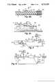
- FIG. 1aillustrates a prior art patch antenna, generally as described in U.S. Pat. No. 4,529,987 issued July 16, 1985, to Bhartia et al., cut away to illustrate some of the connections which must be made in such an arrangement.
- an antenna designated generally as 8in which the radiating element is a rectangular patch 10 of conductive material has path 10 separated froma conductive ground plane 11 by a thin dielectric layer 12.
- the bandwidth of the antennais increased by the provision of a pair of varactor diodes, one of which is illustrated as 15, connected between the edges of patch 10 and ground plane 11.
- FIG. 1bis a cross section of the arrangement of FIG. 1a looking in the direction of 1B--1B.
- the axial leads 20, 22 of diode 15extend through hole 18 and are bent to make contact with conductive patch 10 and with conductive ground plane 11, respectively.
- the leadsmay be soldered or welded to patch 10 and to ground plane 11 as required to maintain good electrical contact.
- An array of antennas similar to that of FIGS. 1a and 1bmay be expensive to manufacture.
- a plurality of conductive patchessuch as patch 10 are arrayed to form a multiple-antenna radiator, it is desirable that all the antennas have the same radiating characteristics and the same impedance characteristics.
- the radiating and impedance characteristics of the patch antennadepend upon the net reactances of the tuning diodes, such as diode 15. The net reactance depends upon the location and orientation of the diode within the hole which it occupies, the diameters of the leads 20 and 22, and upon the exact location on patch 10 at which leads 20 and 22 are attached.
- the net reactance of the tuning diodes of each antennaalso depends upon the reactance of each diode of the array under a given bias condition.
- An equal electrical biasmay be applied simultaneously to all diodes of the system by application of direct electrical bias over the common feed path (not illustrated in FIGS. 1a and 1b).
- the diodesmay exhibit different values of capacitance and/or resistance. Even if the diodes are matched, their reactances under a particular bias condition may differ slightly from one unit to another.
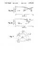
- FIG. 2ais a perspective view of an antenna 208 embodying the invention
- FIG. 2bis a cross section of a portion thereof taken along lines 2B--2B. Elements of FIGS. 2a and 2b corresponding to those of FIG. 1a are designated by the same reference numeral.
- a dielectric plate 12has affixed to its bottom a conductive ground plane 11. On the upper surface of plate 12 there are two separate structures and an interconnecting structure.
- the first structureincludes a flat conductive portion 10 which is essentially a patch radiator similar to that illustrated in FIG.
- the first structurealso includes an elongated third conductor 214 which coacts with ground plane 11 to act as a transmission line (not separately designated).
- Conductor 214extends from patch 10 along the upper surface of dielectric plate 12.
- a second structure associated with the upper surface of plate 12includes a further elongated conductor 216 which coacts with ground plane 11 to form a transmission line.
- Conductor 216is aligned with conductor 214 and is separated from conductor 214 by a gap 215.
- the end of conductor 216 remote from gap 215intersects the center of a further elongated conductor 218, the long dimension of which is oriented transverse to the long dimension of conductor 216.
- the ends of conductor 218 remote from the intersection with conductor 216are short-circuited to ground plane 11 by solenoidal windings or chokes, one of which is illustrated as 225 in FIG. 2b, inserted into hole 220.
- solenoidal windings or chokesone of which is illustrated as 225 in FIG. 2b, inserted into hole 220.
- FIG. 2athe locations of the holes into which DC short-circuiting solenoidal conductors such as 225 are inserted are illustrated by circles.
- a discrete diode 230is mounted on the end of conductor 216 adjacent gap 215.
- Diode 230is in the general shape of a circular cylinder.
- Diode 230has an electrode associated with its lower surface connected to conductor 216 and another electrode associated with its upper surface connected by way of a bond or jumper wire 232 to conductor 214.
- a controllable light source illustrated as 240produces light symbolized by arrows 242 which illuminates diode 230 for altering its conduction characteristic (resistance and capacitance) for controlling the characteristics of antenna 208.
- FIG. 2cis a cross section of diode 230 of FIGS. 2a and 2b.
- Diode 230 as illustrated in FIG. 2cincludes a semiconductor substrate 231, which may be silicon (Si) or gallium arsenide (GaAs) or any other photosensitive material.
- a semiconductor substrate 231which may be silicon (Si) or gallium arsenide (GaAs) or any other photosensitive material.
- Vertically stacked layers 250, 252 and 254 of wafer or substrate 231are heavily doped with acceptor impurities (p+), intrinsic (i), and heavily doped with electron donor impurities (n+), respectively.
- Layer 254is bonded to a metallized electrode contact 211, which is in turn bonded to conductor 216.
- An annular moat 256cuts through layers 250 and 252, and partially cuts through layer 254, to separate a central mesa 258 from the edges of the diode.
- the structuredefines a PIN diode.
- the upper surface of p+layer 250 in the region of mesa 258has bonded thereto an annular conductor 260 defining a central window or aperture 262 through which light 242 can enter the active or junction region of the diode structure.
- Important steps in the manufacture of a diode such as diode 230are illustrated in FIGS. 15a-15f. Bonding conductor 232 is connected to conductor 260, thereby making contact between conductor 214 (FIG. 2a) and upper metallization 260 of PIN diode 230.
- Such PIN diodesare photosensitive, and change their electrical characteristics when illuminated, whether electrically biased or not.
- an antennasuch as antenna 208 will radiate efficiently at a frequency established by the size of the aperture (the dimensions of patch 10 plus conductor 214) when the bias is such as to make diode 230 appear to be an open circuit or nonconductive.
- diode 230is biased so as to become partially or completely conductive, conductor 216 is excited by signal applied to patch 10 and conductor 214, and the size of the radiating aperture increases. Transmission-line like conductors 214 and 216 may actually radiate or merely change the characteristics of radiator 10. In any case, bias of diode 230 to render it conductive lowers the frequency of efficient antenna radiation.
- FIG. 3illustrates, partially in pictorial and partially in schematic form, the electrical connections required to radiate signal from a tuned antenna according to the invention and to apply electrical bias to the photosensitive portion of the antenna. Elements of FIG. 3 corresponding to elements of FIG. 2a and FIG. 2b are designated by the same reference number.
- a source 310produces microwave or millimeter wave alternating (AC) signals which are applied by way of transmission line conductor 212 to radiating patch 210 for producing electromagnetic radiation.
- the reactances associated with diode 230affect the radiation. Both the antenna radiation pattern and the radiating efficiency at a particular frequency may be controlled by control of the bias of diode 230.
- Light source 340illuminates diode 230 with light illustrated by arrow symbol 242.
- the lightchanges the AC conduction characteristics of the diode. This in turn changes the impedance of antenna 208 as seen at feed conductor 212.
- Light biasmay be used alone. It has been found that the effect of a given amount of illumination of diode 230 can be accentuated by application of an electrical bias.
- the biasincludes a direct voltage having a polarity which may be selected to forward or reverse bias the junction of diode 230.
- the bias voltageis generated by a source of direct voltage designated generally as 320 which includes series connected batteries 312 and 313 oonnected across a potentiometer 314 having a movable tap 316.
- the center point between batteries 312 and 313is connected to ground plane 11. Movement of tap 316 allows selection of any positive voltage up to the maximum voltage available from either battery 312 or any negative voltage up to the maximum voltage available from battery 313.
- Tap 316is connected to transmission line conductor 212 by means of a low pass filter illustrated as an inductor 318 which, as known, allows the direct bias voltage (or current) to be applied to transmission line conductor 212 (and therefore by way of patch antenna 10 to the anode of diode 230), but prevents or reduces leakage of millimeter wave signals from transmission line conductor 212 into source 320 of bias voltage.
- a low pass filterillustrated as an inductor 318 which, as known, allows the direct bias voltage (or current) to be applied to transmission line conductor 212 (and therefore by way of patch antenna 10 to the anode of diode 230), but prevents or reduces leakage of millimeter wave signals from transmission line conductor 212 into source 320 of bias voltage.
- Both direct voltage and direct currentare often abbreviated DC.
- Various types of low pass filtersare known in the art and further explanation is deemed unnecessary.
- the return path connection for bias voltage or currentincludes conductors 216, 218, choke solenoid
- Adjustment of the position of tab 316varies the bias voltage across diode 230, and therefore the current therethrough, which affects its conduction characteristic and adjusts the impedance and therefore the radiating characteristics of antenna 208.
- a forward bias voltageslightly less than the forward offset or junction voltage of the diode, little direct current flows. Slight increases in the bias voltages may cause disproportionate increases in conduction through diode 230, and at some point the current will be limited by the resistance of potentiometer 314.
- Reverse bias voltagescan also be applied to the diode by appropriate selection of the position of tap 316. Reverse bias voltages tend to make the diode impedance high and reduce its effect on the antenna, which may be desirable for some operating situations.
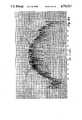
- FIG. 5aillustrates plots 510 and 512 of return loss of an antenna similar to antenna 208 as a function of the electrical bias condition of diode 230 in the absence of light.
- Diode 230in this case is a silicon PIN diode.
- Return lossis a measure of the amount of electrical signal reflected by a load (in this case, the antenna) back to the source of electrical signal, compared with the amount of signal applied from the source to the antenna. Such reflected signal cannot be utilized by the load, and may adversely effect operation of the signal source. It is desirable to have as large a return loss (greatest attenuation) as possible at the operating frequency so as to maximize the amount of signal utilized.
- utilizationcorresponds to signal radiation (except for I 2 R losses in the antenna).
- the return lossis a maximum of about 15 dB at about 10.28 GHz with zero electrical bias applied to diode 230, and with no illumination of the diode.
- Application of a forward bias current to diode 230 in the absence of lightcauses the diode to become significantly conductive, which in turn causes the frequency at which the return loss is maximized (maximum return loss, corresponding to maximum signal entering the antenna) to shift to about 10.20 GHz. This represents a downward shift in the tuning by about 80 megahertz (MHz)
- FIG. 5billustrates by a plot 514 the return loss occasioned by 0.5 volts of forward bias in the absence of light. Since diode 230 is a silicon diode, the 0.5 volts is less than the threshold voltage or forward junction potential of the diode, which is about 0.65 volts. The forward bias voltage is insufficient to overcome the junction potential of diode 230, and therefore the forward bias current flow is small. As illustrated, the return loss has a maximum value of about 19 dB at a frequency of approximately 10.17 GHz.
- Plot 516 of FIG. 5billustrates the result of illumination of diode 230 by white light having an intensity of one watt per square centimeter (W/centimeter 2 ). The application of light results in a downward shift of the radiating frequency of about 15 MHz, together with an improvement in the magnitude of the return loss by approximately 7 dB to about 26 dB.
- antennastransmission and reception of signals by an antenna are reciprocal, and that the antenna has the same gain, radiation pattern, and presents the same impedance to its terminals in both transmitting and receiving modes.
- antenna descriptionsare often couched in terms of "radiating" elements, “receiving” elements or the like, notwithstanding that the same elements having the same characteristics are involved, and the only difference is the direction of energy flow through what amounts to a transducer.
- FIG. 4illustrates, partially in pictorial and partially in schematic form, the electrical connections required to apply electrical bias to, and to receive signals from, a tuned antenna according to the invention. Elements of FIG. 4 corresponding to elements of FIG. 2a are designated by the same reference numeral.
- antenna 208receives millimeter wave signals which are coupled by way of transmission line conductor 212 and by a direct current blocking capacitor 410 to a receiver illustrated as a block 412 which may downconvert the received signal, demodulate and perform other known receiver functions.
- a source of direct voltage bias designated generally as 420includes a source of direct voltage illustrated as a variable battery 414 having its negative terminal electrically connected to ground plane 11 and its positive terminal connected by a low pass filter (illustrated as the series combination of an inducto 416 and a resistor 418) to transmission line conductor 212.
- a low pass filterillustrated as the series combination of an inducto 416 and a resistor 4128 to transmission line conductor 212.
- the bias voltage applied by way of transmission line conductor 212, patch 10 and conductor 214 to bias the anode of diode 230 relative to its cathodealso varies.
- the cathode of diode 230is connected by way of conductors 216 and 218, by solenoidal conductors 225 and 325 and by ground plane 11 to the negative terminal of battery 414.
- the impedance presented by antenna 208(patch antenna 10, diode 230 and its associated conductors) to the transmission line formed by conductor 212 in conjunction with ground plane 11, the gain and the receiving antenna pattern may be controlled by the bias applied to diode 230.
- forward bias voltage generated by battery 414having magnitudes less than the junction offset voltage of diode 230 results in relatively little current flow, and substantially the full bias voltage appears across diode 230.
- significant bias currentflows, limited principally by resistor 418 and the forward resistance of diode 230.
- FIGS. 6a and 6bwere made with the antenna of FIG. 2a operated in a receiving mode. However, due to the reciprocity of transmission and reception, the gain and radiation pattern of the antenna in the receiving mode are identical to those in the transmit mode.
- the antennais in effect mounted at the origin of a conventional coordinate system as illustrated in FIG. 7, with antenna ground plane 11 resting in the X-Y plane. With the antenna operated for reception, a linearly polarized transmitting antenna illustrated in FIG. 7 as 710 is rotated about its own axis so as to create a "spin-lin" condition in which the polarization of the transmitted signal is changed rapidly.
- the amplitude response of the antenna under test (antenna 208) operated in the receiving modeis plotted as a function of angle ⁇ to form plots such as those illustrated in FIGS. 6a and 6b.
- FIG. 6aillustrates as a plot 610 the radiation pattern made under a condition in which transmitting antenna 710 radiates at 10.285 GHz and in which diode 230 is not electrically biased.
- the change in amplitude attributable to the rapid change of polarization of the signal transmitted by antenna 710exceeds 10 dB, and antenna 208 may therefore be considered to be linearly polarized.
- the amplitude responseis substantially equal (within ⁇ 1 dB) for angles of ⁇ extending from -60° to +60°.
- Plot 612 of FIG. 6aillustrates the corresponding amplitude response of antenna 208 when diode 230 is forward biased with a finite current.
- the gainis reduced by approximately 1 dB (from a relative response of 9 dB to a relative response of 10 dB) as a result of forward bias, by comparison with zero bias of diode.
- Plots 614 and 616 of FIG. 6bwere made with antenna 710 (FIG. 7) transmitting at a frequency of 10.207 GHz. (a frequency 80 MHz below that at which the plots of FIG. 6a were made).
- Plot 614represents a zero biased diode
- plot 616represents a condition of forward current bias of diode 230. Consequently, while forward electrical bias of diode 230 caused a reduction in antenna gain compared with zero bias at 10.285 GHz, it caused an increase in gain of similar magnitude at 10.207 GHz.
- the bias of the diodeaffects the frequency of maximum return loss, without significant net effect on the radiation pattern or gain of the antenna.
- FIG. 8ais a perspective view
- FIG. 8bis a cross-sectional view of the feed portion of another antenna according to the invention.
- antenna 808includes a dielectric plate 812 having a conductive ground plane 811 attached to its bottom side.
- the broad top side of dielectric plate 812includes three axially aligned conductors 810, 814 and 816 separated by nonconductive gaps 815 and 817.
- a conductor 898extends from the bottom side of plate 812 through a hole illustrated in FIG. 8b as 896 to make contact with the end of conductor 810 which is remote from gap 815.
- Conductor 898is a portion of a feed transmission line corresponding to transmission line conductor 212 of FIG. 2a.
- a diode 830is mounted on the end of conductor 814 adjacent gap 815, and a further diode 880 is mounted on the end of conductor 816 adjacent gap 817.
- Each of diodes 830 and 880has one electrode connected to the conductor on which it sits, and further includes second, upper electrode.
- a bond wire 832connects the upper electrode of diode 830 to conductor 810 on the opposite side of adjacent gap 815.
- a similar bond wire 882connects the upper electrode of diode 880 across gap 817 to conductor 814.
- a fiber optic cable 892is connected to diode 830 and the other end is connected to a controllable light source illustrated as a block 890, and a fiber optic cable 894 has one end connected to diode 880 and the other connected to a further light source 888.
- any waveguide medium for propagating lightsuch as glass fibers, have a dielectric constant different from that of the surrounding region, which keeps light constrained therein along their length. In the case of glass fibers, the dielectric constant is higher than that of the surrounding medium
- Light sources 888 and 891are controlled by electrical conductors 897 and 891, respectively, from signal sources (not illustrated in FIGS. 8a or 8b).
- antenna 808When diodes 830 and 880 are nonconductive, antenna 808 includes as a radiating portion only conductor 810, which resonates at a frequency established by its dimension when energized from feed conductor 898.
- the radiating aperture of antenna 808When diode 830 is rendered conductive and diode 880 is nonconductive, the radiating aperture of antenna 808 includes conductor 810 and conductor 814, and the frequency at which radiation is most efficient is lower than when radiation takes place by conductor 810 alone.
- the radiating portion of antenna 808includes conductors 810, 814 and 816, and the optimum frequency is still lower.
- the radiating frequency of the antennacan be tuned.
- the diodesdo not have to be operated in a switching mode in order to obtain the benefits of the invention.
- the impedance of biased semiconductorssuch as PIN diodes can include at least resistances and capacitance which vary continuously over a range in response to the magnitude of the bias, both in the forward and reverse bias conditions. The continuous variation may be used to continuously vary the antenna characteristics.
- light sources 852 and 856are controlled to selectively apply light to diodes 830 and 880 in a manner selected to control the frequency of optimum radiation or the impedance at feed conductor 898.
- FIG. 8cis a cross section of diode 830 of FIG. 8a. Elements of the diode of FIG. 8c corresponding to the diode of FIG. 2c are designated by the same reference numeral in the 800 series rather than in the 200 series. The only difference between diode 830 of FIG. 8c and diode 230 of FIG. 2c is the arrangement mounting fiber optic cable 892 to diode 830. As illustrated in FIG. 8c, the end of fiber optic cable 892 passes through window 862 and into a shallow well cut part-way into p+ layer 850. FIG. 16 illustrates the further processing step over those steps illustrated in FIGS. 15a-15f required to cut the shallow well.
- a bead of refraction index matched epoxy or other adhesive illustrated as 886is used to retain the end of fiber optic cable 892 in position.
- light illustrated by arrow 842 travelling through fiber optic cable 892enters the photosensitive region of PIN diode 830 to alter its electrical characteristics. As described above, this in turn affects the radiating characteristic of the antenna.
- a radio frequency chokemay be connected to conductor 816 and to ground, and electrical bias may be applied by way of feed conductor 898 to series connected diodes 830 and 880 to aid in the biasing if the sensitivity of the diodes at the available light intensity is insufficient to achieve the desired result.
- FIG. 8dillustrates a control circuit for antenna 808 of FIG. 8a.
- elements corresponding to those of FIG. 8aare designated by the same reference numeral.
- a source 886 of radio frequency signalsapplies RF signals by way of conductor 898 to the feed end of antenna 808.
- Source 886produces signals at three frequencies: low, medium and high, corresponding to the three operating conditions of antenna 808. It simultaneously applies over conductors 884 and 885 digital signals representing the frequency then being generated.
- a logic high level(logic 1) is applied to both conductors 884 and 885; at the high frequency, both conductors carry a logic low level (logic zero), and at an intermediate frequency conductor 884 carries a logic low level and conductor 885 carries a logic high level, all as indicated by a state chart designated 803 in FIG. 8d.
- These digital signalsare applied to a control circuit illustrated as a block 883 which controls light sources 888 and 890 by way of electrical conductors 897 and 891, respectively.
- FIG. 8eillustrates a possible configuration of control circuit 883 for decoding the digital signals on conductors 884 and 885 for appropriate control of light sources 888 and 890.
- elements corresponding to those of FIG. 8dare designated by the same reference numeral.
- conductor 884is connected by way of a noninverting amplifier 880 and a conductor 897 to light source 888.
- Conductor 884is also connected by way of an inverting amplifier 879 to an input terminal of a NAND gate 881.
- Conductor 885is connected by way of a further inverting amplifier 878 to another input terminal of NAND gate 881.
- NAND gate 881is connected by way of a noninverting amplifier 882 and conductor 891 to light source 890 for control of diode 830.
- diodes 830 and 880be conductive so as to make conductors 810, 814 and 816 radiating portions of antenna 808.
- the digital signal on both conductors 884 and 885is a logic high level.
- the logic high level on conductor 884is amplified by amplifier 880 and energizes light source 888 to render diode 880 conductive.
- NAND gate 881produces a logic low output signal only when both input signals are logic high.
- the logic low levels on conductors 884 and 885are inverted by amplifiers 878 and 879 to produce logic high levels which are applied to NAND gate 881 to produce a logic low output, which deenergizes light source 890 and renders diode 830 nonconductive.
- RF signal applied to the feed end of conductor 810cannot reach conductors 814 or 816. Consequently, the radiating portion of antenna 808 is only conductor 810, which is the minimum possible size.
- diode 830be conductive and diode 880 be nonconductive.
- conductor 884has a logic low and 885 has a logic high level. These signals are inverted by amplifiers 878 and 879, to apply both logic high and low levels to inputs of NAND gate 881, which responds with a logic high output which energizes light source 890 to render diode 830 conductive.
- the logic low level on conductor 884 when applied by way of amplifier 880 to light source 888produces no light output, and diode 880 remains nonconductive, as required
- FIG. 8fillustrates antenna signal current as a function of position along the antenna 808, illustrating the effect of biasing for finite reactances of diodes 830 and 880.
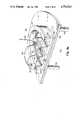
- FIG. 9aillustrates in exploded view a monopole antenna according to an embodiment of the invention.
- a first vertically oriented conductive tube 912has an internal bore dimensioned to fit over a portion of a nonconductive mounting flange 914 arranged for insulated mounting of tube 912 spaced from a ground plane 911.
- Flange 914is bolted to ground plane 911 by bolts, one of which is illustrated as 916.
- Mounting flange 914has a central aperture 918 bored therethrough, through which fiber optic cables, discussed below, can pass to a control source located below ground plane 911.
- a signal sourceenergizes the lower end of tube 912 relative to ground plane 911.
- a further conductive tube 920is mechanically fastened to, but insulated from tube 912 by a nonconductive mounting member 922.
- Nonconductive member 922is illustrated in cross section in FIG. 9b.
- a rigid mechanical mountingis provided by conductive bolts, one of which is illustrated as 930, passing through the walls of the tubes and of dielectric element 922, together with associated nuts (not separately designated).
- electrical connectionis made between lower tube 912 and upper tube 920 by way of a photosensitive conductor arrangement.
- the photosensitive conductor arrangementis illustrated in FIG. 9b.
- each boltsuch as bolt 930, makes contact with the associated tube such as tube 920 and is therefore electrically connected thereto.
- An elongated vertically oriented conductive bar 932is in conductive contact with bolt 930 and is retained in place by a nut 934. Bar 932 extends downward towards tube 912. Other conductive bars 932', 932" are similarly in conductive contact with upper tube 920.
- Another bolt 936is in contact with lower tube 912 and is connected to a bar 938 by a nut 940, establishing conductive contact between bar 938 and lower tube 912.
- Other bars 938', 938"are similarly in contact with lower tube 912. Consequently, representative conductive bars 932 and 938 are available for electrical connection to upper tube 920 and lower tube 912 within annular support 922.
- a packaged semiconductor 942is located within annular support 922 and has leads 943 and 944 connected to bars 932 and 938, respectively.
- a fiber optic cable 946is connected to the photosensitive semiconductor.
- Other packaged semiconductors 948 and 950are connected in parallel with semiconductor 942 and are controlled by other fiber optic cables.
- FIG. 9cis a perspective view illustrating packaged semiconductor 942 in detail. As illustrated, a protective cover has been removed to expose interior details.
- packaged semiconductor 942includes a flat conductive base 952 to which a lead 954 is conductively bonded. A further lead 956 passes through a supporting insulator 958.
- PIN diode 960is mounted on base plate 952.
- Diode 960includes a semiconductor substrate 962 having a conductive layer 964 bonded thereto and to base plate 952.
- diode 960includes a vertically arrayed doping arrangement of a p+ region 966, an i region 968 and an n+region 970. As illustrated in FIG.
- substrate 962 of diode 960is elongated rather than circular in shape, and an elongated moat 972 extends about the diode, separating a central mesa region from an outer periphery of substrate 962.
- the central region of substrate 962includes a trench 974 which passes through p+ region 966 and part-way through i region 968 Contact is made between lead 956 and electrode metallization 976 overlying p+ region 966 in the central mesa region by way of one or more conductors 980, 980'.
- the end of fiber optic cable 946is tapered to a point, and lies in trench 974. Fiber-optic cable 946 is retained in position in trench 974 by adhesive (not illustrated).
- the arrangement of packaged diode 942is an elongated PIN diode in which the light output is distributed along the length of the structure.
- the elongated structuretends to keep the current density at any point within the diode relatively low, and provides low reactance and good heat dissipation capability.
- FIG. 10aillustrates an antenna array according to another embodiment of the invention.
- a semiconductor substrate 1012overlies a ground metallization 1011.
- An array of two antennas 1008 and 1008'is defined by patterns of metallization on, and doping within, semiconductor substrate 1012.
- elements corresponding to elements of antenna 208 of FIG. 2aare designated by the same reference numeral in the 1000 series rather than the 200 series.
- Antenna 1008includes a radiating patch 1010, a further radiation affecting conductor 1014, and a photosensitive element 1030 formed within substrate 1012, coupling together conductor 1014 and a further conductor 1016.
- Conductor 1016is connected by way of a choke 1018 and through conductors (not illustrated) to ground metallization 1011.
- a fiber optic cable 1050has one end adjacent photosensitive element 1030.
- Antenna 1008'is identical to antenna 1008.
- Conductor 1010is connected to a feed conductor 1012, and conductor 1010' is connected to a corresponding feed conductor 1012'.
- Feed conductors 1012 and 1012'are connected together in a common or corporate feed arrangement by a further conductor 1052.
- Electrical biasmay be applied from a bias source illustrated as 1054 by way of a choke illustrated as 1056. It will be noted that the electrical bias applied to conductor 1052 is applied equally to photosensitive elements 1030 and 1030'.
- FIG. 10bis a cross-sectional view of a portion of antenna 1008' looking in the direction 10B--10B.
- substrate 1012is intrinsic (i) semiconductor (semiconductor without significant impurities which affect its conductivity).
- a region 1098 extending under conductor 1014' and into gap 1030'is heavily doped with acceptor impurities to form a p+ region 1098.
- Another region lying under conductor 1016' and extending into gap 1030'is heavily doped with electron donor impurities to form n+ region 1096.
- Regions 1096 and 1098are everywhere separated by i material, thereby defining a lateral PIN diode extending between conductors 1014' and 1016'.
- Fiber optic cable 1050'ends near gap 1030' and is oriented to direct light towards to the junction region between the i region and the adjacent p+ and n+ regions.
- a clear adhesive material or epoxy illustrated as 1094keeps the end of fiber optic cable 1050' in the proper location for illuminating the junction.
- junctions of the diodes 1030, 1030' of antennas 1008 and 1008', respectively, of FIG. 10amay be illuminated with the same amount of light, or the amount of light may be adjusted to compensate for differences in the impedance of the diodes.
- the magnitude of the light applied to diodes 1030, 1030'may be increased or decreased simultaneously so as effect simultaneous tuning of antennas 1008 and 1008' of the array illustrated in FIG. 10a, or they may be selectively illuminated with different amounts of light to change the impedance presented by each antenna at the corporate feed point so as to adjust the reactance and conductance (phase and magnitude) of the feed current entering each antenna to perform beam direction scanning.
- FIGS. 11a and 11billustrate a patch antenna similar to that illustrated in the aforementioned Bhartia et al. patent, modified by the use of glass-encapsulated photosensitive semiconductors. Elements of FIG. 11a and 11b corresponding to FIGS. 1a and 1b are designated by the same reference numeral. As illustrated in FIGS. 11a and 11b, patch antenna 10 has discrete diodes, one of which is designated 15, inserted into holes such as 18 drilled or punched through the structure. In the embodiment of FIGS. 11a and 11b, diode 15 is glass-encapsulated, and the diode structure therein is photosensitive.
- Fiber optic cables 1110 and 1120are connected to a fiber optic star coupler illustrated as 1130 which receives light from a laser light source 1131 and which divides the received light and applies substantially equal amounts of light to cables 1110 and 1120.
- the ends of fiber optic cables 1110 and 1120 remote from star coupler 1130are inserted through skewed holes 1112 and 1122, respectively, to bear against the side of the associated glass-encapsulated diode.
- fiber optic cable 1110passes through skewed hole 1112 and bears against the side of diode 15.
- the fiber optic cablesdo not substantially interfere with the radiation of electromagnetic signals.
- a bead of adhesive illustrated as 1140holds the end of fiber optic cable 1120 in contact with the side of diode 15.
- Such a structureis readily usable with conventional components for achieving frequency, polarization, and other types of diversity as known in the prior art, under the control of light.
- FIG. 12aillustrates in exploded view another embodiment of the invention in which a patch antenna 1208 includes a circular conductive patch 1210 formed on a semiconductor substrate 1212 is coupled by an annular monolithic lateral PIN diode 1250 to a further conductive annulus 1252.
- a truncated conical member 1254is formed from a clear thermoplastic material having a relatively high dielectric constant. Lamps, one of which is illustrated as 1256 in the cross section of FIG. 12b, are embedded in the upper edge of member 1254. The lamps are powered by conductor pairs such as 1258 and together with member 1254 produce an annular ring of light for controlling diode 1250.
- a feed conductor 1298extends through a hole 1296 drilled or punched through conductor 1210 and substrate 1212. Ground plane 1211 defines a clear region around conductor 1298 to prevent short-circuiting thereto. Conductor 1298 is soldered to conductor 1210.
- lamps such as 1256When lamps such as 1256 are illuminated, the light is guided through the lower edge of member 1254 and illuminates the active portion of annular diode 1250, thereby selectively affecting the conduction characteristics of the diode. This in turn controls the coupling of circular patch conductor 1210 to annular conductive patch 1252, thereby in turn affecting the aperture dimensions of patch antenna 1208 and affecting its characteristics.
- FIG. 13is cross-section of an annular patch antenna similar to that illustrated in FIG. 12a, but which provides light to annular diode 1250 by means of a number of fiber optic cables such as 1310, 1320 originating from a star coupler 1330.
- the ends of fiber optic cables 1310 and 1320are fitted into a corresponding set of holes 1311 and 1321 drilled part-way through substrate 1212 from the ground side.
- the ends of fiber optic cables 1310 and 1320direct the light towards annular diode 1250 at sufficient points around the periphery to create a sufficient number of conducting points to simulate a continuous annular connection.
- An advantage of the arrangement of FIG. 13 by comparison with that of FIGS. 12a and 12blies in that radiation of signal from the antenna is not impeded by light distributing structure 1254.
- FIG. 14illustrates in plan view an arrangement of conductive arms 1410, 1420 arranged in the form of an equiangular spiral on the surface of a semiconductor substrate 1412.
- Equiangular spiralsare well known in the art, and are described at Chapter 18.2 of "Antenna Engineering Handbook", first edition, edited by Jasik. As known, such spirals, as with many balanced antenna structures, do not require a ground plane in order to effect radiation.
- Conductive arms 1410 and 1420are fed in balanced form in conventional manner from points 1411, 1421. In accordance with the invention, the impedance presented by arms 1410 and 1420 at feed point 1411, 1421 may be changed by changing the effective width of the arms.
- a further set of conductive spirals 1413 and 1423also have equiangular form, but do not connect directly to feed points 1411, 1421 or to spirals 1410, 1420.
- a distributed lateral PIN diode 1414is formed within the surface of substrate 1412 in the region between spiral arms 1410 and 1413, and a similar distributed lateral PIN diode illustrated as 1424 is formed within the surface of substrate 1412 in the region between conductive spiral arms 1420 and 1423.
- a source of illumination(not illustrated in FIG. 14) controllably illuminates diodes 1414 and 1424 to thereby control the conductive characteristics thereof to control the effective width of the spiral arms and thereby change the impedance of the antenna without changing the radiation characteristic.
- FIG. 15a-15fillustrate steps in the formation of a discrete diode such as diode 230 of FIG. 2c.
- FIG. 15aillustrates an intrinsic (i) semiconductor substrate 1512 which may be Si, GaAs, or other semiconductor material.
- FIG. 15billustrates the result of heavily doping the upper side of substrate 12 with an acceptor impurity such as boron, for a Si substrate and beryllium for a GaAs substrate to form p+ region 1550, and heavily doping the lower side of substrate 1512 with a donor impurity (such as phosphorus for Si and silicon in the case of GaAs) to form n+ region 1554, leaving an intrinsic region 1552 therebetween.
- FIG. 15aillustrates an intrinsic (i) semiconductor substrate 1512 which may be Si, GaAs, or other semiconductor material.
- FIG. 15billustrates the result of heavily doping the upper side of substrate 12 with an acceptor impurity such as boron, for a Si substrate and beryllium for a Ga
- 15cillustrates the result of photolithographic application of a mask 1598 at selected locations on the upper surface of substrate 1512.
- Metalis applied to the unmasked portions of the upper and lower surfaces of substrate 1512, and the mask is removed, thereby leaving a structure such as that illustrated in FIG. 15d, with metallized regions of the upper surface designated 1560 which define a window 1562.
- the upper surface of the structure of FIG. 15dis then masked to leave exposed the regions in which moats are to be formed, and the unmasked regions are etched to form moats illustrated as 1556.
- the substrateis scribed and diced along the dotted lines in FIG. 15e to form the final structure illustrated in FIG. 15f.
- FIG. 16illustrates the result of dividing the above-described etching step into two parts.
- the etchingproceeds to a point at which moats 1556 (FIG. 15e) are partially formed.
- a portion of the mask above window 1562is removed, and the etching is again performed to complete the formation of moats 1556, and to create a shallow depression or trench 1596 below window 1562, thereby creating a location for receiving a fiber optic cable such as those illustrated in FIGS. 8c and 9c.
- the light sourcemay be monochromatic or polychromatic, visible or invisible, coherent or incoherent, and may have its frequency selected for maximum absorption or effect in the photosensitive semiconductor.
- Reflectors or directorsmay be used to direct the light to the appropriate photosensitive elements.
- photosensitive elements or materialmay be used, such as cadmium sulfide (CaS) elements. Doping may or may not be necessary, depending upon the material selected.
- CaScadmium sulfide
- Dopingmay or may not be necessary, depending upon the material selected.
- the low pass filter which applies direct electrical bias to the antenna or its feed linemay be a discrete or a distributed structure, as is known in the filter arts.
- the short-circuiting structure equivalent to solenoidal windings 225 and conductor 218may be implemented as nonsolenoidal conductors in conjunction with quarter-wavelength lengths of transmission line.
Landscapes
- Engineering & Computer Science (AREA)
- Radar, Positioning & Navigation (AREA)
- Remote Sensing (AREA)
- Variable-Direction Aerials And Aerial Arrays (AREA)
- Waveguide Aerials (AREA)
Abstract
Description
Claims (24)
Priority Applications (1)
| Application Number | Priority Date | Filing Date | Title |
|---|---|---|---|
| US06/858,771US4751513A (en) | 1986-05-02 | 1986-05-02 | Light controlled antennas |
Applications Claiming Priority (1)
| Application Number | Priority Date | Filing Date | Title |
|---|---|---|---|
| US06/858,771US4751513A (en) | 1986-05-02 | 1986-05-02 | Light controlled antennas |
Publications (1)
| Publication Number | Publication Date |
|---|---|
| US4751513Atrue US4751513A (en) | 1988-06-14 |
Family
ID=25329131
Family Applications (1)
| Application Number | Title | Priority Date | Filing Date |
|---|---|---|---|
| US06/858,771Expired - Fee RelatedUS4751513A (en) | 1986-05-02 | 1986-05-02 | Light controlled antennas |
Country Status (1)
| Country | Link |
|---|---|
| US (1) | US4751513A (en) |
Cited By (72)
| Publication number | Priority date | Publication date | Assignee | Title |
|---|---|---|---|---|
| US4855749A (en)* | 1988-02-26 | 1989-08-08 | The United States Of America As Represented By The Secretary Of The Air Force | Opto-electronic vivaldi transceiver |
| US5155493A (en)* | 1990-08-28 | 1992-10-13 | The United States Of America As Represented By The Secretary Of The Air Force | Tape type microstrip patch antenna |
| EP0524878A1 (en)* | 1991-07-25 | 1993-01-27 | Commissariat A L'energie Atomique | Microwave semiconductor absorber with optical command |
| US5309163A (en)* | 1991-09-12 | 1994-05-03 | Trw Inc. | Active patch antenna transmitter |
| US5367310A (en)* | 1991-10-11 | 1994-11-22 | Southwest Research Institute | Fiber optic antenna radiation efficiency tuner |
| AU655953B2 (en)* | 1990-12-14 | 1995-01-19 | Aisin Seiki Kabushiki Kaisha | Microstrip antenna |
| US5481232A (en)* | 1995-04-19 | 1996-01-02 | New Jersey Institute Of Technology | Optically controlled multilayer coplanar waveguide phase shifter |
| US5497165A (en)* | 1990-12-14 | 1996-03-05 | Aisin Seiki Kabushiki Kaisha | Microstrip antenna |
| US5754143A (en)* | 1996-10-29 | 1998-05-19 | Southwest Research Institute | Switch-tuned meandered-slot antenna |
| US5777581A (en)* | 1995-12-07 | 1998-07-07 | Atlantic Aerospace Electronics Corporation | Tunable microstrip patch antennas |
| WO1998035402A1 (en)* | 1997-02-07 | 1998-08-13 | Thomson-Csf | Antenna with variable geometry |
| FR2759497A1 (en)* | 1997-02-07 | 1998-08-14 | Thomson Csf | Variable geometry antenna for frequencies below 1GHz |
| US5943016A (en)* | 1995-12-07 | 1999-08-24 | Atlantic Aerospace Electronics, Corp. | Tunable microstrip patch antenna and feed network therefor |
| US6049308A (en)* | 1997-03-27 | 2000-04-11 | Sandia Corporation | Integrated resonant tunneling diode based antenna |
| US6061025A (en)* | 1995-12-07 | 2000-05-09 | Atlantic Aerospace Electronics Corporation | Tunable microstrip patch antenna and control system therefor |
| US6069587A (en)* | 1998-05-15 | 2000-05-30 | Hughes Electronics Corporation | Multiband millimeterwave reconfigurable antenna using RF mem switches |
| US6078288A (en)* | 1997-11-21 | 2000-06-20 | Lockheed Martin Corporation | Photonically controlled antenna array |
| US6175332B1 (en)* | 1997-09-16 | 2001-01-16 | The United States Of America As Represented By The Secretary Of The Air Force | Diffractive beam forming and scanning antenna array |
| US6396046B1 (en)* | 1999-11-02 | 2002-05-28 | General Electric Company | Imager with reduced FET photoresponse and high integrity contact via |
| WO2002075845A1 (en)* | 2001-03-15 | 2002-09-26 | Filtronic Lk Oy | Adjustable antenna |
| US6473042B1 (en)* | 2001-04-11 | 2002-10-29 | Acer Neweb Corporation | Antenna for an electronic device |
| WO2003030301A1 (en)* | 2001-10-01 | 2003-04-10 | Raytheon Company | Slot coupled, polarized radiator |
| US20030112186A1 (en)* | 2001-09-19 | 2003-06-19 | Sanchez Victor C. | Broadband antennas over electronically reconfigurable artificial magnetic conductor surfaces |
| US6590150B1 (en) | 2001-05-11 | 2003-07-08 | Karl F. Kiefer | Combination photovoltaic cell and RF antenna and method |
| WO2003065499A2 (en) | 2002-01-28 | 2003-08-07 | Nokia Corporation | Tunable antenna for wireless communication terminals |
| US6617670B2 (en)* | 2000-03-20 | 2003-09-09 | Sarnoff Corporation | Surface PIN device |
| US6643418B2 (en)* | 2000-06-30 | 2003-11-04 | Alcatel | Electric or opto-electric component with a packaging of plastic and a method for varying the impedance of a terminal lead of the component by attaching a dielectric plate to at least one terminal lead |
| US6707429B1 (en)* | 2002-12-09 | 2004-03-16 | The United States Of America As Represented By The Administrator Of The National Aeronautics And Space Administration | Self-contained sub-millimeter wave rectifying antenna integrated circuit |
| US20040113842A1 (en)* | 2002-08-15 | 2004-06-17 | Du Toit Cornelis Frederik | Conformal frequency-agile tunable patch antenna |
| US6897831B2 (en)* | 2001-04-30 | 2005-05-24 | Titan Aerospace Electronic Division | Reconfigurable artificial magnetic conductor |
| US20050119035A1 (en)* | 2002-09-26 | 2005-06-02 | Kentaro Miyano | Radio terminal device antenna and radio terminal device |
| EP1617511A1 (en)* | 2004-07-12 | 2006-01-18 | Lockheed Martin Corporation | RF antenna array structure |
| US20060097849A1 (en)* | 1997-08-18 | 2006-05-11 | Dando Ross S | Wireless communication devices and methods of forming and operating the same |
| US7106201B2 (en)* | 1997-08-20 | 2006-09-12 | Micron Technology, Inc. | Communication devices, remote intelligent communication devices, electronic communication devices, methods of forming remote intelligent communication devices and methods of forming a radio frequency identification device |
| US20070274642A1 (en)* | 2006-04-12 | 2007-11-29 | Fujifilm Corporation | Optical transmission system |
| US20080129630A1 (en)* | 2002-09-10 | 2008-06-05 | Carles Puente Baliarda | Coupled multiband antennas |
| US20080217538A1 (en)* | 2004-07-30 | 2008-09-11 | Canon Kabushiki Kaisha | Optical Semiconductor Device |
| US20080265038A1 (en)* | 2004-07-23 | 2008-10-30 | Fractus, S.A. | Antenna in Package with Reduced Electromagnetic Interaction with on Chip Elements |
| US20090085810A1 (en)* | 2002-11-07 | 2009-04-02 | Fractus, S.A. | Integrated circuit package including miniature antenna |
| NL2001938C2 (en)* | 2008-08-29 | 2009-08-03 | Cyner Substrates B V | Antenna device for use in mobile telecommunication applications, has antenna element having connecting electrode that is coupled for electrical conduction to electric port of electro-optical converter |
| US7583192B2 (en) | 1992-08-12 | 2009-09-01 | Keystone Technology Solutions, Llc | Radio frequency identification device and method |
| US20100066631A1 (en)* | 2006-09-21 | 2010-03-18 | Raytheon Company | Panel Array |
| US20100126010A1 (en)* | 2006-09-21 | 2010-05-27 | Raytheon Company | Radio Frequency Interconnect Circuits and Techniques |
| US20100245179A1 (en)* | 2009-03-24 | 2010-09-30 | Raytheon Company | Method and Apparatus for Thermal Management of a Radio Frequency System |
| US20100253583A1 (en)* | 2008-01-07 | 2010-10-07 | Fujitsu Limited | Electronic device, antenna and article |
| US20110075377A1 (en)* | 2009-09-25 | 2011-03-31 | Raytheon Copany | Heat Sink Interface Having Three-Dimensional Tolerance Compensation |
| WO2012100885A1 (en)* | 2011-01-25 | 2012-08-02 | Sony Corporation | Optically controlled microwave antenna |
| US8355255B2 (en) | 2010-12-22 | 2013-01-15 | Raytheon Company | Cooling of coplanar active circuits |
| US8363413B2 (en) | 2010-09-13 | 2013-01-29 | Raytheon Company | Assembly to provide thermal cooling |
| US20130038138A1 (en)* | 2008-01-14 | 2013-02-14 | Qualcomm Incorporated | Wireless powering and charging station |
| US8427371B2 (en) | 2010-04-09 | 2013-04-23 | Raytheon Company | RF feed network for modular active aperture electronically steered arrays |
| US8508943B2 (en) | 2009-10-16 | 2013-08-13 | Raytheon Company | Cooling active circuits |
| US8810448B1 (en) | 2010-11-18 | 2014-08-19 | Raytheon Company | Modular architecture for scalable phased array radars |
| US8922454B2 (en) | 2010-03-24 | 2014-12-30 | Mina Danesh | Integrated photovoltaic cell and radio-frequency antenna |
| US9019166B2 (en) | 2009-06-15 | 2015-04-28 | Raytheon Company | Active electronically scanned array (AESA) card |
| US20150180122A1 (en)* | 2013-12-24 | 2015-06-25 | The Boeing Company | Integral rf-optical phased array module |
| US20150222019A1 (en)* | 2014-02-04 | 2015-08-06 | Raytheon Company | Optically reconfigurable rf fabric |
| US9124361B2 (en) | 2011-10-06 | 2015-09-01 | Raytheon Company | Scalable, analog monopulse network |
| US9130278B2 (en) | 2012-11-26 | 2015-09-08 | Raytheon Company | Dual linear and circularly polarized patch radiator |
| US20150280448A1 (en)* | 2014-03-31 | 2015-10-01 | Qualcomm Incorporated | Systems, apparatus, and methods for wireless power receiver coil configuration |
| US9172145B2 (en) | 2006-09-21 | 2015-10-27 | Raytheon Company | Transmit/receive daughter card with integral circulator |
| US9407976B2 (en) | 2014-02-04 | 2016-08-02 | Raytheon Company | Photonically routed transmission line |
| US9639001B2 (en) | 2014-02-04 | 2017-05-02 | Raytheon Company | Optically transitioned metal-insulator surface |
| US9728668B2 (en) | 2014-02-04 | 2017-08-08 | Raytheon Company | Integrated photosensitive film and thin LED display |
| US20170301636A1 (en)* | 2016-04-14 | 2017-10-19 | Freescale Semiconductor, Inc. | Electrostatic discharge protection for antenna using vias |
| US20180342471A1 (en)* | 2017-05-24 | 2018-11-29 | Advanced Semiconductor Engineering, Inc. | Semiconductor package device |
| CN114188707A (en)* | 2022-02-17 | 2022-03-15 | 荣耀终端有限公司 | Terminal antenna and method for controlling antenna beam direction |
| US20220336965A1 (en)* | 2021-04-20 | 2022-10-20 | Apple Inc. | Electronic Devices Having Bi-Directional Dielectric Resonator Antennas |
| WO2024000306A1 (en)* | 2022-06-29 | 2024-01-04 | 京东方科技集团股份有限公司 | Tunable antenna, preparation method for tunable antenna, and electronic device |
| WO2024262097A1 (en)* | 2023-06-19 | 2024-12-26 | パナソニックIpマネジメント株式会社 | Reflection unit, antenna unit, reflection plate device, and array antenna device |
| US12294160B2 (en) | 2020-12-30 | 2025-05-06 | Instituto Tecnológico Metropolitano | Light-tuned antenna device |
| CN120254814A (en)* | 2025-05-29 | 2025-07-04 | 杭州市北京航空航天大学国际创新研究院(北京航空航天大学国际创新学院) | A radar array device and method based on on-chip antenna-pulse source integration |
Citations (19)
| Publication number | Priority date | Publication date | Assignee | Title |
|---|---|---|---|---|
| US3680136A (en)* | 1971-10-20 | 1972-07-25 | Us Navy | Current sheet antenna |
| US3917943A (en)* | 1974-11-21 | 1975-11-04 | Bell Telephone Labor Inc | Picosecond semiconductor electronic switch controlled by optical means |
| US4053895A (en)* | 1976-11-24 | 1977-10-11 | The United States Of America As Represented By The Secretary Of The Air Force | Electronically scanned microstrip antenna array |
| US4231049A (en)* | 1977-11-10 | 1980-10-28 | Thomson-Csf | Heterojunction photodiode of the avalanche type |
| US4259670A (en)* | 1978-05-16 | 1981-03-31 | Ball Corporation | Broadband microstrip antenna with automatically progressively shortened resonant dimensions with respect to increasing frequency of operation |
| US4281253A (en)* | 1978-08-29 | 1981-07-28 | Optelecom, Inc. | Applications of dual function electro-optic transducer in optical signal transmission |
| US4326771A (en)* | 1979-10-05 | 1982-04-27 | Thomson-Csf | Method of coupling between an optical fiber and an optoelectronic diode, and a transmitting or receiving head fabricated by means of said method |
| US4367474A (en)* | 1980-08-05 | 1983-01-04 | The United States Of America As Represented By The Secretary Of The Army | Frequency-agile, polarization diverse microstrip antennas and frequency scanned arrays |
| US4368481A (en)* | 1979-06-19 | 1983-01-11 | Tokyo Shibaura Denki Kabushiki Kaisha | Light-driven semiconductor device |
| US4376285A (en)* | 1980-06-23 | 1983-03-08 | Massachusetts Institute Of Technology | High speed optoelectronic switch |
| US4379296A (en)* | 1980-10-20 | 1983-04-05 | The United States Of America As Represented By The Secretary Of The Army | Selectable-mode microstrip antenna and selectable-mode microstrip antenna arrays |
| US4382261A (en)* | 1980-05-05 | 1983-05-03 | The United States Of America As Represented By The Secretary Of The Army | Phase shifter and line scanner for phased array applications |
| US4386357A (en)* | 1981-05-21 | 1983-05-31 | Martin Marietta Corporation | Patch antenna having tuning means for improved performance |
| US4388633A (en)* | 1980-09-29 | 1983-06-14 | Hughes Aircraft Company | Monolithic transistor coupled electroluminescent diode |
| US4396833A (en)* | 1981-01-22 | 1983-08-02 | Harris Corporation | Optomicrowave integrated circuit |
| US4399453A (en)* | 1981-03-23 | 1983-08-16 | Motorola, Inc. | Low thermal impedance plastic package |
| US4475108A (en)* | 1982-08-04 | 1984-10-02 | Allied Corporation | Electronically tunable microstrip antenna |
| US4490721A (en)* | 1980-11-17 | 1984-12-25 | Ball Corporation | Monolithic microwave integrated circuit with integral array antenna |
| US4529987A (en)* | 1982-05-13 | 1985-07-16 | Her Majesty The Queen In Right Of Canada, As Represented By The Minister Of National Defence Of Her Majesty's Canadian Government | Broadband microstrip antennas with varactor diodes |
- 1986
- 1986-05-02USUS06/858,771patent/US4751513A/ennot_activeExpired - Fee Related
Patent Citations (19)
| Publication number | Priority date | Publication date | Assignee | Title |
|---|---|---|---|---|
| US3680136A (en)* | 1971-10-20 | 1972-07-25 | Us Navy | Current sheet antenna |
| US3917943A (en)* | 1974-11-21 | 1975-11-04 | Bell Telephone Labor Inc | Picosecond semiconductor electronic switch controlled by optical means |
| US4053895A (en)* | 1976-11-24 | 1977-10-11 | The United States Of America As Represented By The Secretary Of The Air Force | Electronically scanned microstrip antenna array |
| US4231049A (en)* | 1977-11-10 | 1980-10-28 | Thomson-Csf | Heterojunction photodiode of the avalanche type |
| US4259670A (en)* | 1978-05-16 | 1981-03-31 | Ball Corporation | Broadband microstrip antenna with automatically progressively shortened resonant dimensions with respect to increasing frequency of operation |
| US4281253A (en)* | 1978-08-29 | 1981-07-28 | Optelecom, Inc. | Applications of dual function electro-optic transducer in optical signal transmission |
| US4368481A (en)* | 1979-06-19 | 1983-01-11 | Tokyo Shibaura Denki Kabushiki Kaisha | Light-driven semiconductor device |
| US4326771A (en)* | 1979-10-05 | 1982-04-27 | Thomson-Csf | Method of coupling between an optical fiber and an optoelectronic diode, and a transmitting or receiving head fabricated by means of said method |
| US4382261A (en)* | 1980-05-05 | 1983-05-03 | The United States Of America As Represented By The Secretary Of The Army | Phase shifter and line scanner for phased array applications |
| US4376285A (en)* | 1980-06-23 | 1983-03-08 | Massachusetts Institute Of Technology | High speed optoelectronic switch |
| US4367474A (en)* | 1980-08-05 | 1983-01-04 | The United States Of America As Represented By The Secretary Of The Army | Frequency-agile, polarization diverse microstrip antennas and frequency scanned arrays |
| US4388633A (en)* | 1980-09-29 | 1983-06-14 | Hughes Aircraft Company | Monolithic transistor coupled electroluminescent diode |
| US4379296A (en)* | 1980-10-20 | 1983-04-05 | The United States Of America As Represented By The Secretary Of The Army | Selectable-mode microstrip antenna and selectable-mode microstrip antenna arrays |
| US4490721A (en)* | 1980-11-17 | 1984-12-25 | Ball Corporation | Monolithic microwave integrated circuit with integral array antenna |
| US4396833A (en)* | 1981-01-22 | 1983-08-02 | Harris Corporation | Optomicrowave integrated circuit |
| US4399453A (en)* | 1981-03-23 | 1983-08-16 | Motorola, Inc. | Low thermal impedance plastic package |
| US4386357A (en)* | 1981-05-21 | 1983-05-31 | Martin Marietta Corporation | Patch antenna having tuning means for improved performance |
| US4529987A (en)* | 1982-05-13 | 1985-07-16 | Her Majesty The Queen In Right Of Canada, As Represented By The Minister Of National Defence Of Her Majesty's Canadian Government | Broadband microstrip antennas with varactor diodes |
| US4475108A (en)* | 1982-08-04 | 1984-10-02 | Allied Corporation | Electronically tunable microstrip antenna |
Non-Patent Citations (10)
| Title |
|---|
| A paper entitled "Optical Control of Microwave PIN Diode and its Applications" by Sykes et al.; May 2, 1985. |
| A paper entitled Optical Control of Microwave PIN Diode and its Applications by Sykes et al.; May 2, 1985.* |
| An article entitled "High Power Low-Loss PIN Diodes for Phased-Array Radar" by Rosen et al., published in RCA Review, Mar. 1979. |
| An article entitled "Millimeter Wave Silicon Device and Integrated Circuit Technology" by Stabile et al., published in 1984 IEEE MTT-S International Microwave Symposium. |
| An article entitled "Optoelectronically Pulsed Slot-Line Antennas" by Heidemann et al. published in Electronic Letters, Apr. 28, 1983, vol. 19, No. 9. |
| An article entitled High Power Low Loss PIN Diodes for Phased Array Radar by Rosen et al., published in RCA Review, Mar. 1979.* |
| An article entitled Millimeter Wave Silicon Device and Integrated Circuit Technology by Stabile et al., published in 1984 IEEE MTT S International Microwave Symposium.* |
| An article entitled Optoelectronically Pulsed Slot Line Antennas by Heidemann et al. published in Electronic Letters, Apr. 28, 1983, vol. 19, No. 9.* |
| Herczfeld et al.; "Optically Controlled Microwave Devices and Circuits"; RCA Reviews vol. 46; Dec. 1985, pp. 528-551. |
| Herczfeld et al.; Optically Controlled Microwave Devices and Circuits ; RCA Reviews vol. 46; Dec. 1985, pp. 528 551.* |
Cited By (123)
| Publication number | Priority date | Publication date | Assignee | Title |
|---|---|---|---|---|
| US4855749A (en)* | 1988-02-26 | 1989-08-08 | The United States Of America As Represented By The Secretary Of The Air Force | Opto-electronic vivaldi transceiver |
| US5155493A (en)* | 1990-08-28 | 1992-10-13 | The United States Of America As Represented By The Secretary Of The Air Force | Tape type microstrip patch antenna |
| AU655953B2 (en)* | 1990-12-14 | 1995-01-19 | Aisin Seiki Kabushiki Kaisha | Microstrip antenna |
| US5497165A (en)* | 1990-12-14 | 1996-03-05 | Aisin Seiki Kabushiki Kaisha | Microstrip antenna |
| EP0524878A1 (en)* | 1991-07-25 | 1993-01-27 | Commissariat A L'energie Atomique | Microwave semiconductor absorber with optical command |
| FR2679703A1 (en)* | 1991-07-25 | 1993-01-29 | Commissariat Energie Atomique | SEMICONDUCTOR HYPERFREQUENCY DEVICE WITH OPTICAL CONTROL. |
| US5309163A (en)* | 1991-09-12 | 1994-05-03 | Trw Inc. | Active patch antenna transmitter |
| US5367310A (en)* | 1991-10-11 | 1994-11-22 | Southwest Research Institute | Fiber optic antenna radiation efficiency tuner |
| US7583192B2 (en) | 1992-08-12 | 2009-09-01 | Keystone Technology Solutions, Llc | Radio frequency identification device and method |
| US8018340B2 (en) | 1992-08-12 | 2011-09-13 | Round Rock Research, Llc | System and method to track articles at a point of origin and at a point of destination using RFID |
| US7746230B2 (en) | 1992-08-12 | 2010-06-29 | Round Rock Research, Llc | Radio frequency identification device and method |
| US5481232A (en)* | 1995-04-19 | 1996-01-02 | New Jersey Institute Of Technology | Optically controlled multilayer coplanar waveguide phase shifter |
| US5777581A (en)* | 1995-12-07 | 1998-07-07 | Atlantic Aerospace Electronics Corporation | Tunable microstrip patch antennas |
| US5943016A (en)* | 1995-12-07 | 1999-08-24 | Atlantic Aerospace Electronics, Corp. | Tunable microstrip patch antenna and feed network therefor |
| US6061025A (en)* | 1995-12-07 | 2000-05-09 | Atlantic Aerospace Electronics Corporation | Tunable microstrip patch antenna and control system therefor |
| US5754143A (en)* | 1996-10-29 | 1998-05-19 | Southwest Research Institute | Switch-tuned meandered-slot antenna |
| FR2759497A1 (en)* | 1997-02-07 | 1998-08-14 | Thomson Csf | Variable geometry antenna for frequencies below 1GHz |
| FR2759498A1 (en)* | 1997-02-07 | 1998-08-14 | Thomson Csf | VARIABLE GEOMETRY ANTENNA |
| WO1998035402A1 (en)* | 1997-02-07 | 1998-08-13 | Thomson-Csf | Antenna with variable geometry |
| US6195065B1 (en)* | 1997-02-07 | 2001-02-27 | Thomson-Csf | Antenna with variable geometry |
| US6049308A (en)* | 1997-03-27 | 2000-04-11 | Sandia Corporation | Integrated resonant tunneling diode based antenna |
| US20060097849A1 (en)* | 1997-08-18 | 2006-05-11 | Dando Ross S | Wireless communication devices and methods of forming and operating the same |
| US7948382B2 (en) | 1997-08-20 | 2011-05-24 | Round Rock Research, Llc | Electronic communication devices, methods of forming electrical communication devices, and communications methods |
| US7839285B2 (en) | 1997-08-20 | 2010-11-23 | Round Rock Resarch, LLC | Electronic communication devices, methods of forming electrical communication devices, and communications methods |
| US20070007345A1 (en)* | 1997-08-20 | 2007-01-11 | Tuttle Mark E | Electronic communication devices, methods of forming electrical communication devices, and communications methods |
| US7106201B2 (en)* | 1997-08-20 | 2006-09-12 | Micron Technology, Inc. | Communication devices, remote intelligent communication devices, electronic communication devices, methods of forming remote intelligent communication devices and methods of forming a radio frequency identification device |
| US6175332B1 (en)* | 1997-09-16 | 2001-01-16 | The United States Of America As Represented By The Secretary Of The Air Force | Diffractive beam forming and scanning antenna array |
| US6078288A (en)* | 1997-11-21 | 2000-06-20 | Lockheed Martin Corporation | Photonically controlled antenna array |
| US6069587A (en)* | 1998-05-15 | 2000-05-30 | Hughes Electronics Corporation | Multiband millimeterwave reconfigurable antenna using RF mem switches |
| US6396046B1 (en)* | 1999-11-02 | 2002-05-28 | General Electric Company | Imager with reduced FET photoresponse and high integrity contact via |
| US6617670B2 (en)* | 2000-03-20 | 2003-09-09 | Sarnoff Corporation | Surface PIN device |
| US6643418B2 (en)* | 2000-06-30 | 2003-11-04 | Alcatel | Electric or opto-electric component with a packaging of plastic and a method for varying the impedance of a terminal lead of the component by attaching a dielectric plate to at least one terminal lead |
| US20040233108A1 (en)* | 2001-03-15 | 2004-11-25 | Mika Bordi | Adjustable antenna |
| US6856293B2 (en) | 2001-03-15 | 2005-02-15 | Filtronic Lk Oy | Adjustable antenna |
| WO2002075845A1 (en)* | 2001-03-15 | 2002-09-26 | Filtronic Lk Oy | Adjustable antenna |
| US6473042B1 (en)* | 2001-04-11 | 2002-10-29 | Acer Neweb Corporation | Antenna for an electronic device |
| US6897831B2 (en)* | 2001-04-30 | 2005-05-24 | Titan Aerospace Electronic Division | Reconfigurable artificial magnetic conductor |
| US6590150B1 (en) | 2001-05-11 | 2003-07-08 | Karl F. Kiefer | Combination photovoltaic cell and RF antenna and method |
| US20030112186A1 (en)* | 2001-09-19 | 2003-06-19 | Sanchez Victor C. | Broadband antennas over electronically reconfigurable artificial magnetic conductor surfaces |
| US6917343B2 (en) | 2001-09-19 | 2005-07-12 | Titan Aerospace Electronics Division | Broadband antennas over electronically reconfigurable artificial magnetic conductor surfaces |
| WO2003030301A1 (en)* | 2001-10-01 | 2003-04-10 | Raytheon Company | Slot coupled, polarized radiator |
| EP1764863A1 (en)* | 2001-10-01 | 2007-03-21 | Raython Company | Slot coupled, polarized radiator |
| US6624787B2 (en) | 2001-10-01 | 2003-09-23 | Raytheon Company | Slot coupled, polarized, egg-crate radiator |
| WO2003065499A2 (en) | 2002-01-28 | 2003-08-07 | Nokia Corporation | Tunable antenna for wireless communication terminals |
| EP1470611A4 (en)* | 2002-01-28 | 2006-06-07 | Nokia Corp | TUNABLE ANTENNA FOR WIRELESS COMMUNICATION TERMINALS |
| CN100380735C (en)* | 2002-01-28 | 2008-04-09 | 诺基亚有限公司 | Tunable Antennas for Wireless Communication Terminals |
| EP2079129A1 (en)* | 2002-01-28 | 2009-07-15 | Nokia Corporation | Tunable antenna for wireless communication terminals |
| US20040113842A1 (en)* | 2002-08-15 | 2004-06-17 | Du Toit Cornelis Frederik | Conformal frequency-agile tunable patch antenna |
| US6864843B2 (en)* | 2002-08-15 | 2005-03-08 | Paratek Microwave, Inc. | Conformal frequency-agile tunable patch antenna |
| US8994604B2 (en) | 2002-09-10 | 2015-03-31 | Fractus, S.A. | Coupled multiband antennas |
| US10468770B2 (en) | 2002-09-10 | 2019-11-05 | Fractus, S.A. | Coupled multiband antennas |
| US20080129630A1 (en)* | 2002-09-10 | 2008-06-05 | Carles Puente Baliarda | Coupled multiband antennas |
| US10734723B2 (en) | 2002-09-10 | 2020-08-04 | Fractus, S. A. | Couple multiband antennas |
| US10135138B2 (en) | 2002-09-10 | 2018-11-20 | Fractus, S.A. | Coupled multiband antennas |
| US20050119035A1 (en)* | 2002-09-26 | 2005-06-02 | Kentaro Miyano | Radio terminal device antenna and radio terminal device |
| US7212164B2 (en)* | 2002-09-26 | 2007-05-01 | Matsushita Electric Industrial Co., Ltd. | Radio terminal device antenna and radio terminal device |
| US10320079B2 (en) | 2002-11-07 | 2019-06-11 | Fractus, S.A. | Integrated circuit package including miniature antenna |
| US20090085810A1 (en)* | 2002-11-07 | 2009-04-02 | Fractus, S.A. | Integrated circuit package including miniature antenna |
| US8421686B2 (en)* | 2002-11-07 | 2013-04-16 | Fractus, S.A. | Radio-frequency system in package including antenna |
| US10644405B2 (en) | 2002-11-07 | 2020-05-05 | Fractus, S.A. | Integrated circuit package including miniature antenna |
| US9077073B2 (en) | 2002-11-07 | 2015-07-07 | Fractus, S.A. | Integrated circuit package including miniature antenna |
| US9761948B2 (en) | 2002-11-07 | 2017-09-12 | Fractus, S.A. | Integrated circuit package including miniature antenna |
| US20100328185A1 (en)* | 2002-11-07 | 2010-12-30 | Jordi Soler Castany | Radio-frequency system in package including antenna |
| US10056691B2 (en) | 2002-11-07 | 2018-08-21 | Fractus, S.A. | Integrated circuit package including miniature antenna |
| US8203488B2 (en) | 2002-11-07 | 2012-06-19 | Fractus, S.A. | Integrated circuit package including miniature antenna |
| US6707429B1 (en)* | 2002-12-09 | 2004-03-16 | The United States Of America As Represented By The Administrator Of The National Aeronautics And Space Administration | Self-contained sub-millimeter wave rectifying antenna integrated circuit |
| US7023390B1 (en) | 2004-07-12 | 2006-04-04 | Lockheed Martin Corporation | RF antenna array structure |
| EP1617511A1 (en)* | 2004-07-12 | 2006-01-18 | Lockheed Martin Corporation | RF antenna array structure |
| US8330259B2 (en) | 2004-07-23 | 2012-12-11 | Fractus, S.A. | Antenna in package with reduced electromagnetic interaction with on chip elements |
| US20080265038A1 (en)* | 2004-07-23 | 2008-10-30 | Fractus, S.A. | Antenna in Package with Reduced Electromagnetic Interaction with on Chip Elements |
| US7723708B2 (en)* | 2004-07-30 | 2010-05-25 | Canon Kabushiki Kaisha | Optical semiconductor device in which an electromagnetic wave is generated in a region of an applied electric field |
| US20080217538A1 (en)* | 2004-07-30 | 2008-09-11 | Canon Kabushiki Kaisha | Optical Semiconductor Device |
| US20070274642A1 (en)* | 2006-04-12 | 2007-11-29 | Fujifilm Corporation | Optical transmission system |
| US8981869B2 (en) | 2006-09-21 | 2015-03-17 | Raytheon Company | Radio frequency interconnect circuits and techniques |
| US8279131B2 (en) | 2006-09-21 | 2012-10-02 | Raytheon Company | Panel array |
| US20100066631A1 (en)* | 2006-09-21 | 2010-03-18 | Raytheon Company | Panel Array |
| US9172145B2 (en) | 2006-09-21 | 2015-10-27 | Raytheon Company | Transmit/receive daughter card with integral circulator |
| US20100126010A1 (en)* | 2006-09-21 | 2010-05-27 | Raytheon Company | Radio Frequency Interconnect Circuits and Techniques |
| US20100253583A1 (en)* | 2008-01-07 | 2010-10-07 | Fujitsu Limited | Electronic device, antenna and article |
| US8188931B2 (en)* | 2008-01-07 | 2012-05-29 | Fujitsu Limited | Electronic device, antenna and article |
| US20130038138A1 (en)* | 2008-01-14 | 2013-02-14 | Qualcomm Incorporated | Wireless powering and charging station |
| NL2001938C2 (en)* | 2008-08-29 | 2009-08-03 | Cyner Substrates B V | Antenna device for use in mobile telecommunication applications, has antenna element having connecting electrode that is coupled for electrical conduction to electric port of electro-optical converter |
| US7859835B2 (en) | 2009-03-24 | 2010-12-28 | Allegro Microsystems, Inc. | Method and apparatus for thermal management of a radio frequency system |
| US20100245179A1 (en)* | 2009-03-24 | 2010-09-30 | Raytheon Company | Method and Apparatus for Thermal Management of a Radio Frequency System |
| US9019166B2 (en) | 2009-06-15 | 2015-04-28 | Raytheon Company | Active electronically scanned array (AESA) card |
| US8537552B2 (en) | 2009-09-25 | 2013-09-17 | Raytheon Company | Heat sink interface having three-dimensional tolerance compensation |
| US20110075377A1 (en)* | 2009-09-25 | 2011-03-31 | Raytheon Copany | Heat Sink Interface Having Three-Dimensional Tolerance Compensation |
| US8508943B2 (en) | 2009-10-16 | 2013-08-13 | Raytheon Company | Cooling active circuits |
| US8922454B2 (en) | 2010-03-24 | 2014-12-30 | Mina Danesh | Integrated photovoltaic cell and radio-frequency antenna |
| US8427371B2 (en) | 2010-04-09 | 2013-04-23 | Raytheon Company | RF feed network for modular active aperture electronically steered arrays |
| US8363413B2 (en) | 2010-09-13 | 2013-01-29 | Raytheon Company | Assembly to provide thermal cooling |
| US9116222B1 (en) | 2010-11-18 | 2015-08-25 | Raytheon Company | Modular architecture for scalable phased array radars |
| US8810448B1 (en) | 2010-11-18 | 2014-08-19 | Raytheon Company | Modular architecture for scalable phased array radars |
| US8355255B2 (en) | 2010-12-22 | 2013-01-15 | Raytheon Company | Cooling of coplanar active circuits |
| US9496610B2 (en) | 2011-01-25 | 2016-11-15 | Sony Corporation | Optically controlled microwave antenna |
| WO2012100885A1 (en)* | 2011-01-25 | 2012-08-02 | Sony Corporation | Optically controlled microwave antenna |
| US9124361B2 (en) | 2011-10-06 | 2015-09-01 | Raytheon Company | Scalable, analog monopulse network |
| US9397766B2 (en) | 2011-10-06 | 2016-07-19 | Raytheon Company | Calibration system and technique for a scalable, analog monopulse network |
| US9130278B2 (en) | 2012-11-26 | 2015-09-08 | Raytheon Company | Dual linear and circularly polarized patch radiator |
| US9595757B2 (en)* | 2013-12-24 | 2017-03-14 | The Boeing Company | Integral RF-optical phased array module |
| US20150180122A1 (en)* | 2013-12-24 | 2015-06-25 | The Boeing Company | Integral rf-optical phased array module |
| US9728668B2 (en) | 2014-02-04 | 2017-08-08 | Raytheon Company | Integrated photosensitive film and thin LED display |
| US9639001B2 (en) | 2014-02-04 | 2017-05-02 | Raytheon Company | Optically transitioned metal-insulator surface |
| US9985166B2 (en) | 2014-02-04 | 2018-05-29 | Raytheon Company | Integrated photosensitive film and thin LED display |
| US9437921B2 (en)* | 2014-02-04 | 2016-09-06 | Raytheon Company | Optically reconfigurable RF fabric |
| US20150222019A1 (en)* | 2014-02-04 | 2015-08-06 | Raytheon Company | Optically reconfigurable rf fabric |
| US9407976B2 (en) | 2014-02-04 | 2016-08-02 | Raytheon Company | Photonically routed transmission line |
| US10461582B2 (en)* | 2014-03-31 | 2019-10-29 | Qualcomm Incorporated | Systems, apparatus, and methods for wireless power receiver coil configuration |
| US20150280448A1 (en)* | 2014-03-31 | 2015-10-01 | Qualcomm Incorporated | Systems, apparatus, and methods for wireless power receiver coil configuration |
| US20170301636A1 (en)* | 2016-04-14 | 2017-10-19 | Freescale Semiconductor, Inc. | Electrostatic discharge protection for antenna using vias |
| US10115683B2 (en)* | 2016-04-14 | 2018-10-30 | Nxp Usa, Inc. | Electrostatic discharge protection for antenna using vias |
| US10546825B2 (en) | 2017-05-24 | 2020-01-28 | Advanced Semiconductor Engineering, Inc. | Semiconductor package device |
| US10199336B2 (en)* | 2017-05-24 | 2019-02-05 | Advanced Semiconductor Engineering, Inc. | Antenna package device |
| US20180342471A1 (en)* | 2017-05-24 | 2018-11-29 | Advanced Semiconductor Engineering, Inc. | Semiconductor package device |
| US12294160B2 (en) | 2020-12-30 | 2025-05-06 | Instituto Tecnológico Metropolitano | Light-tuned antenna device |
| US20220336965A1 (en)* | 2021-04-20 | 2022-10-20 | Apple Inc. | Electronic Devices Having Bi-Directional Dielectric Resonator Antennas |
| US12206176B2 (en)* | 2021-04-20 | 2025-01-21 | Apple Inc. | Electronic devices having bi-directional dielectric resonator antennas |
| CN114188707A (en)* | 2022-02-17 | 2022-03-15 | 荣耀终端有限公司 | Terminal antenna and method for controlling antenna beam direction |
| WO2023155582A1 (en)* | 2022-02-17 | 2023-08-24 | 荣耀终端有限公司 | Terminal antenna and method for controlling beam direction of antenna |
| WO2024000306A1 (en)* | 2022-06-29 | 2024-01-04 | 京东方科技集团股份有限公司 | Tunable antenna, preparation method for tunable antenna, and electronic device |
| US12362481B2 (en) | 2022-06-29 | 2025-07-15 | Beijing Boe Technology Development Co., Ltd. | Tunable antenna, method for preparing the same, and electronic device using the same |
| WO2024262097A1 (en)* | 2023-06-19 | 2024-12-26 | パナソニックIpマネジメント株式会社 | Reflection unit, antenna unit, reflection plate device, and array antenna device |
| CN120254814A (en)* | 2025-05-29 | 2025-07-04 | 杭州市北京航空航天大学国际创新研究院(北京航空航天大学国际创新学院) | A radar array device and method based on on-chip antenna-pulse source integration |
Similar Documents
| Publication | Publication Date | Title |
|---|---|---|
| US4751513A (en) | Light controlled antennas | |
| US4777490A (en) | Monolithic antenna with integral pin diode tuning | |
| US4780724A (en) | Antenna with integral tuning element | |
| US4755820A (en) | Antenna device | |
| US3887925A (en) | Linearly polarized phased antenna array | |
| US4475108A (en) | Electronically tunable microstrip antenna | |
| US4442590A (en) | Monolithic microwave integrated circuit with integral array antenna | |
| USRE32369E (en) | Monolithic microwave integrated circuit with integral array antenna | |
| US4054874A (en) | Microstrip-dipole antenna elements and arrays thereof | |
| US4360813A (en) | Power combining antenna structure | |
| US4490721A (en) | Monolithic microwave integrated circuit with integral array antenna | |
| US6798382B2 (en) | Widened band antenna for mobile apparatus | |
| US6133878A (en) | Microstrip array antenna | |
| US3803623A (en) | Microstrip antenna | |
| US6333719B1 (en) | Tunable electromagnetic coupled antenna | |
| US4529987A (en) | Broadband microstrip antennas with varactor diodes | |
| US5400041A (en) | Radiating element incorporating impedance transformation capabilities | |
| US6404401B2 (en) | Metamorphic parallel plate antenna | |
| JP3178428B2 (en) | High frequency radiation source array, antenna module and wireless device | |
| US5714965A (en) | Active reception antenna with coplanar feeder | |
| US20040183735A1 (en) | Antenna | |
| EP0055324B1 (en) | Monolithic microwave integrated circuit with integral array antenna | |
| JP4364439B2 (en) | antenna | |
| Staiman et al. | New technique for combining solid-state sources | |
| US12062864B2 (en) | High gain and fan beam antenna structures |
Legal Events
| Date | Code | Title | Description |
|---|---|---|---|
| AS | Assignment | Owner name:RCA CORPORATION, A CORP OF DE. Free format text:ASSIGNS TO EACH ASSIGNEE A ONE-HALF INTEREST.;ASSIGNORS:DARYOUSH, AFSHIN S.;HERCZFELD, PETER R.;ROSEN, ARYE;REEL/FRAME:004602/0703;SIGNING DATES FROM 19860716 TO 19860819 Owner name:DREXEL UNIVERSITY, A CORP. OF PA. Free format text:ASSIGNS TO EACH ASSIGNEE A ONE-HALF INTEREST.;ASSIGNORS:DARYOUSH, AFSHIN S.;HERCZFELD, PETER R.;ROSEN, ARYE;REEL/FRAME:004602/0703;SIGNING DATES FROM 19860716 TO 19860819 Owner name:DREXEL UNIVERSITY, A CORP. OF PA., STATELESS Free format text:ASSIGNS TO EACH ASSIGNEE A ONE-HALF INTEREST;ASSIGNORS:DARYOUSH, AFSHIN S.;HERCZFELD, PETER R.;ROSEN, ARYE;SIGNING DATES FROM 19860716 TO 19860819;REEL/FRAME:004602/0703 Owner name:RCA CORPORATION, A CORP OF DE., STATELESS Free format text:ASSIGNS TO EACH ASSIGNEE A ONE-HALF INTEREST;ASSIGNORS:DARYOUSH, AFSHIN S.;HERCZFELD, PETER R.;ROSEN, ARYE;SIGNING DATES FROM 19860716 TO 19860819;REEL/FRAME:004602/0703 | |
| FEPP | Fee payment procedure | Free format text:PAYOR NUMBER ASSIGNED (ORIGINAL EVENT CODE: ASPN); ENTITY STATUS OF PATENT OWNER: LARGE ENTITY | |
| AS | Assignment | Owner name:GENERAL ELECTRIC COMPANY Free format text:MERGER;ASSIGNOR:R C A CORPORATION, A CORP. OF DE.;REEL/FRAME:004837/0618 Effective date:19880129 Owner name:GENERAL ELECTRIC COMPANY,STATELESS Free format text:MERGER;ASSIGNOR:R C A CORPORATION, A CORP. OF DE.;REEL/FRAME:004837/0618 Effective date:19880129 | |
| FPAY | Fee payment | Year of fee payment:4 | |
| FEPP | Fee payment procedure | Free format text:PAYER NUMBER DE-ASSIGNED (ORIGINAL EVENT CODE: RMPN); ENTITY STATUS OF PATENT OWNER: LARGE ENTITY | |
| AS | Assignment | Owner name:MARTIN MARIETTA CORPORATION, MARYLAND Free format text:ASSIGNMENT OF ASSIGNORS INTEREST;ASSIGNOR:GENERAL ELECTRIC COMPANY;REEL/FRAME:007046/0736 Effective date:19940322 | |
| REMI | Maintenance fee reminder mailed | ||
| LAPS | Lapse for failure to pay maintenance fees | ||
| FP | Lapsed due to failure to pay maintenance fee | Effective date:19960619 | |
| AS | Assignment | Owner name:LOCKHEED MARTIN CORPORATION, MARYLAND Free format text:ASSIGNMENT OF ASSIGNORS INTEREST;ASSIGNOR:MARTIN MARIETTA CORPORATION;REEL/FRAME:008628/0518 Effective date:19960128 | |
| STCH | Information on status: patent discontinuation | Free format text:PATENT EXPIRED DUE TO NONPAYMENT OF MAINTENANCE FEES UNDER 37 CFR 1.362 |