US4747368A - Chemical vapor deposition apparatus with manifold enveloped by cooling means - Google Patents
Chemical vapor deposition apparatus with manifold enveloped by cooling meansDownload PDFInfo
- Publication number
- US4747368A US4747368AUS07/035,032US3503287AUS4747368AUS 4747368 AUS4747368 AUS 4747368AUS 3503287 AUS3503287 AUS 3503287AUS 4747368 AUS4747368 AUS 4747368A
- Authority
- US
- United States
- Prior art keywords
- manifold
- reactor
- vapor deposition
- deposition apparatus
- chemical vapor
- Prior art date
- Legal status (The legal status is an assumption and is not a legal conclusion. Google has not performed a legal analysis and makes no representation as to the accuracy of the status listed.)
- Expired - Lifetime
Links
- 238000005229chemical vapour depositionMethods0.000titleclaimsabstractdescription27
- 238000001816coolingMethods0.000titleclaimsabstractdescription16
- 239000000758substrateSubstances0.000claimsabstractdescription55
- 238000006243chemical reactionMethods0.000claimsabstractdescription21
- 238000000151depositionMethods0.000claimsabstractdescription19
- 239000012809cooling fluidSubstances0.000claimsdescription15
- 238000010438heat treatmentMethods0.000claimsdescription10
- QVGXLLKOCUKJST-UHFFFAOYSA-Natomic oxygenChemical compound[O]QVGXLLKOCUKJST-UHFFFAOYSA-N0.000claimsdescription7
- 239000001301oxygenSubstances0.000claimsdescription7
- 229910052760oxygenInorganic materials0.000claimsdescription7
- BLRPTPMANUNPDV-UHFFFAOYSA-NSilaneChemical compound[SiH4]BLRPTPMANUNPDV-UHFFFAOYSA-N0.000claimsdescription4
- XLYOFNOQVPJJNP-UHFFFAOYSA-NwaterSubstancesOXLYOFNOQVPJJNP-UHFFFAOYSA-N0.000claimsdescription4
- 238000009413insulationMethods0.000claimsdescription2
- 239000000463materialSubstances0.000claimsdescription2
- 229910001220stainless steelInorganic materials0.000claimsdescription2
- 239000010935stainless steelSubstances0.000claimsdescription2
- 238000007740vapor depositionMethods0.000claims1
- 238000000576coating methodMethods0.000abstractdescription13
- 239000011248coating agentSubstances0.000abstractdescription4
- 239000004065semiconductorSubstances0.000abstractdescription4
- 230000008021depositionEffects0.000description14
- 150000004678hydridesChemical class0.000description11
- 239000000203mixtureSubstances0.000description9
- ZOXJGFHDIHLPTG-UHFFFAOYSA-NBoronChemical compound[B]ZOXJGFHDIHLPTG-UHFFFAOYSA-N0.000description5
- 229910052796boronInorganic materials0.000description5
- BHEPBYXIRTUNPN-UHFFFAOYSA-Nhydridophosphorus(.) (triplet)Chemical compound[PH]BHEPBYXIRTUNPN-UHFFFAOYSA-N0.000description5
- XUIMIQQOPSSXEZ-UHFFFAOYSA-NSiliconChemical compound[Si]XUIMIQQOPSSXEZ-UHFFFAOYSA-N0.000description4
- 229910052710siliconInorganic materials0.000description4
- 239000010703siliconSubstances0.000description4
- 238000010521absorption reactionMethods0.000description3
- 150000001875compoundsChemical class0.000description3
- 238000009826distributionMethods0.000description3
- 239000007789gasSubstances0.000description3
- 238000000034methodMethods0.000description3
- 239000010453quartzSubstances0.000description3
- VYPSYNLAJGMNEJ-UHFFFAOYSA-Nsilicon dioxideInorganic materialsO=[Si]=OVYPSYNLAJGMNEJ-UHFFFAOYSA-N0.000description3
- 239000005304optical glassSubstances0.000description2
- 238000010944pre-mature reactionyMethods0.000description2
- 230000005855radiationEffects0.000description2
- JBRZTFJDHDCESZ-UHFFFAOYSA-NAsGaChemical compound[As]#[Ga]JBRZTFJDHDCESZ-UHFFFAOYSA-N0.000description1
- 229910005540GaPInorganic materials0.000description1
- 229910001218Gallium arsenideInorganic materials0.000description1
- UFHFLCQGNIYNRP-UHFFFAOYSA-NHydrogenChemical compound[H][H]UFHFLCQGNIYNRP-UHFFFAOYSA-N0.000description1
- 229910052782aluminiumInorganic materials0.000description1
- XAGFODPZIPBFFR-UHFFFAOYSA-NaluminiumChemical compound[Al]XAGFODPZIPBFFR-UHFFFAOYSA-N0.000description1
- UORVGPXVDQYIDP-UHFFFAOYSA-NboraneChemical compoundBUORVGPXVDQYIDP-UHFFFAOYSA-N0.000description1
- 229910010277boron hydrideInorganic materials0.000description1
- 239000006227byproductSubstances0.000description1
- 238000010276constructionMethods0.000description1
- 238000005260corrosionMethods0.000description1
- 230000007797corrosionEffects0.000description1
- 238000000354decomposition reactionMethods0.000description1
- 230000002950deficientEffects0.000description1
- 239000007888film coatingSubstances0.000description1
- 238000009501film coatingMethods0.000description1
- HZXMRANICFIONG-UHFFFAOYSA-Ngallium phosphideChemical compound[Ga]#PHZXMRANICFIONG-UHFFFAOYSA-N0.000description1
- 239000001257hydrogenSubstances0.000description1
- 229910052739hydrogenInorganic materials0.000description1
- 239000012212insulatorSubstances0.000description1
- 238000004518low pressure chemical vapour depositionMethods0.000description1
- 238000004519manufacturing processMethods0.000description1
- 150000002902organometallic compoundsChemical class0.000description1
- 229910021420polycrystalline siliconInorganic materials0.000description1
- 229920005591polysiliconPolymers0.000description1
- 238000005389semiconductor device fabricationMethods0.000description1
- 239000012780transparent materialSubstances0.000description1
- 235000012431wafersNutrition0.000description1
Images

Classifications
- C—CHEMISTRY; METALLURGY
- C23—COATING METALLIC MATERIAL; COATING MATERIAL WITH METALLIC MATERIAL; CHEMICAL SURFACE TREATMENT; DIFFUSION TREATMENT OF METALLIC MATERIAL; COATING BY VACUUM EVAPORATION, BY SPUTTERING, BY ION IMPLANTATION OR BY CHEMICAL VAPOUR DEPOSITION, IN GENERAL; INHIBITING CORROSION OF METALLIC MATERIAL OR INCRUSTATION IN GENERAL
- C23C—COATING METALLIC MATERIAL; COATING MATERIAL WITH METALLIC MATERIAL; SURFACE TREATMENT OF METALLIC MATERIAL BY DIFFUSION INTO THE SURFACE, BY CHEMICAL CONVERSION OR SUBSTITUTION; COATING BY VACUUM EVAPORATION, BY SPUTTERING, BY ION IMPLANTATION OR BY CHEMICAL VAPOUR DEPOSITION, IN GENERAL
- C23C16/00—Chemical coating by decomposition of gaseous compounds, without leaving reaction products of surface material in the coating, i.e. chemical vapour deposition [CVD] processes
- C23C16/44—Chemical coating by decomposition of gaseous compounds, without leaving reaction products of surface material in the coating, i.e. chemical vapour deposition [CVD] processes characterised by the method of coating
- C23C16/455—Chemical coating by decomposition of gaseous compounds, without leaving reaction products of surface material in the coating, i.e. chemical vapour deposition [CVD] processes characterised by the method of coating characterised by the method used for introducing gases into reaction chamber or for modifying gas flows in reaction chamber
- C23C16/45563—Gas nozzles
- C23C16/45572—Cooled nozzles
- C—CHEMISTRY; METALLURGY
- C23—COATING METALLIC MATERIAL; COATING MATERIAL WITH METALLIC MATERIAL; CHEMICAL SURFACE TREATMENT; DIFFUSION TREATMENT OF METALLIC MATERIAL; COATING BY VACUUM EVAPORATION, BY SPUTTERING, BY ION IMPLANTATION OR BY CHEMICAL VAPOUR DEPOSITION, IN GENERAL; INHIBITING CORROSION OF METALLIC MATERIAL OR INCRUSTATION IN GENERAL
- C23C—COATING METALLIC MATERIAL; COATING MATERIAL WITH METALLIC MATERIAL; SURFACE TREATMENT OF METALLIC MATERIAL BY DIFFUSION INTO THE SURFACE, BY CHEMICAL CONVERSION OR SUBSTITUTION; COATING BY VACUUM EVAPORATION, BY SPUTTERING, BY ION IMPLANTATION OR BY CHEMICAL VAPOUR DEPOSITION, IN GENERAL
- C23C16/00—Chemical coating by decomposition of gaseous compounds, without leaving reaction products of surface material in the coating, i.e. chemical vapour deposition [CVD] processes
- C23C16/44—Chemical coating by decomposition of gaseous compounds, without leaving reaction products of surface material in the coating, i.e. chemical vapour deposition [CVD] processes characterised by the method of coating
- C23C16/455—Chemical coating by decomposition of gaseous compounds, without leaving reaction products of surface material in the coating, i.e. chemical vapour deposition [CVD] processes characterised by the method of coating characterised by the method used for introducing gases into reaction chamber or for modifying gas flows in reaction chamber
- C23C16/45563—Gas nozzles
- C23C16/45578—Elongated nozzles, tubes with holes
Definitions
- This inventionrelates in general chemical vapor deposition apparatus, and more particularly to a cooled manifold for distributing reactive vapors in the vicinity of one or more substrates disposed within a reaction chamber.
- Chemical Vapor Depositionis a well known method for depositing films or coatings on substrates.
- the substratesare typically heated within a reaction chamber (commonly referred to as a reactor) to a predetermined suitable reaction temperature in an atmosphere comprised of one or more reactive vapors.
- the vaporsare comprised of chemical compounds which react at the surfaces of the heated substrates, thereby depositing a film or coating thereon.
- belljar type reactorsare typically used to deposit hard coatings on substrates such as tools, optical glass, etc. Also, such reactors are well known for depositing various types of coatings on semiconductor substrates, as described in greater detail below.
- the vaporsare continuously introduced within the reactor, and spent vapors (i.e. gaseous reaction byproducts) are continuously purged from the reactor in order to maintain constant circulation of reactive vapors across the surfaces of the substrates.
- the substratesare heated according to well khown methods such as heat conduction, radiation, inductance, etc.
- a multiplicity of substratesare typically supported in a row utilizing a well known boat arrangement, which is placed into the reactor.
- the reactoris then typically heated by an external furnace such that heat radiates from the furnace through the reactor walls to the substrates.
- This arrangementis commonly known as a hot-wall CVD reactor.
- Pressureis typically built up within the reactor due to the introduction of the reactive vapors such that spent vapors flow through an outlet port to an area of reduced pressure.
- an evacuation pumpcan be attached to the outlet port for maintaining low pressure within the reactor, in which case the reactor is known as a low pressure CVD system.
- a manifoldhaving a plurality of apertures or openings therein, for distributing the reactive vapors within the reactor.
- a manifoldoffers the advantage of uniform deposition onto all of the substrates. Indeed, there are some vapors which react so rapidly that reasonable uniform deposition cannot be achieved without use of the manifold, as described in greater detail below.
- the manifoldsince the manifold is disposed within the reactor, it is heated to approximately the same temperature as the substrates. Hence, the reactive vapors have been known to prematurely react within the manifold causing deposition on internal walls thereof. This premature reaction results in exhausted or spent vapors being circulated across the substrates causing unsatisfactory deposition of the films or coatings thereon.
- one vaporis typically more reactive than the others.
- the more reactive vapordecomposes more readily in the hot manifold than the other ones, resulting in an altered vapor mixture being applied to the substrates. Consequently, a film is deposited on the substrates which is deficient in the component of the more reactive vapor which has been prematurely deposited on the internal walls of the manifold.
- a further disadvantage of hot manifoldsis that the film which develops on the internal walls can grow to substantial thicknesses which alter the internal dimensions of the manifold and the apertures or openings through which the vapors are distributed to the reactor. This can result in uneven distribution of the reactive vapors in the vicinity of the substrate.
- a cooled manifoldis utilized which eliminates the aforementioned disadvantages of prior art hot manifolds, and yields good deposition uniformity and control of film composition on the substrates.
- the inventionis a chemical vapor deposition apparatus, comprised of an airtight reactor, structure for supporting one or more substrates having exposed surfaces within the reactor, apparatus for heating the substrates to a predetermined reaction temperature, and a manifold disposed within the reactor, for receiving one or more reactive vapors and having a plurality of openings therein for evenly distributing the received vapors in the vicinity of the substrates, whereby the vapors react at the substrate surfaces at the predetermined reaction temperature causing a film to be deposited thereon.
- the inventionfurther includes apparatus for evacuating spent vapors from the reactor, and cooling apparatus substantially enveloping the manifold, for circulating cooling fluid therearound, thereby maintaining the manifold at a temperature less than at least the reaction temperature such that the reactive vapors do not prematurely react within the manifold.
- the inventionis also a chemical vapor deposition process, comprising the steps of heating one or more substrates supported within an airtight reactor to a predetermined reaction temperature, receiving one or more reactive vapors within a manifold, cooling the vapors within the manifold to a temperature less than at least the reaction temperature, whereby the cooled vapors are prevented from prematurely reacting within the manifold, distributing the vapors from within the manifold evenly in the vicinity of the substrates such that the vapors react at the reaction temperature to form a deposition layer on the substrates, and evacuating spent vapors from the reactor.
- FIG. 1is a cross-sectional view of a reactor, manifold and substrates according to the prior art
- FIG. 2is cross-sectional view of a manifold arrangement according to a first embodiment of the invention
- FIG. 3is a cross-sectional view of a manifold arrangement according to a second embodiment of the invention.
- FIG. 4is a cross-sectional elevation of a preferred embodiment of the invention.
- FIG. 1illustrates a plurality of substrates 1 supported inside a belljar reactor shown generally as 2, by an appropriate fixture (not shown) such as the aforementioned boat arrangement.
- the substratesare comprised of tools, optical glass or semiconductors, as described above.
- Heating apparatus 3such as a furnace or a plurality of heating tubes, is disposed outside a wall 4 of the reactor 2 for heating the reactor wall 4 which in response radiates heat to the substrates 1.
- the reactive vapors, shown generally as 5,enter a manifold 6 having a plurality of openings or apertures 7 disposed therein. The vapors escape through openings 7 and react at the surface of the substrates 1 causing a film to be deposited thereon. Spent vapors are extracted through an output port 8, thereby providing a continuous flow of reactive vapors over the substrates 1.
- the manifold 6is typically heated to approximately the temperature within the reactor 2 such that typically the reactive vapors 5 prematurely react to deposit a film on the inner walls of manifold 6 such that exhausted or spent vapors pass through openings 7, causing non-uniform film deposition on the substrates 1.
- a manifold arrangementis shown comprised of a tubular manifold 6 surrounded or enveloped by two concentric tubes 10 and 11 which are collapse-welded together around manifold openings or apertures 7 of the manifold 6.
- holesare typically drilled through the collapse-welded tubes in order to define the manifold openings 7.
- Cooling fluid shown generally as 12flows in a space between the tubular manifold 6 and adjacent concentric tube 10, entering at an inlet contact 15 and flowing out through an exit contact 16.
- the space between concentric tubes 10 and 11is typically evacuated and serves as a heat insulator.
- the tube 10is sealed between end walls 4 of the reactor (such as reactor 2 shown in FIG. 1) with a suitable seal, for example "O" rings 17.
- reactive vaporsenter into manifold 6 at contact 18 and are distributed through openings 7 for reaction on the surfaces of substrates disposed in the vicinity thereof, as shown and described with reference to FIG. 1.
- the cooling fluid 12is circulated around the manifold 6, thereby maintaining the temperature of reactive vapors therein at a predetermined temperature less than the reaction temperature of the vapors.
- Heat insulating tube 11can be omitted in the event the heat transfer from the reactor (reactor 2 in FIG. 1) towards the manifold arrangement is negligible, a condition which is frequently satisfied. Heat conducted by the vapors inside the reactor is small, particularly in low pressure reactors. This heat conduction in most cases is sufficiently small that the vapor atmosphere immediately surrounding the manifold arrangement acts effectively as a heat insulating sheath through which only radiated heat passes, thereby eliminating the necessity for heat insulating tube 11, as discussed in greater detail below with reference to the preferred embodiment illustrated in FIG. 4. However, in the event the heat transfer to the manifold arrangement is not negligible (i.e. if the ratio of reactor surface area to manifold surface area is not sufficiently large), the heat insulating tube 11 is required.
- FIG. 3illustrates a further manifold arrangement wherein both ends of tubular manifold 6 extend through the reactor walls 4.
- a helical cooling tube 21is wound around the manifold 6 leaving vapor distribution openings 7 uncovered. Cooling fluid enters tube 21 through an inlet 22 externally of the reactor walls 4, and exits via an outlet 23.
- "O" rings 17extend around the inlet and outlet portions of the tube 21 and the ends of the manifold 6 to ensure a gas tight seal within the reactor 2, (FIG. 1).
- Reactive vaporsenter manifold 6 through contact 18 for distribution through openings 7, as discussed above. Cooling fluid flows within helical tube 21, maintaining the reactive vapor within manifold 6 at a predetermined temperature less than at least the reaction temperature of the reactive vapors.
- the cooled manifold according to the present inventionis particular useful in hot-wall CVD systems, as illustrated by the following example.
- BPSGBoro-Phosphoro-Silica-Glass deposition from the hydrides of boron (B 2 H 6 ), phosphorous (PH 3 ), and silicon (SiH 4 ) is well known and widely used in the semiconductor device fabrication industry.
- silicon substratesare placed in a row along the axis of a tubular reactor and supported in a partially closed boat arrangement.
- a manifoldextends along the length of the reactor, delivering oxygen to the wafers.
- a further similar manifolddistributes the aforementioned hydrides.
- the gas pressure within the tubular reactoris typically reduced to less than one torr by removing spent vapors with a vacuum pump.
- the tubular reactoris typically heated in a tubular furnace to a temperature of from 300° C. to 450° C.
- the hydrides of silicon (SiH 4 ) and phosphorous (PH 3 )are stable at the reactor temperature of 300° C. to 450° C. in any mixed ratio.
- the hydride of boron (B 2 H 6 )decomposes to boron and hydrogen at temperatures of 200° C. or greater.
- flowing a mixture of SiH 4 and B 2 H 6 with or without PH 3 vapor along a hot manifoldresults in a metallic boron-reach deposition on internal walls of the manifold.
- Decomposition of B 2 H 6is sufficiently rapid at temperatures of 200° C. or greater that only a very small amount remains undecomposed and passes through openings in the manifold to reach the silicon substrates.
- BPSG depositionis inefficient and difficult to control in well known prior art hot-wall CVD reactors when using the hydride of boron (B 2 H 6 ).
- BPSG deposition with a controlled composition of the hydridescan be achieved efficiently and accurately.
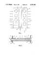
- a reactor tube 25(typically fabricated from quartz), houses a plurality of substrates 26 and is disposed within a cylindrical furnace 27 and heated therein to a temperature of from 300° C. to 450° C.
- An outlet port 28 of the reactor tube 25is typically connected to an evacuation pump, (not shown), for evacuating spent or exhausted vapors.
- a hydride manifold 29has vapor distributing openings 30 deposited therein, in the vicinity of the substrates, ensuring an even supply of vapors to the substrates and uniform deposition thereon.
- An oxygen manifold(not shown) is placed beside the hydride manifold in a well known manner.
- a pair of concentric tubes 31A and 31Benvelope the hydride manifold 29, and have apertures therein coterminous with the vapor distributing openings 30.
- a loading door assembly 35is provided for inserting and removing substrates 26 and is maintained in sealed relation to the reactor tube 25 via a well known seal such as "O" rings 36. Also, a vacuum tight seal 37 seals the pair of concentric tubes 31A and B to the quartz reactor tube 25.
- the hydride vapor mixtureenters the manifold 29 at contact 32 and is expelled through openings 30.
- the hydride vapor mixturereacts with the oxygen at the surfaces of the substrates 26, forming a coating thereon as discussed above..
- the spent vaporsare expelled through outlet port 28 in response to operation of the evacuation pump. Cooling fluid flows through the concentric tubes 31A and 31B entering at port 33 and flowing out contact 34, thereby cooling the boron hydride vapor (B 2 H 6 ) to a temperature less than at least 200° C.
- the ratio of the inner surface area of reactor tube 25 to the surface area of the manifold arrangementwas approximately 100.
- the diameter of the reactor tube 25was approximately 10 times that of the manifold arrangement.
- Prior art manifoldswere typically fabricated from transparent material such as quartz. It has been found that infrared photons are typically transmitted through the prior art manifolds and absorbed by the reactive vapors. In response, the vapors typically become energized to above the thermal energy level within the manifolds, thereby accelerating chemical vapor deposition and causing premature reaction of the vapors. It has been found that fabricating the manifold arrangement with a photon reflecting material (such as stainless steel), or using a cooling fluid having the ability to absorb the photons, significantly reduces deposition inside the manifold. For practical purposes water has been found to exhibit adequate photon absorbing characteristics.
- the inventionis not restricted to use with those compounds, and numerous other films or coatings can be advantageously deposited according to the present invention.
- the inventioncan be used to apply doped polysilicon coatings, wear and corrosion resistant boron film coatings, or aluminum coatings reacted from triisobutilaluminum to one or more substrates.
- intermetallic semiconductorsgallium arsenide, gallium phosphide, etc.
- metalorganic compounds[Ga(CH 3 ) 3 , Al(C 2 H 5 ) 3 , etc.] and deposited on the substrates.
Landscapes
- Chemical & Material Sciences (AREA)
- General Chemical & Material Sciences (AREA)
- Chemical Kinetics & Catalysis (AREA)
- Engineering & Computer Science (AREA)
- Materials Engineering (AREA)
- Mechanical Engineering (AREA)
- Metallurgy (AREA)
- Organic Chemistry (AREA)
- Chemical Vapour Deposition (AREA)
- Formation Of Insulating Films (AREA)
Abstract
Description
Claims (14)
Applications Claiming Priority (2)
| Application Number | Priority Date | Filing Date | Title |
|---|---|---|---|
| CA000481854ACA1251100A (en) | 1985-05-17 | 1985-05-17 | Chemical vapor deposition |
| CA481854 | 1985-05-17 |
Related Parent Applications (1)
| Application Number | Title | Priority Date | Filing Date |
|---|---|---|---|
| US06778238Continuation | 1985-09-20 |
Publications (1)
| Publication Number | Publication Date |
|---|---|
| US4747368Atrue US4747368A (en) | 1988-05-31 |
Family
ID=4130515
Family Applications (1)
| Application Number | Title | Priority Date | Filing Date |
|---|---|---|---|
| US07/035,032Expired - LifetimeUS4747368A (en) | 1985-05-17 | 1987-04-06 | Chemical vapor deposition apparatus with manifold enveloped by cooling means |
Country Status (8)
| Country | Link |
|---|---|
| US (1) | US4747368A (en) |
| JP (2) | JPS6258639A (en) |
| CN (1) | CN85109048A (en) |
| CA (1) | CA1251100A (en) |
| DE (1) | DE3601711A1 (en) |
| FR (1) | FR2582021A1 (en) |
| GB (1) | GB2175011B (en) |
| IT (1) | IT1186780B (en) |
Cited By (38)
| Publication number | Priority date | Publication date | Assignee | Title |
|---|---|---|---|---|
| US4910042A (en)* | 1987-07-30 | 1990-03-20 | Jiri Hokynar | Apparatus and method for treating material surfaces |
| WO1990010092A1 (en)* | 1989-02-24 | 1990-09-07 | Massachusetts Institute Of Technology | A modified stagnation flow apparatus for chemical vapor deposition providing excellent control of the deposition |
| US4981103A (en)* | 1987-10-08 | 1991-01-01 | Anelva Corporation | Apparatus for forming a metal thin film utilizing temperature controlling means |
| US4997677A (en)* | 1987-08-31 | 1991-03-05 | Massachusetts Institute Of Technology | Vapor phase reactor for making multilayer structures |
| US5000113A (en)* | 1986-12-19 | 1991-03-19 | Applied Materials, Inc. | Thermal CVD/PECVD reactor and use for thermal chemical vapor deposition of silicon dioxide and in-situ multi-step planarized process |
| US5129360A (en)* | 1990-01-24 | 1992-07-14 | The United States Of America As Represented By The Secretary Of The Air Force | Actively cooled effusion cell for chemical vapor deposition |
| US5261963A (en)* | 1991-12-04 | 1993-11-16 | Howmet Corporation | CVD apparatus comprising exhaust gas condensation means |
| US5264245A (en)* | 1991-12-04 | 1993-11-23 | Howmet Corporation | CVD method for forming uniform coatings |
| US5431769A (en)* | 1992-10-31 | 1995-07-11 | Sony Corporation | Method and system for plasma treatment |
| US5461214A (en)* | 1992-06-15 | 1995-10-24 | Thermtec, Inc. | High performance horizontal diffusion furnace system |
| US5755886A (en)* | 1986-12-19 | 1998-05-26 | Applied Materials, Inc. | Apparatus for preventing deposition gases from contacting a selected region of a substrate during deposition processing |
| US5773100A (en)* | 1987-08-14 | 1998-06-30 | Applied Materials, Inc | PECVD of silicon nitride films |
| US5904567A (en)* | 1984-11-26 | 1999-05-18 | Semiconductor Energy Laboratory Co., Ltd. | Layer member forming method |
| US6100105A (en)* | 1996-05-10 | 2000-08-08 | Sumitomo Chemical Company, Ltd. | Fabrication of InGaAlN based compound semiconductor device |
| US6204197B1 (en) | 1984-02-15 | 2001-03-20 | Semiconductor Energy Laboratory Co., Ltd. | Semiconductor device, manufacturing method, and system |
| US6221164B1 (en) | 2000-01-25 | 2001-04-24 | Advanced Micro Devices, Inc. | Method of in-situ cleaning for LPCVD teos pump |
| US6230650B1 (en) | 1985-10-14 | 2001-05-15 | Semiconductor Energy Laboratory Co., Ltd. | Microwave enhanced CVD system under magnetic field |
| US6564810B1 (en) | 2000-03-28 | 2003-05-20 | Asm America | Cleaning of semiconductor processing chambers |
| US6666924B1 (en) | 2000-03-28 | 2003-12-23 | Asm America | Reaction chamber with decreased wall deposition |
| US6673722B1 (en) | 1985-10-14 | 2004-01-06 | Semiconductor Energy Laboratory Co., Ltd. | Microwave enhanced CVD system under magnetic field |
| US20040025786A1 (en)* | 2002-04-05 | 2004-02-12 | Tadashi Kontani | Substrate processing apparatus and reaction container |
| US6769908B2 (en)* | 2001-02-13 | 2004-08-03 | Semiconductor Leading Edge Technologies, Inc. | Wafer heat-treatment system and wafer heat-treatment method |
| US6784033B1 (en) | 1984-02-15 | 2004-08-31 | Semiconductor Energy Laboratory Co., Ltd. | Method for the manufacture of an insulated gate field effect semiconductor device |
| US6786997B1 (en) | 1984-11-26 | 2004-09-07 | Semiconductor Energy Laboratory Co., Ltd. | Plasma processing apparatus |
| US6793966B2 (en) | 2001-09-10 | 2004-09-21 | Howmet Research Corporation | Chemical vapor deposition apparatus and method |
| US6902623B2 (en) | 2001-06-07 | 2005-06-07 | Veeco Instruments Inc. | Reactor having a movable shutter |
| US20080286980A1 (en)* | 2005-03-01 | 2008-11-20 | Hitachi Kokusai Electric Inc. | Substrate Processing Apparatus and Semiconductor Device Producing Method |
| US20080292430A1 (en)* | 2007-05-21 | 2008-11-27 | Centrotherm Photovoltaics Ag | Device for doping, deposition or oxidation of semiconductor material at low pressure |
| US20090074984A1 (en)* | 2007-09-19 | 2009-03-19 | Hitachi Kokusai Electric, Inc. | Substrate processing apparatus and coating method |
| US20090071403A1 (en)* | 2007-09-19 | 2009-03-19 | Soo Young Choi | Pecvd process chamber with cooled backing plate |
| US20090071406A1 (en)* | 2007-09-19 | 2009-03-19 | Soo Young Choi | Cooled backing plate |
| US20090151632A1 (en)* | 2006-03-28 | 2009-06-18 | Hitachi Kokusai Electric Inc. | Substrate Processing Apparatus |
| US20120279943A1 (en)* | 2011-05-03 | 2012-11-08 | Applied Materials, Inc. | Processing chamber with cooled gas delivery line |
| US20140144380A1 (en)* | 2012-11-28 | 2014-05-29 | Samsung Electronics Co., Ltd. | Gas supply pipes and chemical vapor deposition apparatus |
| JP2015521381A (en)* | 2012-05-25 | 2015-07-27 | ククチェ エレクトリック コリア カンパニー リミテッド | Nozzle unit and substrate processing equipment having the nozzle unit |
| US10364498B2 (en)* | 2014-03-31 | 2019-07-30 | Kabushiki Kaisha Toshiba | Gas supply pipe, and gas treatment equipment |
| US20210108313A1 (en)* | 2019-10-14 | 2021-04-15 | Samsung Electronics Co., Ltd. | Semiconductor manufacturing apparatus |
| US11248295B2 (en) | 2014-01-27 | 2022-02-15 | Veeco Instruments Inc. | Wafer carrier having retention pockets with compound radii for chemical vapor deposition systems |
Families Citing this family (4)
| Publication number | Priority date | Publication date | Assignee | Title |
|---|---|---|---|---|
| JPS6313323A (en)* | 1986-07-04 | 1988-01-20 | Hitachi Ltd | Manufacture of thin film and device therefor |
| JP2839720B2 (en)* | 1990-12-19 | 1998-12-16 | 株式会社東芝 | Heat treatment equipment |
| FR2674618B1 (en)* | 1991-03-27 | 1998-03-13 | Etudes Const Mecaniques | NITRURATION PROCESS AND OVEN. |
| TW202426696A (en)* | 2022-11-18 | 2024-07-01 | 荷蘭商Asm Ip私人控股有限公司 | Gas injector and semiconductor processing apparatus including the same |
Citations (13)
| Publication number | Priority date | Publication date | Assignee | Title |
|---|---|---|---|---|
| US2700365A (en)* | 1951-10-08 | 1955-01-25 | Ohio Commw Eng Co | Apparatus for plating surfaces with carbonyls and other volatile metal bearing compounds |
| US2909148A (en)* | 1956-09-13 | 1959-10-20 | Nat Res Corp | Coating |
| US3098763A (en)* | 1961-05-29 | 1963-07-23 | Raytheon Co | Chemical reactor |
| US3481781A (en)* | 1967-03-17 | 1969-12-02 | Rca Corp | Silicate glass coating of semiconductor devices |
| US3818982A (en)* | 1971-10-27 | 1974-06-25 | Balzers Patent Beteilig Ag | Device for cooling workpieces which are submitted to a vacuum treatment |
| US3862397A (en)* | 1972-03-24 | 1975-01-21 | Applied Materials Tech | Cool wall radiantly heated reactor |
| US4030964A (en)* | 1976-04-29 | 1977-06-21 | The United States Of America As Represented By The United States Energy Research And Development Administration | Temperature cycling vapor deposition HgI2 crystal growth |
| US4047496A (en)* | 1974-05-31 | 1977-09-13 | Applied Materials, Inc. | Epitaxial radiation heated reactor |
| US4167915A (en)* | 1977-03-09 | 1979-09-18 | Atomel Corporation | High-pressure, high-temperature gaseous chemical apparatus |
| US4315479A (en)* | 1980-06-27 | 1982-02-16 | Atomel Corporation | Silicon wafer steam oxidizing apparatus |
| US4545327A (en)* | 1982-08-27 | 1985-10-08 | Anicon, Inc. | Chemical vapor deposition apparatus |
| US4557950A (en)* | 1984-05-18 | 1985-12-10 | Thermco Systems, Inc. | Process for deposition of borophosphosilicate glass |
| US4565157A (en)* | 1983-03-29 | 1986-01-21 | Genus, Inc. | Method and apparatus for deposition of tungsten silicides |
Family Cites Families (5)
| Publication number | Priority date | Publication date | Assignee | Title |
|---|---|---|---|---|
| DE2626446C3 (en)* | 1976-06-12 | 1978-12-14 | Hobeg Hochtemperaturreaktor-Brennelement Gmbh, 6450 Hanau | Process for the coating of particles for the production of fuel and / or absorber elements for nuclear reactors and apparatus therefor |
| JPS5524424A (en)* | 1978-08-09 | 1980-02-21 | Kokusai Electric Co Ltd | Forming device of pressure-reduced epitaxial layer |
| JPS6016757B2 (en)* | 1978-10-11 | 1985-04-27 | 株式会社東芝 | semiconductor equipment |
| JPS5618415A (en)* | 1979-07-24 | 1981-02-21 | Sanyo Electric Co Ltd | Apparatus for epitaxial growth |
| JPS6168393A (en)* | 1984-09-11 | 1986-04-08 | Touyoko Kagaku Kk | Hot wall type epitaxial growth device |
- 1985
- 1985-05-17CACA000481854Apatent/CA1251100A/ennot_activeExpired
- 1985-10-18ITIT22537/85Apatent/IT1186780B/enactive
- 1985-10-18GBGB08525789Apatent/GB2175011B/ennot_activeExpired
- 1985-11-12CNCN198585109048Apatent/CN85109048A/enactivePending
- 1986
- 1986-01-22DEDE19863601711patent/DE3601711A1/enactiveGranted
- 1986-04-11FRFR8605324Apatent/FR2582021A1/ennot_activeWithdrawn
- 1986-05-15JPJP61112420Apatent/JPS6258639A/enactivePending
- 1987
- 1987-04-06USUS07/035,032patent/US4747368A/ennot_activeExpired - Lifetime
- 1994
- 1994-07-11JPJP008270Upatent/JPH0728963U/enactivePending
Patent Citations (13)
| Publication number | Priority date | Publication date | Assignee | Title |
|---|---|---|---|---|
| US2700365A (en)* | 1951-10-08 | 1955-01-25 | Ohio Commw Eng Co | Apparatus for plating surfaces with carbonyls and other volatile metal bearing compounds |
| US2909148A (en)* | 1956-09-13 | 1959-10-20 | Nat Res Corp | Coating |
| US3098763A (en)* | 1961-05-29 | 1963-07-23 | Raytheon Co | Chemical reactor |
| US3481781A (en)* | 1967-03-17 | 1969-12-02 | Rca Corp | Silicate glass coating of semiconductor devices |
| US3818982A (en)* | 1971-10-27 | 1974-06-25 | Balzers Patent Beteilig Ag | Device for cooling workpieces which are submitted to a vacuum treatment |
| US3862397A (en)* | 1972-03-24 | 1975-01-21 | Applied Materials Tech | Cool wall radiantly heated reactor |
| US4047496A (en)* | 1974-05-31 | 1977-09-13 | Applied Materials, Inc. | Epitaxial radiation heated reactor |
| US4030964A (en)* | 1976-04-29 | 1977-06-21 | The United States Of America As Represented By The United States Energy Research And Development Administration | Temperature cycling vapor deposition HgI2 crystal growth |
| US4167915A (en)* | 1977-03-09 | 1979-09-18 | Atomel Corporation | High-pressure, high-temperature gaseous chemical apparatus |
| US4315479A (en)* | 1980-06-27 | 1982-02-16 | Atomel Corporation | Silicon wafer steam oxidizing apparatus |
| US4545327A (en)* | 1982-08-27 | 1985-10-08 | Anicon, Inc. | Chemical vapor deposition apparatus |
| US4565157A (en)* | 1983-03-29 | 1986-01-21 | Genus, Inc. | Method and apparatus for deposition of tungsten silicides |
| US4557950A (en)* | 1984-05-18 | 1985-12-10 | Thermco Systems, Inc. | Process for deposition of borophosphosilicate glass |
Cited By (64)
| Publication number | Priority date | Publication date | Assignee | Title |
|---|---|---|---|---|
| US6204197B1 (en) | 1984-02-15 | 2001-03-20 | Semiconductor Energy Laboratory Co., Ltd. | Semiconductor device, manufacturing method, and system |
| US6784033B1 (en) | 1984-02-15 | 2004-08-31 | Semiconductor Energy Laboratory Co., Ltd. | Method for the manufacture of an insulated gate field effect semiconductor device |
| US6984595B1 (en) | 1984-11-26 | 2006-01-10 | Semiconductor Energy Laboratory Co., Ltd. | Layer member forming method |
| US6786997B1 (en) | 1984-11-26 | 2004-09-07 | Semiconductor Energy Laboratory Co., Ltd. | Plasma processing apparatus |
| US5904567A (en)* | 1984-11-26 | 1999-05-18 | Semiconductor Energy Laboratory Co., Ltd. | Layer member forming method |
| US6230650B1 (en) | 1985-10-14 | 2001-05-15 | Semiconductor Energy Laboratory Co., Ltd. | Microwave enhanced CVD system under magnetic field |
| US6673722B1 (en) | 1985-10-14 | 2004-01-06 | Semiconductor Energy Laboratory Co., Ltd. | Microwave enhanced CVD system under magnetic field |
| US5755886A (en)* | 1986-12-19 | 1998-05-26 | Applied Materials, Inc. | Apparatus for preventing deposition gases from contacting a selected region of a substrate during deposition processing |
| US5362526A (en)* | 1986-12-19 | 1994-11-08 | Applied Materials, Inc. | Plasma-enhanced CVD process using TEOS for depositing silicon oxide |
| US6167834B1 (en) | 1986-12-19 | 2001-01-02 | Applied Materials, Inc. | Thermal CVD/PECVD reactor and use for thermal chemical vapor deposition of silicon dioxide and in-situ multi-step planarized process |
| US5000113A (en)* | 1986-12-19 | 1991-03-19 | Applied Materials, Inc. | Thermal CVD/PECVD reactor and use for thermal chemical vapor deposition of silicon dioxide and in-situ multi-step planarized process |
| US5871811A (en)* | 1986-12-19 | 1999-02-16 | Applied Materials, Inc. | Method for protecting against deposition on a selected region of a substrate |
| US4910042A (en)* | 1987-07-30 | 1990-03-20 | Jiri Hokynar | Apparatus and method for treating material surfaces |
| US5773100A (en)* | 1987-08-14 | 1998-06-30 | Applied Materials, Inc | PECVD of silicon nitride films |
| US4997677A (en)* | 1987-08-31 | 1991-03-05 | Massachusetts Institute Of Technology | Vapor phase reactor for making multilayer structures |
| US4981103A (en)* | 1987-10-08 | 1991-01-01 | Anelva Corporation | Apparatus for forming a metal thin film utilizing temperature controlling means |
| WO1990010092A1 (en)* | 1989-02-24 | 1990-09-07 | Massachusetts Institute Of Technology | A modified stagnation flow apparatus for chemical vapor deposition providing excellent control of the deposition |
| US5129360A (en)* | 1990-01-24 | 1992-07-14 | The United States Of America As Represented By The Secretary Of The Air Force | Actively cooled effusion cell for chemical vapor deposition |
| US5261963A (en)* | 1991-12-04 | 1993-11-16 | Howmet Corporation | CVD apparatus comprising exhaust gas condensation means |
| US5264245A (en)* | 1991-12-04 | 1993-11-23 | Howmet Corporation | CVD method for forming uniform coatings |
| US5462013A (en)* | 1991-12-04 | 1995-10-31 | Howmet Corporation | CVD apparatus and method for forming uniform coatings |
| US5407704A (en)* | 1991-12-04 | 1995-04-18 | Howmet Corporation | CVD apparatus and method |
| US5461214A (en)* | 1992-06-15 | 1995-10-24 | Thermtec, Inc. | High performance horizontal diffusion furnace system |
| US5517001A (en)* | 1992-06-15 | 1996-05-14 | Thermtec, Inc. | High performance horizontal diffusion furnace system |
| US5483041A (en)* | 1992-06-15 | 1996-01-09 | Thermtec, Inc. | Thermocouple for a horizontal diffusion furnace |
| US5530222A (en)* | 1992-06-15 | 1996-06-25 | Thermtec, Inc. | Apparatus for positioning a furnace module in a horizontal diffusion furnace |
| US5431769A (en)* | 1992-10-31 | 1995-07-11 | Sony Corporation | Method and system for plasma treatment |
| US6100105A (en)* | 1996-05-10 | 2000-08-08 | Sumitomo Chemical Company, Ltd. | Fabrication of InGaAlN based compound semiconductor device |
| US6221164B1 (en) | 2000-01-25 | 2001-04-24 | Advanced Micro Devices, Inc. | Method of in-situ cleaning for LPCVD teos pump |
| US6498104B1 (en) | 2000-01-25 | 2002-12-24 | Advanced Micro Devices, Inc. | Method of in-situ cleaning for LPCVD TEOS pump |
| US6564810B1 (en) | 2000-03-28 | 2003-05-20 | Asm America | Cleaning of semiconductor processing chambers |
| US6666924B1 (en) | 2000-03-28 | 2003-12-23 | Asm America | Reaction chamber with decreased wall deposition |
| US6708700B2 (en) | 2000-03-28 | 2004-03-23 | Asm America | Cleaning of semiconductor processing chambers |
| US6769908B2 (en)* | 2001-02-13 | 2004-08-03 | Semiconductor Leading Edge Technologies, Inc. | Wafer heat-treatment system and wafer heat-treatment method |
| US20050217578A1 (en)* | 2001-06-07 | 2005-10-06 | Alexander Gurary | Reactor having a movable shutter |
| US7276124B2 (en) | 2001-06-07 | 2007-10-02 | Veeco Instruments Inc. | Reactor having a movable shutter |
| US6902623B2 (en) | 2001-06-07 | 2005-06-07 | Veeco Instruments Inc. | Reactor having a movable shutter |
| US6911234B2 (en) | 2001-09-10 | 2005-06-28 | Howmet Corporation | Chemical vapor deposition apparatus and method |
| US6793966B2 (en) | 2001-09-10 | 2004-09-21 | Howmet Research Corporation | Chemical vapor deposition apparatus and method |
| US20050000439A1 (en)* | 2001-09-10 | 2005-01-06 | Howmet Research Corporation | Chemical vapor deposition apparatus and method |
| US20080251015A1 (en)* | 2002-04-05 | 2008-10-16 | Tadashi Kontani | Substrate Processing Apparatus and Reaction Container |
| US20080121180A1 (en)* | 2002-04-05 | 2008-05-29 | Tadashi Kontani | Substrate Processing Apparatus and Reaction Container |
| US20080251014A1 (en)* | 2002-04-05 | 2008-10-16 | Tadashi Kontani | Substrate Processing Apparatus and Reaction Container |
| US8261692B2 (en) | 2002-04-05 | 2012-09-11 | Hitachi Kokusai Electric Inc. | Substrate processing apparatus and reaction container |
| US20040025786A1 (en)* | 2002-04-05 | 2004-02-12 | Tadashi Kontani | Substrate processing apparatus and reaction container |
| US7900580B2 (en)* | 2002-04-05 | 2011-03-08 | Hitachi Kokusai Electric Inc. | Substrate processing apparatus and reaction container |
| US8047158B2 (en)* | 2002-04-05 | 2011-11-01 | Hitachi Kokusai Electric Inc. | Substrate processing apparatus and reaction container |
| US20080286980A1 (en)* | 2005-03-01 | 2008-11-20 | Hitachi Kokusai Electric Inc. | Substrate Processing Apparatus and Semiconductor Device Producing Method |
| US8251012B2 (en)* | 2005-03-01 | 2012-08-28 | Hitachi Kokusai Electric Inc. | Substrate processing apparatus and semiconductor device producing method |
| US8176871B2 (en)* | 2006-03-28 | 2012-05-15 | Hitachi Kokusai Electric Inc. | Substrate processing apparatus |
| US20090151632A1 (en)* | 2006-03-28 | 2009-06-18 | Hitachi Kokusai Electric Inc. | Substrate Processing Apparatus |
| US20080292430A1 (en)* | 2007-05-21 | 2008-11-27 | Centrotherm Photovoltaics Ag | Device for doping, deposition or oxidation of semiconductor material at low pressure |
| US8460468B2 (en) | 2007-05-21 | 2013-06-11 | Centrotherm Photovoltaics Ag | Device for doping, deposition or oxidation of semiconductor material at low pressure |
| WO2009039343A1 (en)* | 2007-09-19 | 2009-03-26 | Applied Materials, Inc. | Pecvd process chamber with cooled backing plate |
| US20090071406A1 (en)* | 2007-09-19 | 2009-03-19 | Soo Young Choi | Cooled backing plate |
| US20090071403A1 (en)* | 2007-09-19 | 2009-03-19 | Soo Young Choi | Pecvd process chamber with cooled backing plate |
| US20090074984A1 (en)* | 2007-09-19 | 2009-03-19 | Hitachi Kokusai Electric, Inc. | Substrate processing apparatus and coating method |
| US20120279943A1 (en)* | 2011-05-03 | 2012-11-08 | Applied Materials, Inc. | Processing chamber with cooled gas delivery line |
| JP2015521381A (en)* | 2012-05-25 | 2015-07-27 | ククチェ エレクトリック コリア カンパニー リミテッド | Nozzle unit and substrate processing equipment having the nozzle unit |
| US20140144380A1 (en)* | 2012-11-28 | 2014-05-29 | Samsung Electronics Co., Ltd. | Gas supply pipes and chemical vapor deposition apparatus |
| US11248295B2 (en) | 2014-01-27 | 2022-02-15 | Veeco Instruments Inc. | Wafer carrier having retention pockets with compound radii for chemical vapor deposition systems |
| US10364498B2 (en)* | 2014-03-31 | 2019-07-30 | Kabushiki Kaisha Toshiba | Gas supply pipe, and gas treatment equipment |
| US20210108313A1 (en)* | 2019-10-14 | 2021-04-15 | Samsung Electronics Co., Ltd. | Semiconductor manufacturing apparatus |
| US11913114B2 (en)* | 2019-10-14 | 2024-02-27 | Samsung Electronics Co., Ltd. | Semiconductor manufacturing apparatus |
Also Published As
| Publication number | Publication date |
|---|---|
| JPS6258639A (en) | 1987-03-14 |
| GB2175011B (en) | 1989-01-11 |
| GB8525789D0 (en) | 1985-11-20 |
| DE3601711C2 (en) | 1987-09-10 |
| FR2582021A1 (en) | 1986-11-21 |
| IT8522537A0 (en) | 1985-10-18 |
| GB2175011A (en) | 1986-11-19 |
| CN85109048A (en) | 1986-11-05 |
| JPH0728963U (en) | 1995-05-30 |
| IT1186780B (en) | 1987-12-16 |
| CA1251100A (en) | 1989-03-14 |
| DE3601711A1 (en) | 1986-11-20 |
Similar Documents
| Publication | Publication Date | Title |
|---|---|---|
| US4747368A (en) | Chemical vapor deposition apparatus with manifold enveloped by cooling means | |
| US4232063A (en) | Chemical vapor deposition reactor and process | |
| US4098923A (en) | Pyrolytic deposition of silicon dioxide on semiconductors using a shrouded boat | |
| US5871586A (en) | Chemical vapor deposition | |
| US4699805A (en) | Process and apparatus for the low pressure chemical vapor deposition of thin films | |
| US4592933A (en) | High efficiency homogeneous chemical vapor deposition | |
| US4545327A (en) | Chemical vapor deposition apparatus | |
| US3916822A (en) | Chemical vapor deposition reactor | |
| US5525157A (en) | Gas injectors for reaction chambers in CVD systems | |
| US4653428A (en) | Selective chemical vapor deposition apparatus | |
| EP0464515A2 (en) | Method of manufacturing silicon nitride film | |
| US5116784A (en) | Method of forming semiconductor film | |
| US5225378A (en) | Method of forming a phosphorus doped silicon film | |
| GB2089840A (en) | Chemical vapour deposition apparatus incorporating radiant heat source for substrate | |
| US5264038A (en) | Chemical vapor deposition system | |
| JP3551609B2 (en) | Heat treatment equipment | |
| US4547404A (en) | Chemical vapor deposition process | |
| US20010000160A1 (en) | Method for treatment of semiconductor substrates | |
| US5180692A (en) | Method for the manufacture of boron-containing films by CVD or epitaxial techniques using boron trifluoride | |
| US20010018894A1 (en) | Vertical low-pressure chemical vapor deposition furnace | |
| US3658032A (en) | Reactor for the formation of material on a substrate | |
| EP0223787A1 (en) | Selective chemical vapor deposition method and apparatus. | |
| JPH04243122A (en) | chemical vapor deposition equipment | |
| JPS6251919B2 (en) | ||
| JP2581093Y2 (en) | Semiconductor heat treatment equipment |
Legal Events
| Date | Code | Title | Description |
|---|---|---|---|
| STCF | Information on status: patent grant | Free format text:PATENTED CASE | |
| FPAY | Fee payment | Year of fee payment:4 | |
| FEPP | Fee payment procedure | Free format text:PAYOR NUMBER ASSIGNED (ORIGINAL EVENT CODE: ASPN); ENTITY STATUS OF PATENT OWNER: LARGE ENTITY | |
| FPAY | Fee payment | Year of fee payment:8 | |
| AS | Assignment | Owner name:CANADIAN IMPERIAL BANK OF COMMERCE, AS SECURED PAR Free format text:GRANT OF PATENT SECURITY INTEREST;ASSIGNOR:MITEL CORPORATION, A CORP. OF CANADA;REEL/FRAME:009114/0489 Effective date:19980212 | |
| FPAY | Fee payment | Year of fee payment:12 | |
| AS | Assignment | Owner name:MITEL CORPORATION, CANADA Free format text:RELEASE BY SECURED PARTY;ASSIGNOR:CANADIAN IMPERIAL BANK OF COMMERCE;REEL/FRAME:011590/0406 Effective date:20010216 Owner name:MITEL, INC., A DELAWARE CORPORATION, CANADA Free format text:RELEASE BY SECURED PARTY;ASSIGNOR:CANADIAN IMPERIAL BANK OF COMMERCE;REEL/FRAME:011590/0406 Effective date:20010216 Owner name:MITEL SEMICONDUCTOR, INC., A DELAWARE CORPORATION, Free format text:RELEASE BY SECURED PARTY;ASSIGNOR:CANADIAN IMPERIAL BANK OF COMMERCE;REEL/FRAME:011590/0406 Effective date:20010216 Owner name:MITEL SEMICONDUCTOR, LIMITED, CANADA Free format text:RELEASE BY SECURED PARTY;ASSIGNOR:CANADIAN IMPERIAL BANK OF COMMERCE;REEL/FRAME:011590/0406 Effective date:20010216 Owner name:MITEL TELCOM LIMITED CORPORATION, CANADA Free format text:RELEASE BY SECURED PARTY;ASSIGNOR:CANADIAN IMPERIAL BANK OF COMMERCE;REEL/FRAME:011590/0406 Effective date:20010216 Owner name:MITEL SEMICONDUCTOR AMERICAS, INC., A DELAWARE COR Free format text:RELEASE BY SECURED PARTY;ASSIGNOR:CANADIAN IMPERIAL BANK OF COMMERCE;REEL/FRAME:011590/0406 Effective date:20010216 | |
| AS | Assignment | Owner name:ZARLINK SEMICONDUCTOR INC., CANADA Free format text:CHANGE OF NAME;ASSIGNORS:MITEL CORPORATON;MITEL S.C.C.;REEL/FRAME:012590/0484 Effective date:20010725 |