US4742551A - Multistatistics gatherer - Google Patents
Multistatistics gathererDownload PDFInfo
- Publication number
- US4742551A US4742551AUS06/785,352US78535285AUS4742551AUS 4742551 AUS4742551 AUS 4742551AUS 78535285 AUS78535285 AUS 78535285AUS 4742551 AUS4742551 AUS 4742551A
- Authority
- US
- United States
- Prior art keywords
- input
- signal
- select
- address
- value
- Prior art date
- Legal status (The legal status is an assumption and is not a legal conclusion. Google has not performed a legal analysis and makes no representation as to the accuracy of the status listed.)
- Expired - Fee Related
Links
Images


Classifications
- G—PHYSICS
- G06—COMPUTING OR CALCULATING; COUNTING
- G06F—ELECTRIC DIGITAL DATA PROCESSING
- G06F17/00—Digital computing or data processing equipment or methods, specially adapted for specific functions
- G06F17/10—Complex mathematical operations
- G06F17/18—Complex mathematical operations for evaluating statistical data, e.g. average values, frequency distributions, probability functions, regression analysis
- G—PHYSICS
- G06—COMPUTING OR CALCULATING; COUNTING
- G06T—IMAGE DATA PROCESSING OR GENERATION, IN GENERAL
- G06T7/00—Image analysis
- G06T7/60—Analysis of geometric attributes
- G06T7/62—Analysis of geometric attributes of area, perimeter, diameter or volume
- G—PHYSICS
- G06—COMPUTING OR CALCULATING; COUNTING
- G06V—IMAGE OR VIDEO RECOGNITION OR UNDERSTANDING
- G06V10/00—Arrangements for image or video recognition or understanding
- G06V10/40—Extraction of image or video features
- G06V10/50—Extraction of image or video features by performing operations within image blocks; by using histograms, e.g. histogram of oriented gradients [HoG]; by summing image-intensity values; Projection analysis
- G06V10/507—Summing image-intensity values; Histogram projection analysis
Definitions
- the inventionrelates generally to digital image processing and, more particularly, to the statistical analysis of digital images for use in processing the image and for determining characteristics of objects in the image.
- Recent advances in automationutilize artificial intelligence to identify objects and to provide information relating to the position, shape, orientation, and other characteristics of the objects.
- the "eye" of the artificial intelligence systemis a video camera and processor that generates a digital images or frames.
- Each frameis comprised of pixels which are digital values assigned to unit areas of an image or frame.
- the pixel output from a video camerais a gray scale value indicating light intensity at a specified unit area.
- the location of a pixel in the frameis indicated by its x,y coordinates.
- the y coordinateidentifies the line of the frame and the x coordinate identifies the position in the line of the pixel.
- the "brain” of the systemmust interpret the image.
- One method of interpreting the imageis to store in memory some selected characteristics of a reference object.
- the video systemthen analyzes the video image to determine the selected characteristics of objects in the image. These determined characteristics of the objects in the image may then be compared to the stored characteristics of the reference object.
- the imagePrior to determination of object characteristics the image is converted from a gray scale to a binary image. This conversion includes statistical analysis of the image to determine a suitable threshold level. Pixels having a gray scale value above the threshold are converted to binary ones and pixels having a gray scale value below the threshold are converted to binary zeros.
- the selected characteristics of the imaged objectsare determined by statistical connectivity analysis of a binary image.
- the processingis performed in several stages. First, the image is subjected to connectivity analysis for identifying connected regions in the image. Each separate region is given a unique label where the labeled regions correspond to major objects in the image. Statistics pertaining to the number of pixels in a region, the positions of pixels in the region, and the number of pixels on the boundary of a region are then computed for each object separately. These statistics are utilized to determine characteristics of an object, its area (size), its centroid (center), its major axis (orientation), and its length-to-width ratio (squat? thin?). These characteristics are then used as the basis for further processing.
- the x and y projections of an objectmay be compared to equivalent statistics for a referenced object.
- an entire frameis stored in memory and the various algorithms are utilized to perform statistical measurements on the objects in the frame.
- a video cameragenerates 30 to 60 frames per second with each frame comprising over up to 250,000 or more pixels.
- These existing systemsutilize computers to perform the statistical measurements described above. Typically these measurements take many multiples of the 1/30 sec. frame time to complete for each frame.
- the calculated statisticsare utilized by the system processor to determine object characteristics for use in image interpretation.
- the results of the image interpretationmay be utilized to control an automated system.
- the speed of image interpretationis critical to increase the efficiency of the automated system.
- the image interpretation processis slow relative to the video rate of operation of the camera or "eye" of the system.
- These existing systemsare not able to provide the statistical measurements to the system processor at the end of each frame. For example, although 30 to 60 frames could be supplied every second, it can take over a second to analyze the results of a single frame. Thus, the "brain" of the system is much slower than the "eye.”
- the present inventionis a multifunctional unit for use in the connectivity analysis subsystem of a video image processing system.
- the multifunctional unitcomputes statistics relating to the number and positions of pixels in a region of a video image.
- the multifunctional unitmay also be utilized to compute the x and y projection of a region in either a gray scale or binary image and to generate histograms of pixels in an image.
- the results of the statistical analyses and computationsare generated at the video rate at which frames are provided to the system.
- the subsystemincludes a register bank for gathering statistics.
- the register bankis configured as a random access memory (RAM) having an address input port for accepting an address-select signal.
- the address-select signalselects a particular register.
- the RAMalso includes a write enable input (WE), a data input port, and a data output port.
- WEwrite enable input
- An ALUhas a first ALU input port coupled to the RAM data output port, a seocnd ALU input port for receiving an increment value, and an ALU output port coupled to the data input port of the RAM. During an increment cycle, the ALU increments the word stored in a register specified by the address-select signal by the increment value.
- the subsystemincludes a first pixel input for receiving a pixel in a frame and a function generator for generating a function output signal specifying the value of an arithmetic function of the x and y coordinates of the received pixel.
- the received pixel and the function output signalmay be utilized as either the address-select or increment value.
- the subsystemincludes a second pixel input.
- Either pixel inputcan be coupled to either the address input port of the RAM or the second input of the adder.
- a constant registeris included in the subsystem.
- An address multiplexercouples the address input port to either the first pixel input, the second pixel input, the function generator, or the constant register.
- an increment multiplexercouples the second input of the adder to either the first pixel input, the second pixel input, the function generator, or the constant register.
- two or more subsystemsmay operate in parallel with a single address space defined.
- a comparatorreceives the high order bits of the address signal at one input and the contents of a TAG register at its other input. The output of the comparator is coupled to the WE port.
- a selected word stored in an addressed registermay be divided into max and min segments.
- the ALUis configured to determine whether an input value at the second ALU input port is greater than the max value encoded by the max field or less than a min value encoded by the min field. If the input value is greater than the max value, then the max segment is modified to encode the input value. If the input value is less than the min value, then the min segment is modified to encode the input value. If the input value is between the max and min values, then neither the max nor min segments are modified. Subsequent to the compare and modify operations, the selected word is written into the addressed register. In this mode, the multifunctional unit can compute the boundary rectangle of a connected region in an image.
- the subsystemis fabricated on a single silicon IC chip utilizing VLSI technology.
- the IC chipincludes a microprocessor interface for coupling the chip to a system processor.
- the processorprovides control signals to the chip through an interface. Additionally, data is transferred between the chip and the processor via the interface.
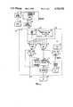
- FIG. 1is a block diagram of an embodiment of the invention
- FIG. 2is a block diagram of a thresholding system utilizing the present invention
- FIG. 3is a block diagram of a system for performing connectivity analysis utilizing the present invention
- FIG. 4a diagram of a connectivity analyzed region
- FIG. 5is a block diagram of a system for measuring the perimeter of a region utilizing the present invention.
- FIG. 5Ais a block diagram of a system having an address space defined over two parallel MSG chips
- FIG. 6Ais a schematic diagram of a register bank
- FIG. 6Bis a diagram of an image illustrating the x projection of an object
- FIG. 7is a schematic diagram of the register bank illustrating the computation of an x projection
- FIG. 8is a diagram of the output of a morphology chip
- FIG. 9is a graph of a gray scale histogram
- FIG. 10is a block diagram of the function generator.
- FIG. 1is a schematic diagram of a preferred embodiment of the invention.
- the systemis fabricated on a single IC multistatistics gatherer (MSG) chip 10 utilizing standard VLSI technology.
- a high speed random access memory (RAM) 12has an address input port 14, a data input port 16, a data output port 18, a write enable (WE) input 19, and an interface port 20.
- the RAM 12is a bank of 256 32-bit registers.
- An ALU 26has a first ALU input 27 coupled to the data output port 18 of the RAM, and a second ALU input 28.
- An increment select MUX 34has a select signal output port 36 coupled to the second ALU input port 28 of the ALU 26.
- the increment multiplexer 34also includes a set of increment select input ports 38.
- An address select multiplexer 44has an address select output port 46 coupled to the address input port 14 of the RAM 12.
- the address select multiplexerhas four address select input ports 48.
- a first pixel input external port 54is coupled to the first address select input port of the address select MUX 44 and the first increment select port of the increment select MUX 34.
- a constant register 56has an output port coupled to the second address select input port 48 of the address select multiplexer 44 and to the second increment select input port 38 of the increment select multiplexer 34.
- a function generator 66has a handshake signal input port 67 coupled to handshake signal external port 67e.
- the function generator 66may be configured to generate a selected f(x,y) of the x and y coordinates of a pixel.
- the output port 68 of the function generator 66is coupled to the third address select input port 48 of the address select multiplexer 44 and to the third increment select port 38 of the increment select multiplexer 34.
- a second pixel input external port 70is coupled to the fourth address select input port 48 of the address select multiplexer 44 and to the fourth increment select input port 38 of the increment select multiplexer 34.
- a comparator 72has a first comparator input 76 coupled to the address select output port 46 of the address select multiplexer 44, and a second comparator input 78.
- a tab register 80includes an output port coupled to the second comparator input 78 of the comparator 72. The output of the comparator 72 is coupled to the WE input 19 of the RAM 12.
- a clock signal external pin 86supplies a clock signal to synchronize the operations of the system components.
- a microprocessor interface 87couples the IC MSG chip 10 to a system processor 88.
- the interface port 20 of the RAM 12is coupled to the processor interface 87.
- a control unit 89is coupled to the processor interface 87.
- the control unit 89controls the increment and address-select MUXs 34 and 44, selects the function to be generated by the function generator 66, loads the constant and TAB registers 56 and 80 and performs other control functions through the interface 87.
- the connections between the control unit 89 and functional elements on the MSG chip 10are standard and not shown.
- Datais transferred between the RAM 12 and the processor 88 via the interface 87.
- FIG. 1elements of the image processing system external to the MSG chip 10 are depicted in FIG. 1 to facilitate describing the operation of the invention.
- the screen 90 of the video camera in the systemis divided into elementary units of area 92.
- the level of analog output signalindicates the image intensity on a given unit area.
- This signalis digitized by an ADC 93 to form a digitized gray scale pixel.
- the entire screenin scanned by an image scan control system 94 to form an image or frame.
- the framesare generated at a video rate determined by the frame clock 96.
- the pixel processing rateis about 10 to 20 MHz.
- the pixelsare routed to an image processing system 98.
- the frame clock 96generates a pixel processing clock signal at the pixel processing rate.
- the scan control circuitry 94includes a handshake output coupled to the handshake input external port of the chip 67e. First and second handshake signals are asserted at the end of each line scan and at the beginning of each frame, respectively.
- FIG. 2is a block diagram of an image processing system in which the MSG chip 10 is utilized to form a histogram of gray scale values for use in the thresholding system that converts a gray scale image to a binary image.
- a camera and synch generator 100has its output coupled to the input of an ADC 93.
- the output of the ADC 93is coupled to the first pixel input 54 of the MSG chip 10 and to the input port of a dual-ported frame buffer 102.
- the output of the frame buffer 102is coupled to a look-up table (LUT) 104.
- a system processor 88is coupled, via processor interface circuitry, to the MSG chip 10, the frame buffer 102, and the LUT 104.
- the MSG chip 10is configured by the processor to form a histogram of the gray scale values of the pixels in one frame.
- the figureshows an exemplary histogram eight-level gray scale.
- the horizontal axisis divided into eight bins 108 with each bin for counting the number of pixels having one of the 8 possible gray scale value.
- the frame buffer 102is a large memory bank which stores the incoming pixels until all the pixels of frame have arrived.
- the processor 88reads the histogram at the end of each frame, and applies a standard algorithm to determine a threshold value.
- the threshold valueis used to create a thresholding function to be loaded into the LUT 104.
- the image pixelsare transferred from the frame buffer 102 to the thresholded LUT 104.
- the output image from the LUT 104is a binary image having pixels with values of binary zero or binary one only.
- FIG. 3is a schematic diagram of a system utilizing the MSG chip 10 to measure statistics of a region in an image.
- the camera 100is coupled to the ADC 93.
- the ADC outputis received by an image filtering conditioning subsystem 200.
- the output of the subsystem 200is transferred to a thresholding system 202, e.g., a system as depicted in FIG. 2.
- the output of the thresholding subsystem 202is coupled to the input of a connectivity analysis chip 204.
- the output of the connectivity analysis chip 204is coupled to the first pixel inputs 54 of a set of MSG chips 10.
- the MSG chips 10are coupled to a microprocessor 88 via the microprocessor interface 87 of each MSG chip 10.
- the function of the connectivity chip 204will be briefly described with reference to FIG. 4.
- a frame 92 depicted in FIG. 4includes first, second, and third connected regions 300, 302, and 304.
- the connectivity chipassigns a selected numeric label to each pixel in a connected region. For example, every pixel in the first region 300 is assigned the value 1, every pixel in the second region 302 is assigned the value 2, and every pixel in the third region 304 is assigned the value 3.
- the processor 88configures the control unit 89 on each MSG chip 10 to cause the chip to measure a particular statistic related to the regions in a frame.
- a first chipmay be configured to compute the sum of the x coordinate of each pixel for each region ( ⁇ x).
- Other statistical quantities that may be computedinclude ⁇ y, ⁇ x 2 , ⁇ y 2 , and ⁇ xy.
- the area of each regionmay be computed by counting the number of pixels in the region, ( ⁇ 1).
- an MSG chip 10to compute an external feature, i.e., the perimeter, of a connected region in a frame will now be described with reference to FIG. 5.
- the output of the thresholding subsystem 202is coupled to the inputs of a connectivity analysis chip 204 and of a morphology chip 300.
- the output of the connectivity analysis chip 204is coupled to the first pixel input of an MSG chip 10.
- the output of the morphology chip 300is coupled to the second input of the MSG chip 10.
- the morphology chip 300may be configured to assign a value of one to a pixel on the perimeter of a connected region and a value of zero to all other pixels in the frame.
- the MSG chip 10is configured by the processor 88 to count the number of pixels in the perimeter of each region.
- one of the MSG chips 10may be configured by the processor to compute the projection of a single object in a frame on either the vertical, y, axis or the horizontal, x, axis of the frame.
- Each MSG chip 10may compute only a single projection of one object in the frame. Accordingly, with the addition of look-up tables, several chips may be connected in parallel to compute the projections of a number of objects in a single frame.
- FIG. 4the boundary rectangle 305 of the third connected region 304 is depicted.
- This boundary rectangle 305is defined by the values x min , X max , Y min , and Y max , which are computed by the MSG chip 10.
- the clock input 56must be coupled to a clock synchronized at the rate at which pixels are supplied to the pixel inputs 54 and 70.
- the clock input 56is coupled to the clock controlling the pixel output rate of the ADC 93.
- a typical image processing problemis the following.
- a system processoris programmed to discard all objects having an area less than A(ref), or to discard all objects with centroids positioned between x 1 (Ref) and x 2 (Ref).
- the statistical computations required to determine these characteristics of each regionare the number of pixels in the region, the sum of the x coordinates of all the pixels in a given region ( ⁇ x), the sum of the y coordinates of all the pixels in a given region ( ⁇ y). Additionally, the statistical quantities ⁇ x 2 , ⁇ y 2 , and ⁇ xy may be utilized to determine the elongation and orientation of the region.
- the configuration of the MSG chip 10 to perform the functions describedare listed in Table 1.
- the first column inputindicates whether the pixel value indicates the intensity of the pixel, i.e. gray scale, or indicates the connected regions in a binary image frame, i.e. labelled binary.
- the second column, address-selindicates the input signal to the address input 14 of the RAM 12
- the third column, increment-selindicates the signal at the second input port 28 of the ALU 26, and the final column, statistic computed, indicates the information contained in the statistical measurement or the object characteristic which may be determined from the statistic computed.
- FIG. 6Ais a schematic diagram of the RAM 12 showing the storage location of the RAM as registers or bins 400. The statistical computation of the area of a region will be described with reference to FIGS. 1, 4, and 6.
- the increment select multiplexer 34is set to couple the output of the constant register 56 to the second input of the adder 26.
- the constant in the constant register 56is set to 1.
- the address select multiplexer 46is set to couple the first pixel input pin 54 to the address input port 14 of the RAM 12.
- the pixel input valuesare either 0, 1, 2, or 3.
- the pixel input valuesare either 0, 1, 2, or 3.
- the value of each pixeldetermines which storage bin is accessed. For example, for each pixel in the third region 304, the word in bin 3 is accessed and directed to the adder 26. The value of the accessed word is incremented by the constant (equal 1) in the constant register and returned to bin 3.
- the number stored in bin 3is equal to the number of pixels in the third region 304. This number is a measure of the area of bin 3 since each pixel represents a unit area of the image frame.
- the numbers stored in bins 1 and 2are measures of the area of regions 1 and 2.
- an MSG chip 10provides the area of first, second and third regions 300, 302, 304 to the processor 88.
- the increment select multiplexer 34is controlled to couple the output port 68 of the function generator 66 to the second input port 28 of the adder 26.
- the address select multiplexer 46is controlled to couple the first pixel input pin 54 to the address input port 14 of the RAM 12.
- the value of the pixeldetermines which storage bin is accessed. For example, each pixel in the third region 304, the word in bin 3 is accessed and directed to the adder 26. The value of the word is incremented by the value of the x coordinate of the pixel and returned to bin 3. Thus, when the frame scan is completed, the number stored in bin 3 is equal to the sum of the x values of each pixel in the third region 304.
- the processorcalculates the x coordinate centroid of the third region 304 by dividing this sum by the area of the third region 304 supplied from another MSG chip 10 in the set depicted in FIG. 3.
- FIGS. 6A, 6B, and 7.An image is defined in the frame 92.
- the projection of the region on the x axisis another feature of interest of an object of the region.
- the address select MUX 44is controlled to couple the output port 68 of the function generator 66 to the address input port 14 of the RAM 12.
- the increment select multiplexer 34is controlled to couple the first pixel input pin 54 to the second input of the adder 26.
- the x coordinate of each pixel inputaccesses the bin 130 having an address equal to x.
- the ALU 26can be configured to simultaneously perform a max/min comparison between an input value and max and min values encoded in max and min segments of a word stored in an addressed register.
- the first sixteen bits of a 32 bit selected word in the addressed registercould be the min segment encoding a min value and the second sixteen bits could be a max segment encoding a max value.
- the selected wordis directed to the first input 27 of the ALU 26.
- the min and max valuesare compared to an input value at the second input of the ALU 26. If the input value is less than the min value, then min segment of the selected word is modified to encode the input value and the max segment is unmodified. If the input value is greater than the max value, then the max field is modified to encode the input value and the min field is unmodified. If the input value is between the min and max values then neither the min segment nor the max segment is modified.
- the selected wordis directed back to the addressed register upon completion of the comparison and modification operations.
- the x min /x max determinationis performed utilizing a labelled binary image as depicted in FIG. 4.
- the first pixel input port 58is coupled to address port 14 of the RAM 12.
- each pixel in the third regionis labelled with the numeral 3.
- the x value of the pixelis compared to the min and max values stored in the third register.
- the min segmentis modified if the x value is less than the min value or the max segment is modified if the x value is greater than the max value.
- the min valuewill be the smallest x value of any pixel in the third region 304, i.e., x min .
- the max valuewill be the greatest x value of any pixel in the third region 304, i.e., x max .
- FIG. 5Adepicts a configuration having 2 MSG chips 10 configured to define a signal address space having 512 registers in the RAM 12.
- the first inputs of MSG chips 10A and 10Bare coupled to the output port of the connectivity chip 204.
- FIGS. 6B and 7An example of the need for an extended address space is an x-projection computation as illustrated in FIGS. 6B and 7.
- the registers in the RAM 12are addressed by the x coordinate of the object 500. If the image width is greater than 255, then a single MSG chip 10 would run out of registers.
- a single address spacemay be defined utilizing the TAG register 80 and comparator 27 (FIG. 1).
- the MSG chip 10Aincludes registers 0 to 255 and MSG chip 10B includes registers 256 to 511.
- the ninth bit of the nine or more bit binary address for registers 0 to 255is equal to zero and for registers 256 to 511 is equal to one.
- the ninth bit of the address-select signal from the address MUX 44is directed to the first comparator input 76 of MSG chips 10A and 10B.
- chip 10Athe content of the TAG register 80 is set to zero and in chip 10B the content of the TAG register 80 is set to one.
- the ninth bitis zero and the output of the comparator 27 in MSG chip 10A is high and in chip 10B is low. Thus, only the WE input 19 of the RAM 12 in chip 10A is enabled. The pixel value is written into a register of the RAM 12 in chip 10A.
- the ninth bitis one and output of the comparator 27 in chip 10A is low and in chip 10B is high. Thus, only the WE input of the RAM 12 in chip 10B is enabled. The pixel value is written into a register of the RAM 12 in chip 10B. Thus, an extended address space is defined that allows an operation to be stacked over more than one chip.
- the output of the morphology chip 300is depicted. Pixels on the perimeter of the region are assigned the value of one and all other pixels in the region are assigned the value zero.
- the output of the connectivity chip 204is connected to the first pixel input 54 of the MSG chip 10 and the output of the morphology chip 300 is connected to the second pixel input 70.
- the increment MUX 34is controlled to couple the second pixel input 70 to the second input of the adder 26.
- the address MUX 44is controlled to couple the first pixel input 54 to the address input port 14.
- a pixel in the backgroundis assigned the value zero by both the connectivity chip 204 and the morphology chip 300.
- the zeroth binis addressed by the connectivity chip output and the word in the zeroth bin is incremented by zero.
- the zero binis not incremented for pixels in the background area.
- the bin having address number 1is selected by the output from the connectivity chip and the word in bin 1 is incremented by zero, the value of the pixel from the morphology chip.
- the bin 1is selected by the output of the connectivity chip and the word stored in bin 1 is incremented by one, the value of the pixel from the morphology chip.
- the value in bin 1is incremented by the number of pixels on the perimeter of the region during one frame scan. This number is a measure of the perimeter and is computed for each object.
- a gray scale histogramtypically the gray scale is divided into 256 intervals, with the zeroth interval being black and the 255th interval representing the highest light intensity.
- the histogramindicates the number of pixels in a frame having each value in the gray scale.
- the first pixel input 70is coupled to the address input port 14 by the address MUX 44.
- the value in the constant register 56is set to one and the output of the constant register is coupled to the second input of the adder 26 by the increment multiplexer 34.
- each pixeladdresses a bin representing the gray scale value of the pixel.
- the word in the binis incremented by one each time a pixel having that gray scale is inputted.
- a gray scale histogramhas been constructed. This operation can be stacked for longer histogramming.
- an accumulator 600has a handshake input 602 coupled to handshake port 67.
- a counter 604has a handshake input coupled to handshake pin 67.
- An adder 606has a left input coupled to the output of the counter 604 and an output coupled to the input of the counter 604.
- the output of the counter 604is also coupled to a first input of a MUX 608.
- the second input of the MUX 608is coupled to the output of a constant register 610.
- the right input of a second adder 612is coupled to the output of MUX 608 and a right input of the second adder 612 is coupled to the output port of the accumulator 600.
- the output port of the second adder 612is coupled to the input port of the accumulator 600.
- the output port of the accumulator 600is coupled to the output port 68 of the function generator 66.
- the first handshake signalis asserted and at the end of each line in a frame the second handshake signal is asserted.
- These handshake signalsare received at port 67.
- the accumulator 600 and counter 604 valuesare set by the control logic 89 at the beginning of each frame and end of each line according to the function to be calculated. Additionally, the accumulator 600 and counter 604 values are incremented by the control logic 89 (FIG. 1) upon the receipt of each new pixel.
- Table 2depicts the accumulator (ACC) and counter (CTR) values for each new frame, each new pixel received during a frame, and at the end of each line in a frame for the functions x, y, xy, x 2 , and y 2 .
- ACCaccumulator
- CTRcounter
- x 2 , xy, and y 2utilizes an iterative technique. For example, once an x 2 i value has been determined for a given pixel i then the x 2 i+1 value for the next pixel is given by:
- the value of x 2 i+1is determined by knowledge of x 2 i and x i .
- the first and second pixel input portsare, in fact, general data input ports.
- the first general data input portcould be coupled to a microprocessor to receive the instructions generated by the microprocessor while executing a program. If the first data input port is coupled to the address port of the RAM and the ALU is configured to increment by one, a histogram of the occurrences of instructions while executing the program will be generated. The histogram will be complete when the program is complete.
Landscapes
- Engineering & Computer Science (AREA)
- Physics & Mathematics (AREA)
- General Physics & Mathematics (AREA)
- Theoretical Computer Science (AREA)
- Data Mining & Analysis (AREA)
- Mathematical Analysis (AREA)
- Mathematical Physics (AREA)
- Pure & Applied Mathematics (AREA)
- Mathematical Optimization (AREA)
- Computational Mathematics (AREA)
- Bioinformatics & Cheminformatics (AREA)
- Multimedia (AREA)
- Bioinformatics & Computational Biology (AREA)
- Operations Research (AREA)
- Probability & Statistics with Applications (AREA)
- Life Sciences & Earth Sciences (AREA)
- Algebra (AREA)
- Evolutionary Biology (AREA)
- Databases & Information Systems (AREA)
- Software Systems (AREA)
- General Engineering & Computer Science (AREA)
- Geometry (AREA)
- Computer Vision & Pattern Recognition (AREA)
- Image Analysis (AREA)
Abstract
Description
TABLE 1 ______________________________________ Input Address-sel Increment-sel Statistic Computed ______________________________________gray scale input 1 constant = 1 histogram labelledinput 1 constant = 1 region areas binary labelled input 1 x first moment binary about x axis labelled input 1 y first moment binary about y axis labelledinput 1 x.sup.2 second moment binary about x axis labelledinput 1 y.sup.2 second moment binary about y axis labelledinput 1 xy summed xy binary labelledinput 1input 2 count external binary feature gray scale,x input 1 x-projection binary, or labelled binary gray scale, y input 1 y-projection binary, or labelled binary labelled input 1 x x.sub.min, x.sub.max binary labelled input 1 y y.sub.min, y.sub.max binary ______________________________________
TABLE 2 __________________________________________________________________________Function New Frame New Pixel End Line __________________________________________________________________________x ACC ← 0 ACC ← ACC + 1 ACC ← 0 y ACC ← 0 ACC ← ACC + 1 xy ACC ← 0 ACC ← ACC + CTR ACC ← 0 CTR ← 0 CTR ← CTR + 1 x.sup.2 ACC ← 0 ACC ← ACC + CTR + 1 ACC ← 0 CTR ← 0 CTR ← CTR + 2 CTR ← 0 y.sup.2 ACC ← 0 ACC ← ACC + CTR + 1 CTR ← 0 CTR ← CTR + 2 __________________________________________________________________________
x.sup.2.sub.i+1 =(x.sub.i +1).sup.2 =x.sub.i.sup.2 +2x.sub.i +1EQUATION 1
ACC.sub.1 =ACC.sub.0 (=0)+CTR.sub.0 (=0)+1=1=x.sup.2.sub.1EQUATION 2
CTR.sub.1 =CTR.sub.0 (=0)+2=2EQUATION 3
ACC.sub.2 =ACC.sub.1 (=1)+CTR.sub.1 (=2)+1=4=x.sup.2.sub.2EQUATION 4
CTR.sub.2 =CTR.sub.1 (=2)+2=4 EQUATION 5
Claims (11)
Priority Applications (1)
| Application Number | Priority Date | Filing Date | Title |
|---|---|---|---|
| US06/785,352US4742551A (en) | 1985-10-07 | 1985-10-07 | Multistatistics gatherer |
Applications Claiming Priority (1)
| Application Number | Priority Date | Filing Date | Title |
|---|---|---|---|
| US06/785,352US4742551A (en) | 1985-10-07 | 1985-10-07 | Multistatistics gatherer |
Publications (1)
| Publication Number | Publication Date |
|---|---|
| US4742551Atrue US4742551A (en) | 1988-05-03 |
Family
ID=25135223
Family Applications (1)
| Application Number | Title | Priority Date | Filing Date |
|---|---|---|---|
| US06/785,352Expired - Fee RelatedUS4742551A (en) | 1985-10-07 | 1985-10-07 | Multistatistics gatherer |
Country Status (1)
| Country | Link |
|---|---|
| US (1) | US4742551A (en) |
Cited By (49)
| Publication number | Priority date | Publication date | Assignee | Title |
|---|---|---|---|---|
| FR2633747A1 (en)* | 1988-07-01 | 1990-01-05 | Telecommunications Sa | Adaptive image-processing system |
| US4953227A (en)* | 1986-01-31 | 1990-08-28 | Canon Kabushiki Kaisha | Image mosaic-processing method and apparatus |
| US4972359A (en)* | 1987-04-03 | 1990-11-20 | Cognex Corporation | Digital image processing system |
| EP0398314A3 (en)* | 1989-05-16 | 1991-08-07 | Matsushita Electric Industrial Co., Ltd. | An apparatus for binarizing image signals |
| US5040226A (en)* | 1988-05-31 | 1991-08-13 | Trw Financial Systems, Inc. | Courtesy amount read and transaction balancing system |
| US5065444A (en)* | 1988-02-08 | 1991-11-12 | Northrop Corporation | Streak removal filtering method and apparatus |
| US5077808A (en)* | 1988-05-16 | 1991-12-31 | Ezel Inc. | Method for processing an image by histogram alteration |
| US5280544A (en)* | 1987-07-24 | 1994-01-18 | Sharp Kabushiki Kaisha | Optical character reading apparatus and method |
| US5335293A (en)* | 1992-06-16 | 1994-08-02 | Key Technology, Inc. | Product inspection method and apparatus |
| US5583954A (en)* | 1994-03-01 | 1996-12-10 | Cognex Corporation | Methods and apparatus for fast correlation |
| US5872870A (en)* | 1996-02-16 | 1999-02-16 | Cognex Corporation | Machine vision methods for identifying extrema of objects in rotated reference frames |
| US5887079A (en)* | 1996-01-31 | 1999-03-23 | Sumitomo Metal Industries Limited | Image processing apparatus |
| US5909504A (en)* | 1996-03-15 | 1999-06-01 | Cognex Corporation | Method of testing a machine vision inspection system |
| US5953130A (en)* | 1997-01-06 | 1999-09-14 | Cognex Corporation | Machine vision methods and apparatus for machine vision illumination of an object |
| US5960125A (en)* | 1996-11-21 | 1999-09-28 | Cognex Corporation | Nonfeedback-based machine vision method for determining a calibration relationship between a camera and a moveable object |
| US5974169A (en)* | 1997-03-20 | 1999-10-26 | Cognex Corporation | Machine vision methods for determining characteristics of an object using boundary points and bounding regions |
| US5978080A (en)* | 1997-09-25 | 1999-11-02 | Cognex Corporation | Machine vision methods using feedback to determine an orientation, pixel width and pixel height of a field of view |
| US5978502A (en)* | 1996-04-01 | 1999-11-02 | Cognex Corporation | Machine vision methods for determining characteristics of three-dimensional objects |
| US6023522A (en)* | 1997-05-05 | 2000-02-08 | Draganoff; Georgi H. | Inexpensive adaptive fingerprint image acquisition framegrabber |
| US6025854A (en)* | 1997-12-31 | 2000-02-15 | Cognex Corporation | Method and apparatus for high speed image acquisition |
| US6026176A (en)* | 1995-07-25 | 2000-02-15 | Cognex Corporation | Machine vision methods and articles of manufacture for ball grid array inspection |
| US6067379A (en)* | 1988-12-09 | 2000-05-23 | Cognex Corporation | Method and apparatus for locating patterns in an optical image |
| US6075876A (en)* | 1997-05-07 | 2000-06-13 | Draganoff; Georgi Hristoff | Sliding yardsticks fingerprint enrollment and verification system and method |
| US6075881A (en)* | 1997-03-18 | 2000-06-13 | Cognex Corporation | Machine vision methods for identifying collinear sets of points from an image |
| US6108446A (en)* | 1997-02-18 | 2000-08-22 | Hoshen; Joseph | Method and apparatus for extracting cluster shape features from digital images |
| US6137893A (en)* | 1996-10-07 | 2000-10-24 | Cognex Corporation | Machine vision calibration targets and methods of determining their location and orientation in an image |
| US6141033A (en)* | 1997-05-15 | 2000-10-31 | Cognex Corporation | Bandwidth reduction of multichannel images for machine vision |
| US6215915B1 (en) | 1998-02-20 | 2001-04-10 | Cognex Corporation | Image processing methods and apparatus for separable, general affine transformation of an image |
| US6236769B1 (en) | 1998-01-28 | 2001-05-22 | Cognex Corporation | Machine vision systems and methods for morphological transformation of an image with zero or other uniform offsets |
| US6259827B1 (en) | 1996-03-21 | 2001-07-10 | Cognex Corporation | Machine vision methods for enhancing the contrast between an object and its background using multiple on-axis images |
| US6282328B1 (en) | 1998-01-28 | 2001-08-28 | Cognex Corporation | Machine vision systems and methods for morphological transformation of an image with non-uniform offsets |
| US6298149B1 (en) | 1996-03-21 | 2001-10-02 | Cognex Corporation | Semiconductor device image inspection with contrast enhancement |
| US6381366B1 (en) | 1998-12-18 | 2002-04-30 | Cognex Corporation | Machine vision methods and system for boundary point-based comparison of patterns and images |
| US6381375B1 (en) | 1998-02-20 | 2002-04-30 | Cognex Corporation | Methods and apparatus for generating a projection of an image |
| US20030068086A1 (en)* | 2001-10-05 | 2003-04-10 | International Business Machines Corporation | Image processing method, system, computer program and data carrier |
| US6608647B1 (en) | 1997-06-24 | 2003-08-19 | Cognex Corporation | Methods and apparatus for charge coupled device image acquisition with independent integration and readout |
| US6684402B1 (en) | 1999-12-01 | 2004-01-27 | Cognex Technology And Investment Corporation | Control methods and apparatus for coupling multiple image acquisition devices to a digital data processor |
| US6687402B1 (en) | 1998-12-18 | 2004-02-03 | Cognex Corporation | Machine vision methods and systems for boundary feature comparison of patterns and images |
| US6748104B1 (en) | 2000-03-24 | 2004-06-08 | Cognex Corporation | Methods and apparatus for machine vision inspection using single and multiple templates or patterns |
| US6845176B1 (en) | 1998-03-17 | 2005-01-18 | Sharp Laboratories Of America, Inc. | System and method for on-line computation and storage of scene histograms in an image acquisition appliance |
| US20050038942A1 (en)* | 1999-08-17 | 2005-02-17 | Eric Swanson | Data converter with statistical domain output |
| US7006669B1 (en) | 2000-12-31 | 2006-02-28 | Cognex Corporation | Machine vision method and apparatus for thresholding images of non-uniform materials |
| US20070116352A1 (en)* | 2001-11-13 | 2007-05-24 | Cyberoptics Corporation | Pick and place machine with component placement inspection |
| EP1152372A3 (en)* | 2000-05-01 | 2008-04-02 | GE Medical Systems Global Technology Company LLC | Method and apparatus for automatic detection and sizing of cystic objects |
| US7639861B2 (en) | 2005-09-14 | 2009-12-29 | Cognex Technology And Investment Corporation | Method and apparatus for backlighting a wafer during alignment |
| US20100260417A1 (en)* | 2009-04-13 | 2010-10-14 | Canon Kabushiki Kaisha | Image processing apparatus and control method |
| US8111904B2 (en) | 2005-10-07 | 2012-02-07 | Cognex Technology And Investment Corp. | Methods and apparatus for practical 3D vision system |
| US8162584B2 (en) | 2006-08-23 | 2012-04-24 | Cognex Corporation | Method and apparatus for semiconductor wafer alignment |
| US9165209B2 (en)* | 2012-07-24 | 2015-10-20 | Samsung Electronics Co., Ltd. | Apparatus and method for calculating cumulative histogram of image |
Citations (7)
| Publication number | Priority date | Publication date | Assignee | Title |
|---|---|---|---|---|
| US3983320A (en)* | 1975-08-25 | 1976-09-28 | Hughes Aircraft Company | Raster display histogram equalization |
| US4212072A (en)* | 1978-03-07 | 1980-07-08 | Hughes Aircraft Company | Digital scan converter with programmable transfer function |
| US4365304A (en)* | 1979-08-27 | 1982-12-21 | Yeda Research & Development Co., Ltd. | Method and apparatus for on-line data enhancement |
| US4450482A (en)* | 1981-03-02 | 1984-05-22 | Siemens Aktiengesellschaft | Digital real-time video image processing device |
| US4606065A (en)* | 1984-02-09 | 1986-08-12 | Imaging Technology Incorporated | Image processing-system |
| US4624013A (en)* | 1984-03-31 | 1986-11-18 | Kabushiki Kaisha Toshiba | Linked component extraction circuit for image processor |
| US4672220A (en)* | 1984-09-04 | 1987-06-09 | Messerschmitt-Bolkow-Blohm Gmbh | Method and apparatus for reading out an opto-electric detector |
- 1985
- 1985-10-07USUS06/785,352patent/US4742551A/ennot_activeExpired - Fee Related
Patent Citations (7)
| Publication number | Priority date | Publication date | Assignee | Title |
|---|---|---|---|---|
| US3983320A (en)* | 1975-08-25 | 1976-09-28 | Hughes Aircraft Company | Raster display histogram equalization |
| US4212072A (en)* | 1978-03-07 | 1980-07-08 | Hughes Aircraft Company | Digital scan converter with programmable transfer function |
| US4365304A (en)* | 1979-08-27 | 1982-12-21 | Yeda Research & Development Co., Ltd. | Method and apparatus for on-line data enhancement |
| US4450482A (en)* | 1981-03-02 | 1984-05-22 | Siemens Aktiengesellschaft | Digital real-time video image processing device |
| US4606065A (en)* | 1984-02-09 | 1986-08-12 | Imaging Technology Incorporated | Image processing-system |
| US4624013A (en)* | 1984-03-31 | 1986-11-18 | Kabushiki Kaisha Toshiba | Linked component extraction circuit for image processor |
| US4672220A (en)* | 1984-09-04 | 1987-06-09 | Messerschmitt-Bolkow-Blohm Gmbh | Method and apparatus for reading out an opto-electric detector |
Cited By (59)
| Publication number | Priority date | Publication date | Assignee | Title |
|---|---|---|---|---|
| US4953227A (en)* | 1986-01-31 | 1990-08-28 | Canon Kabushiki Kaisha | Image mosaic-processing method and apparatus |
| US4972359A (en)* | 1987-04-03 | 1990-11-20 | Cognex Corporation | Digital image processing system |
| US5280544A (en)* | 1987-07-24 | 1994-01-18 | Sharp Kabushiki Kaisha | Optical character reading apparatus and method |
| US5065444A (en)* | 1988-02-08 | 1991-11-12 | Northrop Corporation | Streak removal filtering method and apparatus |
| US5077808A (en)* | 1988-05-16 | 1991-12-31 | Ezel Inc. | Method for processing an image by histogram alteration |
| US5040226A (en)* | 1988-05-31 | 1991-08-13 | Trw Financial Systems, Inc. | Courtesy amount read and transaction balancing system |
| US5193121A (en)* | 1988-05-31 | 1993-03-09 | Trw Financial Systems, Inc. | Courtesy amount read and transaction balancing system |
| FR2633747A1 (en)* | 1988-07-01 | 1990-01-05 | Telecommunications Sa | Adaptive image-processing system |
| US6067379A (en)* | 1988-12-09 | 2000-05-23 | Cognex Corporation | Method and apparatus for locating patterns in an optical image |
| EP0398314A3 (en)* | 1989-05-16 | 1991-08-07 | Matsushita Electric Industrial Co., Ltd. | An apparatus for binarizing image signals |
| US5166986A (en)* | 1989-05-16 | 1992-11-24 | Matsushita Electric Industrial Co., Ltd. | Apparatus for binarizing image signals |
| US5335293A (en)* | 1992-06-16 | 1994-08-02 | Key Technology, Inc. | Product inspection method and apparatus |
| US5583954A (en)* | 1994-03-01 | 1996-12-10 | Cognex Corporation | Methods and apparatus for fast correlation |
| US6026176A (en)* | 1995-07-25 | 2000-02-15 | Cognex Corporation | Machine vision methods and articles of manufacture for ball grid array inspection |
| US6442291B1 (en) | 1995-07-25 | 2002-08-27 | Cognex Corporation | Machine vision methods and articles of manufacture for ball grid array |
| US5887079A (en)* | 1996-01-31 | 1999-03-23 | Sumitomo Metal Industries Limited | Image processing apparatus |
| US5872870A (en)* | 1996-02-16 | 1999-02-16 | Cognex Corporation | Machine vision methods for identifying extrema of objects in rotated reference frames |
| US5909504A (en)* | 1996-03-15 | 1999-06-01 | Cognex Corporation | Method of testing a machine vision inspection system |
| US6396949B1 (en) | 1996-03-21 | 2002-05-28 | Cognex Corporation | Machine vision methods for image segmentation using multiple images |
| US6587582B1 (en) | 1996-03-21 | 2003-07-01 | Cognex Corporation | Semiconductor device image inspection with contrast enhancement |
| US6298149B1 (en) | 1996-03-21 | 2001-10-02 | Cognex Corporation | Semiconductor device image inspection with contrast enhancement |
| US6259827B1 (en) | 1996-03-21 | 2001-07-10 | Cognex Corporation | Machine vision methods for enhancing the contrast between an object and its background using multiple on-axis images |
| US5978502A (en)* | 1996-04-01 | 1999-11-02 | Cognex Corporation | Machine vision methods for determining characteristics of three-dimensional objects |
| US6137893A (en)* | 1996-10-07 | 2000-10-24 | Cognex Corporation | Machine vision calibration targets and methods of determining their location and orientation in an image |
| US5960125A (en)* | 1996-11-21 | 1999-09-28 | Cognex Corporation | Nonfeedback-based machine vision method for determining a calibration relationship between a camera and a moveable object |
| US6301396B1 (en) | 1996-11-21 | 2001-10-09 | Cognex Corporation | Nonfeedback-based machine vision methods for determining a calibration relationship between a camera and a moveable object |
| US5953130A (en)* | 1997-01-06 | 1999-09-14 | Cognex Corporation | Machine vision methods and apparatus for machine vision illumination of an object |
| US6108446A (en)* | 1997-02-18 | 2000-08-22 | Hoshen; Joseph | Method and apparatus for extracting cluster shape features from digital images |
| US6075881A (en)* | 1997-03-18 | 2000-06-13 | Cognex Corporation | Machine vision methods for identifying collinear sets of points from an image |
| US5974169A (en)* | 1997-03-20 | 1999-10-26 | Cognex Corporation | Machine vision methods for determining characteristics of an object using boundary points and bounding regions |
| US6023522A (en)* | 1997-05-05 | 2000-02-08 | Draganoff; Georgi H. | Inexpensive adaptive fingerprint image acquisition framegrabber |
| US6075876A (en)* | 1997-05-07 | 2000-06-13 | Draganoff; Georgi Hristoff | Sliding yardsticks fingerprint enrollment and verification system and method |
| US6301376B1 (en) | 1997-05-07 | 2001-10-09 | Georgi H. Draganoff | Segmented sliding yardsticks error tolerant fingerprint enrollment and verification system and method |
| US6141033A (en)* | 1997-05-15 | 2000-10-31 | Cognex Corporation | Bandwidth reduction of multichannel images for machine vision |
| US6608647B1 (en) | 1997-06-24 | 2003-08-19 | Cognex Corporation | Methods and apparatus for charge coupled device image acquisition with independent integration and readout |
| US5978080A (en)* | 1997-09-25 | 1999-11-02 | Cognex Corporation | Machine vision methods using feedback to determine an orientation, pixel width and pixel height of a field of view |
| US6025854A (en)* | 1997-12-31 | 2000-02-15 | Cognex Corporation | Method and apparatus for high speed image acquisition |
| US6236769B1 (en) | 1998-01-28 | 2001-05-22 | Cognex Corporation | Machine vision systems and methods for morphological transformation of an image with zero or other uniform offsets |
| US6282328B1 (en) | 1998-01-28 | 2001-08-28 | Cognex Corporation | Machine vision systems and methods for morphological transformation of an image with non-uniform offsets |
| US6381375B1 (en) | 1998-02-20 | 2002-04-30 | Cognex Corporation | Methods and apparatus for generating a projection of an image |
| US6215915B1 (en) | 1998-02-20 | 2001-04-10 | Cognex Corporation | Image processing methods and apparatus for separable, general affine transformation of an image |
| US6845176B1 (en) | 1998-03-17 | 2005-01-18 | Sharp Laboratories Of America, Inc. | System and method for on-line computation and storage of scene histograms in an image acquisition appliance |
| US6381366B1 (en) | 1998-12-18 | 2002-04-30 | Cognex Corporation | Machine vision methods and system for boundary point-based comparison of patterns and images |
| US6687402B1 (en) | 1998-12-18 | 2004-02-03 | Cognex Corporation | Machine vision methods and systems for boundary feature comparison of patterns and images |
| US6931513B2 (en)* | 1999-08-17 | 2005-08-16 | Eric Swanson | Data converter with statistical domain output |
| US20050038942A1 (en)* | 1999-08-17 | 2005-02-17 | Eric Swanson | Data converter with statistical domain output |
| US6684402B1 (en) | 1999-12-01 | 2004-01-27 | Cognex Technology And Investment Corporation | Control methods and apparatus for coupling multiple image acquisition devices to a digital data processor |
| US6748104B1 (en) | 2000-03-24 | 2004-06-08 | Cognex Corporation | Methods and apparatus for machine vision inspection using single and multiple templates or patterns |
| EP1152372A3 (en)* | 2000-05-01 | 2008-04-02 | GE Medical Systems Global Technology Company LLC | Method and apparatus for automatic detection and sizing of cystic objects |
| US7006669B1 (en) | 2000-12-31 | 2006-02-28 | Cognex Corporation | Machine vision method and apparatus for thresholding images of non-uniform materials |
| US7054486B2 (en)* | 2001-10-05 | 2006-05-30 | International Business Machines Corporation | Image processing method, system, computer program and data carrier |
| US20030068086A1 (en)* | 2001-10-05 | 2003-04-10 | International Business Machines Corporation | Image processing method, system, computer program and data carrier |
| US20070116352A1 (en)* | 2001-11-13 | 2007-05-24 | Cyberoptics Corporation | Pick and place machine with component placement inspection |
| US7639861B2 (en) | 2005-09-14 | 2009-12-29 | Cognex Technology And Investment Corporation | Method and apparatus for backlighting a wafer during alignment |
| US8111904B2 (en) | 2005-10-07 | 2012-02-07 | Cognex Technology And Investment Corp. | Methods and apparatus for practical 3D vision system |
| US8162584B2 (en) | 2006-08-23 | 2012-04-24 | Cognex Corporation | Method and apparatus for semiconductor wafer alignment |
| US20100260417A1 (en)* | 2009-04-13 | 2010-10-14 | Canon Kabushiki Kaisha | Image processing apparatus and control method |
| US8401306B2 (en)* | 2009-04-13 | 2013-03-19 | Canon Kabushiki Kaisha | Image processing apparatus and control method |
| US9165209B2 (en)* | 2012-07-24 | 2015-10-20 | Samsung Electronics Co., Ltd. | Apparatus and method for calculating cumulative histogram of image |
Similar Documents
| Publication | Publication Date | Title |
|---|---|---|
| US4742551A (en) | Multistatistics gatherer | |
| US4414685A (en) | Method and apparatus for pattern recognition and detection | |
| US4606065A (en) | Image processing-system | |
| US4742552A (en) | Vector image processing system | |
| US4464788A (en) | Dynamic data correction generator for an image analyzer system | |
| US4395698A (en) | Neighborhood transformation logic circuitry for an image analyzer system | |
| US4322716A (en) | Method and apparatus for pattern recognition and detection | |
| US4553260A (en) | Means and method of processing optical image edge data | |
| EP0628188A1 (en) | Method of identifying and characterizing a valid object by color | |
| JPH1166325A (en) | Object boundary determining method and apparatus, and recording medium storing object boundary determining program | |
| US4641356A (en) | Apparatus and method for implementing dilation and erosion transformations in grayscale image processing | |
| US5305398A (en) | Method and apparatus for scaling image data | |
| Weberruss et al. | ORB feature extraction and matching in hardware | |
| Duff | Parallel processors for digital image processing | |
| US4442543A (en) | Bit enable circuitry for an image analyzer system | |
| McCurry et al. | Xilinx FPGA implementation of an image classifier for object detection applications | |
| KR100424511B1 (en) | Semiconductor memory having computation function and processing device using the same | |
| US5887079A (en) | Image processing apparatus | |
| US5438682A (en) | Data processing system for rewriting parallel processor output data using a sequential processor | |
| US11682099B2 (en) | Hardware accelerator for integral image computation | |
| Johnston et al. | Optimisation of a colour segmentation and tracking algorithm for real-time FPGA implementation | |
| JP2003178312A (en) | Method and device for determining center of gravity of optical signal mark attached to moving object by photogrammetry | |
| US20090208104A1 (en) | Method for Single Pass Blob Image Analysis | |
| US8155450B2 (en) | Apparatus for single pass blob image analysis | |
| EP0447541B1 (en) | Image data processor system and method |
Legal Events
| Date | Code | Title | Description |
|---|---|---|---|
| AS | Assignment | Owner name:FAIRCHILD CAMERA & INSTRUMENT CORPORATION, 464 ELL Free format text:ASSIGNMENT OF ASSIGNORS INTEREST.;ASSIGNOR:DEERING, MICHAEL F.;REEL/FRAME:004574/0562 Effective date:19851004 | |
| AS | Assignment | Owner name:SCHLUMBERGER SYSTEMS AND SERVICES, INC., 1259 OAKM Free format text:ASSIGNMENT OF ASSIGNORS INTEREST.;ASSIGNOR:FAIRCHILD SEMICONDUCTOR CORPORATION;REEL/FRAME:004821/0860 Effective date:19871007 Owner name:SCHLUMBERGER SYSTEMS AND SERVICES, INC.,CALIFORNIA Free format text:ASSIGNMENT OF ASSIGNORS INTEREST;ASSIGNOR:FAIRCHILD SEMICONDUCTOR CORPORATION;REEL/FRAME:004821/0860 Effective date:19871007 | |
| FEPP | Fee payment procedure | Free format text:PAYOR NUMBER ASSIGNED (ORIGINAL EVENT CODE: ASPN); ENTITY STATUS OF PATENT OWNER: LARGE ENTITY | |
| FPAY | Fee payment | Year of fee payment:4 | |
| REMI | Maintenance fee reminder mailed | ||
| LAPS | Lapse for failure to pay maintenance fees | ||
| FP | Lapsed due to failure to pay maintenance fee | Effective date:19960508 | |
| AS | Assignment | Owner name:NATIONAL SEMICONDUCTOR CORPORATION, CALIFORNIA Free format text:ASSIGNMENT OF ASSIGNORS INTEREST;ASSIGNOR:FAIRCHILD SEMICONDUCTOR CORPORATION;REEL/FRAME:008059/0846 Effective date:19960726 | |
| FEPP | Fee payment procedure | Free format text:PAYER NUMBER DE-ASSIGNED (ORIGINAL EVENT CODE: RMPN); ENTITY STATUS OF PATENT OWNER: LARGE ENTITY Free format text:PAYOR NUMBER ASSIGNED (ORIGINAL EVENT CODE: ASPN); ENTITY STATUS OF PATENT OWNER: LARGE ENTITY | |
| STCH | Information on status: patent discontinuation | Free format text:PATENT EXPIRED DUE TO NONPAYMENT OF MAINTENANCE FEES UNDER 37 CFR 1.362 |