US4737208A - Method of fabricating multilayer structures with nonplanar surfaces - Google Patents
Method of fabricating multilayer structures with nonplanar surfacesDownload PDFInfo
- Publication number
- US4737208A US4737208AUS06/912,874US91287486AUS4737208AUS 4737208 AUS4737208 AUS 4737208AUS 91287486 AUS91287486 AUS 91287486AUS 4737208 AUS4737208 AUS 4737208A
- Authority
- US
- United States
- Prior art keywords
- layers
- cavity
- conformal
- adhesive
- release
- Prior art date
- Legal status (The legal status is an assumption and is not a legal conclusion. Google has not performed a legal analysis and makes no representation as to the accuracy of the status listed.)
- Expired - Fee Related
Links
Images


Classifications
- H—ELECTRICITY
- H05—ELECTRIC TECHNIQUES NOT OTHERWISE PROVIDED FOR
- H05K—PRINTED CIRCUITS; CASINGS OR CONSTRUCTIONAL DETAILS OF ELECTRIC APPARATUS; MANUFACTURE OF ASSEMBLAGES OF ELECTRICAL COMPONENTS
- H05K3/00—Apparatus or processes for manufacturing printed circuits
- H05K3/46—Manufacturing multilayer circuits
- H05K3/4697—Manufacturing multilayer circuits having cavities, e.g. for mounting components
- H—ELECTRICITY
- H01—ELECTRIC ELEMENTS
- H01L—SEMICONDUCTOR DEVICES NOT COVERED BY CLASS H10
- H01L21/00—Processes or apparatus adapted for the manufacture or treatment of semiconductor or solid state devices or of parts thereof
- H01L21/02—Manufacture or treatment of semiconductor devices or of parts thereof
- H01L21/04—Manufacture or treatment of semiconductor devices or of parts thereof the devices having potential barriers, e.g. a PN junction, depletion layer or carrier concentration layer
- H01L21/48—Manufacture or treatment of parts, e.g. containers, prior to assembly of the devices, using processes not provided for in a single one of the groups H01L21/18 - H01L21/326 or H10D48/04 - H10D48/07
- H01L21/4814—Conductive parts
- H01L21/4846—Leads on or in insulating or insulated substrates, e.g. metallisation
- H01L21/4857—Multilayer substrates
- H—ELECTRICITY
- H05—ELECTRIC TECHNIQUES NOT OTHERWISE PROVIDED FOR
- H05K—PRINTED CIRCUITS; CASINGS OR CONSTRUCTIONAL DETAILS OF ELECTRIC APPARATUS; MANUFACTURE OF ASSEMBLAGES OF ELECTRICAL COMPONENTS
- H05K1/00—Printed circuits
- H05K1/18—Printed circuits structurally associated with non-printed electric components
- H05K1/182—Printed circuits structurally associated with non-printed electric components associated with components mounted in the printed circuit board, e.g. insert mounted components [IMC]
- H—ELECTRICITY
- H05—ELECTRIC TECHNIQUES NOT OTHERWISE PROVIDED FOR
- H05K—PRINTED CIRCUITS; CASINGS OR CONSTRUCTIONAL DETAILS OF ELECTRIC APPARATUS; MANUFACTURE OF ASSEMBLAGES OF ELECTRICAL COMPONENTS
- H05K2201/00—Indexing scheme relating to printed circuits covered by H05K1/00
- H05K2201/01—Dielectrics
- H05K2201/0104—Properties and characteristics in general
- H05K2201/0133—Elastomeric or compliant polymer
- H—ELECTRICITY
- H05—ELECTRIC TECHNIQUES NOT OTHERWISE PROVIDED FOR
- H05K—PRINTED CIRCUITS; CASINGS OR CONSTRUCTIONAL DETAILS OF ELECTRIC APPARATUS; MANUFACTURE OF ASSEMBLAGES OF ELECTRICAL COMPONENTS
- H05K2203/00—Indexing scheme relating to apparatus or processes for manufacturing printed circuits covered by H05K3/00
- H05K2203/06—Lamination
- H05K2203/063—Lamination of preperforated insulating layer
- H—ELECTRICITY
- H05—ELECTRIC TECHNIQUES NOT OTHERWISE PROVIDED FOR
- H05K—PRINTED CIRCUITS; CASINGS OR CONSTRUCTIONAL DETAILS OF ELECTRIC APPARATUS; MANUFACTURE OF ASSEMBLAGES OF ELECTRICAL COMPONENTS
- H05K3/00—Apparatus or processes for manufacturing printed circuits
- H05K3/46—Manufacturing multilayer circuits
- H05K3/4611—Manufacturing multilayer circuits by laminating two or more circuit boards
- Y—GENERAL TAGGING OF NEW TECHNOLOGICAL DEVELOPMENTS; GENERAL TAGGING OF CROSS-SECTIONAL TECHNOLOGIES SPANNING OVER SEVERAL SECTIONS OF THE IPC; TECHNICAL SUBJECTS COVERED BY FORMER USPC CROSS-REFERENCE ART COLLECTIONS [XRACs] AND DIGESTS
- Y10—TECHNICAL SUBJECTS COVERED BY FORMER USPC
- Y10T—TECHNICAL SUBJECTS COVERED BY FORMER US CLASSIFICATION
- Y10T428/00—Stock material or miscellaneous articles
- Y10T428/24—Structurally defined web or sheet [e.g., overall dimension, etc.]
- Y10T428/24479—Structurally defined web or sheet [e.g., overall dimension, etc.] including variation in thickness
- Y10T428/24488—Differential nonuniformity at margin
- Y—GENERAL TAGGING OF NEW TECHNOLOGICAL DEVELOPMENTS; GENERAL TAGGING OF CROSS-SECTIONAL TECHNOLOGIES SPANNING OVER SEVERAL SECTIONS OF THE IPC; TECHNICAL SUBJECTS COVERED BY FORMER USPC CROSS-REFERENCE ART COLLECTIONS [XRACs] AND DIGESTS
- Y10—TECHNICAL SUBJECTS COVERED BY FORMER USPC
- Y10T—TECHNICAL SUBJECTS COVERED BY FORMER US CLASSIFICATION
- Y10T428/00—Stock material or miscellaneous articles
- Y10T428/24—Structurally defined web or sheet [e.g., overall dimension, etc.]
- Y10T428/24479—Structurally defined web or sheet [e.g., overall dimension, etc.] including variation in thickness
- Y10T428/24612—Composite web or sheet
- Y—GENERAL TAGGING OF NEW TECHNOLOGICAL DEVELOPMENTS; GENERAL TAGGING OF CROSS-SECTIONAL TECHNOLOGIES SPANNING OVER SEVERAL SECTIONS OF THE IPC; TECHNICAL SUBJECTS COVERED BY FORMER USPC CROSS-REFERENCE ART COLLECTIONS [XRACs] AND DIGESTS
- Y10—TECHNICAL SUBJECTS COVERED BY FORMER USPC
- Y10T—TECHNICAL SUBJECTS COVERED BY FORMER US CLASSIFICATION
- Y10T428/00—Stock material or miscellaneous articles
- Y10T428/24—Structurally defined web or sheet [e.g., overall dimension, etc.]
- Y10T428/24752—Laterally noncoextensive components
Definitions
- the structurebasically comprises multiple layers of printed wiring board material with conductors on one or more major surfaces of each layer. The layers are bonded together by an appropriate adhesive. Included in the structure is a cavity where the semiconductor chip is bonded and electrically connected to pads on the various layers. This chip cavity multilayer board can then be attached to a standard printed wiring board including other components.
- Another problem associated with fabricating this type of structureinvolves the bending and deformation of wire bonding pads during the bonding process. Deformed and distorted wire bonding pads are not suitable for automated wire bonding assembly of the chip.
- At least the primary objectis achieved in accordance with the invention which is a method of fabricating a multilayer structure which includes a nonplanar surface defined by said layers.
- a flowable adhesiveis provided between the layers for bonding the layers together.
- a release material and a conformal materialare provided over the structure including the cavity. Heat and pressure are applied to the structure to cause the conformal and release materials to fill the recesses in the nonplanar surface and thereby prevent the flow of the adhesive into the recesses.
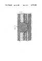
- FIG. 1is a perspective, cut-away view of a typical multilayer structure which may be fabricated in accordance with the invention.
- FIGS. 2-3are cross-sectional views of the multilayer structure of FIG. 1 during different stages of fabrication in accordance with one embodiment of the invention.
- FIG. 1illustrates a typical cavity multilayer board which can be fabricated in accordance with the invention.
- the bottom substrate layer, 10, in this example,is a mixture of bismaleimide, triazine and epoxy, and includes conductive elements, e.g., 11 and 12, on both major surfaces. Also included on the substrate is a conductive pad 13 for bonding a semiconductor chip thereto (not shown).
- Multiple layers, 15 and 16,are located over and properly registered with the substrate, 10. These layers are typically the same type of printed wiring board laminate material as the substrate and also include conductive members on both major surfaces, e.g., 17 and 18, as well as via holes, e.g., 19, electrically connecting the conductors on opposite surfaces.
- the multiple layers, 15 and 16define a cavity, 20, for placement of the chip.
- the cavitytypically measures approximately 0.9 cm ⁇ 1.2 cm at its base and 1.0 cm ⁇ 1.3 cm at the top with a height of 0.065 cm.
- Conductive pads, e.g., 21 and 22,are included on the top surfaces of the two layers, 15 and 16, near the edges defining the cavity so that electrical connections can be made to the chip by wire bonding to the pads.
- Plated through holesare provided through the entire structure so that conductive pins, such as 24 may be inserted therein. These pins provide the electrical connection to the next level of interconnection such as a printed wiring board.
- the multiple layers, 15 and 16are typically bonded to the substrate and to each other by an appropriate adhesive, 25 and 26, provided between the substrate and first layer (15) and between the first and second (16) layers.
- the adhesiveis typically a no flow or low flow, partially polymerized, material which is preimpregnated with glass fabric (known in the art as B-stage prepreg adhesive).
- the adhesivewas a bismaleimide-triazine-expoxy mixture impregnated with E-glass (electrical grade) fabric.
- Other standard adhesivescan be employed.
- Two or more adhesive layersare stacked and aligned in the structure after appropriate cavity cutouts are formed in each layer. Next, heat and pressure are applied to form a permanent bond between the layers.
- the bondingis typically done by increasing the temperature at a rate in the range of 5° C./minute-30° C./minute to a maximum temperature in the range 160°-190° C. which is held for a period of 30-90 minutes.
- the applied pressureis typically, 0.8-4.8 megapascals. This bonding causes the adhesive to flow and can, therefore, result in adhesive flowing into the cavity (including the area over the bonding pads 21).
- FIG. 2illustrates a portion of a multilayer structure during one stage of fabrication in accordance with an embodiment of the invention. It will be appreciated that many packages such as shown in FIG. 1 are batch fabricated from a multilayer board panel which is typically approximately 46 cm ⁇ 61 cm with many cavities formed therein. FIGS. 2 and 3, therefore, show only the portion of the multilayer structure which will eventually result in a single package.
- FIG. 2illustrates the stage where the multiple layers, 15 and 16, have been stacked over the substrate, 10, with the adhesive layers, 25 and 26, provided therebetween, but prior to the lamination operation which will produce final bonding between the layers and substrate.
- a template, 30,is provided on top of the multilayer structure.
- This templateis a thin sheet of material, in this case type 300 stainless steel with a thickness of approximately 0.046 cm, which has openings therein corresponding in size and position to the cavities formed in the multilayer structure.
- the purpose of the templateis to distribute the stresses during the bonding operation to minimize bending of the edges of the layers 15 and 16 which include the bonding pads 21 and 22.
- the templateshould be thin enough not to interfere with the bonding process, but thick enough and with enough bending strength to minimize bending of the layers at the cavity edges. A thickness of 250-750 microns is useful for this function.
- the template materialshould also have a coefficient of thermal expansion similar to the multilayer structure. In addition to stainless steel, a double-clad copper laminate approximately 350 microns thick was suitable.
- a combination of a release film 31 and flowable conformal material 32is provided over the multilayer structure and template.
- the release material, 31, which is in the form of a sheetwas placed on the template, 30, over the entire area of the panel including the portion shown in FIG. 2.
- the conformal material, 32, which was in the form of a tapewas laid on the release film as a series of contiguous stripes approximately 1.3 cm ⁇ 45.7 cm to cover essentially the entire area of the release film.
- the film and materialare placed in contact with the top of the structure (in this case the template) and with each other over the entire area of the structure including all the cavities.
- the release filmis a thin layer of a material which will prevent the conformal material from bonding to the underlying structure.
- the release materialshould also yield at relatively low stress and have high elongation, i.e. be capable of stretching without breaking.
- the release materialhave an elongation of greater than 200 percent with a yield stress of less than 13.8 MPa.
- One useful materialis a fluoropolymer sold by Airtech under the designation Wrightlon 4600.
- Another useful materialis tetrafluoroethylene tape.
- a preferred thicknessis in the range 12.5 microns to 250 microns. If the layer is too thin it will tend to fracture, and if it is too thick, it will not conform to the shape of the cavity. In this example, the thickness was approximately 50 microns.
- the conformal layer, 32should comprise a material which is capable of flowing into and conforming to the dimensions of the chip cavity during the bonding operation to be described.
- the materialshould be capable of flowing into and filling the cavity before the adhesive, 25 and 26, softens and flows into the cavity.
- the materialshould also be thermally stable to withstand the temperature during the bonding operation.
- One useful materialis a butyl rubber sealant tape such as that sold by Airtech under the designation "Airdam”. This is a putty-like material with a viscosity of about 500,000 poise when measured with a Rheometrics Mechanical Spectrometer at a frequency of 1 radian per second and a strain of 15 percent at 25° C.
- a 0.32 cm thick tape of such materialwas utilized.
- a rubber which is flowablei.e. one which is not polymerized or only partially polymerized
- a putty-like consistencyi.e. a viscosity in the range 100,000 to 1,000,000 poise at 25° C.
- thicknesses of the conformal layer within the range 0.13 cm-1.3 cmshould be appropriate. If the layer is too thin, if will not fill the cavity, and if it is too thick, it is not economical.
- the structure in FIG. 2is then subjected to a heat and pressure cycle for bonding the various layers together. That is, in this example, the structure is heated at a rate of 22° C./minute to a peak temperature of 177° C. where it is held for approximately 60 minutes at a pressure of 3.5 MPa in order to fully bond and polymerize the adhesive layers 15 and 16. As shown in FIG. 3, the heat and pressure cause the conformal layer, 32, to flow into and completely fill the cavity.
- the release layer, 31,stretches sufficiently without breaking to provide the necessary interface between the conformal coating and the multilayer structure.
- the conformal layerflows into the cavity prior to the flow of the adhesive layers so that the former acts as a dam against the flow of the latter into the cavity.
- the chip and wire bonding pads, 13 and 21,are therefore protected. Further, since the flow of the adhesive is now prevented, a wider processing window is provided for the bonding operation, both in the choice of adhesives and in the range of laminating cycles. In this example, heating at a rate in the range of 11°-30° C./minute to a peak temperature in the range 160°-190° C. for 30-90 minutes at a pressure of 1.7-4.8 Mpa may be utilized without adverse effects.
- the conformal and release layersare mechanically lifted off the multilayer structure. This is done easily since the release layer prevents sticking of the conformal layer to the structure. The combination of conformal and release materials can then be discarded.
- the template, 30,is also mechanically lifted off the structure and can be reused. Normal processing of the cavity multilayer board, such as fabricating plated through holes (23 of FIG. 1), providing a covercoat (40 of FIG. 1), and assembly of connector pins (24 of FIG. 1) then proceeds.
Landscapes
- Engineering & Computer Science (AREA)
- Manufacturing & Machinery (AREA)
- Microelectronics & Electronic Packaging (AREA)
- Ceramic Engineering (AREA)
- Physics & Mathematics (AREA)
- Condensed Matter Physics & Semiconductors (AREA)
- General Physics & Mathematics (AREA)
- Computer Hardware Design (AREA)
- Power Engineering (AREA)
- Production Of Multi-Layered Print Wiring Board (AREA)
- Ultra Sonic Daignosis Equipment (AREA)
Abstract
Description
Claims (14)
Priority Applications (4)
| Application Number | Priority Date | Filing Date | Title |
|---|---|---|---|
| US06/912,874US4737208A (en) | 1986-09-29 | 1986-09-29 | Method of fabricating multilayer structures with nonplanar surfaces |
| EP87308328AEP0262848A3 (en) | 1986-09-29 | 1987-09-21 | Method of fabricating multilayer structures with nonplanar surfaces |
| CA000548127ACA1275235C (en) | 1986-09-29 | 1987-09-29 | Method of fabricating multilayer structures with nonplanar surfaces |
| JP62242868AJPS6390158A (en) | 1986-09-29 | 1987-09-29 | Method of forming multilayer structure with non-flat surface |
Applications Claiming Priority (1)
| Application Number | Priority Date | Filing Date | Title |
|---|---|---|---|
| US06/912,874US4737208A (en) | 1986-09-29 | 1986-09-29 | Method of fabricating multilayer structures with nonplanar surfaces |
Publications (1)
| Publication Number | Publication Date |
|---|---|
| US4737208Atrue US4737208A (en) | 1988-04-12 |
Family
ID=25432600
Family Applications (1)
| Application Number | Title | Priority Date | Filing Date |
|---|---|---|---|
| US06/912,874Expired - Fee RelatedUS4737208A (en) | 1986-09-29 | 1986-09-29 | Method of fabricating multilayer structures with nonplanar surfaces |
Country Status (4)
| Country | Link |
|---|---|
| US (1) | US4737208A (en) |
| EP (1) | EP0262848A3 (en) |
| JP (1) | JPS6390158A (en) |
| CA (1) | CA1275235C (en) |
Cited By (30)
| Publication number | Priority date | Publication date | Assignee | Title |
|---|---|---|---|---|
| US4808253A (en)* | 1987-11-06 | 1989-02-28 | Grumman Aerospace Corporation | Method and apparatus for performing a repair on a contoured section of a composite structure |
| US4954200A (en)* | 1987-11-10 | 1990-09-04 | The General Electric Company | Method of making drill back-up material for small bore drilling of circuit boards |
| US5116440A (en)* | 1989-08-09 | 1992-05-26 | Risho Kogyo Co., Ltd. | Process for manufacturing multilayer printed wiring board |
| WO1993025385A1 (en)* | 1992-06-12 | 1993-12-23 | Aluminum Company Of America | Method of fabricating multilayer structures with nonplanar surfaces |
| US5283103A (en)* | 1991-09-30 | 1994-02-01 | Aisin Seiki Kabushiki Kaisha | Fiber-reinforced plastic product |
| US5433803A (en)* | 1989-12-05 | 1995-07-18 | Paul N. Van Draanen | Lamination of vegetable matter |
| US5435875A (en)* | 1993-01-27 | 1995-07-25 | Murata Mfg. Co., Ltd. | Method of manufacturing cavitied ceramic multilayer block |
| US5460680A (en)* | 1991-11-08 | 1995-10-24 | Mitsubishi Denki Kabushiki Kaisha | Method for manufacturing multi-layer printed board |
| US5478420A (en)* | 1994-07-28 | 1995-12-26 | International Business Machines Corporation | Process for forming open-centered multilayer ceramic substrates |
| US5530278A (en)* | 1995-04-24 | 1996-06-25 | Xerox Corporation | Semiconductor chip having a dam to prevent contamination of photosensitive structures thereon |
| US5665195A (en)* | 1994-09-14 | 1997-09-09 | International Business Machines Corporation | Apparatus for forming cavities without using an insert |
| US5676788A (en)* | 1996-06-21 | 1997-10-14 | International Business Machines Corporation | Method for forming cavity structures using thermally decomposable surface layer |
| US5683535A (en)* | 1996-07-25 | 1997-11-04 | Northrop Grumman Corporation | Method and apparatus of producing cavities in LTCC substrates |
| US5746874A (en)* | 1995-09-29 | 1998-05-05 | International Business Machines Corporation | Apparatus and method for forming cavity substrates using flexible preform insert |
| US5759320A (en)* | 1997-04-13 | 1998-06-02 | International Business Machines Corporation | Method of forming cavity substrates using compressive pads |
| US5785800A (en)* | 1996-06-21 | 1998-07-28 | International Business Machines Corporation | Apparatus for forming cavity structures using thermally decomposable surface layer |
| US5788808A (en)* | 1997-04-15 | 1998-08-04 | International Business Machines Corporation | Apparatus for forming cavity substrates using compressive pads |
| US5843354A (en)* | 1995-11-21 | 1998-12-01 | General Electric Company | Method for compression molding a fan blade |
| US5855803A (en)* | 1996-11-20 | 1999-01-05 | Northrop Grumman Corporation | Template type cavity-formation device for low temperature cofired ceramic (LTCC) sheets |
| US6270879B1 (en)* | 1999-07-13 | 2001-08-07 | Nitto Denko Corporation | Release member for use in producing a multi-layer printed wiring board |
| US6423174B1 (en) | 1996-06-21 | 2002-07-23 | International Business Machines Corporation | Apparatus and insertless method for forming cavity substrates using coated membrane |
| US6449168B1 (en)* | 1998-10-26 | 2002-09-10 | Telefonaktiebolaget Lm Ericcson (Publ) | Circuit board and a method for manufacturing the same |
| US6527890B1 (en) | 1998-10-09 | 2003-03-04 | Motorola, Inc. | Multilayered ceramic micro-gas chromatograph and method for making the same |
| US6565706B2 (en)* | 2000-06-02 | 2003-05-20 | Nec Electronics Corporation | Support-frame bonding apparatus |
| US6592696B1 (en) | 1998-10-09 | 2003-07-15 | Motorola, Inc. | Method for fabricating a multilayered structure and the structures formed by the method |
| KR100475345B1 (en)* | 2001-03-28 | 2005-03-10 | 가부시키가이샤 무라타 세이사쿠쇼 | Multilayered ceramic substrate production method |
| US20080008847A1 (en)* | 2006-03-01 | 2008-01-10 | Elit Fine Ceramics Co., Ltd. | Led reflector molding process, construction, and loader thereof |
| US20100288540A1 (en)* | 2008-01-18 | 2010-11-18 | Panasonic Corporation | Three-dimensional wiring board |
| US10124534B2 (en)* | 2013-07-18 | 2018-11-13 | Bayerische Motoren Werke Aktiengesellschaft | Adhesive aid and method for adhering components |
| US20240284596A1 (en)* | 2021-09-27 | 2024-08-22 | Chengdu Boe Optoelectronics Technology Co., Ltd. | Circuit board structure and display device |
Families Citing this family (13)
| Publication number | Priority date | Publication date | Assignee | Title |
|---|---|---|---|---|
| EP0265777B1 (en)* | 1986-10-31 | 1993-02-10 | Gte Products Corporation | Method of preparing a ceramic monolithic structure having an internal cavity contained therein |
| EP0276345B1 (en)* | 1987-01-28 | 1993-03-17 | Unisys Corporation | Elastic bladder method of fabricating an integrated circuit package having bonding pads in a stepped cavity |
| GB2222800B (en)* | 1988-09-16 | 1992-02-19 | Stc Plc | Hybrid circuits |
| JP2782734B2 (en)* | 1988-11-02 | 1998-08-06 | 松下電工株式会社 | Multilayer plastic chip carrier |
| JPH0744338B2 (en)* | 1989-08-09 | 1995-05-15 | 利昌工業株式会社 | Manufacturing method of multilayer circuit board for mounting electronic parts |
| CA2036169A1 (en)* | 1990-02-20 | 1991-08-21 | William O. Park | Lamination of integrated circuit packages |
| JP2006179733A (en)* | 2004-12-24 | 2006-07-06 | Casio Comput Co Ltd | Multilayer wiring board and manufacturing method thereof |
| JP5034289B2 (en)* | 2006-03-28 | 2012-09-26 | 大日本印刷株式会社 | Multilayer printed wiring board and manufacturing method thereof |
| JP5082321B2 (en)* | 2006-07-28 | 2012-11-28 | 大日本印刷株式会社 | Multilayer printed wiring board and manufacturing method thereof |
| JP5186927B2 (en)* | 2008-01-18 | 2013-04-24 | パナソニック株式会社 | 3D printed circuit board |
| JP5251212B2 (en)* | 2008-03-31 | 2013-07-31 | パナソニック株式会社 | 3D printed circuit board |
| JP5077679B2 (en)* | 2008-02-29 | 2012-11-21 | 日立化成工業株式会社 | Manufacturing method of bonded substrate |
| CN103745932B (en)* | 2014-01-23 | 2016-04-13 | 无锡江南计算技术研究所 | The manufacture method of WB type base plate for packaging |
Citations (4)
| Publication number | Priority date | Publication date | Assignee | Title |
|---|---|---|---|---|
| US4626309A (en)* | 1984-07-02 | 1986-12-02 | Motorola, Inc. | Selective bonding interconnection mask |
| US4636275A (en)* | 1986-01-21 | 1987-01-13 | Burroughs Corporation | Elastic bladder method of fabricating an integrated circuit package having bonding pads in a stepped cavity |
| US4643935A (en)* | 1986-01-21 | 1987-02-17 | Burroughs Corporation | Epoxy-glass integrated circuit package having bonding pads in a stepped cavity |
| US4680075A (en)* | 1986-01-21 | 1987-07-14 | Unisys Corporation | Thermoplastic plug method of fabricating an integrated circuit package having bonding pads in a stepped cavity |
Family Cites Families (1)
| Publication number | Priority date | Publication date | Assignee | Title |
|---|---|---|---|---|
| US4630172A (en)* | 1983-03-09 | 1986-12-16 | Printed Circuits International | Semiconductor chip carrier package with a heat sink |
- 1986
- 1986-09-29USUS06/912,874patent/US4737208A/ennot_activeExpired - Fee Related
- 1987
- 1987-09-21EPEP87308328Apatent/EP0262848A3/ennot_activeWithdrawn
- 1987-09-29JPJP62242868Apatent/JPS6390158A/enactivePending
- 1987-09-29CACA000548127Apatent/CA1275235C/ennot_activeExpired - Fee Related
Patent Citations (4)
| Publication number | Priority date | Publication date | Assignee | Title |
|---|---|---|---|---|
| US4626309A (en)* | 1984-07-02 | 1986-12-02 | Motorola, Inc. | Selective bonding interconnection mask |
| US4636275A (en)* | 1986-01-21 | 1987-01-13 | Burroughs Corporation | Elastic bladder method of fabricating an integrated circuit package having bonding pads in a stepped cavity |
| US4643935A (en)* | 1986-01-21 | 1987-02-17 | Burroughs Corporation | Epoxy-glass integrated circuit package having bonding pads in a stepped cavity |
| US4680075A (en)* | 1986-01-21 | 1987-07-14 | Unisys Corporation | Thermoplastic plug method of fabricating an integrated circuit package having bonding pads in a stepped cavity |
Non-Patent Citations (4)
| Title |
|---|
| "Fabrication of FR-4 Pin-Grid Arrays", Proceedings of the National Electronic Packaging and Production Conference, Feb. 25-27, 1986, pp. 889-897, Nagy. |
| "Tedlar" PVF Film Technical Bulletin, DuPont Co., No. TD-34 (Jan. 1982). |
| Fabrication of FR 4 Pin Grid Arrays , Proceedings of the National Electronic Packaging and Production Conference, Feb. 25 27, 1986, pp. 889 897, Nagy.* |
| Tedlar PVF Film Technical Bulletin, DuPont Co., No. TD 34 (Jan. 1982).* |
Cited By (40)
| Publication number | Priority date | Publication date | Assignee | Title |
|---|---|---|---|---|
| US4808253A (en)* | 1987-11-06 | 1989-02-28 | Grumman Aerospace Corporation | Method and apparatus for performing a repair on a contoured section of a composite structure |
| US4954200A (en)* | 1987-11-10 | 1990-09-04 | The General Electric Company | Method of making drill back-up material for small bore drilling of circuit boards |
| US5116440A (en)* | 1989-08-09 | 1992-05-26 | Risho Kogyo Co., Ltd. | Process for manufacturing multilayer printed wiring board |
| US5433803A (en)* | 1989-12-05 | 1995-07-18 | Paul N. Van Draanen | Lamination of vegetable matter |
| US5283103A (en)* | 1991-09-30 | 1994-02-01 | Aisin Seiki Kabushiki Kaisha | Fiber-reinforced plastic product |
| US5626713A (en)* | 1991-11-08 | 1997-05-06 | Mitsubishi Denki Kabushiki Kaisha | Method for manufacturing multi-layer printed board |
| US5460680A (en)* | 1991-11-08 | 1995-10-24 | Mitsubishi Denki Kabushiki Kaisha | Method for manufacturing multi-layer printed board |
| WO1993025385A1 (en)* | 1992-06-12 | 1993-12-23 | Aluminum Company Of America | Method of fabricating multilayer structures with nonplanar surfaces |
| US5972140A (en)* | 1992-06-12 | 1999-10-26 | Aluminum Company Of America | Method of fabricating multilayer structures with nonplanar surfaces |
| US5573622A (en)* | 1992-06-12 | 1996-11-12 | Aluminum Company Of America | Apparatus for fabricating multilayer structures |
| US5435875A (en)* | 1993-01-27 | 1995-07-25 | Murata Mfg. Co., Ltd. | Method of manufacturing cavitied ceramic multilayer block |
| US5478420A (en)* | 1994-07-28 | 1995-12-26 | International Business Machines Corporation | Process for forming open-centered multilayer ceramic substrates |
| US5665195A (en)* | 1994-09-14 | 1997-09-09 | International Business Machines Corporation | Apparatus for forming cavities without using an insert |
| US5772837A (en)* | 1994-09-14 | 1998-06-30 | International Business Machines Corporation | Apparatus for forming cavities without using an insert |
| US5530278A (en)* | 1995-04-24 | 1996-06-25 | Xerox Corporation | Semiconductor chip having a dam to prevent contamination of photosensitive structures thereon |
| US5746874A (en)* | 1995-09-29 | 1998-05-05 | International Business Machines Corporation | Apparatus and method for forming cavity substrates using flexible preform insert |
| US5843354A (en)* | 1995-11-21 | 1998-12-01 | General Electric Company | Method for compression molding a fan blade |
| US6423174B1 (en) | 1996-06-21 | 2002-07-23 | International Business Machines Corporation | Apparatus and insertless method for forming cavity substrates using coated membrane |
| US5785800A (en)* | 1996-06-21 | 1998-07-28 | International Business Machines Corporation | Apparatus for forming cavity structures using thermally decomposable surface layer |
| US5676788A (en)* | 1996-06-21 | 1997-10-14 | International Business Machines Corporation | Method for forming cavity structures using thermally decomposable surface layer |
| US5683535A (en)* | 1996-07-25 | 1997-11-04 | Northrop Grumman Corporation | Method and apparatus of producing cavities in LTCC substrates |
| US5855803A (en)* | 1996-11-20 | 1999-01-05 | Northrop Grumman Corporation | Template type cavity-formation device for low temperature cofired ceramic (LTCC) sheets |
| US5759320A (en)* | 1997-04-13 | 1998-06-02 | International Business Machines Corporation | Method of forming cavity substrates using compressive pads |
| US5788808A (en)* | 1997-04-15 | 1998-08-04 | International Business Machines Corporation | Apparatus for forming cavity substrates using compressive pads |
| US6544734B1 (en) | 1998-10-09 | 2003-04-08 | Cynthia G. Briscoe | Multilayered microfluidic DNA analysis system and method |
| US6732567B2 (en) | 1998-10-09 | 2004-05-11 | Motorola, Inc. | Multilayered ceramic micro-gas chromatograph and method for making the same |
| US6527890B1 (en) | 1998-10-09 | 2003-03-04 | Motorola, Inc. | Multilayered ceramic micro-gas chromatograph and method for making the same |
| US6572830B1 (en) | 1998-10-09 | 2003-06-03 | Motorola, Inc. | Integrated multilayered microfludic devices and methods for making the same |
| US6592696B1 (en) | 1998-10-09 | 2003-07-15 | Motorola, Inc. | Method for fabricating a multilayered structure and the structures formed by the method |
| US6449168B1 (en)* | 1998-10-26 | 2002-09-10 | Telefonaktiebolaget Lm Ericcson (Publ) | Circuit board and a method for manufacturing the same |
| US6270879B1 (en)* | 1999-07-13 | 2001-08-07 | Nitto Denko Corporation | Release member for use in producing a multi-layer printed wiring board |
| US6565706B2 (en)* | 2000-06-02 | 2003-05-20 | Nec Electronics Corporation | Support-frame bonding apparatus |
| KR100475345B1 (en)* | 2001-03-28 | 2005-03-10 | 가부시키가이샤 무라타 세이사쿠쇼 | Multilayered ceramic substrate production method |
| US20080008847A1 (en)* | 2006-03-01 | 2008-01-10 | Elit Fine Ceramics Co., Ltd. | Led reflector molding process, construction, and loader thereof |
| US7718024B2 (en)* | 2006-03-01 | 2010-05-18 | Elit Fine Ceramics Co., Ltd. | LED reflector molding process, construction, and loader thereof |
| US20100288540A1 (en)* | 2008-01-18 | 2010-11-18 | Panasonic Corporation | Three-dimensional wiring board |
| US8278565B2 (en) | 2008-01-18 | 2012-10-02 | Panasonic Corporation | Three-dimensional wiring board |
| US10124534B2 (en)* | 2013-07-18 | 2018-11-13 | Bayerische Motoren Werke Aktiengesellschaft | Adhesive aid and method for adhering components |
| US20240284596A1 (en)* | 2021-09-27 | 2024-08-22 | Chengdu Boe Optoelectronics Technology Co., Ltd. | Circuit board structure and display device |
| US12439517B2 (en)* | 2021-09-27 | 2025-10-07 | Chengdu Boe Optoelectronics Technology Co., Ltd. | Circuit board structure and display device |
Also Published As
| Publication number | Publication date |
|---|---|
| EP0262848A3 (en) | 1989-05-10 |
| EP0262848A2 (en) | 1988-04-06 |
| JPS6390158A (en) | 1988-04-21 |
| CA1275235C (en) | 1990-10-16 |
Similar Documents
| Publication | Publication Date | Title |
|---|---|---|
| US4737208A (en) | Method of fabricating multilayer structures with nonplanar surfaces | |
| JP4510020B2 (en) | Manufacturing method of electronic module | |
| US5548091A (en) | Semiconductor chip connection components with adhesives and methods for bonding to the chip | |
| JP6542616B2 (en) | Method of manufacturing component built-in wiring board, component built-in wiring board and tape for fixing electronic component | |
| US4396936A (en) | Integrated circuit chip package with improved cooling means | |
| CN100556233C (en) | Method for manufacturing electronic module and electronic module | |
| US4381602A (en) | Method of mounting an I.C. chip on a substrate | |
| US8399977B2 (en) | Resin-sealed package and method of producing the same | |
| TWI302732B (en) | Embedded chip package process and circuit board with embedded chip | |
| EP1814373A1 (en) | Multilayer printed wiring board and its manufacturing method | |
| US20060166490A1 (en) | Forming buried via hole substrates | |
| CN210579551U (en) | Multilayer wiring board | |
| US20140153204A1 (en) | Electronic component embedded printing circuit board and method for manufacturing the same | |
| JPH09199635A (en) | Multilayer film for forming circuit substrate, multilayer circuit substrate using it, and package for semiconductor device | |
| US10455703B2 (en) | Method for producing a printed circuit board with an embedded sensor chip, and printed circuit board | |
| JP2014146650A (en) | Wiring board and manufacturing method of the same | |
| US6602739B1 (en) | Method for making multichip module substrates by encapsulating electrical conductors and filling gaps | |
| JPH06275742A (en) | Resin-sealed semiconductor device | |
| JP5456113B2 (en) | Resin sealed package | |
| JP2002270744A (en) | Lead frame, method of manufacturing the same, and method of manufacturing heat conductive substrate | |
| JPH0342860A (en) | Flexible printed wiring board | |
| US6755229B2 (en) | Method for preparing high performance ball grid array board and jig applicable to said method | |
| JPH02137293A (en) | multilayer circuit board | |
| JP4408015B2 (en) | Manufacturing method of semiconductor device | |
| JPS6049634A (en) | Manufacture of semiconductor device |
Legal Events
| Date | Code | Title | Description |
|---|---|---|---|
| AS | Assignment | Owner name:BELL TELEPHONE LABORATORIES, INCORPORATED, 600 MOU Free format text:ASSIGNMENT OF ASSIGNORS INTEREST.;ASSIGNORS:BOECHLE, DONALD P.;KALLIAT, MOHANAN P.;REEL/FRAME:004633/0128;SIGNING DATES FROM 19860912 TO 19860916 Owner name:AMERICAN TELEPHONE AND TELEGRAPH COMPANY, 550 MADI Free format text:ASSIGNMENT OF ASSIGNORS INTEREST.;ASSIGNORS:BOECHLE, DONALD P.;KALLIAT, MOHANAN P.;REEL/FRAME:004633/0128;SIGNING DATES FROM 19860912 TO 19860916 Owner name:AT&T TECHNOLOGIES, INCORPORATED, 1 OAK WAY, BERKEL Free format text:ASSIGNMENT OF ASSIGNORS INTEREST.;ASSIGNOR:MAZEIKA, WILLIAM A.;REEL/FRAME:004633/0164 Effective date:19860916 Owner name:AMERICAN TELEPHONE AND TELEGRAPH COMPANY, 550 MADI Free format text:ASSIGNMENT OF ASSIGNORS INTEREST.;ASSIGNOR:MAZEIKA, WILLIAM A.;REEL/FRAME:004633/0164 Effective date:19860916 Owner name:BELL TELEPHONE LABORATORIES, INCORPORATED,NEW JERS Free format text:ASSIGNMENT OF ASSIGNORS INTEREST;ASSIGNORS:BOECHLE, DONALD P.;KALLIAT, MOHANAN P.;SIGNING DATES FROM 19860912 TO 19860916;REEL/FRAME:004633/0128 Owner name:AMERICAN TELEPHONE AND TELEGRAPH COMPANY,NEW YORK Free format text:ASSIGNMENT OF ASSIGNORS INTEREST;ASSIGNORS:BOECHLE, DONALD P.;KALLIAT, MOHANAN P.;SIGNING DATES FROM 19860912 TO 19860916;REEL/FRAME:004633/0128 Owner name:AT&T TECHNOLOGIES, INCORPORATED,NEW JERSEY Free format text:ASSIGNMENT OF ASSIGNORS INTEREST;ASSIGNOR:MAZEIKA, WILLIAM A.;REEL/FRAME:004633/0164 Effective date:19860916 Owner name:AMERICAN TELEPHONE AND TELEGRAPH COMPANY,NEW YORK Free format text:ASSIGNMENT OF ASSIGNORS INTEREST;ASSIGNOR:MAZEIKA, WILLIAM A.;REEL/FRAME:004633/0164 Effective date:19860916 | |
| FEPP | Fee payment procedure | Free format text:PAYOR NUMBER ASSIGNED (ORIGINAL EVENT CODE: ASPN); ENTITY STATUS OF PATENT OWNER: LARGE ENTITY | |
| FPAY | Fee payment | Year of fee payment:4 | |
| FPAY | Fee payment | Year of fee payment:8 | |
| FEPP | Fee payment procedure | Free format text:PAYER NUMBER DE-ASSIGNED (ORIGINAL EVENT CODE: RMPN); ENTITY STATUS OF PATENT OWNER: LARGE ENTITY Free format text:PAYOR NUMBER ASSIGNED (ORIGINAL EVENT CODE: ASPN); ENTITY STATUS OF PATENT OWNER: LARGE ENTITY | |
| REMI | Maintenance fee reminder mailed | ||
| LAPS | Lapse for failure to pay maintenance fees | ||
| FP | Lapsed due to failure to pay maintenance fee | Effective date:20000412 | |
| STCH | Information on status: patent discontinuation | Free format text:PATENT EXPIRED DUE TO NONPAYMENT OF MAINTENANCE FEES UNDER 37 CFR 1.362 |