US4736424A - Data scrambling apparatus - Google Patents
Data scrambling apparatusDownload PDFInfo
- Publication number
- US4736424A US4736424AUS06/910,570US91057086AUS4736424AUS 4736424 AUS4736424 AUS 4736424AUS 91057086 AUS91057086 AUS 91057086AUS 4736424 AUS4736424 AUS 4736424A
- Authority
- US
- United States
- Prior art keywords
- data
- output
- logic
- input
- bit
- Prior art date
- Legal status (The legal status is an assumption and is not a legal conclusion. Google has not performed a legal analysis and makes no representation as to the accuracy of the status listed.)
- Expired - Lifetime
Links
Images
Classifications
- H—ELECTRICITY
- H04—ELECTRIC COMMUNICATION TECHNIQUE
- H04L—TRANSMISSION OF DIGITAL INFORMATION, e.g. TELEGRAPHIC COMMUNICATION
- H04L25/00—Baseband systems
- H04L25/02—Details ; arrangements for supplying electrical power along data transmission lines
- H04L25/03—Shaping networks in transmitter or receiver, e.g. adaptive shaping networks
- H04L25/03828—Arrangements for spectral shaping; Arrangements for providing signals with specified spectral properties
- H04L25/03866—Arrangements for spectral shaping; Arrangements for providing signals with specified spectral properties using scrambling
Definitions
- the present inventionis generally related to electronics and more specifically to data scramblers. Even more specifically, the present invention is related to a data scrambler which checks for the possibility of an effective pattern match between the incoming data to be encoded and the current state of the scrambler register and introduces a pattern breaking bit whenever such a pattern is detected.
- a self-synchronizing data scramblersuffers from th possibility of having an effective pattern match between the incoming data to be encoded and the current state of the scrambler register.
- the result of such a matchcauses an output which is no longer scrambled, but has a repetitive pattern.
- the probability of such a matchis dependent upon the data source with the most likely patterns being an all 1's, an all 0's or an alternating 01 or 10 sequence.
- the general method in the prior art of preventing this type for scrambler failureis to provide gates to monitor the register for the suspect patterns, and then either force a modification to the normal register input, or actually change some register bits directly, so as to perturb the pattern.
- the problem with the first mentioned approachis the possibility that the data pattern can still cause the problem to persist with yet a different pattern.
- the second prior art approachrequires access to the individual register bits, and such access is often inconvenient when dealing with integrated circuits.
- the method disclosed hereincircumvents both of the above problems and provides pattern lockup protection independent of the data supplied, and further provides proper descrambling of this data.
- This problemis circumvented in the present invention by monitoring certain (at least two) of the data bits in the storage register, and altering the logic value of the incoming data bit whenever the monitored bits have a prescribed logic value. Further, selected data bits are logically compared in a simultaneous comparison of a plurality of sets, including the presently supplied data bit, and whenever a given set of conditions is detected, the logic value of the data bit as supplied to the storage mean is altered to break the storage register pattern.
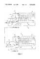
- FIG. 1is a schematic block diagram of a data scrambler and descrambler according to the teachings of the present invention
- FIG. 2is a block schematic diagram of another embodiment of the data scrambler of FIG. 1;
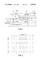
- FIG. 3is a set of logic bit values to be used in explaining the operation of either FIG. 1 or FIG. 2.
- a terminal 10 labeled DATA INsupplies data to one input of an EXCLUSIVE OR gate 12, as well as to an input labeled P7 of a comparator logic element 14.
- An output of EXCLUSIVE OR gate 12appears on a lead 16 and is supplied as scrambled output data to a descrambler generally indicated a 18 and also to an EXCLUSIVE OR gate 20.
- the DATA IN datais labeled for other purposes D, whereas the data on lead 16 is labeled D1.
- the output of EXCLUSIVE OR gate 20is labeled D2, and is supplied to an A input of a storage register means generally designated as 22.
- Storage register 22is illustrated as having eight storage positions, and is a serial-in parallel-out register, of which only seven of the bit positions are used in this embodiment of the invention. It includes a clock input supplied on a lead 24 and has outputs labeled Q1 through 7. Outputs Q1 through 5 of storage means 22 are supplied to corresponding Q inputs of the comparator 14. Output Q6 of register 22 is supplied to inputs P1 and P4 (unlabeled on coaparator 14) and also supplies a first input to an EXCLUSIVE OR gate generally designated a 26. Output Q7 of register 22 is supplied to inputs P0 and unlabeled inputs P3 and P5 of register 14, as well as to a second input of EXCLUSIVE OR gate 26.
- EXCLUSIVE OR gate 26supplies an output on a lead 28, (also labeled as an X bit) and to a second input of EXCLUSIVE OR gate 12.
- the input data 10is shown supplied to a P7 input of comparator 14, while input Q7 of comparator 14 is connected to the Q1 output of storage means 22.
- the comparator 14supplies a logic 0 output if all of the bit sets being compared are alike. In other words, the output is a logic 0 if each of the bit sets are alike, even though different sets may be different logic values. If each of the sets from comparison's 1 through 5 are logic 1's, and Q7 and P7 have logic O's, the output from comparator 14 will still be logic O.
- This outputis inverted by inverter 30 and supplied as a second input PT on lead 32 to EXCLUSIVE OR gate 20.
- the components described so farcomprise a data scrambler generally designated as 34.
- the output of the scrambled datais supplied through one means or another to a descrambler previously designated as 18 on lead 16. This signal is supplied to EXCLUSIVE OR gates 40 and 42.
- the output of EXCLUSIVE OR gate 40comprises descrambled data on lead 44, and this data is also supplied to an input P7 on a comparator 46, which is substantially identical to comparator 14 of scrambler 34.
- the EXCLUSIVE OR gate 42has an output labeled D4 supplied to an input of a storage means or register 48 having a clock input on lead 50 and having 8 data bit storage positions with seven of them being utilized.
- This storage means 48is comparable to storage means 22 of scrambler 34, and is connected to comparator 46 in the identical manner illustrated in connection with scrambler 34.
- the outputs Q6 and Q7are also connected to an EXCLUSIVE OR gate 52 in the same manner as register 22 is connected to EXCLUSIVE OR gate 26.
- An output of EXCLUSIVE OR gate 52is labeled a Y output, and is supplied on a lead 54 to a second input of EXCLUSIVE OR gate 40.
- An output of comparator 46is supplied to an inverter circuit 56 whose output is supplied as a second input to EXCLUSIVE OR gate 42.
- a data input line labeled D and also designated as 75supplies signals to an EXCLUSIVE OR gate 77, as well as to an input on a comparator block 79.
- the comparator block 79is constructed substantially identically to that labeled 14 in FIG. 1. 1t additionally includes an enable input 81.
- An output of EXCLUSIVE OR gate 77is supplied on a lead 83 to an EXCLUSIVE OR gate 85 as well as providing D1 scrambled data output signals.
- An output of EXCLUSIVE OR gate 85is supplied as D2 signals to a storage register 87 shown as having the seven data storage areas corresponding to the seven storage areas utilized in storage register 22 of FIG. 1.
- the register 87has its outputs connected to comparator 79 in a manner substantially identical to that shown in the data scrambler 34 of FIG. 1, although the connections to an EXCLUSIVE OR gate 89 are slightly different than that shown in FIG. 1 for the connections to EXCLUSIVE OR gate 26. Rather, the second data bit position of storage means 87 is connected to one input of EXCLUSIVE OR gate 89, and its other input is obtained from bit position 7 of the storage register 87.
- EXCLUSIVE OR gate 89provides an X output on a lead 91 to a second input of EXCLUSIVE OR gate 77.
- the comparator 79provides output signals indicative of the results of the comparison on all of its inputs to an EXCLUSIVE OR gate 93.
- a second input of EXCLUSIVE OR gate 93is connected to a logic 1 source. As long as the logic 1 source is applied to the second input of EXCLUSIVE OR gate 93, it acts to merely invert any input obtained from comparator 79. An output lead 95 supplies signals PT to a second input of EXCLUSIVE OR gate 85.
- FIG. 3provides indications of the logic value of various points in the circuit.
- the headings D, D1 and D2represent the data at the associated places as does X and PT.
- the register positions 1 through 7represent the corresponding positions in registers 22 or 87.
- the rows of logic values A through Hrepresent the logic values of D1, D2, X and PT given the values of D and the register logic values 1 through 7.
- EXCLUSIVE OR gatewith a logic O on one input gate will merely pass data from the other input to the output with no alteration.
- the datais always inverted as it passes through an EXCLUSIVE OR gate if the other lead of the gate is permanently connected to a logic 1.
- the output data from EXCLUSIVE OR gate 12is always the same as the input data on lead 10, as long as the X output of EXCLUSIVE OR gate 26 remains at a logic 0. Since EXCLUSIVE OR gate 26 is monitoring bit positions 6 and 7 of register 22, it will provide a logic 1 output only when one of bit positions 6 and 7 is a logic 1 and the other is a logic 0.
- the present inventionmonitors or detects the "problem" conditions of the scrambler being locked into a condition where it maintains a continuous series of alternating logic bits regardless of the data input. If the monitored set of logic bits supplied to EXCLUSIVE OR gate 26 are of opposite values, EXCLUSIVE OR gate 12 will alter the value of the output signal 16 relative to data in 10.
- comparator 14provides a logic 1 on the PT output lead 32 whenever all the inputs have a comparison indication of compared logic bits being identical values.
- comparator 14operates to detect one of the four conditions shown in FIG. 3 of all logic 0's as shown in rows A and B, all logic 1's as shown in G or H, or two different combinations of alternating logic values as shown in rows C through F.
- the first comparison in comparator 34is of logic bit 1 and logic bit 7.
- each of these areasprovides a like comparison of two logic 0's or two logic 1's.
- the second comparisonis of logic bit 2 and logic bit 6. This again provides the same like set of values as illustrated in FIG. 3.
- comparison 7the comparison is between the last stored bit in the register 22 and the next bit received to ascertain whether or not the next bit received is of a logic value that will break the problem condition. If it is not of the appropriate logic value to break it, an output will be provided on lead 32 of a logic 1 value to invert D1 to form D2, so that the next bit will result in a stored set of bits that do not perpetuate the problem condition. If the conditions of row A in FIG. 3 are assumed where it is detected that there are all logic 0's in bit positions 1 through 7 of register 22, and the next data bit D on lead 10 is also a logic 0, such a logic bit would perpetuate the "problem" condition of all logic 03 s and be maintained as such.
- the register 22contains alternating values of logic 1 and logic 0 as shown in row C of FIG. 3, and the next incoming data bit is a logic 0, there will be a comparison in the comparator position Q7 P7 of comparator 14, and there will be a logic 1 on lead 32 since the next bit to be entered will have been altered by the logic 1 on lead 28 indicating a lack of comparison in logic values between bit positions 6 and 7 of register 22 as detected by the X bit detector 26. This detected position has already changed the incoming logic 0 on lead 10 to a logic 1 on lead 16, as shown under the caption D1 in FIG. 3.
- comparator 14then returns the logic 1 signal of D1 on lead 16 back to a logic 0 for the D2 output of EXCLUSIVE OR gate 20, so that a logic 0 will be entered on the next clock operation, thereby breaking the continuous logic 1/logic 0 alternating bit pattern previously contained in register 22.
- a logic 1were applied on lead 10
- the descrambler 18 of FIG. 1operates on very similar logic even though the circuitry is not the mirror image of that for scrambler 34. The same reasoning is utilized and the same logic process will prove to anyone skilled in the art that it does descramble the signal to provide an output on 44 which is identical to that previously supplied to data input lead 10.
- comparatorscan be cascaded as can the registers for storing the information.
- the input 81 of FIG. 2would receive the output data from the comparator in the previous stage, and the data being held in the last bit position of the register section shown in FIG. 2, would be supplied to the first bit position of the following register stage.
- FIG. 2also illustrates that the device used to check two or more of the bit positions does not require adjacent bit positions since they are shown to be checking bit positions 2 and 7 in FIG. 2. This again accomplishes exactly the same end result, and the chart of FIG. 3 can be used equally applicable to FIG. 2 as it was to FIG. 1.
- circuitry illustratedprovides a new and novel way of scrambling data, while detecting conditions that would have caused problems in prior art scramblers, and that these problems are automatically resolved to maintain a scrambled data pattern at the output which can be properly interpreted and descrambled by a remote descrambler, thus allowing downstream synchronizing circuits to remain synchronized and permitting downstream data detectors to detect the prope and appropriate data as originally supplied to the scrambling circuit.
Landscapes
- Engineering & Computer Science (AREA)
- Physics & Mathematics (AREA)
- Spectroscopy & Molecular Physics (AREA)
- Power Engineering (AREA)
- Computer Networks & Wireless Communication (AREA)
- Signal Processing (AREA)
- Synchronisation In Digital Transmission Systems (AREA)
Abstract
Description
Claims (5)
Priority Applications (1)
| Application Number | Priority Date | Filing Date | Title |
|---|---|---|---|
| US06/910,570US4736424A (en) | 1986-09-22 | 1986-09-22 | Data scrambling apparatus |
Applications Claiming Priority (1)
| Application Number | Priority Date | Filing Date | Title |
|---|---|---|---|
| US06/910,570US4736424A (en) | 1986-09-22 | 1986-09-22 | Data scrambling apparatus |
Publications (1)
| Publication Number | Publication Date |
|---|---|
| US4736424Atrue US4736424A (en) | 1988-04-05 |
Family
ID=25429003
Family Applications (1)
| Application Number | Title | Priority Date | Filing Date |
|---|---|---|---|
| US06/910,570Expired - LifetimeUS4736424A (en) | 1986-09-22 | 1986-09-22 | Data scrambling apparatus |
Country Status (1)
| Country | Link |
|---|---|
| US (1) | US4736424A (en) |
Cited By (26)
| Publication number | Priority date | Publication date | Assignee | Title |
|---|---|---|---|---|
| US4856063A (en)* | 1988-01-27 | 1989-08-08 | Technical Communication Corporation | No-overhead synchronization for cryptographic systems |
| EP0397384A1 (en)* | 1989-05-04 | 1990-11-14 | Nortel Networks Corporation | Sequence synchronisation |
| US5245661A (en)* | 1992-04-21 | 1993-09-14 | Byeong Gi Lee | Distributed sample scrambling system |
| US5323463A (en)* | 1991-12-13 | 1994-06-21 | 3Com Corporation | Method and apparatus for controlling the spectral content of a data stream |
| US5528526A (en)* | 1993-02-02 | 1996-06-18 | Motorola, Inc. | Arbitrary repeating pattern detector |
| GB2296168A (en)* | 1994-12-12 | 1996-06-19 | Grass Valley Group | Scrambling system for serial digital video |
| US5844510A (en)* | 1996-01-26 | 1998-12-01 | Ora Electronics, Inc. | System and method for extracting a data signal encoded onto first and second binary signals |
| US6611928B1 (en)* | 2000-01-07 | 2003-08-26 | Fujitsu Limited | Homo-code continuity proof testing device |
| US20040091106A1 (en)* | 2002-11-07 | 2004-05-13 | Moore Frank H. | Scrambling of data streams having arbitrary data path widths |
| US20060291271A1 (en)* | 2005-06-24 | 2006-12-28 | Nanochip, Inc. | High density data storage devices having servo indicia formed in a patterned media |
| US20070121477A1 (en)* | 2006-06-15 | 2007-05-31 | Nanochip, Inc. | Cantilever with control of vertical and lateral position of contact probe tip |
| US20070290282A1 (en)* | 2006-06-15 | 2007-12-20 | Nanochip, Inc. | Bonded chip assembly with a micro-mover for microelectromechanical systems |
| US20070291623A1 (en)* | 2006-06-15 | 2007-12-20 | Nanochip, Inc. | Cantilever with control of vertical and lateral position of contact probe tip |
| US20080074984A1 (en)* | 2006-09-21 | 2008-03-27 | Nanochip, Inc. | Architecture for a Memory Device |
| US20080232228A1 (en)* | 2007-03-20 | 2008-09-25 | Nanochip, Inc. | Systems and methods of writing and reading a ferro-electric media with a probe tip |
| WO2008088994A3 (en)* | 2007-01-19 | 2008-09-25 | Nanochip Inc | Method and system for improving domain stability in a ferroelectric media |
| US20080316897A1 (en)* | 2007-06-19 | 2008-12-25 | Nanochip, Inc. | Methods of treating a surface of a ferroelectric media |
| US20080318086A1 (en)* | 2007-06-19 | 2008-12-25 | Nanochip, Inc. | Surface-treated ferroelectric media for use in systems for storing information |
| US20090021975A1 (en)* | 2007-07-16 | 2009-01-22 | Valluri Ramana Rao | Method and media for improving ferroelectric domain stability in an information storage device |
| US20090201015A1 (en)* | 2008-02-12 | 2009-08-13 | Nanochip, Inc. | Method and device for detecting ferroelectric polarization |
| US20090213492A1 (en)* | 2008-02-22 | 2009-08-27 | Nanochip, Inc. | Method of improving stability of domain polarization in ferroelectric thin films |
| US20100002563A1 (en)* | 2008-07-01 | 2010-01-07 | Nanochip, Inc. | Media with tetragonally-strained recording layer having improved surface roughness |
| US20100068509A1 (en)* | 2008-09-17 | 2010-03-18 | Nanochip, Inc. | Media having improved surface smoothness and methods for making the same |
| US20100085863A1 (en)* | 2008-10-07 | 2010-04-08 | Nanochip, Inc. | Retuning of ferroelectric media built-in-bias |
| KR20170122825A (en) | 2015-05-20 | 2017-11-06 | 니폰 가야꾸 가부시끼가이샤 | Dye-based polarizing element, and polarizer and liquid crystal display using the same |
| US9949239B2 (en) | 2007-08-08 | 2018-04-17 | Telefonaktiebolaget Lm Ericsson (Publ) | Uplink scrambling during random access |
Citations (5)
| Publication number | Priority date | Publication date | Assignee | Title |
|---|---|---|---|---|
| US3925612A (en)* | 1963-01-30 | 1975-12-09 | Patelhold Patentverwertung | Digital scrambling apparatus for use in pulsed signal transmission |
| US4109856A (en)* | 1975-05-14 | 1978-08-29 | De Staat Der Nederlanden, Te Dezen Vertegenwoordigd Door De Directeur-Generaal Der Posterijen, Telegrafie En Telefonie | Method for transmitting binary signals |
| US4304962A (en)* | 1965-08-25 | 1981-12-08 | Bell Telephone Laboratories, Incorporated | Data scrambler |
| US4434322A (en)* | 1965-08-19 | 1984-02-28 | Racal Data Communications Inc. | Coded data transmission system |
| US4447672A (en)* | 1980-10-06 | 1984-05-08 | Nippon Electric Co., Ltd. | Device for encrypting each input data bit by at least one keying bit decided by a code pattern and a bit pattern of a predetermined number of preceding encrypted bits |
- 1986
- 1986-09-22USUS06/910,570patent/US4736424A/ennot_activeExpired - Lifetime
Patent Citations (5)
| Publication number | Priority date | Publication date | Assignee | Title |
|---|---|---|---|---|
| US3925612A (en)* | 1963-01-30 | 1975-12-09 | Patelhold Patentverwertung | Digital scrambling apparatus for use in pulsed signal transmission |
| US4434322A (en)* | 1965-08-19 | 1984-02-28 | Racal Data Communications Inc. | Coded data transmission system |
| US4304962A (en)* | 1965-08-25 | 1981-12-08 | Bell Telephone Laboratories, Incorporated | Data scrambler |
| US4109856A (en)* | 1975-05-14 | 1978-08-29 | De Staat Der Nederlanden, Te Dezen Vertegenwoordigd Door De Directeur-Generaal Der Posterijen, Telegrafie En Telefonie | Method for transmitting binary signals |
| US4447672A (en)* | 1980-10-06 | 1984-05-08 | Nippon Electric Co., Ltd. | Device for encrypting each input data bit by at least one keying bit decided by a code pattern and a bit pattern of a predetermined number of preceding encrypted bits |
Cited By (31)
| Publication number | Priority date | Publication date | Assignee | Title |
|---|---|---|---|---|
| US4856063A (en)* | 1988-01-27 | 1989-08-08 | Technical Communication Corporation | No-overhead synchronization for cryptographic systems |
| EP0397384A1 (en)* | 1989-05-04 | 1990-11-14 | Nortel Networks Corporation | Sequence synchronisation |
| US5237593A (en)* | 1989-05-04 | 1993-08-17 | Stc, Plc | Sequence synchronisation |
| US5323463A (en)* | 1991-12-13 | 1994-06-21 | 3Com Corporation | Method and apparatus for controlling the spectral content of a data stream |
| US5245661A (en)* | 1992-04-21 | 1993-09-14 | Byeong Gi Lee | Distributed sample scrambling system |
| US5528526A (en)* | 1993-02-02 | 1996-06-18 | Motorola, Inc. | Arbitrary repeating pattern detector |
| GB2296168A (en)* | 1994-12-12 | 1996-06-19 | Grass Valley Group | Scrambling system for serial digital video |
| GB2296168B (en)* | 1994-12-12 | 1999-03-17 | Grass Valley Group | Scrambling system for serial digital video |
| US5844510A (en)* | 1996-01-26 | 1998-12-01 | Ora Electronics, Inc. | System and method for extracting a data signal encoded onto first and second binary signals |
| US6611928B1 (en)* | 2000-01-07 | 2003-08-26 | Fujitsu Limited | Homo-code continuity proof testing device |
| US20040091106A1 (en)* | 2002-11-07 | 2004-05-13 | Moore Frank H. | Scrambling of data streams having arbitrary data path widths |
| US20060291271A1 (en)* | 2005-06-24 | 2006-12-28 | Nanochip, Inc. | High density data storage devices having servo indicia formed in a patterned media |
| US20070291623A1 (en)* | 2006-06-15 | 2007-12-20 | Nanochip, Inc. | Cantilever with control of vertical and lateral position of contact probe tip |
| US20070121477A1 (en)* | 2006-06-15 | 2007-05-31 | Nanochip, Inc. | Cantilever with control of vertical and lateral position of contact probe tip |
| US20070290282A1 (en)* | 2006-06-15 | 2007-12-20 | Nanochip, Inc. | Bonded chip assembly with a micro-mover for microelectromechanical systems |
| US20080074984A1 (en)* | 2006-09-21 | 2008-03-27 | Nanochip, Inc. | Architecture for a Memory Device |
| WO2008088994A3 (en)* | 2007-01-19 | 2008-09-25 | Nanochip Inc | Method and system for improving domain stability in a ferroelectric media |
| US20080232228A1 (en)* | 2007-03-20 | 2008-09-25 | Nanochip, Inc. | Systems and methods of writing and reading a ferro-electric media with a probe tip |
| US20080316897A1 (en)* | 2007-06-19 | 2008-12-25 | Nanochip, Inc. | Methods of treating a surface of a ferroelectric media |
| US20080318086A1 (en)* | 2007-06-19 | 2008-12-25 | Nanochip, Inc. | Surface-treated ferroelectric media for use in systems for storing information |
| US20090021975A1 (en)* | 2007-07-16 | 2009-01-22 | Valluri Ramana Rao | Method and media for improving ferroelectric domain stability in an information storage device |
| US7626846B2 (en) | 2007-07-16 | 2009-12-01 | Nanochip, Inc. | Method and media for improving ferroelectric domain stability in an information storage device |
| US9949239B2 (en) | 2007-08-08 | 2018-04-17 | Telefonaktiebolaget Lm Ericsson (Publ) | Uplink scrambling during random access |
| US12089218B2 (en) | 2007-08-08 | 2024-09-10 | Telefonaktiebolaget Lm Ericsson (Publ) | Uplink scrambling during random access |
| US11330567B2 (en) | 2007-08-08 | 2022-05-10 | Telefonaktiebolaget Lm Ericsson (Publ) | Uplink scrambling during random access |
| US20090201015A1 (en)* | 2008-02-12 | 2009-08-13 | Nanochip, Inc. | Method and device for detecting ferroelectric polarization |
| US20090213492A1 (en)* | 2008-02-22 | 2009-08-27 | Nanochip, Inc. | Method of improving stability of domain polarization in ferroelectric thin films |
| US20100002563A1 (en)* | 2008-07-01 | 2010-01-07 | Nanochip, Inc. | Media with tetragonally-strained recording layer having improved surface roughness |
| US20100068509A1 (en)* | 2008-09-17 | 2010-03-18 | Nanochip, Inc. | Media having improved surface smoothness and methods for making the same |
| US20100085863A1 (en)* | 2008-10-07 | 2010-04-08 | Nanochip, Inc. | Retuning of ferroelectric media built-in-bias |
| KR20170122825A (en) | 2015-05-20 | 2017-11-06 | 니폰 가야꾸 가부시끼가이샤 | Dye-based polarizing element, and polarizer and liquid crystal display using the same |
Similar Documents
| Publication | Publication Date | Title |
|---|---|---|
| US4736424A (en) | Data scrambling apparatus | |
| US5357249A (en) | Apparatus and method for high speed flexible multiplexing for fiber optic data transmissions | |
| US5307409A (en) | Apparatus and method for fault detection on redundant signal lines via encryption | |
| US3810111A (en) | Data coding with stable base line for recording and transmitting binary data | |
| EP0443754A2 (en) | Method and apparatus for detecting a frame alignment word in a data stream | |
| KR100263789B1 (en) | Telecommunications system with arbityarv alignment parallel framer | |
| US4563546A (en) | Method for preventing "compromising radiation" | |
| US5179592A (en) | Data scrambler and descrambler capable of preventing continuous bit zeros or ones | |
| US3764981A (en) | System for transmitting 1-bit information having priority level | |
| US3876832A (en) | Digital cryptographic system and method | |
| US5180933A (en) | Programmable digital out-of-lock detector | |
| US4977596A (en) | Cryptographic synchronization recovery by measuring randomness of decrypted data | |
| US3914740A (en) | Error detector for pseudo-random sequence of digits | |
| EP0466224B1 (en) | A method and device for supervising and testing majority voting | |
| US4486883A (en) | Address check system | |
| US5003308A (en) | Serial data receiver with phase shift detection | |
| US6192093B1 (en) | Enhanced CIMT coding system and method with automatic word alignment for simplex operation | |
| US6425080B1 (en) | Asynchronous Transfer Mode (ATM) cell descrambling circuit | |
| AU611562B2 (en) | Enciphering and deciphering device for high bit-rate transmission systems | |
| US4985901A (en) | Method and device for evaluating the safety margin of a digital video signal | |
| KR0136568B1 (en) | Method and appartus for detecting frame synchronization in mac signals | |
| EP0136735B1 (en) | Arrangement for checking the counting function of counters | |
| KR930008947B1 (en) | Frame detected circuit of digital transmitted apparatus | |
| JP2752654B2 (en) | Data transmission method of scrambled code | |
| US4993070A (en) | Ciphertext to plaintext communications system and method |
Legal Events
| Date | Code | Title | Description |
|---|---|---|---|
| AS | Assignment | Owner name:ROCKWELL INTERNATIONAL CORPORATION Free format text:ASSIGNMENT OF ASSIGNORS INTEREST.;ASSIGNOR:BUSBY, W. RAY;REEL/FRAME:004631/0885 Effective date:19860919 | |
| STCF | Information on status: patent grant | Free format text:PATENTED CASE | |
| FEPP | Fee payment procedure | Free format text:PAYOR NUMBER ASSIGNED (ORIGINAL EVENT CODE: ASPN); ENTITY STATUS OF PATENT OWNER: LARGE ENTITY | |
| AS | Assignment | Owner name:ALCATEL NETWORK SYSTEM INC., Free format text:ASSIGNMENT OF ASSIGNORS INTEREST.;ASSIGNOR:ROCKWELL INTERNATIONAL CORPORAITON, A DE CORP.;REEL/FRAME:005834/0511 Effective date:19910828 Owner name:ALCATEL NETWORK SYSTEM INC., TEXAS Free format text:ASSIGNMENT OF ASSIGNORS INTEREST;ASSIGNOR:ROCKWELL INTERNATIONAL CORPORAITON;REEL/FRAME:005834/0511 Effective date:19910828 | |
| FPAY | Fee payment | Year of fee payment:4 | |
| FPAY | Fee payment | Year of fee payment:8 | |
| FEPP | Fee payment procedure | Free format text:PAYER NUMBER DE-ASSIGNED (ORIGINAL EVENT CODE: RMPN); ENTITY STATUS OF PATENT OWNER: LARGE ENTITY Free format text:PAYOR NUMBER ASSIGNED (ORIGINAL EVENT CODE: ASPN); ENTITY STATUS OF PATENT OWNER: LARGE ENTITY | |
| FPAY | Fee payment | Year of fee payment:12 |