US4736229A - Method of manufacturing flat panel backplanes, display transistors and displays made thereby - Google Patents
Method of manufacturing flat panel backplanes, display transistors and displays made therebyDownload PDFInfo
- Publication number
- US4736229A US4736229AUS06/493,523US49352383AUS4736229AUS 4736229 AUS4736229 AUS 4736229AUS 49352383 AUS49352383 AUS 49352383AUS 4736229 AUS4736229 AUS 4736229A
- Authority
- US
- United States
- Prior art keywords
- gate
- layer
- transistors
- backplane
- electrodes
- Prior art date
- Legal status (The legal status is an assumption and is not a legal conclusion. Google has not performed a legal analysis and makes no representation as to the accuracy of the status listed.)
- Expired - Lifetime
Links
Images


Classifications
- G—PHYSICS
- G02—OPTICS
- G02F—OPTICAL DEVICES OR ARRANGEMENTS FOR THE CONTROL OF LIGHT BY MODIFICATION OF THE OPTICAL PROPERTIES OF THE MEDIA OF THE ELEMENTS INVOLVED THEREIN; NON-LINEAR OPTICS; FREQUENCY-CHANGING OF LIGHT; OPTICAL LOGIC ELEMENTS; OPTICAL ANALOGUE/DIGITAL CONVERTERS
- G02F1/00—Devices or arrangements for the control of the intensity, colour, phase, polarisation or direction of light arriving from an independent light source, e.g. switching, gating or modulating; Non-linear optics
- G02F1/01—Devices or arrangements for the control of the intensity, colour, phase, polarisation or direction of light arriving from an independent light source, e.g. switching, gating or modulating; Non-linear optics for the control of the intensity, phase, polarisation or colour
- G02F1/13—Devices or arrangements for the control of the intensity, colour, phase, polarisation or direction of light arriving from an independent light source, e.g. switching, gating or modulating; Non-linear optics for the control of the intensity, phase, polarisation or colour based on liquid crystals, e.g. single liquid crystal display cells
- G02F1/133—Constructional arrangements; Operation of liquid crystal cells; Circuit arrangements
- G02F1/136—Liquid crystal cells structurally associated with a semi-conducting layer or substrate, e.g. cells forming part of an integrated circuit
- G02F1/1362—Active matrix addressed cells
- G02F1/1368—Active matrix addressed cells in which the switching element is a three-electrode device
- H—ELECTRICITY
- H10—SEMICONDUCTOR DEVICES; ELECTRIC SOLID-STATE DEVICES NOT OTHERWISE PROVIDED FOR
- H10D—INORGANIC ELECTRIC SEMICONDUCTOR DEVICES
- H10D30/00—Field-effect transistors [FET]
- H10D30/60—Insulated-gate field-effect transistors [IGFET]
- H10D30/67—Thin-film transistors [TFT]
- H10D30/6729—Thin-film transistors [TFT] characterised by the electrodes
- H10D30/673—Thin-film transistors [TFT] characterised by the electrodes characterised by the shapes, relative sizes or dispositions of the gate electrodes
- H10D30/6732—Bottom-gate only TFTs
- H—ELECTRICITY
- H10—SEMICONDUCTOR DEVICES; ELECTRIC SOLID-STATE DEVICES NOT OTHERWISE PROVIDED FOR
- H10D—INORGANIC ELECTRIC SEMICONDUCTOR DEVICES
- H10D30/00—Field-effect transistors [FET]
- H10D30/60—Insulated-gate field-effect transistors [IGFET]
- H10D30/67—Thin-film transistors [TFT]
- H10D30/6729—Thin-film transistors [TFT] characterised by the electrodes
- H10D30/6737—Thin-film transistors [TFT] characterised by the electrodes characterised by the electrode materials
- H10D30/6739—Conductor-insulator-semiconductor electrodes
- H—ELECTRICITY
- H10—SEMICONDUCTOR DEVICES; ELECTRIC SOLID-STATE DEVICES NOT OTHERWISE PROVIDED FOR
- H10D—INORGANIC ELECTRIC SEMICONDUCTOR DEVICES
- H10D30/00—Field-effect transistors [FET]
- H10D30/60—Insulated-gate field-effect transistors [IGFET]
- H10D30/67—Thin-film transistors [TFT]
- H10D30/674—Thin-film transistors [TFT] characterised by the active materials
- H10D30/6741—Group IV materials, e.g. germanium or silicon carbide
- H10D30/6743—Silicon
- H10D30/6746—Amorphous silicon
- H—ELECTRICITY
- H10—SEMICONDUCTOR DEVICES; ELECTRIC SOLID-STATE DEVICES NOT OTHERWISE PROVIDED FOR
- H10D—INORGANIC ELECTRIC SEMICONDUCTOR DEVICES
- H10D86/00—Integrated devices formed in or on insulating or conducting substrates, e.g. formed in silicon-on-insulator [SOI] substrates or on stainless steel or glass substrates
- H10D86/40—Integrated devices formed in or on insulating or conducting substrates, e.g. formed in silicon-on-insulator [SOI] substrates or on stainless steel or glass substrates characterised by multiple TFTs
- H10D86/441—Interconnections, e.g. scanning lines
- H—ELECTRICITY
- H10—SEMICONDUCTOR DEVICES; ELECTRIC SOLID-STATE DEVICES NOT OTHERWISE PROVIDED FOR
- H10D—INORGANIC ELECTRIC SEMICONDUCTOR DEVICES
- H10D86/00—Integrated devices formed in or on insulating or conducting substrates, e.g. formed in silicon-on-insulator [SOI] substrates or on stainless steel or glass substrates
- H10D86/40—Integrated devices formed in or on insulating or conducting substrates, e.g. formed in silicon-on-insulator [SOI] substrates or on stainless steel or glass substrates characterised by multiple TFTs
- H10D86/60—Integrated devices formed in or on insulating or conducting substrates, e.g. formed in silicon-on-insulator [SOI] substrates or on stainless steel or glass substrates characterised by multiple TFTs wherein the TFTs are in active matrices
- G—PHYSICS
- G02—OPTICS
- G02F—OPTICAL DEVICES OR ARRANGEMENTS FOR THE CONTROL OF LIGHT BY MODIFICATION OF THE OPTICAL PROPERTIES OF THE MEDIA OF THE ELEMENTS INVOLVED THEREIN; NON-LINEAR OPTICS; FREQUENCY-CHANGING OF LIGHT; OPTICAL LOGIC ELEMENTS; OPTICAL ANALOGUE/DIGITAL CONVERTERS
- G02F1/00—Devices or arrangements for the control of the intensity, colour, phase, polarisation or direction of light arriving from an independent light source, e.g. switching, gating or modulating; Non-linear optics
- G02F1/01—Devices or arrangements for the control of the intensity, colour, phase, polarisation or direction of light arriving from an independent light source, e.g. switching, gating or modulating; Non-linear optics for the control of the intensity, phase, polarisation or colour
- G02F1/13—Devices or arrangements for the control of the intensity, colour, phase, polarisation or direction of light arriving from an independent light source, e.g. switching, gating or modulating; Non-linear optics for the control of the intensity, phase, polarisation or colour based on liquid crystals, e.g. single liquid crystal display cells
- G02F1/133—Constructional arrangements; Operation of liquid crystal cells; Circuit arrangements
- G02F1/136—Liquid crystal cells structurally associated with a semi-conducting layer or substrate, e.g. cells forming part of an integrated circuit
- G02F1/1362—Active matrix addressed cells
- G02F1/136259—Repairing; Defects
- G02F1/136268—Switch defects
- G—PHYSICS
- G02—OPTICS
- G02F—OPTICAL DEVICES OR ARRANGEMENTS FOR THE CONTROL OF LIGHT BY MODIFICATION OF THE OPTICAL PROPERTIES OF THE MEDIA OF THE ELEMENTS INVOLVED THEREIN; NON-LINEAR OPTICS; FREQUENCY-CHANGING OF LIGHT; OPTICAL LOGIC ELEMENTS; OPTICAL ANALOGUE/DIGITAL CONVERTERS
- G02F2202/00—Materials and properties
- G02F2202/10—Materials and properties semiconductor
- G02F2202/103—Materials and properties semiconductor a-Si
Definitions
- the present inventionpertains to an improved flat panel display and method of making same. More particularly, the present invention is directed to a method of making improved flat panel display backplanes and the switching transistors thereon.
- CRTcathode ray tubes
- the flat panel displayspromise lighter weight, less bulk and substantially lower power consumption than CRT's.
- CRT'snearly always suffer from some distortion.
- the CRTfunctions by projecting an electron beam onto a phosphor-coated screen. The beam will cause the spot on which it is focused to glow with an intensity proportional to the intensity of the beam.
- the displayis created by the constantly moving beam causing different spots on the screen to glow with different intensities. Because the electron beam travels a further distance from its stationary source to the edge of the screen than it does to the middle, the beam strikes various points on the screen at different angles with resulting variation in soot size and shape (i.e. distortion).
- circuit elementsare deposited and patterned, generally by photolithography, on a substrate, such as glass.
- the elementsare deposited and etched in stages to build a device having a matrix of perpendicular rows and columns of circuit control lines with a pixel contact and control element between the control line rows and columns.
- the pixel contacthas a medium thereon which is a substance that either glows (active) or changes its response to ambient light (passive) when a threshold voltage is applied across the medium control element.
- the mediumcan be a liquid crystal, electroluminescent or electrochromic materials such as zinc sulfide, a gas plasma of, for example, neon and argon, a dichroic dye, or such other appropriate material or device as will luminesce or otherwise change optical properties in response to the application of voltage thereto. Light is generated or other optical changes occur in the medium in response to the proper voltage applied thereto.
- Each optically active mediumis generally referred to as a picture element or "pixel".
- the circuitry for a flat panel displayis generally designed such that the flat panel timeshares, or multiplexes, digital circuits to feed signals to one row and column control line of the pixels at a time.
- one driving circuitis used for each row or column control line.
- a subthreshold voltagecan be fed to an entire row containing hundreds or thousands of pixels, keeping them all dark or inactive.
- a small additional voltagecan be supplied selectively to particular columns to cause selected pixels to light up or change optical properties.
- the pixelscan be made to glow brighter by applying a larger voltage or current or a longer pulse of voltage or current.
- LCD'sliquid crystal displays
- the displayis substantially transparent when not activated and becomes light absorbing when activated.
- the imageis created on the display by sequentially activating the pixels, row by row, across the display.
- the geometric distortion described above with respect to CRT'sis not a factor in flat panel displays since each pixel sees essentially the same voltage or cur- rent.
- an improved method of manufacturing backplanes for active matrix displaysincluding improved transistors to greatly reduce display defects and provide improved backplane subassemblies for the displays.
- a drive scheme for driving the displaysis also disclosed.
- ITOindium tin oxide
- the transistoris completely formed before the refractory metal is etched off of the pixel ITO to form the pixel contact.
- a dielectricis deposited over the gate or the gate and gate insulator. The dielectric is then etched away only in the central planar portion of the gate region to eliminate any edge shorting. The edge shorting is eliminated since the following layers are deposited only on the planar portion with the edges isolated therefrom.
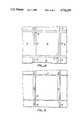
- FIG. 1is a plan view schematic representation of an active matrix display backplane made by a prior art method
- FIG. 2is a cross-section of one transistor of the prior art backplane
- FIG. 3is a plan view schematic representation of one embodiment of a matrix display of the present invention.
- FIG. 4is a first embodiment of a backplane transistor of the present invention taken along the line 4--4 of FIG. 3;
- FIG. 5is a second embodiment of the backplane transistor of the present invention.
- FIGS. 6-10are partial plan views of the display backplane manufacturing steps.
- FIG. 11is a schematic diagram of one embodiment of a matrix display drive circuit.
- FIG. 1there is shown a schematic representation of an active matrix flat panel display device 10 made in accordance with conventional photolithographic techniques.
- One such device 10 and the manufacture thereofis more fully described in Application of Amorphous Silicon Field Effect Transistors in Addressable Liquid Crystal Display Panels, A. J. Snell et al., Applied Physics, No. 24, p. 357, 1981.
- the device 10includes a substrate 12, sets of contact pads 14 and 16, sets of control lines 18 and 20, and, in this particular example of the prior art, transistors 22 and pixel back contacts 24.
- the substrate 12 commonly employed in these devicesis formed from glass.
- the control lines 18 and 20are organized into a matrix of rows 18 and columns 20.
- the control line rows 18 in this device 10serve as gate electrodes and the control line columns 20 as source connections.
- One contact pad 14is connected to each end of the row control lines 18.
- One contact pad 16is connected to each end of the column control lines 20.
- the display drive control(not shown) is connected to the sets of pads 14 and 16.
- transistor 22is formed to connect the row line 18 and column line 20 to the pixel back contacts 24.
- the active mediumis deposited at least on the contacts 24 which will optically change properties in response to the combined voltages or currents in the respective crossover point 26 formed by the row 18 and column 20.
- the active medium at a given crossover point 26will appear as a square or dot in the overall checkerboard type matrix of the display 10.
- the actual size of the transistors 22 and the contacts 24are not now drawn to scale, but are shown schematically for illustration only.
- the problem encountered by the prior art method of manufactureis that if the array of device 10 contains any defective pixel transistors 22 or other circuit elements causing a pixel to be inoperative, it must be discarded.
- the substrate 12is a substantial portion of the backplane cost and hence an inexpensive soda-lime glass is generally utilized. It has been demonstrated by liquid crystal display manufacturers that the high sodium concentration can poison the liquid crystal material by diffusing through the overlying ITO layer and hence an SiO 2 suppression layer 30 is generally formed on the substrate 12. There are some high quality low sodium types of substrates available, which would not need the suppression layer 30.
- An ITO layer 32is formed and etched to provide an ITO free area on which the gate 18 is deposited. Following the deposition of the gate 18, a gate insulator layer 34 is deposited.
- the gate 18has or can have sharp edges which lead to pin holes or thinning of the insulator 34 at the gate edges.
- the source and drain metalscan short to the gate 18.
- the thinning or pin holesproduce transistors 22, which if operative, do not have uniform operating characteristics and hence the backplane is worth- less.
- a second attempt to solve the probemis to make the gate insulator 34 very thick, but this decreases the gain of the transistor 22 and is also self defeating.
- amorphous silicon layer 36is then deposited, with the source 20 and a drain 38 deposited thereover.
- a passivating layer(not shown) would be deposited over the completed structure to complete the transistor 22.
- the activation of the source 20 and the gate 18couples power through the silicon alloy 36 to the drain and hence to the contact pad 24 formed by the ITO layer 32.
- the ITO layer 32is subjected to numerous processing steps, both depositing material and etching the material away. This can lead to nonuniformity of the ITO layer 32 which can also cause the backplane to be defective.
- a matrix display 40 of the present inventionis illustrated schematically in FIG. 3.
- a plurality of transistors 42are each coupled in columns by one of a plurality of gate lines 44 to one of a plurality of gate contact pads 46.
- the transistors 42are each coupled by one of a plurality of source lines 48 to one of a plurality of source gate pads 50.
- Each transistor 42is also coupled to a respective one of a plurality of pixels 52 by a respective drain electrode 54.
- FIG. 4there is shown a schematic representation of one preferred embodiment of the transistor 42 made in accordance with the present invention.
- a glass substrate 56includes a barrier SiO 2 layer 58 thereon. The detailed deposition steps will be described with respect to FIGS. 6-10.
- An ITO layer 60is deposited onto substrate 56 and then a refractory metal layer 62 is deposited on the ITO layer 60.
- ITO layer 60 and metal layer 62are successively deposited (first one layer and then the other) over substrate 56.
- the layers 60 and 62are etched to form the gate electrode 44.
- a gate insulator 64 and a semiconductor material 66are sequentially deposited over the gate 44. That is, insulator 64 is first deposited over gate 44 and then semiconductor layer 66 is deposited over insulator 64 and gate 44.
- the material 66preferably is an amorphous silicon alloy. That is, material 66 preferably is an alloy which has in its composition a greater amount of silicon than any other element. Material 66 may also include hydrogenated silicon, for example.
- a dielectric layer 70is deposited over the gate 44, the gate insulator 64 and the semiconductor 66. The dielectric 70 is deposited to a sufficient thickness to ensure that no shorts or thin spots are formed between the edges 68 of the gate 44 and the source 48 and the drain 54.
- the dielectric 70is etched away only on a substantially planar central region 72 of the semiconductor layer 66. This insures uniform operating characteristics for the transistors 42 in the backplane array.
- a passivating layer 74is deposited over the whole structure to complete the structure of the transistor 42.
- the refractory metal layer 62remains over a pixel contact pad 76 upon which the active material of the pixel 52 is deposited.
- the refractory metalis etched off of the pixel pad 76 leaving the ITO layer 60 exposed after all the processing has been completed.
- FIG. 5An alternate embodiment of the transistor 42' is illustrated in FIG. 5. The major difference is that the dielectric 70' is deposited before the gate insulator 64', but the dielectric 70' performs the same function as in the FIG. 4 embodiment, as does the refractory metal layer 62'.
- Defects in the ITO layer 60 under the gate 44can cause shorts.
- the substrate 56is first cleaned, such as by a dionized water rinse and dried.
- the surface of the substrate 56is then sputter etched which is followed by depositing the SiO 2 layer 58, to a thickness in the range of about 250-2000 ⁇ , and preferably about 500 ⁇ , the ITO layer 60 to a thickness in the range of about 100-500 ⁇ and preferably about 300 ⁇ and then the refractory metal layer 62 to a thickness in the range of 500-2000 ⁇ and preferably about 1000 ⁇ .
- the refractory metal 62is preferably Ni x Cr 1-x , 0 ⁇ X ⁇ 0.8, and preferably Ni 60 Cr 40 .
- Other refractory metals and alloyssuch as Ti, TiW, Mo or Ta can also be utilized to meet the following functions.
- the refractory metal 62shields the ITO layer 60 from the processing gases and etchants to insure that the thickness, integrity, resistivity and optical characteristics of the ITO layer 60 are retained. Therefore the refractory metal must withstand the gas plasmas containing silane (SiH 4 ), which can be at processing temperatures of greater than 200° C. which an unprotected ITO layer 60 will react with.
- SiH 4is generally utilized as one of the gases to produce silicon nitride (Si 3 N 4 ) and hence would attack the ITO layer 32 in forming the prior art transistor 22 (FIG. 2).
- the other steps as described belowinclude metal deposition, plasma etching, chemical etching and photoresist stripping.
- the refractory metal 62must have good adhesion to the ITO layer 60 as well as the gate insulator 64, the dielectric 70 and the drain 54.
- the gate 44provides a required gate light blocking function since the transistor 42 is light sensitive. If light is directed through the other side of the backplane then the passivating layer 74 will include a light blocking material or another light blocking layer will be added.
- the refractory metal 62must be etchable from the ITO layer 60 without effecting it when the structure of the transistor 42 is complete. Further, the refractory metal must serve as a stable gate 44 and should have a low sheet resistivity. For,example, Ni 60 Cr 40 about 1000 ⁇ thick has a sheet resistivity of about 10 ohms/square which is necessary for the long gate lines in the backplane.
- a photoresistis applied to the refractory metal layer 62 which is then soft baked.
- the photoresistis aligned and exposed through a mask and then is developed and hard baked.
- the metal layer 62 and the ITO layer 60are then successively etched, rinsed and dried.
- the photoresistis stripped from the substrate, which is then rinsed and dried leaving the pattern shown in FIG. 6. This leaves a pattern of gates 44, pixel pads 76 (FIG. 4) and contact pads 46 and 50 (FIG. 3).
- the gate insulator 64 and the semiconductor layer 66are now sequentially deposited, preferably in a plasma at a substrate temperature of about 275° C.
- the insulator layer 64preferably is Si 3 N 4 deposited in the range of about 500 to 5000 ⁇ thick and preferably about 2500 ⁇ thick.
- the semiconductor layer 66preferably is an amorphous silicon alloy and is preferably deposited from SiH 4 to a thickness of about 300 to 5000 ⁇ and preferably about 2500 ⁇ .
- a photoresistis spun on, soft baked, aligned, exposed, developed and etched.
- the layers 64 and 66are preferably plasma etched in a carbon tetrafluoride (CF 4 ) plasma. The photoresist is then stripped, rinsed and dried. This results in the active semiconductor areas 66 separated along the lengths of the gates 44 as shown in FIG. 7.
- the dielectric 70is then deposited, preferably in a plasma with a substrate temperature of 250° C.
- the dielectricpreferably is SiO 2 with a thickness in the range of 2000-10,000 ⁇ and preferably about 5000 ⁇ .
- the photoresistis then applied, soft baked, aligned and exposed.
- the resistis then developed out from the areas over the central portion 72 of the semiconductor layer 66, the pixel pads 76 and the gate and source contact pads 46 and 50.
- After hard baking the exposed SiO 2 layeris etched, and then the resist is stripped, rinsed and dried to leave the central portions 72 and the pixel pads 76 exposed as shown in FIG. 8.
- the gate and source contact pads 46 and 50(FIG. 3) are also exposed.
- a plurality of regions 78 between the exposed portions 72 of the semiconductor layer 66are left covered by the dielectric layer 70 which adds additional isolation to the transistors 42 when the source electrodes 48 are deposited over these areas (FIGS. 3 and 9).
- An aluminum alloyis then sputter deposited or evaporated to a thickness in the range of about 500 to 5000 ⁇ and preferably about 2500 ⁇ .
- a photoresistis then applied, soft baked, aligned, exposed, developed and hard baked. The exposed alloy is then etched. The photoresist is then stripped, rinsed and dried to leave the source and drain lines 48 and 54 as shown in FIGS. 3 and 9.
- the passivation layer 74is then deposited, preferably SiO 2 or Si 3 N 4 from a plasma with a substrate temperature of about 250° C to a thickness in the range of 2000 to 10,000 ⁇ and preferably about 5000 ⁇ .
- a photoresistis then applied, soft baked, aligned and exposed.
- the resistis then developed from the gate and source contact pads 46 and 50 and the pixel contact pads 76. After hard baking the passivation layer is then removed from these areas by plasma or buffered oxide etch, rinsed and dried leaving the pattern shown in FIG. 10.
- the pixel contact pads 76 and the gate and source pads 46 and 50are then etched to remove the refractory metal from the ITO layer 60, rinsed and dried.
- the resistis then stripped, rinsed and dried.
- the back planesare then ready to be processed to add the active medium.
- the present inventionprovides a method of manufacturing backplanes for active matrix display devices that radically decreases production costs by substantially increasing the yield of profitable products.
- a drive schemeis illustrated for the completed matrix display 40.
- the backplaneshave the active medium, such as twisted nematic active material, applied between the backplane and a frontplane (not illustrated) which can be another glass substrate.
- the display 40then is connected to a controller 80 by a gate line driver 82 and a source line driver 84.
- the drivers 82 and 84are connected to each respective gate or source line.
- the controller 80provides a gate drive signal over a gate drive line or lines 86 and a source drive signal over a source drive line or lines 88.
- the desired pixelscan then be activated by the controller 80 which also provides a frontplane drive signal on a frontplane line 90.
- a first drive scheme embodimentis illustrated in Table 1.
- the nonselected gate linesare held at the most negative voltage to insure that the transistor will not turn on when the frontplane is alternated.
- the frontplane and source line voltagesare alternated so a constant direct current is not applied to the pixels, since a long term direct current causes the pixel active material to fail very rapidly.
- the voltagescan be alternated at any frequency, but preferably in the range of 30 to 100 hertz.
- the source line for the activated pixelsis alternated and the rest of the voltages are held constant.
- the devicescan be of any desired shape and size.
- any type of thin film semiconductor materialcan be utilized, not just those formed from silane.
- the amorphous silicon alloyscan be deposited from any suitable reaction gas mixture containing at least silicon and hydrogen.
- other semiconductor materialscan be utilized such as cadmium selenide, (CdSe), which can be deposited by sputtering or evaporation processes.
- CdSecadmium selenide
- the substrate 56is described as having a barrier layer 58 thereon, a high quality substrate containing a small amount of or no sodium can be utilized, in which case the barrier layer 58 can be eliminated. It is therefore to be understood that within the scope of the appended claims the invention may be practiced otherwise than as specifically described.
Landscapes
- Physics & Mathematics (AREA)
- Nonlinear Science (AREA)
- Mathematical Physics (AREA)
- Engineering & Computer Science (AREA)
- Chemical & Material Sciences (AREA)
- Crystallography & Structural Chemistry (AREA)
- Microelectronics & Electronic Packaging (AREA)
- General Physics & Mathematics (AREA)
- Optics & Photonics (AREA)
- Liquid Crystal (AREA)
- Thin Film Transistor (AREA)
- Devices For Indicating Variable Information By Combining Individual Elements (AREA)
- Residential Or Office Buildings (AREA)
Abstract
Description
TABLE 1 ______________________________________ V.sub.G V.sub.S V.sub.S V.sub.S Frontplane Write 0 or 1 Write 0Write 1 Non-selected ______________________________________ +10 V +15 V +10 0 -10 V 0 +15 V 0 +10 -10 V ______________________________________
TABLE 2 ______________________________________ V.sub.G V.sub.S V.sub.S V.sub.S Frontplane Write 0 or 1 Write 0Write 1 Non-selected ______________________________________ 0 +15 V 0 +10 V -10 V 0 +15 V 0 -10 V -10 V ______________________________________
Claims (13)
Priority Applications (8)
| Application Number | Priority Date | Filing Date | Title |
|---|---|---|---|
| US06/493,523US4736229A (en) | 1983-05-11 | 1983-05-11 | Method of manufacturing flat panel backplanes, display transistors and displays made thereby |
| DE8484105383TDE3484880D1 (en) | 1983-05-11 | 1984-05-11 | METHOD FOR PRODUCING REAR SIDE PANELS FOR FLAT DISPLAYS OF DISPLAY TRANSISTORS, AND DISPLAYS PRODUCED BY THIS METHOD. |
| AT84105383TATE66095T1 (en) | 1983-05-11 | 1984-05-11 | PROCESS FOR MANUFACTURE OF BACK PLATES FOR FLAT DISPLAY TRANSISTOR DISPLAYS, AND DISPLAYS MANUFACTURED BY THIS PROCESS. |
| EP90202697AEP0411726B1 (en) | 1983-05-11 | 1984-05-11 | A method of manufacturing flat panel display backplanes |
| EP84105383AEP0125666B1 (en) | 1983-05-11 | 1984-05-11 | An improved method of manufacturing flat panel backplanes, display transistors and displays made thereby |
| DE3486325TDE3486325T2 (en) | 1983-05-11 | 1984-05-11 | Process for the production of back panels for flat screens. |
| AT90202697TATE108912T1 (en) | 1983-05-11 | 1984-05-11 | PROCESS FOR MANUFACTURING BACK PANELS FOR FLAT SCREENS. |
| US07/464,933US5123847A (en) | 1983-05-11 | 1990-01-16 | Method of manufacturing flat panel backplanes, display transistors |
Applications Claiming Priority (1)
| Application Number | Priority Date | Filing Date | Title |
|---|---|---|---|
| US06/493,523US4736229A (en) | 1983-05-11 | 1983-05-11 | Method of manufacturing flat panel backplanes, display transistors and displays made thereby |
Related Child Applications (1)
| Application Number | Title | Priority Date | Filing Date |
|---|---|---|---|
| US15092788ADivision | 1983-05-11 | 1988-02-01 |
Publications (1)
| Publication Number | Publication Date |
|---|---|
| US4736229Atrue US4736229A (en) | 1988-04-05 |
Family
ID=23960590
Family Applications (1)
| Application Number | Title | Priority Date | Filing Date |
|---|---|---|---|
| US06/493,523Expired - LifetimeUS4736229A (en) | 1983-05-11 | 1983-05-11 | Method of manufacturing flat panel backplanes, display transistors and displays made thereby |
Country Status (4)
| Country | Link |
|---|---|
| US (1) | US4736229A (en) |
| EP (2) | EP0125666B1 (en) |
| AT (2) | ATE66095T1 (en) |
| DE (2) | DE3486325T2 (en) |
Cited By (16)
| Publication number | Priority date | Publication date | Assignee | Title |
|---|---|---|---|---|
| US4853755A (en)* | 1987-04-23 | 1989-08-01 | Alps Electric Co., Ltd. | Method for manufacturing a thin-film transistor array and a thin-film transistor array manufactured by the method |
| US4942441A (en)* | 1986-03-29 | 1990-07-17 | Hitachi, Ltd. | Thin film semiconductor device and method of manufacturing the same |
| US4961630A (en)* | 1989-03-15 | 1990-10-09 | Ovonic Imaging Systems, Inc. | Liquid crystal display with auxiliary pixel capacitance interconnected through substrate |
| US5017989A (en)* | 1989-12-06 | 1991-05-21 | Xerox Corporation | Solid state radiation sensor array panel |
| US5032531A (en)* | 1988-07-08 | 1991-07-16 | Hitachi, Ltd. | Method of manufacturing active matrix panel |
| US5063421A (en)* | 1988-08-08 | 1991-11-05 | Sharp Kabushiki Kaisha | Silicon carbide light emitting diode having a pn junction |
| US5075244A (en)* | 1989-11-16 | 1991-12-24 | Fuji Xerox Co., Ltd. | Method of manufacturing image sensors |
| US5123847A (en)* | 1983-05-11 | 1992-06-23 | Holmberg Scott H | Method of manufacturing flat panel backplanes, display transistors |
| US5200847A (en)* | 1990-05-01 | 1993-04-06 | Casio Computer Co., Ltd. | Liquid crystal display device having driving circuit forming on a heat-resistant sub-substrate |
| WO1993026139A3 (en)* | 1992-06-11 | 1994-04-14 | United Technologies Corp | Low resistance, thermally stable electrode structure for electroluminescent displays |
| US5362660A (en)* | 1990-10-05 | 1994-11-08 | General Electric Company | Method of making a thin film transistor structure with improved source/drain contacts |
| US6069443A (en)* | 1997-06-23 | 2000-05-30 | Fed Corporation | Passive matrix OLED display |
| US20050263768A1 (en)* | 2004-05-27 | 2005-12-01 | Lg. Philips Lcd Co., Ltd. | Liquid crystal display device and fabricating method thereof |
| US20060081006A1 (en)* | 2004-10-15 | 2006-04-20 | Hannstar Display Corp. | Methods for manufacturing glass and for manufacturing thin film transistor liquid crystal display with lower glass sag |
| WO2007129874A1 (en)* | 2006-05-10 | 2007-11-15 | Lg Chem, Ltd. | Fabrication method for organic electronic device and organic electronic device fabricated by the same method |
| US20090231570A1 (en)* | 2008-03-13 | 2009-09-17 | Aisin Seiki Kabushiki Kaisha, | Concave-convex surface inspection apparatus |
Families Citing this family (12)
| Publication number | Priority date | Publication date | Assignee | Title |
|---|---|---|---|---|
| US4646424A (en)* | 1985-08-02 | 1987-03-03 | General Electric Company | Deposition and hardening of titanium gate electrode material for use in inverted thin film field effect transistors |
| EP0211402B1 (en)* | 1985-08-02 | 1991-05-08 | General Electric Company | Process and structure for thin film transistor matrix addressed liquid crystal displays |
| US4855806A (en)* | 1985-08-02 | 1989-08-08 | General Electric Company | Thin film transistor with aluminum contacts and nonaluminum metallization |
| US4933296A (en)* | 1985-08-02 | 1990-06-12 | General Electric Company | N+ amorphous silicon thin film transistors for matrix addressed liquid crystal displays |
| JPS6280626A (en)* | 1985-10-04 | 1987-04-14 | Hosiden Electronics Co Ltd | liquid crystal display element |
| DE3640174A1 (en)* | 1985-11-27 | 1987-06-04 | Sharp Kk | THIN FILM TRANSISTOR ARRANGEMENT |
| JPS62162857U (en)* | 1986-04-02 | 1987-10-16 | ||
| FR2605132B1 (en)* | 1986-10-14 | 1988-12-09 | Thomson Csf | ELECTROOPTIC VISUALIZATION SCREEN WITH CONTROL TRANSISTORS AND METHOD FOR PRODUCING THE SAME |
| JPH0690372B2 (en)* | 1987-08-26 | 1994-11-14 | シャープ株式会社 | Liquid crystal display element |
| US4778258A (en)* | 1987-10-05 | 1988-10-18 | General Electric Company | Protective tab structure for use in the fabrication of matrix addressed thin film transistor liquid crystal displays |
| US5058995A (en)* | 1990-03-15 | 1991-10-22 | Thomson Consumer Electronics, Inc. | Pixel electrode structure for liquid crystal display devices |
| JP2010206154A (en)* | 2009-02-09 | 2010-09-16 | Hitachi Displays Ltd | Display device |
Citations (3)
| Publication number | Priority date | Publication date | Assignee | Title |
|---|---|---|---|---|
| US3675090A (en)* | 1968-11-04 | 1972-07-04 | Energy Conversion Devices Inc | Film deposited semiconductor devices |
| JPS57106084A (en)* | 1980-12-23 | 1982-07-01 | Toshiba Corp | Amorphous silicon diode |
| JPS57205712A (en)* | 1981-06-12 | 1982-12-16 | Seiko Epson Corp | Production of liquid crystal display body |
- 1983
- 1983-05-11USUS06/493,523patent/US4736229A/ennot_activeExpired - Lifetime
- 1984
- 1984-05-11ATAT84105383Tpatent/ATE66095T1/ennot_activeIP Right Cessation
- 1984-05-11DEDE3486325Tpatent/DE3486325T2/ennot_activeExpired - Fee Related
- 1984-05-11EPEP84105383Apatent/EP0125666B1/ennot_activeExpired - Lifetime
- 1984-05-11EPEP90202697Apatent/EP0411726B1/ennot_activeExpired - Lifetime
- 1984-05-11DEDE8484105383Tpatent/DE3484880D1/ennot_activeExpired - Fee Related
- 1984-05-11ATAT90202697Tpatent/ATE108912T1/ennot_activeIP Right Cessation
Patent Citations (3)
| Publication number | Priority date | Publication date | Assignee | Title |
|---|---|---|---|---|
| US3675090A (en)* | 1968-11-04 | 1972-07-04 | Energy Conversion Devices Inc | Film deposited semiconductor devices |
| JPS57106084A (en)* | 1980-12-23 | 1982-07-01 | Toshiba Corp | Amorphous silicon diode |
| JPS57205712A (en)* | 1981-06-12 | 1982-12-16 | Seiko Epson Corp | Production of liquid crystal display body |
Non-Patent Citations (6)
| Title |
|---|
| 1982, SID Intl. Symposium Digest of Technical Papers, pp. 40 41 by Okubo et al., May 1982.* |
| 1982, SID Intl. Symposium Digest of Technical Papers, pp. 40-41 by Okubo et al., May 1982. |
| IBM Technical Disclosure Bulletin, vol. 21, #4, pp. 1666-1667, Sep. 1978 by Chapman. |
| IBM Technical Disclosure Bulletin, vol. 21, 4, pp. 1666 1667, Sep. 1978 by Chapman.* |
| Snell et al., "Application of Amorphous Silicon Field Effect Transistors in Addressable LCD Panels," Appl. Phys. 24, 357-362 (1981). |
| Snell et al., Application of Amorphous Silicon Field Effect Transistors in Addressable LCD Panels, Appl. Phys. 24, 357 362 (1981).* |
Cited By (25)
| Publication number | Priority date | Publication date | Assignee | Title |
|---|---|---|---|---|
| US5123847A (en)* | 1983-05-11 | 1992-06-23 | Holmberg Scott H | Method of manufacturing flat panel backplanes, display transistors |
| US4942441A (en)* | 1986-03-29 | 1990-07-17 | Hitachi, Ltd. | Thin film semiconductor device and method of manufacturing the same |
| US4853755A (en)* | 1987-04-23 | 1989-08-01 | Alps Electric Co., Ltd. | Method for manufacturing a thin-film transistor array and a thin-film transistor array manufactured by the method |
| US5032531A (en)* | 1988-07-08 | 1991-07-16 | Hitachi, Ltd. | Method of manufacturing active matrix panel |
| US5063421A (en)* | 1988-08-08 | 1991-11-05 | Sharp Kabushiki Kaisha | Silicon carbide light emitting diode having a pn junction |
| US4961630A (en)* | 1989-03-15 | 1990-10-09 | Ovonic Imaging Systems, Inc. | Liquid crystal display with auxiliary pixel capacitance interconnected through substrate |
| US5075244A (en)* | 1989-11-16 | 1991-12-24 | Fuji Xerox Co., Ltd. | Method of manufacturing image sensors |
| US5017989A (en)* | 1989-12-06 | 1991-05-21 | Xerox Corporation | Solid state radiation sensor array panel |
| US5200847A (en)* | 1990-05-01 | 1993-04-06 | Casio Computer Co., Ltd. | Liquid crystal display device having driving circuit forming on a heat-resistant sub-substrate |
| US5362660A (en)* | 1990-10-05 | 1994-11-08 | General Electric Company | Method of making a thin film transistor structure with improved source/drain contacts |
| US5559399A (en)* | 1992-06-11 | 1996-09-24 | Norden Systems, Inc. | Low resistance, thermally stable electrode structure for electroluminescent displays |
| WO1993026139A3 (en)* | 1992-06-11 | 1994-04-14 | United Technologies Corp | Low resistance, thermally stable electrode structure for electroluminescent displays |
| US5445711A (en)* | 1992-06-11 | 1995-08-29 | Westinghouse Norden Systems | Low resistance, thermally stable electrode structure for electroluminescent displays |
| US6069443A (en)* | 1997-06-23 | 2000-05-30 | Fed Corporation | Passive matrix OLED display |
| US20090085040A1 (en)* | 2004-05-27 | 2009-04-02 | Byung Chul Ahn | Liquid crystal display device and fabricating method thereof |
| US20050263768A1 (en)* | 2004-05-27 | 2005-12-01 | Lg. Philips Lcd Co., Ltd. | Liquid crystal display device and fabricating method thereof |
| US8017462B2 (en) | 2004-05-27 | 2011-09-13 | Lg Display Co., Ltd. | Method of making a liquid crystal display device capable of increasing capacitance of storage capacitor |
| US7468527B2 (en)* | 2004-05-27 | 2008-12-23 | Lg Display Co., Ltd. | Liquid crystal display device and fabricating method thereof |
| US20060081006A1 (en)* | 2004-10-15 | 2006-04-20 | Hannstar Display Corp. | Methods for manufacturing glass and for manufacturing thin film transistor liquid crystal display with lower glass sag |
| KR100865445B1 (en) | 2006-05-10 | 2008-10-28 | 주식회사 엘지화학 | Fabrication method for organic electronic device and organic electronic device fabricated by the same method |
| CN101438627B (en)* | 2006-05-10 | 2010-09-08 | Lg化学株式会社 | Method for preparing organic electronic device and organic electronic device prepared by the method |
| WO2007129874A1 (en)* | 2006-05-10 | 2007-11-15 | Lg Chem, Ltd. | Fabrication method for organic electronic device and organic electronic device fabricated by the same method |
| US8338223B2 (en) | 2006-05-10 | 2012-12-25 | Lg Chem, Ltd. | Fabrication method for organic electronic device and organic electronic device fabricated by the same method |
| US20090231570A1 (en)* | 2008-03-13 | 2009-09-17 | Aisin Seiki Kabushiki Kaisha, | Concave-convex surface inspection apparatus |
| US8049868B2 (en) | 2008-03-13 | 2011-11-01 | Aisin Seiki Kabushiki Kaisha | Concave-convex surface inspection apparatus |
Also Published As
| Publication number | Publication date |
|---|---|
| ATE66095T1 (en) | 1991-08-15 |
| DE3486325T2 (en) | 1995-01-19 |
| DE3484880D1 (en) | 1991-09-12 |
| EP0125666A3 (en) | 1986-03-26 |
| EP0411726B1 (en) | 1994-07-20 |
| EP0125666A2 (en) | 1984-11-21 |
| ATE108912T1 (en) | 1994-08-15 |
| EP0411726A3 (en) | 1991-07-03 |
| EP0125666B1 (en) | 1991-08-07 |
| DE3486325D1 (en) | 1994-08-25 |
| EP0411726A2 (en) | 1991-02-06 |
Similar Documents
| Publication | Publication Date | Title |
|---|---|---|
| US4736229A (en) | Method of manufacturing flat panel backplanes, display transistors and displays made thereby | |
| US4545112A (en) | Method of manufacturing thin film transistors and transistors made thereby | |
| US4651185A (en) | Method of manufacturing thin film transistors and transistors made thereby | |
| EP0484842B1 (en) | Flat panel display | |
| US6066506A (en) | TFT, method of making and matrix displays incorporating the TFT | |
| US5019002A (en) | Method of manufacturing flat panel backplanes including electrostatic discharge prevention and displays made thereby | |
| US6160270A (en) | Performance matrix, method of making an active matrix displays incorporating an improved TFT | |
| US4820222A (en) | Method of manufacturing flat panel backplanes including improved testing and yields thereof and displays made thereby | |
| US7115913B2 (en) | Array substrate used for a display device and a method of making the same | |
| EP0136509A2 (en) | Active matrix type display apparatus | |
| US6344377B2 (en) | Liquid crystal display and method of manufacturing the same | |
| JPS6252970A (en) | Method for manufacturing control transistor for panel display screen and control element manufactured based on the method | |
| KR20010015187A (en) | Thin film transistor array and its manufacturing method | |
| US5123847A (en) | Method of manufacturing flat panel backplanes, display transistors | |
| US4810637A (en) | Non-linear control element for a flat electrooptical display screen and a method of fabrication of said control element | |
| US5831694A (en) | TFT panel for high resolution- and large size- liquid crystal display | |
| JP2001511261A (en) | Color filter structure and manufacturing method | |
| US5663575A (en) | Liquid crystal display device providing a high aperture ratio | |
| US5270845A (en) | Liquid crystal display unit manufacturing method including forming one of two gate line layers of display electrode material | |
| US5225364A (en) | Method of fabricating a thin-film transistor matrix for an active matrix display panel | |
| JP2947299B2 (en) | Matrix display device | |
| EP0335724A2 (en) | Thin film transistor array for an electro-optical device and method of manufacturing the same | |
| KR100243813B1 (en) | Liquid crystal display and method for manufacturing the same | |
| JP2905641B2 (en) | Method for manufacturing thin film transistor | |
| JPH04293021A (en) | Manufacturing method of active matrix type liquid crystal display element |
Legal Events
| Date | Code | Title | Description |
|---|---|---|---|
| AS | Assignment | Owner name:ALPHASIL INCORPORATION, 1250 OAKMEAD PKWY., SUITE Free format text:ASSIGNMENT OF ASSIGNORS INTEREST.;ASSIGNORS:HOLMBERG, SCOTT H.;FLASCK, RICHARD A.;REEL/FRAME:004128/0981 Effective date:19830506 | |
| AS | Assignment | Owner name:SPERRY CORPORATION, A CORP OF DE. Free format text:ASSIGNMENT OF 1/2 OF ASSIGNORS INTEREST;ASSIGNOR:ALPHASIL, INC., A CORP OF CA.;REEL/FRAME:004626/0033 Effective date:19860716 | |
| STCF | Information on status: patent grant | Free format text:PATENTED CASE | |
| AS | Assignment | Owner name:HONEYWELL, INC., HONEYWELL PLAZA, MINNEAPOLIS, MN Free format text:ASSIGNMENT OF ASSIGNORS INTEREST. 50% INTEREST;ASSIGNOR:ALPHASIL, INC.;REEL/FRAME:004996/0876 Effective date:19881208 | |
| AS | Assignment | Owner name:HONEYWELL INC., A CORP. OF DE., MINNESOTA Free format text:ASSIGNMENT OF ASSIGNORS INTEREST.;ASSIGNOR:ALPHASIL, INC., A CORP. OF CALIF;REEL/FRAME:005080/0600 Effective date:19890404 | |
| FEPP | Fee payment procedure | Free format text:PAYOR NUMBER ASSIGNED (ORIGINAL EVENT CODE: ASPN); ENTITY STATUS OF PATENT OWNER: LARGE ENTITY | |
| FEPP | Fee payment procedure | Free format text:PAT HLDR NO LONGER CLAIMS SMALL ENT STAT AS SMALL BUSINESS (ORIGINAL EVENT CODE: LSM2); ENTITY STATUS OF PATENT OWNER: LARGE ENTITY Free format text:PAYOR NUMBER ASSIGNED (ORIGINAL EVENT CODE: ASPN); ENTITY STATUS OF PATENT OWNER: LARGE ENTITY Free format text:PAYER NUMBER DE-ASSIGNED (ORIGINAL EVENT CODE: RMPN); ENTITY STATUS OF PATENT OWNER: LARGE ENTITY | |
| FPAY | Fee payment | Year of fee payment:4 | |
| FEPP | Fee payment procedure | Free format text:PAYOR NUMBER ASSIGNED (ORIGINAL EVENT CODE: ASPN); ENTITY STATUS OF PATENT OWNER: LARGE ENTITY Free format text:PAYER NUMBER DE-ASSIGNED (ORIGINAL EVENT CODE: RMPN); ENTITY STATUS OF PATENT OWNER: LARGE ENTITY | |
| FPAY | Fee payment | Year of fee payment:8 | |
| FPAY | Fee payment | Year of fee payment:12 | |
| AS | Assignment | Owner name:LG. PHILIPS LCD CO., LTD., KOREA, DEMOCRATIC PEOPL Free format text:ASSIGNMENT OF ASSIGNORS INTEREST;ASSIGNOR:LG ELECTRONICS, INC.;REEL/FRAME:010281/0291 Effective date:19990921 | |
| AS | Assignment | Owner name:LG.PHILIPS LCD CO., LTD., KOREA, REPUBLIC OF Free format text:ASSIGNMENT OF ASSIGNORS INTEREST;ASSIGNOR:LG ELECTRONICS INC.;REEL/FRAME:020385/0124 Effective date:19990921 | |
| AS | Assignment | Owner name:LG DISPLAY CO., LTD., KOREA, REPUBLIC OF Free format text:CHANGE OF NAME;ASSIGNOR:LG.PHILIPS LCD CO., LTD.;REEL/FRAME:021754/0230 Effective date:20080304 Owner name:LG DISPLAY CO., LTD.,KOREA, REPUBLIC OF Free format text:CHANGE OF NAME;ASSIGNOR:LG.PHILIPS LCD CO., LTD.;REEL/FRAME:021754/0230 Effective date:20080304 |