US4735702A - Method of producing an ISFET and same ISFET - Google Patents
Method of producing an ISFET and same ISFETDownload PDFInfo
- Publication number
- US4735702A US4735702AUS06/807,508US80750885AUS4735702AUS 4735702 AUS4735702 AUS 4735702AUS 80750885 AUS80750885 AUS 80750885AUS 4735702 AUS4735702 AUS 4735702A
- Authority
- US
- United States
- Prior art keywords
- polymer
- coating
- oxide surface
- layer
- metal ion
- Prior art date
- Legal status (The legal status is an assumption and is not a legal conclusion. Google has not performed a legal analysis and makes no representation as to the accuracy of the status listed.)
- Expired - Lifetime
Links
Images

Classifications
- H—ELECTRICITY
- H01—ELECTRIC ELEMENTS
- H01L—SEMICONDUCTOR DEVICES NOT COVERED BY CLASS H10
- H01L21/00—Processes or apparatus adapted for the manufacture or treatment of semiconductor or solid state devices or of parts thereof
- H01L21/02—Manufacture or treatment of semiconductor devices or of parts thereof
- H01L21/02104—Forming layers
- H01L21/02107—Forming insulating materials on a substrate
- H01L21/02109—Forming insulating materials on a substrate characterised by the type of layer, e.g. type of material, porous/non-porous, pre-cursors, mixtures or laminates
- H01L21/02112—Forming insulating materials on a substrate characterised by the type of layer, e.g. type of material, porous/non-porous, pre-cursors, mixtures or laminates characterised by the material of the layer
- H01L21/02118—Forming insulating materials on a substrate characterised by the type of layer, e.g. type of material, porous/non-porous, pre-cursors, mixtures or laminates characterised by the material of the layer carbon based polymeric organic or inorganic material, e.g. polyimides, poly cyclobutene or PVC
- G—PHYSICS
- G01—MEASURING; TESTING
- G01N—INVESTIGATING OR ANALYSING MATERIALS BY DETERMINING THEIR CHEMICAL OR PHYSICAL PROPERTIES
- G01N27/00—Investigating or analysing materials by the use of electric, electrochemical, or magnetic means
- G01N27/26—Investigating or analysing materials by the use of electric, electrochemical, or magnetic means by investigating electrochemical variables; by using electrolysis or electrophoresis
- G01N27/403—Cells and electrode assemblies
- G01N27/414—Ion-sensitive or chemical field-effect transistors, i.e. ISFETS or CHEMFETS
- H—ELECTRICITY
- H10—SEMICONDUCTOR DEVICES; ELECTRIC SOLID-STATE DEVICES NOT OTHERWISE PROVIDED FOR
- H10D—INORGANIC ELECTRIC SEMICONDUCTOR DEVICES
- H10D64/00—Electrodes of devices having potential barriers
- H10D64/60—Electrodes characterised by their materials
- H10D64/66—Electrodes having a conductor capacitively coupled to a semiconductor by an insulator, e.g. MIS electrodes
- H10D64/667—Electrodes having a conductor capacitively coupled to a semiconductor by an insulator, e.g. MIS electrodes the conductor comprising a layer of alloy material, compound material or organic material contacting the insulator, e.g. TiN workfunction layers
- H—ELECTRICITY
- H01—ELECTRIC ELEMENTS
- H01L—SEMICONDUCTOR DEVICES NOT COVERED BY CLASS H10
- H01L21/00—Processes or apparatus adapted for the manufacture or treatment of semiconductor or solid state devices or of parts thereof
- H01L21/02—Manufacture or treatment of semiconductor devices or of parts thereof
- H01L21/02104—Forming layers
- H01L21/02107—Forming insulating materials on a substrate
- H01L21/02225—Forming insulating materials on a substrate characterised by the process for the formation of the insulating layer
- H01L21/0226—Forming insulating materials on a substrate characterised by the process for the formation of the insulating layer formation by a deposition process
- H01L21/02282—Forming insulating materials on a substrate characterised by the process for the formation of the insulating layer formation by a deposition process liquid deposition, e.g. spin-coating, sol-gel techniques, spray coating
Definitions
- the inventionrelates to a method of modifying an oxide surface of a semi-conductor material, incorporated for example in an ISFET, in which a polymer coating is applied to the oxide surface.
- ion sensitive electrodesare used to continuously or otherwise determine positive ions.
- An important requirement to be met by these electrodesis that they have a long life time and are as chemically inert as possible.
- ISFETIon Selective Field Effect Transistor
- the ISFETcomprises semi-conductor material, for example p-type silicon, which is provided with an oxide surface, such as SiO 2 , Al 2 O 3 , Ta 2 O 5 and TiO 2 .
- oxide surfacesuch as SiO 2 , Al 2 O 3 , Ta 2 O 5 and TiO 2 .
- SiO 2 oxide surfacefor example, the working of this pH sensitive ISFET is based on the fact that Si-OH groups can be protonised and deprotonised respectively, depending on the concentration of protons in the environment surrounding the ISFET.
- an ISFETis made which is suitable for the qualitative and quantitative determination of this other positive ion.
- the oxide surfaceis coated with a layer of a polymer or paste containing suitable (macro) cyclic compounds, which preferably possess a high affinity for a particular metal ion, especially in relation to protons.
- the British patent application No. 2.017.400describes the coating of the surface of a gate area of an ISFET with a hydrophobic organic polymer membrane.
- the oxide surface of the semi-conductor materialis treated with a silane coupling agent which couples with the silane groups present on the oxide surface.
- a chemical bond of the hydrophobic organic polymer membrane subsequently to be applied to the treated oxide surfaceis because, according to example 3 of this British publication, the polymer membrane is formed by radical polymerization in the vapour phase, as a result of which the polymer is deposited on the oxide surface of the semi-conductor material physically adheres to it by adsorption.
- the physically adhered membranecould have been removed, according to the state of the art (Journal Polymer Science, part C, 16, p. 2341, 1967), if washed with a solvent (toluene), which could have removed the physically adhered layer.
- a solventtoluene
- the life time of the manufactured IGFETis, as stated, only 24 hours. If it had been a case of a chemically bonded polymer membrane, the life time would have been considerably longer, and in an order of magnitude of at least a number of months.
- the inventionhas for its object the application of a coating on the oxide surface of a semi-conductor material, included for example in an ISFET, as such that this coating is chemically bonded, while such an ISFET is less pH sensitive.
- the silanol groups that have not reactedare generally inaccessible to protons, so that the ISFET becomes less pH sensitive.
- the polymerfor example a polyvinyl, polyamide, polyurethane or polycarbamate
- the polymeris formed from at least one type of monomers which are polymerized to the oxide surface (in this case the oxide surface acts as initiator of the reaction)
- an alkoxy- and/or halogen vinylsilane, aminosilane, isocyanate silaneis reacted with the oxide surface and the silane vinyl, silane epoxy, silane amine groups present on the surface layer are subsequently polymerized with at least one type of vinyl monomers, compounds with more than one alcohol, amine and/or isocyanate group
- the vinyl polymeris a "living" polymer which is chemically bonded on the oxide surface, whereby it is possible to allow an alkoxy and/or halogen vinyl silane to react
- a vinyl polymeris a polymer with a --(CH 2 CHX) n type of chain, where X represents a large number of different substitutes.
- "living" polymersare polymers with a chain end comprising a reactive group which is capable of polymerizing with the same group or with another, for example monomer, group without the addition of an initiator.
- the sensitivity of the ISFET to a particular metal ioncan be obtained, or alternatively increased, if either the polymer is formed out of a second type of monomers which comprises a metal ion complexing group, or a compound comprising a metal ion complexing group is chemically bonded to the polymer, or a second coating of a polymer comprising metal ion complexing groups is appied to the coating of the polymer chemically bonded on the oxide surface.
- the second coatingis chemically bonded to the first coating
- the metal ion complexing groupis a crown ether, a cryptand, podand, spherand and/or an ionopher, whereby in the case of a crown ether, for example, 4'-alkyl-benzo-18-crown-6 has been found to be effective.
- Another aspect of the inventionrelates to a process for manufacturing an ISFET, comprising a semi-conductor material having an oxide surface, where a curable resin is applied over the semi-conductor material and through the resin at least one gate is left open right up to the oxide surface.
- the oxide surfaceis modified with an apolar chemically bonded polymer prior to the application of the resin, so that infiltration of a polar fluid is in very large measure prevented, because the polarity of the modified surface corresponds generally to that of the cured resin.
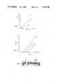
- FIG. 1shows the pH sensitivity of Si plaques where the vertical axis gives the difference in millivolts.
- FIG. 2shows the sensitivity of the modified Si plaques to K + ions.
- FIG. 3shows the stability of the ISFET's.
- FIG. 4shows a section through a combination of a pH ISFET (1) and a metallic ion sensitive ISFET (2).
- a plaque of the semi-conductor material to be treated, which had SiO 2 as its oxide surfacewas heated under reflux for 2 hours in a mixture of 0.5 ml mesitylene.
- the material obtaineddisplayed hydrophobic characteristics.
- the pH sensitivity of the plaque obtained according to example I and IIwas subsequently tested.
- the resultsare shown in FIG. 1 and compared with a non-treated plaque of silicon.
- the line arelates to a non-treated plaque of silicon and shows clearly a continuous variation in the potential on the oxide surface, particularly in the pH area pH 5-7, so that this untreated plaque of silicon is particularly pH sensitive.
- the line brelates to a plaque of silicon, of which the oxide surface, according to example I, is provided with a chemically bonded coating of polystyrene with a thickness of 200 ⁇ .
- line crelates to a plaque of silicon manufactured according to example II.
- this double coatinghas become particularly impermeable for protons. It is in principle possible to give the first and/or second coating a layered build-up.
- ISFETscomprising a plaque of silicon treated according to the invention were measured for different concentrations of K, Li and Cs ions, using 0.15M tetra ethyl ammonium halogenide as reference electrolyte. The measurements are given in the table. pH sensitivity is 23 mV/pH.
- FIG. 3shows the stability of the ISFETs.
- This change in pHcan only result in a small distortion of the measurement results when there are low K + concentrations because of the competition between K + /H + on the surface.
- a non-treated plaque siliconwas heated for 24 hours at 110° C. in a solution of 3-glycidoxy propyl trimethoxy silane in 2 nl of toluene.
- the treated plaquewas agitated for 4 hours at 50° C. in a solution of a poly- or diamine (for example hexane diamine) in toluene.
- a poly- or diaminefor example hexane diamine
- MDI4,4'-diphenyl methane diisocyanate
- a non-treated plaque of siliconwas heated for 24 hours at 110° C. in a solution of 0.3 ml trimethoxy amino propyl silane in 2 ml toluene.
- the treated plaquewas subsequently treated with poly- or diisocyanate and then washed with toluene and treated with a polyamine. This treatment was repeated a number of times until the desired layer thickness was reached.
- the plaques of silicon provided with a chemically bonded polycarbamate or polyurethanecan, in one or a number of treatment steps for the building of the desired layer thickness, additionally and simultaneously be brought into reaction with a ligand having one or a number of isocyanate, amine or alcohol groups. This treatment with the ligand is repeated until the desired degree of saturation of the ligand is reached.
- a non-treated plaque of siliconwas heated in a solution of 0.3 ml trichloro vinyl silane in 2 ml toluene successively for 2 hours at 25° C. and 4 hours at a temperature of 90° C.
- the plaque of siliconwas subsequently washed with toluene and diethylether.
- An alternativewas to bring the non-treated plaque of silicon into contact with thrichloro vinyl silane via the vapour phase and to react the plaque with it.
- the non-treated plaque of siliconwas placed for 24 hours at 300° C. and 0.2 mmHg in a vessel with a gas communicating connection with another vessel holding trichloro vinyl silane.
- the plaque of siliconof which the oxide surface was provided with silane vinyl groups, was placed in a solution of 0.6 ml styrene, 106 mg 4'-vinylbenzo(2.2.2)cryptand and 30 mg dibenzoyl peroxide in 2 ml toluene.
- This solutionwas subsequently twice degassed at 20 mmHg. and then the reaction vessel was filled with nitrogen. The solution was then heated under nitrogen for 24 hours to a temperature of 90° C.
- the plaque of siliconwas then washed with toluene and diethylether and, using ellipsometry, the layer thickness was determined, and this was found to be 200 to 600 ⁇ .
- FIG. 2shows the sensitivity of the modified silicon plaques to K + ions, because the cryptand used (benzo(2.2.2)-cryptand, the line a) and the crown ether (4'-alkyl-benzo-18-crown-6, the lines b and c) have a rather high specific affinity for K + ions.
- the cryptand usedbenzo(2.2.2)-cryptand, the line a
- the crown ether(4'-alkyl-benzo-18-crown-6, the lines b and c
- FIG. 2shows the sensitivity of the modified silicon plaques to K + ions, because the cryptand used (benzo(2.2.2)-cryptand, the line a) and the crown ether (4'-alkyl-benzo-18-crown-6, the lines b and c) have a rather high specific affinity for K + ions.
- such modified silicon plaqueswere found to possess a relatively very low specific affinity for Li + ions.
- Usewas made of a KCl solution
- cryptandscan be considered (see for example Kulstad S. et al Tetrahedron Lett. 21, 643, 1980), as well as crown ethers (Stability and Reactivity of Crown-Ether Complexes, F. de Jong, D. N. Reinhoudt, Academic Press, 1981, London), podands (Vogtle F. et al Angewandte Chemie International Edition English 18, 753, 1979), spherands (Cram, D. J. et al, Journal American Chemical Society 101, 6752, 1979), a variant of spherands, calixa renes (Gutsche C. D. et al, Journal Organic Chemistry 43, 4905, 1978) and ionophors such as Valinomycine (Neupart-Laves, K. et al, Helvetia Chimica Acta, 58, 432, 1975).
- a plaque of siliconwas dried under vacuum for 24 hours at 400° C. 10 ml of a "living" polystyrene solution in tetrahydrofuran (ca. 0.05 mol) was then added under extremely dry conditions. After one hour this solution was quenched with 1 ml methanol and the plaque was washed with tetrahydrofuran and diethylether. The thickness of the applied polystyrene layer amounted to 200 ⁇ .
- a plaque modified as in example Iwas treated for 2 hours at 0° C. under a nitrogen atmosphere and exclusion of moisture with a mixture of 1 g monochloromethyl-methyl ether (ClCH 2 OCH 3 ), 0.25 ml tin tetrachloride (SnCl 4 ) and 3 ml carbon disulphide.
- FIG. 4a section is given through a combination of a pH ISFET 1 and a metallic ion sensitive ISFET 2 which has, for example, specific affinity for Ca 2+ ions.
- Both ISFETs 1, 2comprise a semi-conductor material 3 of the p-type which includes areas 4 of the n-type.
- the surface of the semi-conductor material 3is provided with a coating 5 of an apolar polymer, for example a vinyl polymer, which, according to the invention, is chemically bonded on the oxide surface of the semi-conductor material 3.
- a cured resin 6, for example Aralditeis applied to the coating 5 that is chemically bonded to the semi-conductor material 3 .
- Gates 7, 8 in the resin 6are left open, whereby the part of the coating 5 situated in the area 9 of the gate 7 is removed in a known manner, by etching for example. In this way the gate 7 forms a ion sensitive gate 7.
- a second coating 11 of a polymer comprising crown ether groupsis applied, possibly in multiple layers, by spinning, for example.
- the gate 8forms a metallic ion sensitive gate 8. Accordingly the specificity for a determined metal ion is determined by the choice of crown ether.
- the coating 5is chemically bonded to the layer 3 and has an apolar character, which corresponds inherently with the apolar character of the resin 6, infiltration by polar fluid, for example water, between on the one hand the coating 5 and the semi-conductor material 3 and between on the other hand the coating 5 and the resin 6 is thus prevented. In this way the life time of such an ISFET is increased considerably.
- enzymescan also be bonded covalently on the oxide surface of the semi-conductor material. According to a first embodiment, this can be done be silylating the oxide surface in the previously described ways with a silyl reagent, for example provided with an epoxide group. As a result of the reaction of the enzyme with the epoxide group a structural alteration will occur within the enzyme which results in a decrease of the enzyme activity.
- the enzymecan be complexed via its protonised ammonium groups onto for example crown ethers which are, in the previously described manner, chemically bonded in the polymer applied to the oxide surface layer of the semi-conductor material. In this way it is possible to measure enzyme activity in a solution.
Landscapes
- Engineering & Computer Science (AREA)
- Health & Medical Sciences (AREA)
- Physics & Mathematics (AREA)
- General Physics & Mathematics (AREA)
- Chemical & Material Sciences (AREA)
- Life Sciences & Earth Sciences (AREA)
- Microelectronics & Electronic Packaging (AREA)
- Chemical Kinetics & Catalysis (AREA)
- General Health & Medical Sciences (AREA)
- Computer Hardware Design (AREA)
- Molecular Biology (AREA)
- Manufacturing & Machinery (AREA)
- Condensed Matter Physics & Semiconductors (AREA)
- Electrochemistry (AREA)
- Analytical Chemistry (AREA)
- Biochemistry (AREA)
- Power Engineering (AREA)
- Immunology (AREA)
- Pathology (AREA)
- Addition Polymer Or Copolymer, Post-Treatments, Or Chemical Modifications (AREA)
- Organic Insulating Materials (AREA)
- Treatments Of Macromolecular Shaped Articles (AREA)
- Formation Of Insulating Films (AREA)
- Silicon Polymers (AREA)
- Investigating Or Analyzing Materials By The Use Of Electric Means (AREA)
Abstract
Description
TABLE ______________________________________ Voltage difference as a function of K, Li, Cs ion concentra- tion (constant pH 3 or 9) for ISFET according to the inven- tion. Metal complexing group: 4'-alkyl-benzo-18-crown-6. Voltage difference.sup.(1),(4) (ΔmV/log M.sup.+) Ion I II III IV V ______________________________________ after manufacture.sup.(2) K.sup.+ 4 28 34 37 37 Li.sup.+ 1 3 7 8 9 Cs.sup.+ 3 17 24 27 28 after 40 days.sup.(2) K.sup.+ 4 29 32 39 40 Li.sup.+ 1 3 6 5 7 after 5 months.sup.(3) K.sup.+ 2 15 20 28 33 ______________________________________ .sup.(1) average observations on 8 ISFETs .sup.(2) pH reference electrolyte pH = 9 .sup.(3) pH reference electrolyte pH = 3 .sup.(4) I: 10.sup.-5 - 10.sup.-4 M.sup.+ ; II: 10.sup.-4 - 10.sup.-3 M.sup.+ ; III: 10.sup.-3 - 10.sup.-2 M.sup.+ ; IV: 10.sup.-2 - 10.sup.- M.sup.+ V: 10.sup.-1 - 0.1 M.sup.
Claims (25)
Applications Claiming Priority (2)
| Application Number | Priority Date | Filing Date | Title |
|---|---|---|---|
| NL8400916 | 1984-03-22 | ||
| NL8400916ANL8400916A (en) | 1984-03-22 | 1984-03-22 | METHOD FOR MANUFACTURING AN ISFET AND ISFET MADE THEREFORE |
Publications (1)
| Publication Number | Publication Date |
|---|---|
| US4735702Atrue US4735702A (en) | 1988-04-05 |
Family
ID=19843690
Family Applications (1)
| Application Number | Title | Priority Date | Filing Date |
|---|---|---|---|
| US06/807,508Expired - LifetimeUS4735702A (en) | 1984-03-22 | 1985-03-22 | Method of producing an ISFET and same ISFET |
Country Status (7)
| Country | Link |
|---|---|
| US (1) | US4735702A (en) |
| EP (1) | EP0177544B1 (en) |
| JP (1) | JPS61501726A (en) |
| AT (1) | ATE79472T1 (en) |
| DE (1) | DE3586478T2 (en) |
| NL (1) | NL8400916A (en) |
| WO (1) | WO1985004480A1 (en) |
Cited By (12)
| Publication number | Priority date | Publication date | Assignee | Title |
|---|---|---|---|---|
| US4921591A (en)* | 1987-10-13 | 1990-05-01 | Taiyo Yuden Co., Ltd. | Ion sensors and their divided parts |
| US5035791A (en)* | 1987-07-24 | 1991-07-30 | Eniricerche S.P.A. | Ion sensor containing a selective organic membrane |
| US5087952A (en)* | 1986-11-20 | 1992-02-11 | Biocircuits Corporation | Lipid-protein compositions and articles and methods for their preparation |
| US5130265A (en)* | 1988-12-23 | 1992-07-14 | Eniricerche S.P.A. | Process for obtaining a multifunctional, ion-selective-membrane sensor using a siloxanic prepolymer |
| US5897758A (en)* | 1991-02-04 | 1999-04-27 | Chiron Diagnostics Corporation | Solid contact system for potentiometric sensors |
| US5958201A (en)* | 1996-08-26 | 1999-09-28 | Dade Behring Inc. | Sodium ion-selective-electrode membrane having extended uselife |
| US6525554B2 (en) | 2000-07-20 | 2003-02-25 | National Yunlin University Of Science And Technology | Method and apparatus for measuring temperature parameters of an ISFET using hydrogenated amorphous silicon as a sensing film |
| US20060003438A1 (en)* | 2004-06-17 | 2006-01-05 | Engstrom James R | Growth of inorganic thin films using self-assembled monolayers as nucleation sites |
| US20100109637A1 (en)* | 2006-11-06 | 2010-05-06 | Biowarn, Llc | Sensor system and method |
| US20110156850A1 (en)* | 2008-09-02 | 2011-06-30 | Daisuke Okamoto | Powder for powder magnetic core, powder magnetic core, and methods for producing those producing |
| WO2018106886A1 (en)* | 2016-12-09 | 2018-06-14 | Applied Materials, Inc. | Methods for depositing polymer layer for sensor applications via hot wire chemical vapor deposition |
| US10910284B2 (en)* | 2015-12-08 | 2021-02-02 | Infineon Technologies Austria Ag | Semiconductor device and method of manufacturing thereof |
Families Citing this family (9)
| Publication number | Priority date | Publication date | Assignee | Title |
|---|---|---|---|---|
| NL8602242A (en)* | 1986-09-05 | 1988-04-05 | Stichting Ct Voor Micro Elektr | METHOD FOR MANUFACTURING A REFET OR A CHEMFET, AND THE MANUFACTURED REFET OR CHEMFET |
| JPS63131056A (en)* | 1986-11-20 | 1988-06-03 | Terumo Corp | Fet electrode |
| US5074977A (en)* | 1987-05-05 | 1991-12-24 | The Washington Technology Center | Digital biosensors and method of using same |
| EP0313629A1 (en)* | 1987-05-05 | 1989-05-03 | The Washington Technology Center | A system employing a biosensor to monitor a characteristic of a select component in a medium |
| IT1215491B (en)* | 1987-05-15 | 1990-02-14 | Enricerche Spa | BIOSENSOR WITH ENZYMATIC MEMBRANE CHEMICALLY CONNECTED TO A SEMICONDUCTIVE DEVICE. |
| NL194721C (en)* | 1992-10-15 | 2003-01-07 | Priva Agro Holding Bv | Anion-selective membrane and a sensor provided with it. |
| FR2813208B1 (en)* | 2000-08-30 | 2003-03-28 | Commissariat Energie Atomique | COMPLEXING STRUCTURE, DEVICE AND METHOD FOR TREATING LIQUID EFFLUENTS |
| GB0022360D0 (en)* | 2000-09-13 | 2000-10-25 | British Nuclear Fuels Plc | Improvemnts in and related to sensors |
| US7719004B2 (en) | 2004-02-06 | 2010-05-18 | Micronas Gmbh | Sensor having hydrophobic coated elements |
Citations (3)
| Publication number | Priority date | Publication date | Assignee | Title |
|---|---|---|---|---|
| US3788895A (en)* | 1970-04-21 | 1974-01-29 | Licentia Gmbh | Method for producing a stable surface protection for semiconductor components |
| US4302530A (en)* | 1977-12-08 | 1981-11-24 | University Of Pennsylvania | Method for making substance-sensitive electrical structures by processing substance-sensitive photoresist material |
| US4476003A (en)* | 1983-04-07 | 1984-10-09 | The United States Of America As Represented By The United States Department Of Energy | Chemical anchoring of organic conducting polymers to semiconducting surfaces |
Family Cites Families (6)
| Publication number | Priority date | Publication date | Assignee | Title |
|---|---|---|---|---|
| US4146585A (en)* | 1977-03-02 | 1979-03-27 | Union Carbide Corporation | Process for preparing silane grafted polymers |
| JPS5825221B2 (en)* | 1977-12-12 | 1983-05-26 | 株式会社クラレ | FET reference electrode |
| JPS5853745A (en)* | 1981-09-28 | 1983-03-30 | Hitachi Ltd | 2D electrophoresis device |
| JPS58103656A (en)* | 1981-12-16 | 1983-06-20 | Hitachi Ltd | Device for electrophoresis |
| JPS59210356A (en)* | 1983-05-13 | 1984-11-29 | Kuraray Co Ltd | Triglyceride sensor |
| JPS60177256A (en)* | 1984-02-23 | 1985-09-11 | Shimadzu Corp | Ion sensor |
- 1984
- 1984-03-22NLNL8400916Apatent/NL8400916A/ennot_activeApplication Discontinuation
- 1985
- 1985-03-22WOPCT/NL1985/000013patent/WO1985004480A1/enactiveIP Right Grant
- 1985-03-22ATAT85901604Tpatent/ATE79472T1/ennot_activeIP Right Cessation
- 1985-03-22EPEP85901604Apatent/EP0177544B1/ennot_activeExpired - Lifetime
- 1985-03-22DEDE8585901604Tpatent/DE3586478T2/ennot_activeExpired - Lifetime
- 1985-03-22JPJP60501475Apatent/JPS61501726A/enactivePending
- 1985-03-22USUS06/807,508patent/US4735702A/ennot_activeExpired - Lifetime
Patent Citations (3)
| Publication number | Priority date | Publication date | Assignee | Title |
|---|---|---|---|---|
| US3788895A (en)* | 1970-04-21 | 1974-01-29 | Licentia Gmbh | Method for producing a stable surface protection for semiconductor components |
| US4302530A (en)* | 1977-12-08 | 1981-11-24 | University Of Pennsylvania | Method for making substance-sensitive electrical structures by processing substance-sensitive photoresist material |
| US4476003A (en)* | 1983-04-07 | 1984-10-09 | The United States Of America As Represented By The United States Department Of Energy | Chemical anchoring of organic conducting polymers to semiconducting surfaces |
Non-Patent Citations (2)
| Title |
|---|
| Berg et al., "Sensitivity Control of ISFET's by Chemical Surface Modification", Sensors & Actuators, vol. 8, (1985), pp. 129-148. |
| Berg et al., Sensitivity Control of ISFET s by Chemical Surface Modification , Sensors & Actuators, vol. 8, (1985), pp. 129 148.* |
Cited By (18)
| Publication number | Priority date | Publication date | Assignee | Title |
|---|---|---|---|---|
| US5087952A (en)* | 1986-11-20 | 1992-02-11 | Biocircuits Corporation | Lipid-protein compositions and articles and methods for their preparation |
| US5035791A (en)* | 1987-07-24 | 1991-07-30 | Eniricerche S.P.A. | Ion sensor containing a selective organic membrane |
| US4921591A (en)* | 1987-10-13 | 1990-05-01 | Taiyo Yuden Co., Ltd. | Ion sensors and their divided parts |
| US5130265A (en)* | 1988-12-23 | 1992-07-14 | Eniricerche S.P.A. | Process for obtaining a multifunctional, ion-selective-membrane sensor using a siloxanic prepolymer |
| US5897758A (en)* | 1991-02-04 | 1999-04-27 | Chiron Diagnostics Corporation | Solid contact system for potentiometric sensors |
| US5958201A (en)* | 1996-08-26 | 1999-09-28 | Dade Behring Inc. | Sodium ion-selective-electrode membrane having extended uselife |
| US6525554B2 (en) | 2000-07-20 | 2003-02-25 | National Yunlin University Of Science And Technology | Method and apparatus for measuring temperature parameters of an ISFET using hydrogenated amorphous silicon as a sensing film |
| US6573741B2 (en) | 2000-07-20 | 2003-06-03 | Univ Nat Yunlin Sci & Tech | Apparatus for measuring temperature parameters of an ISFET using hydrogenated amorphous as a sensing film |
| US20060003438A1 (en)* | 2004-06-17 | 2006-01-05 | Engstrom James R | Growth of inorganic thin films using self-assembled monolayers as nucleation sites |
| US7829150B2 (en)* | 2004-06-17 | 2010-11-09 | Cornell Research Foundation, Inc. | Growth of inorganic thin films using self-assembled monolayers as nucleation sites |
| US20100109637A1 (en)* | 2006-11-06 | 2010-05-06 | Biowarn, Llc | Sensor system and method |
| US20110156850A1 (en)* | 2008-09-02 | 2011-06-30 | Daisuke Okamoto | Powder for powder magnetic core, powder magnetic core, and methods for producing those producing |
| CN102132361A (en)* | 2008-09-02 | 2011-07-20 | 丰田自动车株式会社 | Powder for powder magnetic core, powder magnetic core and their manufacturing method |
| US8911866B2 (en)* | 2008-09-02 | 2014-12-16 | Toyota Jidosha Kabushiki Kaisha | Powder for powder magnetic core, powder magnetic core, and methods for producing those products |
| US10910284B2 (en)* | 2015-12-08 | 2021-02-02 | Infineon Technologies Austria Ag | Semiconductor device and method of manufacturing thereof |
| WO2018106886A1 (en)* | 2016-12-09 | 2018-06-14 | Applied Materials, Inc. | Methods for depositing polymer layer for sensor applications via hot wire chemical vapor deposition |
| EP3551780A4 (en)* | 2016-12-09 | 2020-08-05 | Applied Materials, Inc. | METHOD FOR DEPOSITING A POLYMER LAYER FOR SENSOR APPLICATIONS USING CHEMICAL HOT WIRE GAS PHASE DEPOSITION |
| US10794853B2 (en) | 2016-12-09 | 2020-10-06 | Applied Materials, Inc. | Methods for depositing polymer layer for sensor applications via hot wire chemical vapor deposition |
Also Published As
| Publication number | Publication date |
|---|---|
| ATE79472T1 (en) | 1992-08-15 |
| NL8400916A (en) | 1985-10-16 |
| JPS61501726A (en) | 1986-08-14 |
| WO1985004480A1 (en) | 1985-10-10 |
| DE3586478T2 (en) | 1993-02-25 |
| DE3586478D1 (en) | 1992-09-17 |
| EP0177544B1 (en) | 1992-08-12 |
| EP0177544A1 (en) | 1986-04-16 |
Similar Documents
| Publication | Publication Date | Title |
|---|---|---|
| US4735702A (en) | Method of producing an ISFET and same ISFET | |
| van der Wal et al. | New membrane materials for potassium-selective ion-sensitive field-effect transistors | |
| JP2943700B2 (en) | Biosensor | |
| US5445920A (en) | Fabrication process of biosensor | |
| JPS6388439A (en) | Manufacture of ion induction field-effect transistor | |
| Satchwill et al. | Synthesis and characterization of new polyvinylchloride membranes for enhanced adhesion of electrode surfaces | |
| EP0214805A2 (en) | Sensor using a field effect transistor and method of fabricating the same | |
| US5130265A (en) | Process for obtaining a multifunctional, ion-selective-membrane sensor using a siloxanic prepolymer | |
| EP0300575B1 (en) | Ion sensor containing a selective organic membrane | |
| Hanazato et al. | Glucose sensor based on a field-effect transistor with a photolithographically patterned glucose oxidase membrane | |
| JPS61165656A (en) | Formation of immobilized enzyme membrane | |
| Niwa et al. | The interrelation between the electrochemical behaviour of a polymer-coated electrode and the ion exchange properties of the coating | |
| Van der Wal et al. | Universal approach for the fabrication of Ca2+-, K+-and NO3−-sensitive membrane ISFETs | |
| Hanazato et al. | Multi-enzyme electrode using hydrogen-ion-sensitive field-effect transistors | |
| Widrig et al. | Mediated, thin-layer cell, coulometric determination of monomolecular films of trichlorosilane viologen derivatives at gold and nonconducting surfaces | |
| Sakong et al. | Asymmetric membrane-based potentiometric solid-state ion sensors | |
| EP0270174B1 (en) | Ion-sensitive device | |
| JPH0570103B2 (en) | ||
| JPS63217265A (en) | Production of semiconductor ion sensor | |
| JP2563739B2 (en) | Protein immobilization method | |
| WO1991011827A1 (en) | Passivated silicon substrate | |
| EP0555952B1 (en) | PVC coatings for electrodes | |
| JPH051423B2 (en) | ||
| US5637642A (en) | PVC adhesives for electrodes and other applications | |
| JP2002542462A (en) | Method for attaching a PVC adhesive layer to an electrode and an electrode manufactured according to such a method |
Legal Events
| Date | Code | Title | Description |
|---|---|---|---|
| AS | Assignment | Owner name:STICHTING CENTRUM VOOR MICRO-ELECTRONICA TWENTE, N Free format text:ASSIGNMENT OF ASSIGNORS INTEREST.;ASSIGNORS:REINHOUDT, DAVID N.;PENNINGS, MARCEL L. M.;TALMA, AUKE G.;REEL/FRAME:004652/0966 Effective date:19861119 Owner name:STICHTING CENTRUM VOOR MICRO-ELECTRONICA TWENTE, N Free format text:ASSIGNMENT OF ASSIGNORS INTEREST;ASSIGNORS:REINHOUDT, DAVID N.;PENNINGS, MARCEL L. M.;TALMA, AUKE G.;REEL/FRAME:004652/0966 Effective date:19861119 | |
| STCF | Information on status: patent grant | Free format text:PATENTED CASE | |
| CC | Certificate of correction | ||
| REMI | Maintenance fee reminder mailed | ||
| FPAY | Fee payment | Year of fee payment:4 | |
| SULP | Surcharge for late payment | ||
| AS | Assignment | Owner name:PRIVA AGRO HOLDING B.V. Free format text:ASSIGNMENT OF ASSIGNORS INTEREST.;ASSIGNOR:STICHTING CENTRUM VOOR MICRO ELECTRONICA TWENTE, A FOUNDATION OF THE NETHERLANDS;REEL/FRAME:005916/0998 Effective date:19910815 | |
| FEPP | Fee payment procedure | Free format text:PAYOR NUMBER ASSIGNED (ORIGINAL EVENT CODE: ASPN); ENTITY STATUS OF PATENT OWNER: LARGE ENTITY | |
| REMI | Maintenance fee reminder mailed | ||
| FPAY | Fee payment | Year of fee payment:8 | |
| SULP | Surcharge for late payment | ||
| REFU | Refund | Free format text:REFUND - PAYMENT OF MAINTENANCE FEE, 12TH YEAR, LARGE ENTITY (ORIGINAL EVENT CODE: R185); ENTITY STATUS OF PATENT OWNER: LARGE ENTITY | |
| FPAY | Fee payment | Year of fee payment:12 |