US4731340A - Dual lift-off self aligning process for making heterojunction bipolar transistors - Google Patents
Dual lift-off self aligning process for making heterojunction bipolar transistorsDownload PDFInfo
- Publication number
- US4731340A US4731340AUS07/017,957US1795787AUS4731340AUS 4731340 AUS4731340 AUS 4731340AUS 1795787 AUS1795787 AUS 1795787AUS 4731340 AUS4731340 AUS 4731340A
- Authority
- US
- United States
- Prior art keywords
- layer
- conductivity type
- opening
- depositing
- hbt
- Prior art date
- Legal status (The legal status is an assumption and is not a legal conclusion. Google has not performed a legal analysis and makes no representation as to the accuracy of the status listed.)
- Expired - Lifetime
Links
Images
Classifications
- H—ELECTRICITY
- H10—SEMICONDUCTOR DEVICES; ELECTRIC SOLID-STATE DEVICES NOT OTHERWISE PROVIDED FOR
- H10D—INORGANIC ELECTRIC SEMICONDUCTOR DEVICES
- H10D10/00—Bipolar junction transistors [BJT]
- H10D10/01—Manufacture or treatment
- H10D10/021—Manufacture or treatment of heterojunction BJTs [HBT]
- H—ELECTRICITY
- H01—ELECTRIC ELEMENTS
- H01L—SEMICONDUCTOR DEVICES NOT COVERED BY CLASS H10
- H01L21/00—Processes or apparatus adapted for the manufacture or treatment of semiconductor or solid state devices or of parts thereof
- H01L21/02—Manufacture or treatment of semiconductor devices or of parts thereof
- H01L21/027—Making masks on semiconductor bodies for further photolithographic processing not provided for in group H01L21/18 or H01L21/34
- H01L21/0271—Making masks on semiconductor bodies for further photolithographic processing not provided for in group H01L21/18 or H01L21/34 comprising organic layers
- H01L21/0272—Making masks on semiconductor bodies for further photolithographic processing not provided for in group H01L21/18 or H01L21/34 comprising organic layers for lift-off processes
- H—ELECTRICITY
- H10—SEMICONDUCTOR DEVICES; ELECTRIC SOLID-STATE DEVICES NOT OTHERWISE PROVIDED FOR
- H10D—INORGANIC ELECTRIC SEMICONDUCTOR DEVICES
- H10D10/00—Bipolar junction transistors [BJT]
- H10D10/80—Heterojunction BJTs
- H10D10/821—Vertical heterojunction BJTs
- H—ELECTRICITY
- H10—SEMICONDUCTOR DEVICES; ELECTRIC SOLID-STATE DEVICES NOT OTHERWISE PROVIDED FOR
- H10D—INORGANIC ELECTRIC SEMICONDUCTOR DEVICES
- H10D62/00—Semiconductor bodies, or regions thereof, of devices having potential barriers
- H10D62/10—Shapes, relative sizes or dispositions of the regions of the semiconductor bodies; Shapes of the semiconductor bodies
- H10D62/113—Isolations within a component, i.e. internal isolations
- H10D62/115—Dielectric isolations, e.g. air gaps
- H—ELECTRICITY
- H10—SEMICONDUCTOR DEVICES; ELECTRIC SOLID-STATE DEVICES NOT OTHERWISE PROVIDED FOR
- H10D—INORGANIC ELECTRIC SEMICONDUCTOR DEVICES
- H10D62/00—Semiconductor bodies, or regions thereof, of devices having potential barriers
- H10D62/10—Shapes, relative sizes or dispositions of the regions of the semiconductor bodies; Shapes of the semiconductor bodies
- H10D62/13—Semiconductor regions connected to electrodes carrying current to be rectified, amplified or switched, e.g. source or drain regions
- H10D62/137—Collector regions of BJTs
- H—ELECTRICITY
- H10—SEMICONDUCTOR DEVICES; ELECTRIC SOLID-STATE DEVICES NOT OTHERWISE PROVIDED FOR
- H10D—INORGANIC ELECTRIC SEMICONDUCTOR DEVICES
- H10D62/00—Semiconductor bodies, or regions thereof, of devices having potential barriers
- H10D62/80—Semiconductor bodies, or regions thereof, of devices having potential barriers characterised by the materials
- H10D62/85—Semiconductor bodies, or regions thereof, of devices having potential barriers characterised by the materials being Group III-V materials, e.g. GaAs
- Y—GENERAL TAGGING OF NEW TECHNOLOGICAL DEVELOPMENTS; GENERAL TAGGING OF CROSS-SECTIONAL TECHNOLOGIES SPANNING OVER SEVERAL SECTIONS OF THE IPC; TECHNICAL SUBJECTS COVERED BY FORMER USPC CROSS-REFERENCE ART COLLECTIONS [XRACs] AND DIGESTS
- Y10—TECHNICAL SUBJECTS COVERED BY FORMER USPC
- Y10S—TECHNICAL SUBJECTS COVERED BY FORMER USPC CROSS-REFERENCE ART COLLECTIONS [XRACs] AND DIGESTS
- Y10S438/00—Semiconductor device manufacturing: process
- Y10S438/942—Masking
- Y10S438/948—Radiation resist
- Y10S438/951—Lift-off
Definitions
- This inventionrelates to the field of solid state electronics, and particularly to a process for making heterojunction bipolar transistors using a dual lift-off technique to provide self alignment of the emitter and base contacts.
- heterojunction bipolar transistorsIn heterojunction bipolar transistors (HBTs), the intrinsic transistor speed is governed by the vertical layer structure of the device which is incorporated during growth of the wafer. This aspect of the device can be optimized and controlled using molecular beam epitaxy (MBE) or metal organic chemical vapor deposition (MOCVD) growth technology.
- MBEmolecular beam epitaxy
- MOCVDmetal organic chemical vapor deposition
- Subsequent processing of the waferdetermines the lateral extent of the different device regions (emitter area, extrinsic base area, and collector area). Obtaining accurate lateral geometry is important because it determines the magnitude of parasitic extrinsic circuit elements associated with the transistor, notably, base-collector capacitance and base resistance. Currently, these parasitic elements have a major role in determining bipolar circuit speed, particularly in HBTs which are intrinsically extremely fast.
- the dimensions of the transistoralso influence the power dissipation at which the highest speeds are achieved. It is important to reduce the dimension of HBTs in order to both decrease their parasitic elements and to improve their speed-power performance. This requires processing techniques which can accurately produce very small geometry HBTs.
- minimum device dimensionsare determined by three factors: (1) Minimum lithographic feature size, (2) Variations of dimensions as a result of process nonuniformity, and (3) alignment inaccuracies.
- Minimum lithographic feature sizea feature size that can be defined using optical lithography, and dimensions can be reasonably reproduced with available process controls.
- alignment inaccuraciesis a considerable problem in fabricating HBTs.
- self-alignmentthe tolerance can be reduced to zero and the size of the HBT reduced.
- HBTsheterojunction bipolar transistors
- a single photoresist patternis used to define an etch down to the base layer of a heterojunction bipolar semiconductor wafer and thereby delineate active emitter and base areas.
- the same photoresistis used to mask the deposition of base contact metal and the subsequent deposition of an appropriate dielectric such as SiO 2 , Si 3 N 4 , etc.
- the base metal and the SiO 2are patterned simultaneously by liftoff as the photoresist is dissolved away. This is a dual lift-off process because unwanted base metal and SiO 2 are both lifted off simultaneously.
- the resulting structurehas base metal in the base contact areas overlaid with a dielectric which protects both the metal contact and the emitter sidewalls.
- a second photoresistcan then be used to form a mask to define the emitter metal. Alignment of this mask is not critical because the emitter metal can overlap the extrinsic base area or the base metal contact without concern for emitter-base shorting because of the previously deposited dielectric coverage.
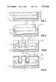
- FIGS. 1-6illustrate steps in the process of fabricating a heterojunction bipolar transistor (HBT) according to the invention.
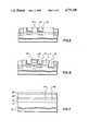
- FIG. 7illustrates a double heterojunction bipolar semiconductor wafer suitable for fabricating a HBT according to the invention.
- FIG. 1shows a heterojunction bipolar semiconductor wafer suitable for forming a heterojunction bipolar transistor (HBT).
- HBTheterojunction bipolar transistor
- MBEmolecular beam epitaxy
- MOCVDmetal organic chemical vapor deposition
- the wafer in FIG. 1has a single heterojunction 6 formed between two different semiconductor compounds, AlGaAs 2 and GaAs 4. Because the AlGaAs semiconductor has n-type conductivity 8 and the adjacent GaAs has p-type conductivity 10, heterojunction 6 is also a p-n junction. A second p-n junction 14 is formed below heterojunction 6 by appropriate doping of GaAs semiconductor 4.
- FIG. 1also shows a cap layer 1 which is formed on top of the wafer to facilitate making ohmic contact to an emitter.
- Cap 1is a thin layer of an n + -type conductivity material such as GaAs or InAs as is known in the prior art.
- a photoresist mask 16is formed on cap layer 1 and an isolation implant 18 made around the transistor location. Additionally, cap layer 1 is etched to provide a mesa in the transistor location.
- photoresist 16is removed and a second photoresist mask 20 is formed on the wafer. Openings in mask 20 define an emitter location 19, and semiconductor 2 is etched through these openings down to heterojunction 6 to define base location 21.
- Protons 22can be implanted through the openings into semiconductor 4 below the base location. This implanted area 24 reduces the HBT's extrinsic base-collector capacitance. Its location and depth is determined by the energy used to implant the protons.
- the term protonsis used to include sources such as He, B, and O 2 .
- the proton implantationis a self-aligned step because photoresist mask 20 is used rather than requiring an additional, separately aligned mask.
- base contact metal 26is then deposited on photoresist mask 20 and on exposed base location 21 to form base contact 30.
- Base contact metal 26is then covered with a dielectric 28 such as photo-enhanced chemically vapor deposited SiO 2 .
- the photoresistcan be etched back somewhat using an O 2 plasma. Formation of base contact 30 and covering it with dielectric 26 are also self-aligned steps because an additional mask and alignment are not required.
- Photoresist mask 20 with its overlying deposits of contact metal 26 and dielectric 28are lifted off the wafer. This dual lift-off step leaves dielectric 28 covering base contact 30 and the adjacent sidewalls. It also leaves an exposed emitter contact location 32 as shown in FIG. 5.
- the emitter contact metalis defined by another photoresist mask, and emitter contact metal 34 is deposited. Although this step requires alignment of a new mask, the alignment is not as critical as required in prior art processes. Greater alignment tolerance is acceptable because contact 30 is covered with dielectric 26. As shown in FIG. 6, emitter contact metal 34 can overlap the extrinsic base location or base contact 30 without concern for emitter-base shorting because of the dielectric coverage. Such overlap, if it occurs, would produce only a slight increase in fringing capacitance.
- collector contact locationFor the example shown in FIG. 6, a mask is provided to define a collector contact location, and the wafer is etched down to the n-type conductivity region 12 of the GaAs semiconductor compound 4.
- Collector contact metal 36is then deposited through the opening and onto the collector contact location.
- the alignment required to define the contact location and deposit the contact metalis not critical (at least when compared to the emitter and base alignment), and consequently collector contact 36 can be provided without degrading the HBT's performance.
- Interconnections of the three transistor contacts with other devices on the wafercan be accomplished using conventional masking, etching and metal deposition techniques.
- a double heterojunction bipolar transistoris fabricated using the method of the invention.
- the starting waferis a double heterojunction structure such as shown in FIG. 7 rather than the single heterostructure wafer shown in FIG. 6.
- a layer 44 of n-type conductivity AlGaAsis formed on a suitable GaAs substrate 46 using known growth techniques such as MBE or MOCVD.
- a layer 42 of p-type conductivity GaAsis grown on the AlGaAs layer 44, thus creating hetero-p-n junction 56.
- Another layer 40 of n-type conductivity AlGaAsis grown on GaAs layer 42 to create the second hetero-p-n junction 54.
- cap layer 38is formed on top of the wafer to facilitate making ohmic contact.
- the emitter base and collector contactsare then formed on appropriate p and n-type material as previously described for the single HBT.
- the composition of the semiconductorscan be graded to provide improved lattice match and conductivity.
- Other Group III-V semiconductor compoundssuch as InP can be used.
- p-n-p bipolar transistors in addition to the exemplary n-p-n bipolar transistorscan be fabricated using appropriate dopants.
- the methodcan be applied using dual or multiple layer photoresist processes to facilitate liftoff. Accordingly, it should be understood that the form of the invention described above is illustrative and is not intended to limit the scope of the invention.
Landscapes
- Engineering & Computer Science (AREA)
- Physics & Mathematics (AREA)
- Condensed Matter Physics & Semiconductors (AREA)
- General Physics & Mathematics (AREA)
- Manufacturing & Machinery (AREA)
- Computer Hardware Design (AREA)
- Microelectronics & Electronic Packaging (AREA)
- Power Engineering (AREA)
- Bipolar Transistors (AREA)
Abstract
Description
Claims (18)
Priority Applications (1)
| Application Number | Priority Date | Filing Date | Title |
|---|---|---|---|
| US07/017,957US4731340A (en) | 1987-02-24 | 1987-02-24 | Dual lift-off self aligning process for making heterojunction bipolar transistors |
Applications Claiming Priority (1)
| Application Number | Priority Date | Filing Date | Title |
|---|---|---|---|
| US07/017,957US4731340A (en) | 1987-02-24 | 1987-02-24 | Dual lift-off self aligning process for making heterojunction bipolar transistors |
Publications (1)
| Publication Number | Publication Date |
|---|---|
| US4731340Atrue US4731340A (en) | 1988-03-15 |
Family
ID=21785486
Family Applications (1)
| Application Number | Title | Priority Date | Filing Date |
|---|---|---|---|
| US07/017,957Expired - LifetimeUS4731340A (en) | 1987-02-24 | 1987-02-24 | Dual lift-off self aligning process for making heterojunction bipolar transistors |
Country Status (1)
| Country | Link |
|---|---|
| US (1) | US4731340A (en) |
Cited By (27)
| Publication number | Priority date | Publication date | Assignee | Title |
|---|---|---|---|---|
| US4839303A (en)* | 1987-10-13 | 1989-06-13 | Northrop Corporation | Planar bipolar transistors including heterojunction transistors and method |
| US4904612A (en)* | 1987-10-23 | 1990-02-27 | Siemens Aktiengesellschaft | Method for manufacturing a planar, self-aligned emitter-base complex |
| US4914049A (en)* | 1989-10-16 | 1990-04-03 | Motorola, Inc. | Method of fabricating a heterojunction bipolar transistor |
| EP0367698A3 (en)* | 1988-10-31 | 1990-07-11 | International Business Machines Corporation | Heretojunction bipolar transistor |
| US4954457A (en)* | 1988-10-31 | 1990-09-04 | International Business Machines Corporation | Method of making heterojunction bipolar transistors |
| US4981808A (en)* | 1986-03-27 | 1991-01-01 | Plessey Overseas Limited | Process for the manufacture of III-V semiconductor devices |
| US4996165A (en)* | 1989-04-21 | 1991-02-26 | Rockwell International Corporation | Self-aligned dielectric assisted planarization process |
| US5019519A (en)* | 1988-03-11 | 1991-05-28 | Kokusai Denshin Denwa Kabushiki Kaisha | Method for the manufacture of optical semiconductor device |
| US5028549A (en)* | 1989-04-10 | 1991-07-02 | Rockwell International | Etched back edge isolation process for heterojunction bipolar transistors |
| US5064772A (en)* | 1988-08-31 | 1991-11-12 | International Business Machines Corporation | Bipolar transistor integrated circuit technology |
| US5185274A (en)* | 1991-08-15 | 1993-02-09 | Rockwell International Corporation | Self-aligned, self-passivated advanced dual lift-off heterojunction bipolar transistor method |
| US5254483A (en)* | 1987-10-23 | 1993-10-19 | Vitesse Semiconductor Corporation | Gate-to-ohmic metal contact scheme for III-V devices |
| US5272095A (en)* | 1992-03-18 | 1993-12-21 | Research Triangle Institute | Method of manufacturing heterojunction transistors with self-aligned metal contacts |
| US5468659A (en)* | 1994-03-10 | 1995-11-21 | Hughes Aircraft Company | Reduction of base-collector junction parasitic capacitance of heterojunction bipolar transistors |
| US5525817A (en)* | 1992-10-16 | 1996-06-11 | Texas Instruments Incorporated | Bipolar transistor |
| US5773333A (en)* | 1995-12-30 | 1998-06-30 | Lg Semicon Co., Ltd. | Method for manufacturing self-aligned T-type gate |
| US5840612A (en)* | 1996-05-13 | 1998-11-24 | Trw Inc. | Method of fabricating very high gain heterojunction bipolar transistors |
| US5882995A (en)* | 1996-03-26 | 1999-03-16 | Sharp Kabushiki Kaisha | Method of forming ohmic electrodes on semiconductor wafer |
| US6576937B2 (en)* | 2000-06-01 | 2003-06-10 | Hitachi, Ltd. | Semiconductor device and power amplifier using the same |
| US20050254994A1 (en)* | 2002-04-01 | 2005-11-17 | Palo Alto Research Center Incorporated | Thermal sensing with bridge circuitry |
| US20050265898A1 (en)* | 2002-04-01 | 2005-12-01 | Palo Alto Research Center Incorporated | Thermal sensing |
| US20060078999A1 (en)* | 2002-04-01 | 2006-04-13 | Palo Alto Research Center Incorporated | Apparatus and method for a nanocalorimeter for detecting chemical reactions |
| US20070147473A1 (en)* | 2005-12-27 | 2007-06-28 | Palo Alto Research Center Incorporated | Producing layered structures using printing |
| US20070148416A1 (en)* | 2005-12-27 | 2007-06-28 | Palo Alto Research Center Incorporated | Layered structures on thin substrates |
| US20070145362A1 (en)* | 2005-12-27 | 2007-06-28 | Palo Alto Research Center Incorporated | Passive electronic devices |
| DE102015102374A1 (en)* | 2015-02-19 | 2016-08-25 | Osram Opto Semiconductors Gmbh | Method for producing a semiconductor body |
| DE102015102378A1 (en)* | 2015-02-19 | 2016-08-25 | Osram Opto Semiconductors Gmbh | Method for producing a semiconductor body |
Citations (4)
| Publication number | Priority date | Publication date | Assignee | Title |
|---|---|---|---|---|
| US4090006A (en)* | 1976-04-29 | 1978-05-16 | International Business Machines Corporation | Structure for making coplanar layers of thin films |
| US4380774A (en)* | 1980-12-19 | 1983-04-19 | The United States Of America As Represented By The Secretary Of The Navy | High-performance bipolar microwave transistor |
| US4448800A (en)* | 1981-08-10 | 1984-05-15 | Nippon Telegraph And Telephone Public Corporation | Method for the manufacture of semiconductor device using refractory metal in a lift-off step |
| EP0177246A1 (en)* | 1984-09-29 | 1986-04-09 | Kabushiki Kaisha Toshiba | Heterojunction bipolar transistor and method of manufacturing the same |
- 1987
- 1987-02-24USUS07/017,957patent/US4731340A/ennot_activeExpired - Lifetime
Patent Citations (4)
| Publication number | Priority date | Publication date | Assignee | Title |
|---|---|---|---|---|
| US4090006A (en)* | 1976-04-29 | 1978-05-16 | International Business Machines Corporation | Structure for making coplanar layers of thin films |
| US4380774A (en)* | 1980-12-19 | 1983-04-19 | The United States Of America As Represented By The Secretary Of The Navy | High-performance bipolar microwave transistor |
| US4448800A (en)* | 1981-08-10 | 1984-05-15 | Nippon Telegraph And Telephone Public Corporation | Method for the manufacture of semiconductor device using refractory metal in a lift-off step |
| EP0177246A1 (en)* | 1984-09-29 | 1986-04-09 | Kabushiki Kaisha Toshiba | Heterojunction bipolar transistor and method of manufacturing the same |
Non-Patent Citations (2)
| Title |
|---|
| Kroemer, H. "Heterostructure Bipolar . . ." Proceedings of the IEEE vol. 70, #1, Jan. 1982, pp. 13-25. |
| Kroemer, H. Heterostructure Bipolar . . . Proceedings of the IEEE vol. 70, 1, Jan. 1982, pp. 13 25.* |
Cited By (40)
| Publication number | Priority date | Publication date | Assignee | Title |
|---|---|---|---|---|
| US4981808A (en)* | 1986-03-27 | 1991-01-01 | Plessey Overseas Limited | Process for the manufacture of III-V semiconductor devices |
| US4839303A (en)* | 1987-10-13 | 1989-06-13 | Northrop Corporation | Planar bipolar transistors including heterojunction transistors and method |
| US5254483A (en)* | 1987-10-23 | 1993-10-19 | Vitesse Semiconductor Corporation | Gate-to-ohmic metal contact scheme for III-V devices |
| US4904612A (en)* | 1987-10-23 | 1990-02-27 | Siemens Aktiengesellschaft | Method for manufacturing a planar, self-aligned emitter-base complex |
| US5019519A (en)* | 1988-03-11 | 1991-05-28 | Kokusai Denshin Denwa Kabushiki Kaisha | Method for the manufacture of optical semiconductor device |
| US5064772A (en)* | 1988-08-31 | 1991-11-12 | International Business Machines Corporation | Bipolar transistor integrated circuit technology |
| EP0367698A3 (en)* | 1988-10-31 | 1990-07-11 | International Business Machines Corporation | Heretojunction bipolar transistor |
| US4954457A (en)* | 1988-10-31 | 1990-09-04 | International Business Machines Corporation | Method of making heterojunction bipolar transistors |
| US5028549A (en)* | 1989-04-10 | 1991-07-02 | Rockwell International | Etched back edge isolation process for heterojunction bipolar transistors |
| US4996165A (en)* | 1989-04-21 | 1991-02-26 | Rockwell International Corporation | Self-aligned dielectric assisted planarization process |
| US4914049A (en)* | 1989-10-16 | 1990-04-03 | Motorola, Inc. | Method of fabricating a heterojunction bipolar transistor |
| US5185274A (en)* | 1991-08-15 | 1993-02-09 | Rockwell International Corporation | Self-aligned, self-passivated advanced dual lift-off heterojunction bipolar transistor method |
| US5272095A (en)* | 1992-03-18 | 1993-12-21 | Research Triangle Institute | Method of manufacturing heterojunction transistors with self-aligned metal contacts |
| US5525817A (en)* | 1992-10-16 | 1996-06-11 | Texas Instruments Incorporated | Bipolar transistor |
| US5468659A (en)* | 1994-03-10 | 1995-11-21 | Hughes Aircraft Company | Reduction of base-collector junction parasitic capacitance of heterojunction bipolar transistors |
| US5773333A (en)* | 1995-12-30 | 1998-06-30 | Lg Semicon Co., Ltd. | Method for manufacturing self-aligned T-type gate |
| US5882995A (en)* | 1996-03-26 | 1999-03-16 | Sharp Kabushiki Kaisha | Method of forming ohmic electrodes on semiconductor wafer |
| US5840612A (en)* | 1996-05-13 | 1998-11-24 | Trw Inc. | Method of fabricating very high gain heterojunction bipolar transistors |
| US6576937B2 (en)* | 2000-06-01 | 2003-06-10 | Hitachi, Ltd. | Semiconductor device and power amplifier using the same |
| US6724020B2 (en) | 2000-06-01 | 2004-04-20 | Renesas Technology Corporation | Semiconductor device and power amplifier using the same |
| US20050254994A1 (en)* | 2002-04-01 | 2005-11-17 | Palo Alto Research Center Incorporated | Thermal sensing with bridge circuitry |
| US7727768B2 (en) | 2002-04-01 | 2010-06-01 | Palo Alto Research Center Incorporated | Method for a nanocalorimeter for detecting chemical reactions |
| US20060078999A1 (en)* | 2002-04-01 | 2006-04-13 | Palo Alto Research Center Incorporated | Apparatus and method for a nanocalorimeter for detecting chemical reactions |
| US7833800B2 (en) | 2002-04-01 | 2010-11-16 | Palo Alto Research Center Incorporated | Thermal sensing with bridge circuitry |
| US20050265898A1 (en)* | 2002-04-01 | 2005-12-01 | Palo Alto Research Center Incorporated | Thermal sensing |
| US7754492B2 (en) | 2002-04-01 | 2010-07-13 | Palo Alto Research Center Incorporated | Thermal sensing device |
| US7816146B2 (en) | 2005-12-27 | 2010-10-19 | Palo Alto Research Center Incorporated | Passive electronic devices |
| US10046584B2 (en) | 2005-12-27 | 2018-08-14 | Palo Alto Research Center Incorporated | Layered structures on thin substrates |
| US7784173B2 (en)* | 2005-12-27 | 2010-08-31 | Palo Alto Research Center Incorporated | Producing layered structures using printing |
| US20070148416A1 (en)* | 2005-12-27 | 2007-06-28 | Palo Alto Research Center Incorporated | Layered structures on thin substrates |
| US20070147473A1 (en)* | 2005-12-27 | 2007-06-28 | Palo Alto Research Center Incorporated | Producing layered structures using printing |
| US8637138B2 (en) | 2005-12-27 | 2014-01-28 | Palo Alto Research Center Incorporated | Layered structures on thin substrates |
| US20070145362A1 (en)* | 2005-12-27 | 2007-06-28 | Palo Alto Research Center Incorporated | Passive electronic devices |
| US9528888B2 (en) | 2005-12-27 | 2016-12-27 | Palo Alto Research Center Incorporated | Method for producing layered structures on thin substrates |
| DE102015102378A1 (en)* | 2015-02-19 | 2016-08-25 | Osram Opto Semiconductors Gmbh | Method for producing a semiconductor body |
| CN107251238A (en)* | 2015-02-19 | 2017-10-13 | 欧司朗光电半导体有限公司 | Method for manufacturing semiconductor body |
| DE102015102374A1 (en)* | 2015-02-19 | 2016-08-25 | Osram Opto Semiconductors Gmbh | Method for producing a semiconductor body |
| US10424509B2 (en) | 2015-02-19 | 2019-09-24 | Osram Opto Semiconductors Gmbh | Method for producing a semiconductor body |
| US10468555B2 (en) | 2015-02-19 | 2019-11-05 | Osram Opto Semiconductors Gmbh | Method for producing a semiconductor body |
| DE102015102378B4 (en) | 2015-02-19 | 2022-09-15 | OSRAM Opto Semiconductors Gesellschaft mit beschränkter Haftung | Process for producing a semiconductor body |
Similar Documents
| Publication | Publication Date | Title |
|---|---|---|
| US4731340A (en) | Dual lift-off self aligning process for making heterojunction bipolar transistors | |
| US5407842A (en) | Enhanced performance bipolar transistor process | |
| US4965650A (en) | Bipolar transistor and method of producing the same | |
| US4683487A (en) | Heterojunction bipolar transistor | |
| US4593457A (en) | Method for making gallium arsenide NPN transistor with self-aligned base enhancement to emitter region and metal contact | |
| US8697532B2 (en) | InP based heterojunction bipolar transistors with emitter-up and emitter-down profiles on a common wafer | |
| US4751195A (en) | Method of manufacturing a heterojunction bipolar transistor | |
| US5298439A (en) | 1/f noise reduction in heterojunction bipolar transistors | |
| US5324671A (en) | Method of fabrication an integrated circuit including bipolar and field effect devices | |
| US5344786A (en) | Method of fabricating self-aligned heterojunction bipolar transistors | |
| US5064772A (en) | Bipolar transistor integrated circuit technology | |
| US4839303A (en) | Planar bipolar transistors including heterojunction transistors and method | |
| JPH084091B2 (en) | Planar heterojunction bipolar device and fabrication method thereof | |
| US5098853A (en) | Self-aligned, planar heterojunction bipolar transistor and method of forming the same | |
| US4967254A (en) | Semiconductor device | |
| US5648666A (en) | Double-epitaxy heterojunction bipolar transistors for high speed performance | |
| US5242843A (en) | Method for making a heterojunction bipolar transistor with improved high frequency response | |
| US5093272A (en) | Manufacturing method for a self-aligned emitter-base-complex for heterobipolar transistors | |
| US4967253A (en) | Bipolar transistor integrated circuit technology | |
| US5471078A (en) | Self-aligned heterojunction bipolar transistor | |
| US5070028A (en) | Method for manufacturing bipolar transistors having extremely reduced base-collection capacitance | |
| US5153692A (en) | Semiconductor device | |
| JPH11251328A (en) | Compound semiconductor device | |
| US5028549A (en) | Etched back edge isolation process for heterojunction bipolar transistors | |
| KR100275496B1 (en) | Method for fabricating the heterojunction bipolar transistor |
Legal Events
| Date | Code | Title | Description |
|---|---|---|---|
| AS | Assignment | Owner name:ROCKWELL INTERNATIONAL CORPORATION Free format text:ASSIGNMENT OF ASSIGNORS INTEREST.;ASSIGNORS:CHANG, MAU-CHUNG F.;ASBECK, PETER M.;REEL/FRAME:004695/0075 Effective date:19870217 | |
| STCF | Information on status: patent grant | Free format text:PATENTED CASE | |
| FPAY | Fee payment | Year of fee payment:4 | |
| FPAY | Fee payment | Year of fee payment:8 | |
| AS | Assignment | Owner name:CREDIT SUISSE FIRST BOSTON, NEW YORK Free format text:SECURITY INTEREST;ASSIGNORS:CONEXANT SYSTEMS, INC.;BROOKTREE CORPORATION;BROOKTREE WORLDWIDE SALES CORPORATION;AND OTHERS;REEL/FRAME:009719/0537 Effective date:19981221 | |
| FPAY | Fee payment | Year of fee payment:12 | |
| AS | Assignment | Owner name:CONEXANT SYSTEMS, INC., CALIFORNIA Free format text:ASSIGNMENT OF ASSIGNORS INTEREST;ASSIGNOR:ROCKWELL SCIENCE CENTER, LLC;REEL/FRAME:010415/0761 Effective date:19981210 | |
| AS | Assignment | Owner name:CONEXANT SYSTEMS, INC., CALIFORNIA Free format text:RELEASE OF SECURITY INTEREST;ASSIGNOR:CREDIT SUISSE FIRST BOSTON;REEL/FRAME:012252/0413 Effective date:20011018 Owner name:BROOKTREE CORPORATION, CALIFORNIA Free format text:RELEASE OF SECURITY INTEREST;ASSIGNOR:CREDIT SUISSE FIRST BOSTON;REEL/FRAME:012252/0413 Effective date:20011018 Owner name:BROOKTREE WORLDWIDE SALES CORPORATION, CALIFORNIA Free format text:RELEASE OF SECURITY INTEREST;ASSIGNOR:CREDIT SUISSE FIRST BOSTON;REEL/FRAME:012252/0413 Effective date:20011018 Owner name:CONEXANT SYSTEMS WORLDWIDE, INC., CALIFORNIA Free format text:RELEASE OF SECURITY INTEREST;ASSIGNOR:CREDIT SUISSE FIRST BOSTON;REEL/FRAME:012252/0413 Effective date:20011018 | |
| AS | Assignment | Owner name:TELEDYNE SCIENTIFIC & IMAGING, LLC, CALIFORNIA Free format text:CHANGE OF NAME;ASSIGNOR:ROCKWELL SCIENTIFIC COMPANY, LLC;REEL/FRAME:018855/0939 Effective date:20060918 Owner name:ROCKWELL SCIENTIFIC COMPANY, LLC, CALIFORNIA Free format text:ASSIGNMENT OF ASSIGNORS INTEREST;ASSIGNOR:CONEXANT SYSTEMS, INC.;REEL/FRAME:018855/0931 Effective date:20011031 |