US4727424A - Sampled data filtering system, including a crossbar switch matrix, as for a ghost cancellation system - Google Patents
Sampled data filtering system, including a crossbar switch matrix, as for a ghost cancellation systemDownload PDFInfo
- Publication number
- US4727424A US4727424AUS06/919,494US91949486AUS4727424AUS 4727424 AUS4727424 AUS 4727424AUS 91949486 AUS91949486 AUS 91949486AUS 4727424 AUS4727424 AUS 4727424A
- Authority
- US
- United States
- Prior art keywords
- coupled
- signal
- sampled data
- matrix
- sample
- Prior art date
- Legal status (The legal status is an assumption and is not a legal conclusion. Google has not performed a legal analysis and makes no representation as to the accuracy of the status listed.)
- Expired - Fee Related
Links
Images


Classifications
- H—ELECTRICITY
- H03—ELECTRONIC CIRCUITRY
- H03H—IMPEDANCE NETWORKS, e.g. RESONANT CIRCUITS; RESONATORS
- H03H15/00—Transversal filters
- H03H15/02—Transversal filters using analogue shift registers
- H—ELECTRICITY
- H04—ELECTRIC COMMUNICATION TECHNIQUE
- H04N—PICTORIAL COMMUNICATION, e.g. TELEVISION
- H04N5/00—Details of television systems
- H04N5/14—Picture signal circuitry for video frequency region
- H04N5/21—Circuitry for suppressing or minimising disturbance, e.g. moiré or halo
- H04N5/211—Ghost signal cancellation
Definitions
- the present inventionconcerns a multi-tap sampled data filtering system which uses a crossbar switch matrix to provide programmable tap delays.
- a sampled data signalis delayed, either through a chain of delay elements having interstitial taps or through multiple parallel delay elements. Delayed signals, taken at selected tap positions or at the output ports of the multiple delay elements, are multiplied by respective filter coefficient values and then added together by summing circuitry.
- FIR filterthe input signal to the filtering system is the signal that is applied to the delay elements, and the output signal is provided by the summing circuitry.
- IIRthe input signal is added to the signal provided by the summing circuitry to produce the signal that is applied to the delay elements. This signal is also the output signal of the filter.
- a filter of this typemay be used, for example, in a system for reducing multipath distortion such as an automatic ghost cancellation system in a television receiver.
- a first type of ghost cancellation filterthe video signal, contaminated by multipath or ghost signals, is delayed by successive stages of a fixed delay line, such as a charge transfer delay device (CTD).
- CTDcharge transfer delay device
- the respective delayed signalsare extracted, weighted by filter coefficient values and combined to form a psuedo-ghost signal suitable for canceling the ghost component of the contaminated video signal.
- this type of filterthere is a tap for every delay element and a filter coefficient multiplier for every tap. However, not all taps contribute to the filtered output signal, only those having non-zero filter coefficient values.
- a ghost cancellation filter of this typeis described, for example, in U.S. Pat. No. 4,344,089 entitled "Ghost Cancelling System", which is hereby incorporated by reference.
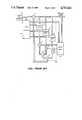
- a second type of filtering systemis shown in the automatic ghost cancellation system of FIG. 1.
- contaminated video signals provided by a source 5are applied to an IIR filter, which includes an adder 12 and an FIR filter 40.
- the IIR filteris responsive to the contaminated video signal to develop a psuedo-ghost signal having a polarity which is opposite to that of the contaminating ghost signal. This psuedo-ghost signal is added to the contaminated signal in the adder 12 to substantially cancel the ghost signal component of the video signal.
- up to three ghost signals in the input video signalsare detected by a ghost detector 10.
- the detector 10sets the amount of time delay provided by each of three variable delay elements 14, 16 and 18 to develop the psuedo-ghost signals for the three detected ghost signals, respectively.
- the ghost detector 10also provides a signal to the filter coefficient generating circuitry 20 which, using this signal and the output signal of the adder 12, develops filter coefficient values for three multipliers 22, 24 and 26 coupled to the output ports of the delay elements 14, 16 and 18, respectively.
- the multipliersappropriately scale and reverse the polarity of the delayed main signal to develop the psuedo-ghost signals.
- the three psuedo-ghost signalsare combined by the adders 28 and 30 to develop the signal which, when applied to the adder 12, cancels the three ghost signals from the input video signals.
- a ghost signal cancellation system similar to that shown in FIG. 1is described in U.S. Pat. No. 4,542,408 entitled “Digital Deghosting System", which is hereby incorporated by reference.
- the sampled data signal provided by the adder 12is delayed by the three parallel delay elements 14, 16 and 18, the output ports of which may be considered to be the taps of a delay line.
- the amount of time delay provided by each of the delay elementsis variable, thus, the position of each tap on the delay line is variable.
- each of the delay elements 14, 16 and 18should have sufficient memory to allow its associated tap to provide the longest possible time delay.
- this systemuses three times the memory of the first described system. Even though it uses more memory, this filter configuration is preferred over the first described system for digital ghost cancellation systems because it uses a small number of multipliers, which are relatively complex digital devices.
- the present inventionis embodied in a sampled data signal filtering system.
- the systemincludes N serially connected delay elements and M sample scaling circuits, where N and M are both integers and M is less than N.
- a multi-port controllable switching networkis configured to couple the output terminals of selected ones of the delay elements to input ports of respectively different ones of the sample scaling circuits.
- FIG. 1(prior art) is a block diagram of a ghost cancellation system useful for explaining an environment for using the present invention.
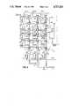
- FIG. 2is a block diagram of a portion of a sampled data filter embodying the present invention.
- FIGS. 3 and 4are block diagrams, partially in schematic diagram form, of alternate switching networks which may be used in the sampled data filter shown in FIG. 2.
- broad arrowsrepresent signal paths, i.e. connections for conveying analog signals or busses for conveying multiple-bit parallel digital signals.
- Line arrowsrepresent connections for conveying analog signals or single bit digital signals.
- compensating delaysmay be required in certain of the signal paths and connections.
- One skilled in the art of digital signal processing circuit designwill know where such delays are needed in a particular system.
- FIG. 2is a block diagram of circuitry which may be used in place of the FIR filter 40 shown in FIG. 1.
- the filter shown in FIG. 2uses a single chain of delay elements ⁇ 0 , ⁇ 1 , . . . ⁇ 383 and a crossbar switch 200 to realize the same function as the three programmable delay elements 14, 16 and 18, of the system shown in FIG. 1.
- Each of the delay elements, ⁇ 0 through ⁇ 383delays the samples applied to its input port by a fixed amount of time, for example, one period of the sampling clock signal.
- the samples applied to the input port of the filter and the samples available at the output port of each of the delay elements ⁇ 0 through ⁇ 383are applied to respectively different input ports of the crossbar switch matrix 200.
- the samples provided by selected ones of the delay elementsare applied to the input terminals of the multipliers 212, 214 and 216 by respectively selected switches in each of the columns of switch elements; SA0 through SA384, SB0 through SB384 and SC0 through SC384.
- An individual switch elementis selected to couple its input samples to its associated output port by one of the signals SEL0 through SEL384, generated by the row select circuitry 210, and by one of the column select signals, C0LA, C0LB and C0LC.
- the row select circuitry 210may, for example, be the same as the address decoding circuitry used in a conventional 512 by 1 bit random access memory (RAM).
- the circuitry 210activates one of the signals SEL0 through SEL384.
- one of the column select signals, C0LA, C0LB or C0LC, also provided by the ghost detector 10is pulsed to close the selected switch element.
- FIG. 3is a block diagram of a switch element suitable for use in a parallel-bit digital embodiment of the present invention.
- the output signal path of an arbitrary delay element, ⁇ xis shown as eight one-bit connections DX 0 through DX 7 and the output data path of the switch element is shown as eight one-bit connections MX 0 through MX 7 .
- Each of the input signal pathsis coupled to a corresponding output signal path by an enhancement mode field effect transistor (FET) configured as a transmission gate.
- FETenhancement mode field effect transistor
- the source electrodes of the transistors Q 0 through Q 7are connected to the respective input connections DX 0 through DX 7
- the drain electrodes of the transistors Q 0 through Q 7are connected to respective output connections MX 0 through MX 7 .
- the gate electrodes of the transistors Q 0 through Q 7are connected together.
- the interconnected gate electrodes of the transistors Q 0 through Q 7are connected to the output terminal, Q, of a flip-flop 310.
- the data (D) and clock (CLK) input terminals of the flip-flop 310are coupled to receive the respective row select signal (SELX) and column select signal (COLX) applied to the switch element. If the signal SELX is a logic zero when the signal COLX is strobed, the signal available at the Q output terminal is a logic zero, the transistors Q 0 through Q 7 are turned off and the input signal paths DX 0 through DX 7 are not connected to the output signal paths MX 0 through MX 7 .
- the switch elementschange state one column at a time as each of the three column select signals is strobed. Consequently, while the filter system is changing from its current transfer function to a new transfer function, it may pass through intermediate states in which it exhibits undesirable transfer functions.
- a second flip-flop 312(shown in phantom) may be included in the circuitry for each switching element, in place of the connection A.
- the flip-flops 310 and 312are in a master-slave relationship. While the new filter state is being stored in the flip-flop 310, as described above, the flip-flop 312 keeps the system operating in the old state.
- a clock pulse CKFis simultaneously applied to all of the flip-flops 312, changing the state of the filter to implement the new transfer function.
- the separate row select connections SEL0 through SEL384may be eliminated by configuring the flip-flops 310 of each column of switch elements as a shift register.
- the row select circuitry 210may, for example, include a shift register (not shown) having a number of stages equal to the number of rows of switch elements in the crossbar switch matrix. This shift register may be connected, via a multiplexer, (not shown) to the three column shift registers formed by the interconnected flip-flops 310.
- the shift register stage or sample delay element to be connected to the multiplier input terminalis selected by the row select circuitry and which stores a logic one at the corresponding location in its internal shift register and logic zeroes at all other locations.
- This shift registeris then clocked by the appropriate column select signal to transfer the selected switch states to the corresponding row locations in the appropriate column shift register.
- a pulse applied to the CKF input terminal of the flip-flop 312then reconfigures the switch elements to change the transfer function of the filter.
- the interconnection of the flip-flops 310 as a shift registeris shown by the phantom signal SELSH which is applied to the D input terminal of the flip-flop 310 and propogated to the flip-flop 310 of the next sequential switch element, as the signal SELSH', via the Q output terminal of the flip-flop 310.
- FIG. 4illustrates an alternative switch element circuit which may be used when the delay elements ⁇ 0 through ⁇ 383 are realized using a CTD.
- a signal, DX, generated from the charge provided at a tap of the CTDis applied to the interconnected drain and source electrodes of two complementary FET's 402 and 404 respectively.
- the interconnected source and drain electrodes of the transistors 402 and 404are connected to the output signal path MX.
- the gate electrodes of the complementary FET's 402 and 404are connected to the respective Q and Q output terminals of a flip-flop 410.
- the FET's 402 and 404are conditioned to conduct when the signals provided by the terminals Q and Q are logic one and logic zero, respectively, and conditioned to be non-conducting when the signals at the terminals Q and Q are logic zero and logic one, respectively.
- the row select signal SELX and column select signal COLXare applied to the respective D and CLK input terminals of the flip-flop 410.
- the row select signal SELXis developed by the row select circuitry 210 and applied to the switch element. This row select signal is stored into the flip-flop 410 when the column select signal, COLX, is strobed.
- the signal SELXis a logic zero
- the signals at the Q and Q output terminals of the flip-flop 410are logic zero and logic one respectively and both transistors are turned off so the signal path DX is not connected to the signal path MX.
- the signals at the Q and Q output terminals of the flip-flop 410are logic one and logic zero signals, respectively, and the signal path DX is connected to the signal path MX.
- the switch configuration shown in FIG. 4is preferred when analog signals are to be switched since the parallel arrangement of the complementary transistors 402 and 404 allows analog signals to be switched with only insignificant distortion, even when the output data path provides a significant capacitive load.
- the alternative embodiment of the switch element, described in reference to FIG. 3, involving the flip-flop 312 and the configuration of the flip-flop 310 as one stage in a shift registermay be used with the switch element shown in FIG. 4.
- the single FET transmission gates Q 0 through Q 7 shown in FIG. 3may be replaced by complementary FET transmission gates identical to the one shown in FIG. 4, or by any other circuitry which realizes a transmission gate function.
- the signals conveyed by the signal paths MA, MB and MCare multiplied by coefficients, stored in latches 218, 220 and 222, by the respective multipliers 212, 214 and 216.
- the output signals produced by the multipliers 212 and 214are summed by an adder 224, the output signal of which is summed with the output signal of the multiplier 216 in the adder 226.
- the signal provided by the adder 226is the output signal of the FIR filter.
- the filter coefficient valuesare applied to the latches 218, 220 and 222 via the input signal path COEFF.
- a coefficient value for a particular column multiplieris applied to the latch input terminals at the same time that row address value for the column is applied to the row select circuitry 210.
- the coefficient valueis loaded into the latch at the same time that the switch state for the column is set.
- the latches 218, 220 and 222would be sample-and-hold circuits and the signal path COEFF would provide analog coefficient values.
- this inventionmay be practiced in the context of an input weighted sampled data filter.
- an input weighted filterthe individual delay elements are separated by signal summing circuitry.
- Input sample valuesare first weighted by the filter coefficient values and then applied to the input terminals of the summing circuits coupled to selected ones of the cascaded delay elements. At each of the selected delay elements, the weighted samples are summed with the values propogating through the preceding delay elements.
- the present inventionwould be realized in this context by placing the crossbar switch between the output terminals of the weighting circuits and the input terminals of the summing circuits between the cascaded delay elements.
- a complex filtereither input weighted or output weighted, may be implemented using similar techniques.
- a complex filter built in accordance with the present inventionwould have two parallel chains of delay elements, one for the real signal and one for the imaginary signal.
- each of the switch elementswould couple the samples provided by corresponding stages of the two delay lines to real and imaginary output signal paths.
- the output signal pathswould be connected to complex multipliers which would multiply the real and imaginary signals by real and imaginary coefficient values to produce real and imaginary output values.
- the real and imaginary signals provided by the complex multiplierswould be summed separately to provide the real and imaginary components of the complex output signal.
Landscapes
- Engineering & Computer Science (AREA)
- Multimedia (AREA)
- Signal Processing (AREA)
- Filters That Use Time-Delay Elements (AREA)
Abstract
Description
The present invention concerns a multi-tap sampled data filtering system which uses a crossbar switch matrix to provide programmable tap delays.
In finite impulse response (FIR) and infinite impulse response (IIR) sampled data filtering systems, a sampled data signal is delayed, either through a chain of delay elements having interstitial taps or through multiple parallel delay elements. Delayed signals, taken at selected tap positions or at the output ports of the multiple delay elements, are multiplied by respective filter coefficient values and then added together by summing circuitry. In an FIR filter, the input signal to the filtering system is the signal that is applied to the delay elements, and the output signal is provided by the summing circuitry. In an IIR system, the input signal is added to the signal provided by the summing circuitry to produce the signal that is applied to the delay elements. This signal is also the output signal of the filter.
One type of filtering system has been difficult to implement economically as a sampled data filtering system. This type of filter is best visualized as a relatively long chain of delay elements having a relatively small number of taps which may have variable locations along the chain. A filter of this type may be used, for example, in a system for reducing multipath distortion such as an automatic ghost cancellation system in a television receiver.
In a first type of ghost cancellation filter, the video signal, contaminated by multipath or ghost signals, is delayed by successive stages of a fixed delay line, such as a charge transfer delay device (CTD). At the outputs of the delay line stages, the respective delayed signals are extracted, weighted by filter coefficient values and combined to form a psuedo-ghost signal suitable for canceling the ghost component of the contaminated video signal. In this type of filter there is a tap for every delay element and a filter coefficient multiplier for every tap. However, not all taps contribute to the filtered output signal, only those having non-zero filter coefficient values. A ghost cancellation filter of this type is described, for example, in U.S. Pat. No. 4,344,089 entitled "Ghost Cancelling System", which is hereby incorporated by reference.
A second type of filtering system is shown in the automatic ghost cancellation system of FIG. 1. In this system, contaminated video signals provided by a source 5 are applied to an IIR filter, which includes anadder 12 and an FIR filter 40. The IIR filter is responsive to the contaminated video signal to develop a psuedo-ghost signal having a polarity which is opposite to that of the contaminating ghost signal. This psuedo-ghost signal is added to the contaminated signal in theadder 12 to substantially cancel the ghost signal component of the video signal.
In the exemplary system shown in FIG. 1, up to three ghost signals in the input video signals are detected by aghost detector 10. Thedetector 10 sets the amount of time delay provided by each of threevariable delay elements ghost detector 10 also provides a signal to the filtercoefficient generating circuitry 20 which, using this signal and the output signal of theadder 12, develops filter coefficient values for threemultipliers delay elements adders adder 12, cancels the three ghost signals from the input video signals. A ghost signal cancellation system similar to that shown in FIG. 1 is described in U.S. Pat. No. 4,542,408 entitled "Digital Deghosting System", which is hereby incorporated by reference.
In the ghost cancellation system shown in FIG. 1, the sampled data signal provided by theadder 12 is delayed by the threeparallel delay elements delay elements
The present invention is embodied in a sampled data signal filtering system. The system includes N serially connected delay elements and M sample scaling circuits, where N and M are both integers and M is less than N. A multi-port controllable switching network is configured to couple the output terminals of selected ones of the delay elements to input ports of respectively different ones of the sample scaling circuits.
FIG. 1 (prior art) is a block diagram of a ghost cancellation system useful for explaining an environment for using the present invention.
FIG. 2 is a block diagram of a portion of a sampled data filter embodying the present invention.
FIGS. 3 and 4 are block diagrams, partially in schematic diagram form, of alternate switching networks which may be used in the sampled data filter shown in FIG. 2.
In the drawings, broad arrows represent signal paths, i.e. connections for conveying analog signals or busses for conveying multiple-bit parallel digital signals. Line arrows represent connections for conveying analog signals or single bit digital signals. Depending on the processing speed of the devices, compensating delays may be required in certain of the signal paths and connections. One skilled in the art of digital signal processing circuit design will know where such delays are needed in a particular system.
FIG. 2 is a block diagram of circuitry which may be used in place of the FIR filter 40 shown in FIG. 1. The filter shown in FIG. 2 uses a single chain of delay elements τ0, τ1, . . . τ383 and acrossbar switch 200 to realize the same function as the threeprogrammable delay elements crossbar switch matrix 200. The samples provided by selected ones of the delay elements are applied to the input terminals of themultipliers select circuitry 210, and by one of the column select signals, C0LA, C0LB and C0LC.
The row selectcircuitry 210, may, for example, be the same as the address decoding circuitry used in a conventional 512 by 1 bit random access memory (RAM). In response to a signal ROW ADDR, provided by theghost detector 10, thecircuitry 210 activates one of the signals SEL0 through SEL384. When the signal provided by the rowselect circuitry 210 has stabilized, one of the column select signals, C0LA, C0LB or C0LC, also provided by theghost detector 10, is pulsed to close the selected switch element.
FIG. 3 is a block diagram of a switch element suitable for use in a parallel-bit digital embodiment of the present invention. In FIG. 3, the output signal path of an arbitrary delay element, τx, is shown as eight one-bit connections DX0 through DX7 and the output data path of the switch element is shown as eight one-bit connections MX0 through MX7. Each of the input signal paths is coupled to a corresponding output signal path by an enhancement mode field effect transistor (FET) configured as a transmission gate. The source electrodes of the transistors Q0 through Q7 are connected to the respective input connections DX0 through DX7, and the drain electrodes of the transistors Q0 through Q7 are connected to respective output connections MX0 through MX7. The gate electrodes of the transistors Q0 through Q7 are connected together. In the first embodiment of the invention to be described, the interconnected gate electrodes of the transistors Q0 through Q7 are connected to the output terminal, Q, of a flip-flop 310. The data (D) and clock (CLK) input terminals of the flip-flop 310 are coupled to receive the respective row select signal (SELX) and column select signal (COLX) applied to the switch element. If the signal SELX is a logic zero when the signal COLX is strobed, the signal available at the Q output terminal is a logic zero, the transistors Q0 through Q7 are turned off and the input signal paths DX0 through DX7 are not connected to the output signal paths MX0 through MX7. Conversely, if SELX is a logic one when the signal COLX is strobed, the signal available at the Q output terminal of flip-flop 310 is a logic one and the transistors Q0 through Q7 are turned on, connecting the input signal paths DX0 through DX0 to the respective output signal paths MX0 through MX7.
In the system described above, the switch elements change state one column at a time as each of the three column select signals is strobed. Consequently, while the filter system is changing from its current transfer function to a new transfer function, it may pass through intermediate states in which it exhibits undesirable transfer functions. To prevent this from occurring, a second flip-flop 312 (shown in phantom) may be included in the circuitry for each switching element, in place of the connection A. The flip-flops flop 310, as described above, the flip-flop 312 keeps the system operating in the old state. When the new state is fully established in the flip-flops 310 of all of the switching elements, a clock pulse CKF is simultaneously applied to all of the flip-flops 312, changing the state of the filter to implement the new transfer function.
It is contemplated that the separate row select connections SEL0 through SEL384 may be eliminated by configuring the flip-flops 310 of each column of switch elements as a shift register. In this contemplated embodiment of the invention, the rowselect circuitry 210 may, for example, include a shift register (not shown) having a number of stages equal to the number of rows of switch elements in the crossbar switch matrix. This shift register may be connected, via a multiplexer, (not shown) to the three column shift registers formed by the interconnected flip-flops 310. In this embodiment of the invention, the shift register stage or sample delay element to be connected to the multiplier input terminal is selected by the row select circuitry and which stores a logic one at the corresponding location in its internal shift register and logic zeroes at all other locations. This shift register is then clocked by the appropriate column select signal to transfer the selected switch states to the corresponding row locations in the appropriate column shift register. A pulse applied to the CKF input terminal of the flip-flop 312 then reconfigures the switch elements to change the transfer function of the filter. In FIG. 3, the interconnection of the flip-flops 310 as a shift register is shown by the phantom signal SELSH which is applied to the D input terminal of the flip-flop 310 and propogated to the flip-flop 310 of the next sequential switch element, as the signal SELSH', via the Q output terminal of the flip-flop 310.
FIG. 4 illustrates an alternative switch element circuit which may be used when the delay elements τ0 through τ383 are realized using a CTD.
A signal, DX, generated from the charge provided at a tap of the CTD is applied to the interconnected drain and source electrodes of two complementary FET's 402 and 404 respectively. The interconnected source and drain electrodes of thetransistors flop 410. The FET's 402 and 404 are conditioned to conduct when the signals provided by the terminals Q and Q are logic one and logic zero, respectively, and conditioned to be non-conducting when the signals at the terminals Q and Q are logic zero and logic one, respectively.
The row select signal SELX and column select signal COLX are applied to the respective D and CLK input terminals of the flip-flop 410. As described in reference to the switch element shown in FIG. 3, the row select signal SELX is developed by the rowselect circuitry 210 and applied to the switch element. This row select signal is stored into the flip-flop 410 when the column select signal, COLX, is strobed. When the signal SELX is a logic zero, the signals at the Q and Q output terminals of the flip-flop 410 are logic zero and logic one respectively and both transistors are turned off so the signal path DX is not connected to the signal path MX. When SELX is a logic one, however, the signals at the Q and Q output terminals of the flip-flop 410 are logic one and logic zero signals, respectively, and the signal path DX is connected to the signal path MX. The switch configuration shown in FIG. 4 is preferred when analog signals are to be switched since the parallel arrangement of thecomplementary transistors
It is contemplated that the alternative embodiment of the switch element, described in reference to FIG. 3, involving the flip-flop 312 and the configuration of the flip-flop 310 as one stage in a shift register may be used with the switch element shown in FIG. 4. Moreover, it is contemplated that the single FET transmission gates Q0 through Q7 shown in FIG. 3 may be replaced by complementary FET transmission gates identical to the one shown in FIG. 4, or by any other circuitry which realizes a transmission gate function.
Referring to FIG. 2, the signals conveyed by the signal paths MA, MB and MC are multiplied by coefficients, stored inlatches respective multipliers multipliers adder 224, the output signal of which is summed with the output signal of themultiplier 216 in theadder 226. The signal provided by theadder 226 is the output signal of the FIR filter.
In the present embodiment of the invention, the filter coefficient values are applied to thelatches select circuitry 210. When the corresponding column select signal is strobed, the coefficient value is loaded into the latch at the same time that the switch state for the column is set. In an embodiment of the invention which uses a CTD for the delay elements, thelatches
It is further contemplated that this invention may be practiced in the context of an input weighted sampled data filter. In an input weighted filter the individual delay elements are separated by signal summing circuitry. Input sample values are first weighted by the filter coefficient values and then applied to the input terminals of the summing circuits coupled to selected ones of the cascaded delay elements. At each of the selected delay elements, the weighted samples are summed with the values propogating through the preceding delay elements. The present invention would be realized in this context by placing the crossbar switch between the output terminals of the weighting circuits and the input terminals of the summing circuits between the cascaded delay elements.
A complex filter, either input weighted or output weighted, may be implemented using similar techniques. A complex filter built in accordance with the present invention would have two parallel chains of delay elements, one for the real signal and one for the imaginary signal. In an output-weighted filter, for example, each of the switch elements would couple the samples provided by corresponding stages of the two delay lines to real and imaginary output signal paths. The output signal paths would be connected to complex multipliers which would multiply the real and imaginary signals by real and imaginary coefficient values to produce real and imaginary output values. The real and imaginary signals provided by the complex multipliers would be summed separately to provide the real and imaginary components of the complex output signal.
Claims (6)
1. A sampled data signal filtering system, comprising:
an input terminal for applying a sampled data input signal;
sample delaying means, coupled to said input terminal and having N output terminals for providing, respectively, N sampled data signals representing said sampled data input signal delayed by N respectively different amounts of time, where N is an integer greater than 1;
M sample scaling circuits, each having an input terminal coupled to receive one of said N sampled data signals, for multiplying said one sampled data signal by a scale factor, where M is an integer greater than 1 and less than N;
crossbar switching means, coupled to said sample delaying means and to said M sample scaling circuits for coupling selected ones of the N output terminals of said sample delaying means to the input terminals of respectively different ones of said M sample scaling circuits; and
means coupled to said M sample scaling circuits for summing the respective scaled sampled data signals provided thereby to generate a sampled data output signal.
2. The system set forth in claim 1 wherein, said crossbar switching means comprises:
a matrix of switch elements having N rows and M columns wherein each row of switch elements in said matrix is coupled to a respectively different one of the N output terminals of said sample delaying means and each column of switch elements in said matrix is coupled to the input terminal of a respectively different one of said M sample scaling circuits; and
control means, coupled to said matrix of switch elements for selectively enabling one switch element in each of said M columns of switch elements to thereby coupled selected output terminals of said sample delaying means to respectively different ones of said M sample scaling circuits.
3. A sampled data signal filtering system, comprising:
an input terminal for applying a sampled data input signal;
sample delaying means, coupled to said input terminal and having N output terminals for providing, respectively, N sampled data signals representing said sampled data input signal delayed by N respectively different amounts of time where N is an integer greater than 1;
M sample scaling circuits, each having an input terminal coupled to receive one of said N sampled data signals, for multiplying M of said N sampled data signals by M respective scale factors, where M is an integer greater than 1 and less than N;
a matrix of switch elements having N rows and M columns;
first and second terminals for applying first and second control signals, respectively;
means, responsive to said first control signal for providing a first enabling signal to the switch elements in a column of said matrix; and
means, responsive to said second control signal for providing a second enabling signal to the switch elements in a column of said matrix;
wherein each switch element in said matrix of switch elements includes:
means, responsive to said first and second enabling signals for storing the value of said first enabling signal in a data storage element on the occurrence of said second enabling signal; and
a transmission gate having a principal conduction path between a first electrode, coupled to one of the output terminals of said sample delaying means, and a second electrode, coupled to the input terminal of one of said sample scaling circuits, and having a third electrode which is responsive to the value stored in said data storage element for controlling the conductivity of said principal conduction path.
4. The system set forth in claim 3 wherein said sample delaying means comprises N digital data storage elements, each having an input terminal and an output terminal and being configured as a shift register, wherein each of said N output terminals of said sample delaying means corresponds to a respectively different one of the output terminals of said N digital data storage elements.
5. In a sampled data filtering system, including N serially connected delay elements and M sample scaling circuits where N and M are integers greater than one and M is less than N, circuitry for coupling selected ones of said delay elements to said sample scaling circuits to generate scaled sampled data output signals, comprising:
a matrix of switch elements having N rows and M columns, wherein each row of switch elements in said matrix is coupled to a respectively different one of said delay elements and each column of switch elements in said matrix is coupled to a respectively different one of said sample scaling circuits; and
control means, coupled to said matrix of switch elements for selectively enabling one switch element in each column of switch elements to thereby couple the delay elements coupled to the respective selected switch elements to the sample scaling circuits coupled to the respective selected switch elements.
6. The circuitry set forth in claim 5 wherein:
said control means includes:
first and second terminals for applying first and second control signals;
means, responsive to said first control signal, for providing a first enabling signal to the switch elements in a row of said matrix; and
means, responsive to said second control signal, for providing a second enabling signal to the switch elements in a column of said matrix; and
each switch element in said matrix of switch elements includes:
means, responsive to said first and second enabling signals for storing the value of said first enabling signal in a data storage element on the occurrence of said second enabling signal; and
a transmission gate having a principal conduction path between a first electrode, coupled to the output terminal of one of said delay elements, and a second electrode, coupled to the input terminal of one of said sample scaling circuits, and having a third electrode which is responsive to the value stored in said data storage element for controlling the conductivity of said principal conduction path.
Priority Applications (1)
| Application Number | Priority Date | Filing Date | Title |
|---|---|---|---|
| US06/919,494US4727424A (en) | 1986-10-16 | 1986-10-16 | Sampled data filtering system, including a crossbar switch matrix, as for a ghost cancellation system |
Applications Claiming Priority (1)
| Application Number | Priority Date | Filing Date | Title |
|---|---|---|---|
| US06/919,494US4727424A (en) | 1986-10-16 | 1986-10-16 | Sampled data filtering system, including a crossbar switch matrix, as for a ghost cancellation system |
Publications (1)
| Publication Number | Publication Date |
|---|---|
| US4727424Atrue US4727424A (en) | 1988-02-23 |
Family
ID=25442190
Family Applications (1)
| Application Number | Title | Priority Date | Filing Date |
|---|---|---|---|
| US06/919,494Expired - Fee RelatedUS4727424A (en) | 1986-10-16 | 1986-10-16 | Sampled data filtering system, including a crossbar switch matrix, as for a ghost cancellation system |
Country Status (1)
| Country | Link |
|---|---|
| US (1) | US4727424A (en) |
Cited By (24)
| Publication number | Priority date | Publication date | Assignee | Title |
|---|---|---|---|---|
| US4864403A (en)* | 1988-02-08 | 1989-09-05 | Rca Licensing Corporation | Adaptive television ghost cancellation system including filter circuitry with non-integer sample delay |
| US4953026A (en)* | 1987-11-24 | 1990-08-28 | Nec Home Electronics Ltd. | Video ghost signal cancelling circuit having variable delay lines |
| US4980760A (en)* | 1988-01-29 | 1990-12-25 | Konica Corporation | Image processing apparatus |
| US5025406A (en)* | 1988-12-08 | 1991-06-18 | Deutsche Thomson-Braudt Gmbh | Adaptive digital filter for multi path distortion cancellation |
| US5045945A (en)* | 1989-10-06 | 1991-09-03 | North American Philips Corporation | Method of adaptive ghost cancellation |
| US5065242A (en)* | 1990-06-29 | 1991-11-12 | General Electric Company | Deghosting apparatus using pseudorandom sequences |
| US5081575A (en)* | 1987-11-06 | 1992-01-14 | Oryx Corporation | Highly parallel computer architecture employing crossbar switch with selectable pipeline delay |
| EP0421526A3 (en)* | 1989-10-06 | 1992-02-19 | N.V. Philips' Gloeilampenfabrieken | Adaptive ghost cancellation circuit |
| GB2248362A (en)* | 1990-07-05 | 1992-04-01 | Rank Cintel Ltd | Multi-path digital video architecture |
| GB2248534A (en)* | 1990-07-05 | 1992-04-08 | Rank Cintel Ltd | Digital video processing apparatus |
| US5119196A (en)* | 1990-06-25 | 1992-06-02 | At&T Bell Laboratories | Ghost cancellation of analog tv signals |
| EP0492647A3 (en)* | 1990-12-27 | 1992-11-04 | Nec Corporation | Adaptive filter capable of quickly identifying an unknown system |
| WO1994023427A1 (en)* | 1993-04-06 | 1994-10-13 | Cirrus Logic, Inc. | Spectral smoothing filter |
| NL9400426A (en)* | 1993-03-19 | 1994-10-17 | Ind Tech Res Inst | Mind override circuit with variable delay selection circuit. |
| JP2541378B2 (en) | 1990-12-27 | 1996-10-09 | 日本電気株式会社 | Method and apparatus for unknown system approximation by adaptive filter |
| JP2569979B2 (en) | 1991-01-31 | 1997-01-08 | 日本電気株式会社 | Method and apparatus for estimating system characteristics |
| WO1998023086A1 (en)* | 1996-11-19 | 1998-05-28 | Thomson Multimedia S.A. | Adaptive sparse equalization filter |
| US7483420B1 (en)* | 2004-03-08 | 2009-01-27 | Altera Corporation | DSP circuitry for supporting multi-channel applications by selectively shifting data through registers |
| US20090067485A1 (en)* | 2006-09-28 | 2009-03-12 | Haruka Takano | Waveform equalizing device |
| US20180081845A1 (en)* | 2016-09-16 | 2018-03-22 | Hewlett Packard Enterprise Development Lp | Crossbar Switch |
| EP3521836A3 (en)* | 2018-02-05 | 2019-12-25 | Tektronix, Inc. | Passive variable continuous time linear equalizer with attenuation and frequency control |
| EP1760885B1 (en)* | 2005-09-06 | 2020-03-25 | Avago Technologies International Sales Pte. Limited | Current-controlled CMOS (C3MOS) fully differential integrated delay cell with variable delay and high bandwidth |
| US10715803B2 (en)* | 2012-04-11 | 2020-07-14 | Texas Instruments Incorporated | Virtual boundary processing simplification for adaptive loop filtering (ALF) in video coding |
| US10904042B2 (en) | 2017-09-29 | 2021-01-26 | Tektronix, Inc. | Passive variable continuous time linear equalizer with attenuation and frequency control |
Citations (8)
| Publication number | Priority date | Publication date | Assignee | Title |
|---|---|---|---|---|
| US4127874A (en)* | 1976-05-27 | 1978-11-28 | Tokyo Shibaura Electric Co., Ltd. | Apparatus for removing ghost signals from received video signals |
| US4314277A (en)* | 1980-05-07 | 1982-02-02 | Rca Corporation | Input-weighted transversal filter TV ghost eliminator |
| US4344089A (en)* | 1980-01-12 | 1982-08-10 | Sony Corporation | Ghost cancelling system |
| US4388693A (en)* | 1980-01-07 | 1983-06-14 | Nippon Electric Co., Ltd. | Non-recursive digital filter |
| US4458267A (en)* | 1981-10-06 | 1984-07-03 | Analogic Corporation | Digital x-ray system |
| US4489342A (en)* | 1981-03-06 | 1984-12-18 | Itt Industries, Inc. | MOSFET Integrated delay circuit for digital signals and its use in color-televison receivers |
| US4542408A (en)* | 1983-08-31 | 1985-09-17 | Rca Corporation | Digital deghosting system |
| US4584659A (en)* | 1982-07-05 | 1986-04-22 | U.S. Philips Corporation | Decimation filter arrangement |
- 1986
- 1986-10-16USUS06/919,494patent/US4727424A/ennot_activeExpired - Fee Related
Patent Citations (8)
| Publication number | Priority date | Publication date | Assignee | Title |
|---|---|---|---|---|
| US4127874A (en)* | 1976-05-27 | 1978-11-28 | Tokyo Shibaura Electric Co., Ltd. | Apparatus for removing ghost signals from received video signals |
| US4388693A (en)* | 1980-01-07 | 1983-06-14 | Nippon Electric Co., Ltd. | Non-recursive digital filter |
| US4344089A (en)* | 1980-01-12 | 1982-08-10 | Sony Corporation | Ghost cancelling system |
| US4314277A (en)* | 1980-05-07 | 1982-02-02 | Rca Corporation | Input-weighted transversal filter TV ghost eliminator |
| US4489342A (en)* | 1981-03-06 | 1984-12-18 | Itt Industries, Inc. | MOSFET Integrated delay circuit for digital signals and its use in color-televison receivers |
| US4458267A (en)* | 1981-10-06 | 1984-07-03 | Analogic Corporation | Digital x-ray system |
| US4584659A (en)* | 1982-07-05 | 1986-04-22 | U.S. Philips Corporation | Decimation filter arrangement |
| US4542408A (en)* | 1983-08-31 | 1985-09-17 | Rca Corporation | Digital deghosting system |
Cited By (30)
| Publication number | Priority date | Publication date | Assignee | Title |
|---|---|---|---|---|
| US5081575A (en)* | 1987-11-06 | 1992-01-14 | Oryx Corporation | Highly parallel computer architecture employing crossbar switch with selectable pipeline delay |
| US4953026A (en)* | 1987-11-24 | 1990-08-28 | Nec Home Electronics Ltd. | Video ghost signal cancelling circuit having variable delay lines |
| US4980760A (en)* | 1988-01-29 | 1990-12-25 | Konica Corporation | Image processing apparatus |
| US4864403A (en)* | 1988-02-08 | 1989-09-05 | Rca Licensing Corporation | Adaptive television ghost cancellation system including filter circuitry with non-integer sample delay |
| US5025406A (en)* | 1988-12-08 | 1991-06-18 | Deutsche Thomson-Braudt Gmbh | Adaptive digital filter for multi path distortion cancellation |
| US5045945A (en)* | 1989-10-06 | 1991-09-03 | North American Philips Corporation | Method of adaptive ghost cancellation |
| EP0421526A3 (en)* | 1989-10-06 | 1992-02-19 | N.V. Philips' Gloeilampenfabrieken | Adaptive ghost cancellation circuit |
| US5119196A (en)* | 1990-06-25 | 1992-06-02 | At&T Bell Laboratories | Ghost cancellation of analog tv signals |
| US5065242A (en)* | 1990-06-29 | 1991-11-12 | General Electric Company | Deghosting apparatus using pseudorandom sequences |
| GB2248362A (en)* | 1990-07-05 | 1992-04-01 | Rank Cintel Ltd | Multi-path digital video architecture |
| GB2248534A (en)* | 1990-07-05 | 1992-04-08 | Rank Cintel Ltd | Digital video processing apparatus |
| EP0492647A3 (en)* | 1990-12-27 | 1992-11-04 | Nec Corporation | Adaptive filter capable of quickly identifying an unknown system |
| US5245561A (en)* | 1990-12-27 | 1993-09-14 | Nec Corporation | Adaptive filter capable of quickly identifying an unknown system |
| AU648621B2 (en)* | 1990-12-27 | 1994-04-28 | Nec Corporation | Adaptive filter capable of quickly identifying an unknown system |
| JP2541378B2 (en) | 1990-12-27 | 1996-10-09 | 日本電気株式会社 | Method and apparatus for unknown system approximation by adaptive filter |
| JP2569979B2 (en) | 1991-01-31 | 1997-01-08 | 日本電気株式会社 | Method and apparatus for estimating system characteristics |
| NL9400426A (en)* | 1993-03-19 | 1994-10-17 | Ind Tech Res Inst | Mind override circuit with variable delay selection circuit. |
| WO1994023427A1 (en)* | 1993-04-06 | 1994-10-13 | Cirrus Logic, Inc. | Spectral smoothing filter |
| WO1998023086A1 (en)* | 1996-11-19 | 1998-05-28 | Thomson Multimedia S.A. | Adaptive sparse equalization filter |
| US7483420B1 (en)* | 2004-03-08 | 2009-01-27 | Altera Corporation | DSP circuitry for supporting multi-channel applications by selectively shifting data through registers |
| EP1760885B1 (en)* | 2005-09-06 | 2020-03-25 | Avago Technologies International Sales Pte. Limited | Current-controlled CMOS (C3MOS) fully differential integrated delay cell with variable delay and high bandwidth |
| US20090067485A1 (en)* | 2006-09-28 | 2009-03-12 | Haruka Takano | Waveform equalizing device |
| US8102908B2 (en)* | 2006-09-28 | 2012-01-24 | Panasonic Corporation | Waveform equalizing device |
| US10715803B2 (en)* | 2012-04-11 | 2020-07-14 | Texas Instruments Incorporated | Virtual boundary processing simplification for adaptive loop filtering (ALF) in video coding |
| US11812014B2 (en) | 2012-04-11 | 2023-11-07 | Texas Instruments Incorporated | Virtual boundary processing simplification for adaptive loop filtering (ALF) in video coding |
| US12101478B2 (en) | 2012-04-11 | 2024-09-24 | Texas Instruments Incorporated | Virtual boundary processing simplification for adaptive loop filtering (ALF) in video coding |
| US20180081845A1 (en)* | 2016-09-16 | 2018-03-22 | Hewlett Packard Enterprise Development Lp | Crossbar Switch |
| US10452585B2 (en)* | 2016-09-16 | 2019-10-22 | Hewlett Packard Enterprise Development Lp | Crossbar switch with pipeline delay registers |
| US10904042B2 (en) | 2017-09-29 | 2021-01-26 | Tektronix, Inc. | Passive variable continuous time linear equalizer with attenuation and frequency control |
| EP3521836A3 (en)* | 2018-02-05 | 2019-12-25 | Tektronix, Inc. | Passive variable continuous time linear equalizer with attenuation and frequency control |
Similar Documents
| Publication | Publication Date | Title |
|---|---|---|
| US4727424A (en) | Sampled data filtering system, including a crossbar switch matrix, as for a ghost cancellation system | |
| US3997772A (en) | Digital phase shifter | |
| US5450339A (en) | Noncanonic fully systolic LMS adaptive architecture | |
| EP0623996A1 (en) | Reconfigurable programmable digital filter architecture | |
| US6009448A (en) | Pipelined parallel-serial architecture for a modified least mean square adaptive filter | |
| CA1245302A (en) | Sampled data fir filters with enhanced tap weight resolution | |
| US5325322A (en) | High-speed programmable analog transversal filter having a large dynamic range | |
| GB2214386A (en) | Signal equaliser | |
| US7046723B2 (en) | Digital filter and method for performing a multiplication based on a look-up table | |
| US4218752A (en) | Charge-transfer programmable filter | |
| US5479363A (en) | Programmable digital signal processor using switchable unit-delays for optimal hardware allocation | |
| US6553398B2 (en) | Analog fir filter with parallel interleaved architecture | |
| US20080198914A1 (en) | Architecture for Systolic Nonlinear Filter Processors | |
| US5414311A (en) | Sample and hold circuit and finite impulse response filter constructed therefrom | |
| EP0751618B1 (en) | A hardware efficient interpolation filter | |
| US5912828A (en) | Equalizer filter configuration for processing real-valued and complex-valued signal samples | |
| US4751666A (en) | Switched capacitor finite impulse response filter | |
| US4625293A (en) | Parallel programmable charge domain device | |
| US5554949A (en) | Circuit arrangement for delaying a functional signal | |
| KR960002392B1 (en) | Transversal filter | |
| Ramesh et al. | Implementation and Design of FIR Filters using Verilog HDL and FPGA | |
| US6938063B2 (en) | Programmable filter architecture | |
| EP0791242B1 (en) | Improved digital filter | |
| EP0782262A2 (en) | Update block for an adaptive equalizer filter configuration capable of processing complex-valued coefficient signals | |
| US4616334A (en) | Pipelined programmable charge domain device |
Legal Events
| Date | Code | Title | Description |
|---|---|---|---|
| AS | Assignment | Owner name:RCA CORPORATION, A CORP OF DE Free format text:ASSIGNMENT OF ASSIGNORS INTEREST.;ASSIGNOR:CHAO, TZY-HONG;REEL/FRAME:004637/0061 Effective date:19861014 | |
| AS | Assignment | Owner name:RCA LICENSING CORPORATION, TWO INDEPENDENCE WAY, P Free format text:ASSIGNMENT OF ASSIGNORS INTEREST.;ASSIGNOR:RCA CORPORATION, A CORP. OF DE;REEL/FRAME:004993/0131 Effective date:19871208 Owner name:RCA LICENSING CORPORATION, TWO INDEPENDENCE WAY, PRINCETON, NJ 08540, A CORP. OF DE Free format text:ASSIGNMENT OF ASSIGNORS INTEREST;ASSIGNOR:RCA CORPORATION, A CORP. OF DE;REEL/FRAME:004993/0131 Effective date:19871208 | |
| CC | Certificate of correction | ||
| FPAY | Fee payment | Year of fee payment:4 | |
| REMI | Maintenance fee reminder mailed | ||
| LAPS | Lapse for failure to pay maintenance fees | ||
| FP | Lapsed due to failure to pay maintenance fee | Effective date:19960228 | |
| STCH | Information on status: patent discontinuation | Free format text:PATENT EXPIRED DUE TO NONPAYMENT OF MAINTENANCE FEES UNDER 37 CFR 1.362 |