US4727410A - High density integrated circuit package - Google Patents
High density integrated circuit packageDownload PDFInfo
- Publication number
- US4727410A US4727410AUS06/555,032US55503283AUS4727410AUS 4727410 AUS4727410 AUS 4727410AUS 55503283 AUS55503283 AUS 55503283AUS 4727410 AUS4727410 AUS 4727410A
- Authority
- US
- United States
- Prior art keywords
- faces
- package
- integrated circuit
- contact sites
- carriers
- Prior art date
- Legal status (The legal status is an assumption and is not a legal conclusion. Google has not performed a legal analysis and makes no representation as to the accuracy of the status listed.)
- Expired - Lifetime
Links
Images


Classifications
- H—ELECTRICITY
- H01—ELECTRIC ELEMENTS
- H01L—SEMICONDUCTOR DEVICES NOT COVERED BY CLASS H10
- H01L23/00—Details of semiconductor or other solid state devices
- H01L23/52—Arrangements for conducting electric current within the device in operation from one component to another, i.e. interconnections, e.g. wires, lead frames
- H01L23/538—Arrangements for conducting electric current within the device in operation from one component to another, i.e. interconnections, e.g. wires, lead frames the interconnection structure between a plurality of semiconductor chips being formed on, or in, insulating substrates
- H01L23/5383—Multilayer substrates
- H—ELECTRICITY
- H01—ELECTRIC ELEMENTS
- H01L—SEMICONDUCTOR DEVICES NOT COVERED BY CLASS H10
- H01L23/00—Details of semiconductor or other solid state devices
- H01L23/12—Mountings, e.g. non-detachable insulating substrates
- H01L23/13—Mountings, e.g. non-detachable insulating substrates characterised by the shape
- H—ELECTRICITY
- H01—ELECTRIC ELEMENTS
- H01L—SEMICONDUCTOR DEVICES NOT COVERED BY CLASS H10
- H01L23/00—Details of semiconductor or other solid state devices
- H01L23/48—Arrangements for conducting electric current to or from the solid state body in operation, e.g. leads, terminal arrangements ; Selection of materials therefor
- H01L23/488—Arrangements for conducting electric current to or from the solid state body in operation, e.g. leads, terminal arrangements ; Selection of materials therefor consisting of soldered or bonded constructions
- H01L23/498—Leads, i.e. metallisations or lead-frames on insulating substrates, e.g. chip carriers
- H01L23/49822—Multilayer substrates
- H—ELECTRICITY
- H01—ELECTRIC ELEMENTS
- H01L—SEMICONDUCTOR DEVICES NOT COVERED BY CLASS H10
- H01L2924/00—Indexing scheme for arrangements or methods for connecting or disconnecting semiconductor or solid-state bodies as covered by H01L24/00
- H01L2924/0001—Technical content checked by a classifier
- H01L2924/0002—Not covered by any one of groups H01L24/00, H01L24/00 and H01L2224/00
Definitions
- This inventionrelates to packaging techniques for integrated circuit devices and more specifically to an integrated circuit package of monolithic ceramic construction adapted to receive integrated circuit devices on faces of the package.
- Improved packaging densitiesalso permit reduced system packages sizes and additionally reduced power supply requirements as a consequence of reduced lead and stray capacitances associated with interconnections between respective integrated circuit devices.
- a single integrated circuit dieis mounted within a dual-in-line circuit package, a leadless chip carrier or a leaded chip carrier and such packages are in turn interconnected to form a desired electrical circuit.
- the sizes of the respective packagesare significantly larger than the sizes of the dies disposed within the packages thereby limiting the overall packaging density.
- a high-density motherboardis therein described which has two major surfaces. Conductive pads are disposed on the major surfaces of the motherboard and oriented to electrically mate with input-output connections of specified integrated circuit devices. Input-output pins project from a pin edge of the motherboard and are typically provided in a dual-in-line arrangement to permit mounting of the package using typical dual-in-line mounting techniques.
- a ceramic packagewhich provides for mounting of one or more integrated circuit devices to each face of the package.
- the packageis composed of a body which comprises a plurality of confronting ceramic layers which are cofired and fused together to form a solid monolithic geometric form having planar faces.
- the bodyis cubic in form, however, the body may be of any solid geometric form having planar faces of area sufficient for mounting an integrated circuit device thereto.
- the side faces and top and bottom surfaces of the bodymay be adapted to receive one or more integrated circuit devices and/or other electrical components.
- the bodyhas a bottom surface which is typically reserved for input-output connections, however, in specific embodiments, the bottom surface, as indicated, may also receive an integrated circuit device or devices.
- Input-output connectionsmay be in the form of input-output pins, a pin grid array, a pad grid array or any other suitable means for input-output connection.
- the body facesmay be adapted to receive either chip carriers or integrated circuit die on the faces of the body.
- contact sitesare disposed on the body face and oriented to mate with corresponding contacts of a predetermined chip carrier.
- Leaded, leadless or chip carriers in accordance with the present inventionmay be accomodated by appropriate orientation of contact sites on respective body faces.
- each die receiving facemay be provided with a mating lid.
- the die or diesmay be hermetically sealed between the respective lid and the face.
- connection sitesare provided on the respective face and electrical interconnections are made between selected contacts on the die and selected connection sites by wire bonding, tape automated bonding, solder bump chip attach, or any other suitable interconnection technique known in the art.
- Contact sitesmay be provided in a predetermined pattern on the face of the body to mate with corresponding contact sites on the lid, thereby providing test point access to selected electrical nodes after mating of the lid with the body.
- a chip carrieralternatively may be provided which is intended to receive one or more integrated circuit die.
- the face-confronting-surface of the carrieris provided with connection sites in a substantially annular pattern around the intended mounting location of the die and selected die contacts are wire bonded, connected by tape automated bonding, solder bump die attached, or otherwise interconnected via methods known in the art to selected ones of the connection sites.
- the connection sitesare electrically interconnected to carrier contact sites disposed peripherally with respect to the connection sites.
- Carrier contact sitesare oriented on the face confronting surface of the carrier so as to mate with corresponding contact sites on the face of the body.
- the carrier contact sitesmay be in the form of conductive vias extending through the carrier, thereby providing test points for access to die contacts both before and after mating of the carrier to a respective face.
- Selected contact sites on the respective body facesare electrically interconnected to selected other contact sites and contact sites are selectively interconnected to ones of the input-output pins to form a package of a desired circuit configuration.
- Conductive pathsare disposed on selected ones of the layers and contact sites on the body faces correspond to termination points of selected ones of the conductive paths at the respective faces. Interconnection of selected paths on separate layers is achieved by conductive vias extending through selected ones of the layers in selected locations.
- the bodymay be optionally provided with a heat sink or may be adapted for fluid cooling of the body to facilitate removal of heat during operation of the package in a circuit.
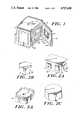
- FIG. 1is a perspective view of a high-density package in accordance with the present invention
- FIGS. 2A, 2B, and 2Care illustrative of body shapes having substantially rectangular, hexagonal, and octagonal cross-sections respectively;
- FIGS. 3A, 3B, 3C, and 3Dillustrate input-output connection techniques for use with the present invention
- FIG. 4is an exploded perspective view of a package in accordance with the present invention.
- FIG. 5is a greatly enlarged perspective view illustrating contact site formation at points where conductive paths terminate in faces of the body
- FIG. 6illustrates a body in accordance with the present invention which is adapted to receive leadless chip carriers
- FIG. 7is illustrative of a body in accordance with the present invention which is adapted to receive leaded chip carriers on respective faces of the body;
- FIG. 8Ais a perspective view of a high-density package in accordance with the present invention in which selected ones of the body faces are adapted to receive an integrated circuit die;
- FIG. 8Bshows selected ones of the layers of FIG. 8A
- FIG. 9illustrates a side elevation view of a package in accordance with the present invention adapted to receive integrated circuit dies on all faces and the top and bottom surface of the body;
- FIG. 10is illustrative of a chip carrier in accordance with the present invention having test and/or connection sites on the normally exposed surface thereof;
- FIG. 11is a perspective view illustrating a heat sink mounted to the high-density package in accordance with the present invention.
- the novel package presently disclosedpermits mounting of integrated circuit elements to all faces of the package and permits true three dimensional interconnection within the package.
- Package constructionwill be understood by reference to FIGS. 1-11.
- the packagecomprises a unitary body 10 formed by cofiring and fusing a plurality of ceramic layers 12 together to form a body having a number of planar faces 14. While typically the body 10 is of cubic shape, the body 10 may be of any other solid geometric form having planar faces. Bodies of rectangular, hexagonal and octagonal cross-section are illustrated in FIGS. 2A, 2B and 2C respectively. Each one of the respective faces 14 may receive an integrated circuit device or devices in the form of an integrated circuit die or dies or an integrated circuit disposed within a standard leadless or leaded chip carrier (FIGS. 6 and 7) or a chip carrier in accordance with the present invention. Additionally, the body faces and/or chip carriers in accordance with the present invention may be adapted to receive discrete electrical components such as chip capacitors, chip resistors and/or thick film resistors and capacitors.
- the bodyhas a bottom layer 16 of ceramic material, having a bottom surface 18 which is typically reserved for input-output connections 20.
- Input-output connectionsmay comprise projecting side brazed input-output pins 22 as shown in FIG. 3A, bottom brazed input-output pins 24 as illustrated in FIG. 3B, a pin 26 grid array as shown in FIG. 3C, or a pad 28 grid array as illustrated in FIG. 3D.
- the bodyhas a height 30 determined by the number and thickness of the respective layers 12.
- the layers 12may vary greatly in thickness and are typically of thickness between 0.8 mils and 100 mils.
- Contact sites 32are provided on the faces 14 of the body in locations where conductive paths 34 disposed on the respective layers 12 terminate in the body faces as seen in FIG. 4 and 5.
- a circuit having a predefined electrical interconnection configurationis provided by interconnecting selected ones of the contact sites 32 with other selected contact sites 32 and interconnecting selected contact sites 32 with selected input-output connections 20. Interconnections are accomplished with conductive paths 34 provided on selected ones of the layers 12 and conductive vias 36 for interconnection of paths 34 on different layers 12.
- the conductive paths 34may be formed by silk screening predetermined patterns of conductive material on selected layers prior to lamination.
- the conductive pathstypically have a cross-section, after firing, of 8 mils by 0.6 mils although conductive path dimensions of 2 mils by 0.5 mils to 8 mils by 8 mils may be readily achieved.
- Conductive vias 36may also be employed to provide contact sites (not shown) on the top or bottom surfaces of the body to permit mating of integrated circuit devices on those surfaces or to provide for connection to input-output connections 20 disposed on the bottom surface, such as bottom brazed input-output pins, a pin grid or a pad grid. Moreover, if the body is fabricated with layers vertically oriented, contact sites on selected body faces are formed by vias 36 and contact sites on the top and bottom surfaces and other selected faces are provided at the locations where conductive paths terminate on the body faces.
- contact sites 38are provided on respective faces 40 of the body 42 to mate with corresponding contacts of leadless chip carriers 44.
- the body 46may be appropriately sized to accomodate one or more leadless chip carriers as shown on respective faces 50 and 52 of the body 46.
- contact sites 54are provided at selected locations on respective faces 56 of the body 58 to mate with corresponding leads 60 of leaded chip carriers 62.
- the bodymay be of size to accomodate one or more leaded chip carriers 62 on each face 56 of the body 58. Additionally, contact sites on selected faces may be oriented to accommodate integrated circuit packages having a pin grid or pad grid array.
- Conductive paths 34are disposed on the layers 12 such that ones of the paths 34 terminate in predetermined lateral positions in the faces 14 thereby determining the lateral position of contact sites 32.
- the height of each contact site 32 on each of the layers 12 with respect to the bottom surface 18is determined by preselection of the thickness of each of the respective layers 12 of the body 10. As previously indicated the contact sites correspond to points where conductive paths terminate in the body faces and are therefore typically of cross-section of 8 mils by 0.6 mils.
- Contact sites 32 corresponding to locations of conductive paths 34 terminationmay be provided with an increased contact area at the body face in a number of ways.
- Layers 12may include channels along intended locations of selected conductive paths 34 or may include recesses at locations of intended contact sites thereby enlarging the area of contact site 32 cross-sections at points of termination of the channels or recesses at the body face 14.
- Respective faces 14may also be silk screened with conductive material to provide enlarged contact areas for respective contact sites 32.
- a ceramic thick film insulatormay be silk screened over respective cube faces 14 so as to provide wells corresponding to intended contact site locations.
- the facesmay then be silk screened in a second operation to fill respective wells with conductive material to form respective contact sites 32.
- a ceramic thick film conductive materialmay alternatively be applied in a post firing operation to locate contact sites with extreme accuracy.
- one or more integrated circuit diesare mounted directly to a face 64 of the body 66.
- a lid 68 of cross-section substantially equivalent to the face 64is provided to encase integrated circuit die 70 between the lid 68 and the respective face 64 of the body 66.
- a seal ring 72is provided on the periphery of each face 64 in accordance with any well-known metallization technique, and the face seal ring 72 mates with a corresponding lid seal ring 74 to hermetically seal the die 70 between the lid 68 and the face 64 upon mating of the lid 68 to the face 64.
- the diemay be mounted on the face 64 of the body 66 and the lid 68 may be provided with a cavity 76 to accomodate the die 70.
- a die receiving cavity 78 or cavitiesmay be provided in respective faces 64 of the body by appropriately notching selected layers 80 of the body as illustrated in FIG. 8B.
- Connection sites 82are disposed on the body face 64 or alternatively as shown in FIGS. 8A and 8B within a notched section 84 of the body face 64.
- Contact sites of the die 70are electrically connected to ones of the connection sites 82 by wire bonding or any other suitable interconnection technique.
- Selected conductive paths 34terminate in areas of connection sites 82 to provide electrical interconnection to the respective connection sites 82.
- the lid 68may be fabricated of a cofired multilayer ceramic material, metal or other suitable material and is secured to the respective body face 64 after wire bonding or connecting by techniques known in the art, respective contact sites of the die 70 to appropriate connection sites 82.
- Test points 86may be provided by including conductive vias in the lid 68 in positions to mate with contact sites 86 disposed on the faces 64 of the body 66. Contact sites 86 are connected with respective connection sites 82 by conductive paths 34 disposed on and conductive vias 36 extending through selected layers 12 of the body 66.
- test points 88 providing electrical access to die 70 contact sites on both the carrier 90 and the face 64may be provided by employing a carrier 90 of the type shown in FIG. 9, of cross-section smaller than the respective face 64. Conductive vias in the carrier 90 terminating in test points 88 mate with an underlying first set of contact sites which are electrically interconnected to a second set of contact sites 92. The second set of contact sites 92 are peripheral to the carrier 90 after mating of respective carriers 90 with the body faces 64 and are therefore accessible for probing.
- integrated circuit die 94are secured within a cavity 96 of a chip carrier 98 fabricated of a plurality of ceramic layers laminated together to form the carrier 98.
- Carrier connection sites 100are disposed within the carrier 98 cavity 96 peripheral to the integrated circuit die 94 permitting wire bonding of die contact sites to respective carrier connection sites 100.
- Carrier contact sites 102are connected to respective carrier connection sites 100 by conductive paths and conductive vias disposed on and extending through respective layers of the carrier 98.
- Carrier contact sites 102are disposed on the face confronting surface of the carrier 98 and are oriented to mate with corresponding face 14 contact sites 32.
- Test point accessis provided by conductive vias extending through layers of the carrier 98.
- the viaselectrically connect to and/or from the carrier 98 contact sites 102.
- the carrier contact sites 102provide test points which are beneficial for testing both before assembly of the carrier 98 to the face 14 and after final assembly of the carrier 98 and body 10.
- a carrier 104may be of smaller cross-section than the face 14 (FIG. 1) to which it is mated.
- One or more integrated circuit diesmay be disposed within a given carrier, the size of the carrier and body being adjusted as desired for a specific circuit application.
- a metallized seal ring 106(FIG. 1) is typically disposed around the periphery of a die receiving carrier 98 to mate with a corresponding metallized seal ring 108 on the body face 14 thereby achieving hermetic encapsulation of integrated circuit die or dies between the carrier 98 and body face 14.
- a seal ring 110may be disposed interior to carrier 104 contact sites 106 permitting visual inspection of mating carrier and face contact sites after assembly of the carrier 104 to the respective face 14.
- Contact sites 106may be raised to facilitate inspection of the sites and solder flux cleaning after mating of the carrier 104 to the respective body face 14.
- any of the above-described embodimentsmay be provided with a bore 112 (FIG. 1) extending from the top surface of the body partially through to the bottom surface or entirely through the body 10.
- the bore 112may be metallized and sized to receive a heat sink 114 to faciitate heat dissipation from the element as shown in FIG. 11.
- the elementmay be fluid cooled by passage of fluid through the bore 112 providing further improvement of heat dissipation characteristics.
- a bodyformed in accordance with the above disclosure may be adapted to receive, memory, microcomputer, gate array, buffer, peripheral or other integrated circuit devices on the respective faces of the body.
- a carrier 104 of multilayer ceramic material of the type shown in FIG. 10is adapted to receive four 256 kilobit memory elements. Respective die contact sites of the four memory element dies are wire bonded to carrier connection sites provided peripheral to each respective memory element die and the die we electronically tested on the carrier 104. The connection sites are electrically connected to carrier contact sites peripherally disposed with respect to the carrier connection sites. Contact sites are disposed on respective planar faces of a multilayer ceramic unitary body to mate with corresponding carrier contact sites. Contact sites on respective faces are electrically interconnected in accordance with the present disclosure and selectively interconnected with input-output connections projecting from the bottom surface of the body.
- One carriercontaining four 256 Kilobit memory elements is electrically and hermetically mated to each of four faces of a substantially cubic body to form a four megabit memory element.
- a metallized bore extending through the bodyis provided with a heat sink to facilitate heat dissipation and improved operational reliability of the four megabit memory element.
- a thermally conductive elastomermay be employed to facilitate heat conduction from the body to the heat sink.
- the heat sinkmay be in thermal conducting relation with selected die carriers.
- chip capacitorsmay be mounted to selected faces of the body or alternatively, to contact sites within or on the carriers 104 specifically provided and oriented to receive the chip capacitors.
Landscapes
- Physics & Mathematics (AREA)
- Condensed Matter Physics & Semiconductors (AREA)
- General Physics & Mathematics (AREA)
- Engineering & Computer Science (AREA)
- Computer Hardware Design (AREA)
- Microelectronics & Electronic Packaging (AREA)
- Power Engineering (AREA)
- Production Of Multi-Layered Print Wiring Board (AREA)
- Lead Frames For Integrated Circuits (AREA)
Abstract
Description
Claims (30)
Priority Applications (2)
| Application Number | Priority Date | Filing Date | Title |
|---|---|---|---|
| US06/555,032US4727410A (en) | 1983-11-23 | 1983-11-23 | High density integrated circuit package |
| JP59247873AJPS60233842A (en) | 1983-11-23 | 1984-11-22 | High density integrated circuit package |
Applications Claiming Priority (1)
| Application Number | Priority Date | Filing Date | Title |
|---|---|---|---|
| US06/555,032US4727410A (en) | 1983-11-23 | 1983-11-23 | High density integrated circuit package |
Publications (1)
| Publication Number | Publication Date |
|---|---|
| US4727410Atrue US4727410A (en) | 1988-02-23 |
Family
ID=24215701
Family Applications (1)
| Application Number | Title | Priority Date | Filing Date |
|---|---|---|---|
| US06/555,032Expired - LifetimeUS4727410A (en) | 1983-11-23 | 1983-11-23 | High density integrated circuit package |
Country Status (2)
| Country | Link |
|---|---|
| US (1) | US4727410A (en) |
| JP (1) | JPS60233842A (en) |
Cited By (81)
| Publication number | Priority date | Publication date | Assignee | Title |
|---|---|---|---|---|
| US4814857A (en)* | 1987-02-25 | 1989-03-21 | International Business Machines Corporation | Circuit module with separate signal and power connectors |
| WO1989005066A1 (en)* | 1987-11-16 | 1989-06-01 | Motorola, Inc. | Moldable/foldable radio housing |
| US4868712A (en)* | 1987-02-04 | 1989-09-19 | Woodman John K | Three dimensional integrated circuit package |
| US4983533A (en)* | 1987-10-28 | 1991-01-08 | Irvine Sensors Corporation | High-density electronic modules - process and product |
| US5016138A (en)* | 1987-10-27 | 1991-05-14 | Woodman John K | Three dimensional integrated circuit package |
| US5031027A (en)* | 1990-07-13 | 1991-07-09 | Motorola, Inc. | Shielded electrical circuit |
| US5068715A (en)* | 1990-06-29 | 1991-11-26 | Digital Equipment Corporation | High-power, high-performance integrated circuit chip package |
| US5146782A (en)* | 1987-11-13 | 1992-09-15 | Rasmussen Torben B | Flowmeter |
| US5170245A (en)* | 1988-06-15 | 1992-12-08 | International Business Machines Corp. | Semiconductor device having metallic interconnects formed by grit blasting |
| US5291062A (en)* | 1993-03-01 | 1994-03-01 | Motorola, Inc. | Area array semiconductor device having a lid with functional contacts |
| USD345963S (en) | 1991-10-30 | 1994-04-12 | Sanyo Electric Co., Ltd. | Hybrid integrated circuit |
| US5309318A (en)* | 1992-04-21 | 1994-05-03 | International Business Machines Corporation | Thermally enhanced semiconductor chip package |
| EP0429759B1 (en)* | 1989-11-22 | 1994-10-26 | International Business Machines Corporation | Three dimensional microelectronic packaging |
| US5374196A (en)* | 1992-10-07 | 1994-12-20 | Fujitsu Limited | High-density/long-via laminated connector |
| US5396032A (en)* | 1993-05-04 | 1995-03-07 | Alcatel Network Systems, Inc. | Method and apparatus for providing electrical access to devices in a multi-chip module |
| US5412247A (en)* | 1989-07-28 | 1995-05-02 | The Charles Stark Draper Laboratory, Inc. | Protection and packaging system for semiconductor devices |
| US5426566A (en)* | 1991-09-30 | 1995-06-20 | International Business Machines Corporation | Multichip integrated circuit packages and systems |
| US5426563A (en)* | 1992-08-05 | 1995-06-20 | Fujitsu Limited | Three-dimensional multichip module |
| US5502667A (en)* | 1993-09-13 | 1996-03-26 | International Business Machines Corporation | Integrated multichip memory module structure |
| US5512710A (en)* | 1992-08-21 | 1996-04-30 | Cts Corporation | Multilayer package with second layer via test connections |
| US5561622A (en)* | 1993-09-13 | 1996-10-01 | International Business Machines Corporation | Integrated memory cube structure |
| US5561593A (en)* | 1994-01-27 | 1996-10-01 | Vicon Enterprises, Inc. | Z-interface-board |
| US5568361A (en)* | 1992-03-17 | 1996-10-22 | Massachusetts Institute Of Technology | Three-dimensional electronic circuit of interconnected modules |
| US5648684A (en)* | 1995-07-26 | 1997-07-15 | International Business Machines Corporation | Endcap chip with conductive, monolithic L-connect for multichip stack |
| US5691885A (en)* | 1992-03-17 | 1997-11-25 | Massachusetts Institute Of Technology | Three-dimensional interconnect having modules with vertical top and bottom connectors |
| US5703747A (en)* | 1995-02-22 | 1997-12-30 | Voldman; Steven Howard | Multichip semiconductor structures with interchip electrostatic discharge protection, and fabrication methods therefore |
| US5731945A (en)* | 1995-02-22 | 1998-03-24 | International Business Machines Corporation | Multichip semiconductor structures with consolidated circuitry and programmable ESD protection for input/output nodes |
| US5781413A (en)* | 1996-09-30 | 1998-07-14 | International Business Machines Corporation | Method and apparatus for directing the input/output connection of integrated circuit chip cube configurations |
| US5815374A (en)* | 1996-09-30 | 1998-09-29 | International Business Machines Corporation | Method and apparatus for redirecting certain input/output connections of integrated circuit chip configurations |
| US5854534A (en)* | 1992-08-05 | 1998-12-29 | Fujitsu Limited | Controlled impedence interposer substrate |
| US5952611A (en)* | 1997-12-19 | 1999-09-14 | Texas Instruments Incorporated | Flexible pin location integrated circuit package |
| US5956233A (en)* | 1997-12-19 | 1999-09-21 | Texas Instruments Incorporated | High density single inline memory module |
| US5998860A (en)* | 1997-12-19 | 1999-12-07 | Texas Instruments Incorporated | Double sided single inline memory module |
| US6049129A (en)* | 1997-12-19 | 2000-04-11 | Texas Instruments Incorporated | Chip size integrated circuit package |
| US6084306A (en)* | 1998-05-29 | 2000-07-04 | Texas Instruments Incorporated | Bridging method of interconnects for integrated circuit packages |
| US6087203A (en)* | 1997-12-19 | 2000-07-11 | Texas Instruments Incorporated | Method for adhering and sealing a silicon chip in an integrated circuit package |
| US6089095A (en)* | 1997-12-19 | 2000-07-18 | Texas Instruments Incorporated | Method and apparatus for nondestructive inspection and defect detection in packaged integrated circuits |
| US6137691A (en)* | 1997-10-10 | 2000-10-24 | Samsung Electronics Co., Ltd. | Three dimensional composite circuit board |
| US6177723B1 (en) | 1997-04-10 | 2001-01-23 | Texas Instruments Incorporated | Integrated circuit package and flat plate molding process for integrated circuit package |
| US6274929B1 (en) | 1998-09-01 | 2001-08-14 | Texas Instruments Incorporated | Stacked double sided integrated circuit package |
| US6320126B1 (en)* | 1998-07-14 | 2001-11-20 | Texas Instruments Incorporated | Vertical ball grid array integrated circuit package |
| US6392293B2 (en) | 1998-06-04 | 2002-05-21 | Kabushiki Kaisha Toshiba | Semiconductor package with sloped outer leads |
| US20020155728A1 (en)* | 1990-09-24 | 2002-10-24 | Tessera, Inc. | Semiconductor chip assemblies, methods of making same and components for same |
| USD471515S1 (en) | 2001-07-27 | 2003-03-11 | Matsushita Electric Industrial Co., Ltd. | Battery |
| US6549420B2 (en)* | 1996-10-31 | 2003-04-15 | Hewlett-Packard Development Company, L.P. | Method and apparatus for increasing memory capacity |
| US6555399B1 (en)* | 1991-03-26 | 2003-04-29 | Micron Technology, Inc. | Double-packaged multichip semiconductor module |
| US6624506B2 (en) | 2000-04-20 | 2003-09-23 | Kabushiki Kaisha Toshiba | Multichip semiconductor device and memory card |
| US6667560B2 (en) | 1996-05-29 | 2003-12-23 | Texas Instruments Incorporated | Board on chip ball grid array |
| US6768646B1 (en) | 1998-01-23 | 2004-07-27 | Texas Instruments Incorporated | High density internal ball grid array integrated circuit package |
| USD498698S1 (en) | 2003-06-19 | 2004-11-23 | Ofer Davidi | Irregular octagonal diamond cut |
| USD506670S1 (en)* | 2003-11-11 | 2005-06-28 | Moab Brewers, Llc | Beverage container package |
| US20050218495A1 (en)* | 1990-09-24 | 2005-10-06 | Tessera, Inc. | Microelectronic assembly having encapsulated wire bonding leads |
| USD512635S1 (en)* | 2004-06-23 | 2005-12-13 | Crown Packaging Technology, Inc. | Closure |
| USD542331S1 (en)* | 2004-09-10 | 2007-05-08 | Casio Keisanki Kabushiki Kaisha | Cash register |
| US20100008034A1 (en)* | 2008-07-14 | 2010-01-14 | International Business Machines Corporation | Tubular memory module |
| USD649987S1 (en)* | 2010-02-04 | 2011-12-06 | Dunnahoe Duane C | Carbide chip |
| US20140334120A1 (en)* | 2012-05-17 | 2014-11-13 | Eagantu Ltd. | Electronic module allowing fine tuning after assembly |
| USD771788S1 (en)* | 2014-01-20 | 2016-11-15 | Turbotec Products, Inc. | Insulated housing for coiled heat exchanger tube |
| USD816615S1 (en)* | 2015-07-20 | 2018-05-01 | Shenzhen Royole Technologies Co., Ltd. | Power adapter |
| USD854636S1 (en)* | 2016-07-13 | 2019-07-23 | The Prophet Corporation | Exercise tire |
| USD857156S1 (en)* | 2016-11-02 | 2019-08-20 | Innovative Water Care, Llc | Chemical tablet for aquatic systems |
| US10916524B2 (en)* | 2016-12-29 | 2021-02-09 | Intel Corporation | Stacked dice systems |
| US11351094B2 (en) | 2017-05-16 | 2022-06-07 | The Procter And Gamble Company | Conditioning hair care compositions in the form of dissolvable solid structures |
| US11352474B2 (en) | 2014-04-22 | 2022-06-07 | The Procter And Gamble Company | Compositions in the form of dissolvable solid structures |
| US11395789B2 (en) | 2017-01-27 | 2022-07-26 | The Procter & Gamble Company | Compositions in the form of dissolvable solid structures |
| US11419808B2 (en) | 2019-07-03 | 2022-08-23 | The Procter & Gamble Company | Fibrous structures containing cationic surfactants and soluble acids |
| USD962050S1 (en) | 2020-03-20 | 2022-08-30 | The Procter And Gamble Company | Primary package for a solid, single dose beauty care composition |
| US11525104B2 (en) | 2019-11-20 | 2022-12-13 | The Procter & Gamble Company | Porous dissolvable solid structure |
| USD980060S1 (en) | 2018-07-16 | 2023-03-07 | The Procter & Gamble Company | Container |
| US11597191B2 (en) | 2019-10-14 | 2023-03-07 | The Procter & Gamble Company | Biodegradable and/or home compostable sachet containing a solid article |
| US11666514B2 (en) | 2018-09-21 | 2023-06-06 | The Procter & Gamble Company | Fibrous structures containing polymer matrix particles with perfume ingredients |
| US11679066B2 (en) | 2019-06-28 | 2023-06-20 | The Procter & Gamble Company | Dissolvable solid fibrous articles containing anionic surfactants |
| USD1007328S1 (en) | 2019-10-01 | 2023-12-12 | The Procter & Gamble Company | Packaging for a single dose personal care product |
| US11925698B2 (en) | 2020-07-31 | 2024-03-12 | The Procter & Gamble Company | Water-soluble fibrous pouch containing prills for hair care |
| US11944696B2 (en) | 2010-07-02 | 2024-04-02 | The Procter & Gamble Company | Detergent product and method for making same |
| US11944693B2 (en) | 2010-07-02 | 2024-04-02 | The Procter & Gamble Company | Method for delivering an active agent |
| US11951194B2 (en) | 2017-01-27 | 2024-04-09 | The Procter & Gamble Company | Compositions in the form of dissolvable solid structures comprising effervescent agglomerated particles |
| US11970789B2 (en) | 2010-07-02 | 2024-04-30 | The Procter & Gamble Company | Filaments comprising an active agent nonwoven webs and methods for making same |
| USD1045064S1 (en) | 2020-12-17 | 2024-10-01 | The Procter & Gamble Company | Single-dose dissolvable personal care unit |
| US12403083B2 (en) | 2021-08-30 | 2025-09-02 | The Procter & Gamble Company | Dissolvable solid structure comprising first and second polymeric structurants |
| US12416103B2 (en) | 2010-07-02 | 2025-09-16 | The Procter & Gamble Company | Dissolvable fibrous web structure article comprising active agents |
Citations (12)
| Publication number | Priority date | Publication date | Assignee | Title |
|---|---|---|---|---|
| US3346773A (en)* | 1967-10-10 | Multilayer conductor board assembly | ||
| US3545079A (en)* | 1968-05-02 | 1970-12-08 | Vitramon Inc | Method of making multilayer circuit system |
| US3546776A (en)* | 1962-09-06 | 1970-12-15 | Aerovox Corp | Process for manufacturing a ceramic multilayer circuit module |
| US3968193A (en)* | 1971-08-27 | 1976-07-06 | International Business Machines Corporation | Firing process for forming a multilayer glass-metal module |
| US4245273A (en)* | 1979-06-29 | 1981-01-13 | International Business Machines Corporation | Package for mounting and interconnecting a plurality of large scale integrated semiconductor devices |
| WO1981002367A1 (en)* | 1980-02-12 | 1981-08-20 | Mostek Corp | Over/under dual in-line chip package |
| US4322778A (en)* | 1980-01-25 | 1982-03-30 | International Business Machines Corp. | High performance semiconductor package assembly |
| US4328530A (en)* | 1980-06-30 | 1982-05-04 | International Business Machines Corporation | Multiple layer, ceramic carrier for high switching speed VLSI chips |
| US4345955A (en)* | 1980-10-28 | 1982-08-24 | E. I. Du Pont De Nemours And Company | Process for manufacturing multilayer ceramic chip carrier modules |
| US4349862A (en)* | 1980-08-11 | 1982-09-14 | International Business Machines Corporation | Capacitive chip carrier and multilayer ceramic capacitors |
| US4549200A (en)* | 1982-07-08 | 1985-10-22 | International Business Machines Corporation | Repairable multi-level overlay system for semiconductor device |
| US4608592A (en)* | 1982-07-09 | 1986-08-26 | Nec Corporation | Semiconductor device provided with a package for a semiconductor element having a plurality of electrodes to be applied with substantially same voltage |
- 1983
- 1983-11-23USUS06/555,032patent/US4727410A/ennot_activeExpired - Lifetime
- 1984
- 1984-11-22JPJP59247873Apatent/JPS60233842A/enactivePending
Patent Citations (12)
| Publication number | Priority date | Publication date | Assignee | Title |
|---|---|---|---|---|
| US3346773A (en)* | 1967-10-10 | Multilayer conductor board assembly | ||
| US3546776A (en)* | 1962-09-06 | 1970-12-15 | Aerovox Corp | Process for manufacturing a ceramic multilayer circuit module |
| US3545079A (en)* | 1968-05-02 | 1970-12-08 | Vitramon Inc | Method of making multilayer circuit system |
| US3968193A (en)* | 1971-08-27 | 1976-07-06 | International Business Machines Corporation | Firing process for forming a multilayer glass-metal module |
| US4245273A (en)* | 1979-06-29 | 1981-01-13 | International Business Machines Corporation | Package for mounting and interconnecting a plurality of large scale integrated semiconductor devices |
| US4322778A (en)* | 1980-01-25 | 1982-03-30 | International Business Machines Corp. | High performance semiconductor package assembly |
| WO1981002367A1 (en)* | 1980-02-12 | 1981-08-20 | Mostek Corp | Over/under dual in-line chip package |
| US4328530A (en)* | 1980-06-30 | 1982-05-04 | International Business Machines Corporation | Multiple layer, ceramic carrier for high switching speed VLSI chips |
| US4349862A (en)* | 1980-08-11 | 1982-09-14 | International Business Machines Corporation | Capacitive chip carrier and multilayer ceramic capacitors |
| US4345955A (en)* | 1980-10-28 | 1982-08-24 | E. I. Du Pont De Nemours And Company | Process for manufacturing multilayer ceramic chip carrier modules |
| US4549200A (en)* | 1982-07-08 | 1985-10-22 | International Business Machines Corporation | Repairable multi-level overlay system for semiconductor device |
| US4608592A (en)* | 1982-07-09 | 1986-08-26 | Nec Corporation | Semiconductor device provided with a package for a semiconductor element having a plurality of electrodes to be applied with substantially same voltage |
Non-Patent Citations (4)
| Title |
|---|
| Arnold et al., IBM Tech. Disc. Bull., 9(6), Nov. 1966, "Fabrication of Multilayer Ceramic Structure . . .", pp. 565-566. |
| Arnold et al., IBM Tech. Disc. Bull., 9(6), Nov. 1966, Fabrication of Multilayer Ceramic Structure . . . , pp. 565 566.* |
| Benenati et al., IBM Tech. Disc. Bull., 10(12), May 1968, "Circuit Package", pp. 1977-1978. |
| Benenati et al., IBM Tech. Disc. Bull., 10(12), May 1968, Circuit Package , pp. 1977 1978.* |
Cited By (101)
| Publication number | Priority date | Publication date | Assignee | Title |
|---|---|---|---|---|
| US4868712A (en)* | 1987-02-04 | 1989-09-19 | Woodman John K | Three dimensional integrated circuit package |
| US4814857A (en)* | 1987-02-25 | 1989-03-21 | International Business Machines Corporation | Circuit module with separate signal and power connectors |
| US5016138A (en)* | 1987-10-27 | 1991-05-14 | Woodman John K | Three dimensional integrated circuit package |
| US4983533A (en)* | 1987-10-28 | 1991-01-08 | Irvine Sensors Corporation | High-density electronic modules - process and product |
| US5146782A (en)* | 1987-11-13 | 1992-09-15 | Rasmussen Torben B | Flowmeter |
| WO1989005066A1 (en)* | 1987-11-16 | 1989-06-01 | Motorola, Inc. | Moldable/foldable radio housing |
| US4939792A (en)* | 1987-11-16 | 1990-07-03 | Motorola, Inc. | Moldable/foldable radio housing |
| US5170245A (en)* | 1988-06-15 | 1992-12-08 | International Business Machines Corp. | Semiconductor device having metallic interconnects formed by grit blasting |
| US5412247A (en)* | 1989-07-28 | 1995-05-02 | The Charles Stark Draper Laboratory, Inc. | Protection and packaging system for semiconductor devices |
| EP0429759B1 (en)* | 1989-11-22 | 1994-10-26 | International Business Machines Corporation | Three dimensional microelectronic packaging |
| US5068715A (en)* | 1990-06-29 | 1991-11-26 | Digital Equipment Corporation | High-power, high-performance integrated circuit chip package |
| US5031027A (en)* | 1990-07-13 | 1991-07-09 | Motorola, Inc. | Shielded electrical circuit |
| US20020155728A1 (en)* | 1990-09-24 | 2002-10-24 | Tessera, Inc. | Semiconductor chip assemblies, methods of making same and components for same |
| US20050218495A1 (en)* | 1990-09-24 | 2005-10-06 | Tessera, Inc. | Microelectronic assembly having encapsulated wire bonding leads |
| US7291910B2 (en) | 1990-09-24 | 2007-11-06 | Tessera, Inc. | Semiconductor chip assemblies, methods of making same and components for same |
| US20030155649A1 (en)* | 1991-03-26 | 2003-08-21 | Wood Alan G. | Double-packaged multi-chip semiconductor module |
| US6555399B1 (en)* | 1991-03-26 | 2003-04-29 | Micron Technology, Inc. | Double-packaged multichip semiconductor module |
| US7259450B2 (en) | 1991-03-26 | 2007-08-21 | Micron Technology, Inc. | Double-packaged multi-chip semiconductor module |
| US5426566A (en)* | 1991-09-30 | 1995-06-20 | International Business Machines Corporation | Multichip integrated circuit packages and systems |
| USD345963S (en) | 1991-10-30 | 1994-04-12 | Sanyo Electric Co., Ltd. | Hybrid integrated circuit |
| US5568361A (en)* | 1992-03-17 | 1996-10-22 | Massachusetts Institute Of Technology | Three-dimensional electronic circuit of interconnected modules |
| US5691885A (en)* | 1992-03-17 | 1997-11-25 | Massachusetts Institute Of Technology | Three-dimensional interconnect having modules with vertical top and bottom connectors |
| US5309318A (en)* | 1992-04-21 | 1994-05-03 | International Business Machines Corporation | Thermally enhanced semiconductor chip package |
| US5655290A (en)* | 1992-08-05 | 1997-08-12 | Fujitsu Limited | Method for making a three-dimensional multichip module |
| US5854534A (en)* | 1992-08-05 | 1998-12-29 | Fujitsu Limited | Controlled impedence interposer substrate |
| US6102710A (en)* | 1992-08-05 | 2000-08-15 | Fujitsu Limited | Controlled impedance interposer substrate and method of making |
| US5426563A (en)* | 1992-08-05 | 1995-06-20 | Fujitsu Limited | Three-dimensional multichip module |
| US5512710A (en)* | 1992-08-21 | 1996-04-30 | Cts Corporation | Multilayer package with second layer via test connections |
| US5374196A (en)* | 1992-10-07 | 1994-12-20 | Fujitsu Limited | High-density/long-via laminated connector |
| US5291062A (en)* | 1993-03-01 | 1994-03-01 | Motorola, Inc. | Area array semiconductor device having a lid with functional contacts |
| US5396032A (en)* | 1993-05-04 | 1995-03-07 | Alcatel Network Systems, Inc. | Method and apparatus for providing electrical access to devices in a multi-chip module |
| US5561622A (en)* | 1993-09-13 | 1996-10-01 | International Business Machines Corporation | Integrated memory cube structure |
| US5502667A (en)* | 1993-09-13 | 1996-03-26 | International Business Machines Corporation | Integrated multichip memory module structure |
| US5561593A (en)* | 1994-01-27 | 1996-10-01 | Vicon Enterprises, Inc. | Z-interface-board |
| US5731945A (en)* | 1995-02-22 | 1998-03-24 | International Business Machines Corporation | Multichip semiconductor structures with consolidated circuitry and programmable ESD protection for input/output nodes |
| US5943254A (en)* | 1995-02-22 | 1999-08-24 | International Business Machines Corporation | Multichip semiconductor structures with consolidated circuitry and programmable ESD protection for input/output nodes |
| US5703747A (en)* | 1995-02-22 | 1997-12-30 | Voldman; Steven Howard | Multichip semiconductor structures with interchip electrostatic discharge protection, and fabrication methods therefore |
| US5807791A (en)* | 1995-02-22 | 1998-09-15 | International Business Machines Corporation | Methods for fabricating multichip semiconductor structures with consolidated circuitry and programmable ESD protection for input/output nodes |
| US5930098A (en)* | 1995-02-22 | 1999-07-27 | International Business Machines Corporation | Multichip semiconductor structures with interchip electrostatic discharge protection, and fabrication methods therefore |
| US5648684A (en)* | 1995-07-26 | 1997-07-15 | International Business Machines Corporation | Endcap chip with conductive, monolithic L-connect for multichip stack |
| US6667560B2 (en) | 1996-05-29 | 2003-12-23 | Texas Instruments Incorporated | Board on chip ball grid array |
| US5781413A (en)* | 1996-09-30 | 1998-07-14 | International Business Machines Corporation | Method and apparatus for directing the input/output connection of integrated circuit chip cube configurations |
| US5815374A (en)* | 1996-09-30 | 1998-09-29 | International Business Machines Corporation | Method and apparatus for redirecting certain input/output connections of integrated circuit chip configurations |
| US6549420B2 (en)* | 1996-10-31 | 2003-04-15 | Hewlett-Packard Development Company, L.P. | Method and apparatus for increasing memory capacity |
| US6177723B1 (en) | 1997-04-10 | 2001-01-23 | Texas Instruments Incorporated | Integrated circuit package and flat plate molding process for integrated circuit package |
| US6137691A (en)* | 1997-10-10 | 2000-10-24 | Samsung Electronics Co., Ltd. | Three dimensional composite circuit board |
| US6049129A (en)* | 1997-12-19 | 2000-04-11 | Texas Instruments Incorporated | Chip size integrated circuit package |
| US6387729B2 (en) | 1997-12-19 | 2002-05-14 | Texas Instruments Incorporated | Method for adhering and sealing a silicon chip in an integrated circuit package |
| US5952611A (en)* | 1997-12-19 | 1999-09-14 | Texas Instruments Incorporated | Flexible pin location integrated circuit package |
| US6089095A (en)* | 1997-12-19 | 2000-07-18 | Texas Instruments Incorporated | Method and apparatus for nondestructive inspection and defect detection in packaged integrated circuits |
| US6087203A (en)* | 1997-12-19 | 2000-07-11 | Texas Instruments Incorporated | Method for adhering and sealing a silicon chip in an integrated circuit package |
| US5998860A (en)* | 1997-12-19 | 1999-12-07 | Texas Instruments Incorporated | Double sided single inline memory module |
| US5956233A (en)* | 1997-12-19 | 1999-09-21 | Texas Instruments Incorporated | High density single inline memory module |
| US6768646B1 (en) | 1998-01-23 | 2004-07-27 | Texas Instruments Incorporated | High density internal ball grid array integrated circuit package |
| US6084306A (en)* | 1998-05-29 | 2000-07-04 | Texas Instruments Incorporated | Bridging method of interconnects for integrated circuit packages |
| US6392293B2 (en) | 1998-06-04 | 2002-05-21 | Kabushiki Kaisha Toshiba | Semiconductor package with sloped outer leads |
| US6420782B1 (en) | 1998-07-14 | 2002-07-16 | Texas Instruments Incorporated | Vertical ball grid array integrated circuit package |
| US6320126B1 (en)* | 1998-07-14 | 2001-11-20 | Texas Instruments Incorporated | Vertical ball grid array integrated circuit package |
| US6274929B1 (en) | 1998-09-01 | 2001-08-14 | Texas Instruments Incorporated | Stacked double sided integrated circuit package |
| US6624506B2 (en) | 2000-04-20 | 2003-09-23 | Kabushiki Kaisha Toshiba | Multichip semiconductor device and memory card |
| USD471515S1 (en) | 2001-07-27 | 2003-03-11 | Matsushita Electric Industrial Co., Ltd. | Battery |
| USD498698S1 (en) | 2003-06-19 | 2004-11-23 | Ofer Davidi | Irregular octagonal diamond cut |
| USD506670S1 (en)* | 2003-11-11 | 2005-06-28 | Moab Brewers, Llc | Beverage container package |
| USD512635S1 (en)* | 2004-06-23 | 2005-12-13 | Crown Packaging Technology, Inc. | Closure |
| USD542331S1 (en)* | 2004-09-10 | 2007-05-08 | Casio Keisanki Kabushiki Kaisha | Cash register |
| US20100008034A1 (en)* | 2008-07-14 | 2010-01-14 | International Business Machines Corporation | Tubular memory module |
| US8000105B2 (en) | 2008-07-14 | 2011-08-16 | International Business Machines Corporation | Tubular memory module |
| USD649987S1 (en)* | 2010-02-04 | 2011-12-06 | Dunnahoe Duane C | Carbide chip |
| US11944696B2 (en) | 2010-07-02 | 2024-04-02 | The Procter & Gamble Company | Detergent product and method for making same |
| US12416103B2 (en) | 2010-07-02 | 2025-09-16 | The Procter & Gamble Company | Dissolvable fibrous web structure article comprising active agents |
| US12194118B2 (en) | 2010-07-02 | 2025-01-14 | The Procter & Gamble Company | Detergent product and method for making same |
| US11970789B2 (en) | 2010-07-02 | 2024-04-30 | The Procter & Gamble Company | Filaments comprising an active agent nonwoven webs and methods for making same |
| US11944693B2 (en) | 2010-07-02 | 2024-04-02 | The Procter & Gamble Company | Method for delivering an active agent |
| US20140334120A1 (en)* | 2012-05-17 | 2014-11-13 | Eagantu Ltd. | Electronic module allowing fine tuning after assembly |
| US9155198B2 (en)* | 2012-05-17 | 2015-10-06 | Eagantu Ltd. | Electronic module allowing fine tuning after assembly |
| USD771788S1 (en)* | 2014-01-20 | 2016-11-15 | Turbotec Products, Inc. | Insulated housing for coiled heat exchanger tube |
| US11352474B2 (en) | 2014-04-22 | 2022-06-07 | The Procter And Gamble Company | Compositions in the form of dissolvable solid structures |
| USD816615S1 (en)* | 2015-07-20 | 2018-05-01 | Shenzhen Royole Technologies Co., Ltd. | Power adapter |
| USD854636S1 (en)* | 2016-07-13 | 2019-07-23 | The Prophet Corporation | Exercise tire |
| USD857156S1 (en)* | 2016-11-02 | 2019-08-20 | Innovative Water Care, Llc | Chemical tablet for aquatic systems |
| US10916524B2 (en)* | 2016-12-29 | 2021-02-09 | Intel Corporation | Stacked dice systems |
| US11529292B2 (en) | 2017-01-27 | 2022-12-20 | The Procter & Gamble Company | Compositions in the form of dissolvable solid structures |
| US11951194B2 (en) | 2017-01-27 | 2024-04-09 | The Procter & Gamble Company | Compositions in the form of dissolvable solid structures comprising effervescent agglomerated particles |
| US11395789B2 (en) | 2017-01-27 | 2022-07-26 | The Procter & Gamble Company | Compositions in the form of dissolvable solid structures |
| US12029799B2 (en) | 2017-05-16 | 2024-07-09 | The Procter & Gamble Company | Conditioning hair care compositions in the form of dissolvable solid structures |
| US11351094B2 (en) | 2017-05-16 | 2022-06-07 | The Procter And Gamble Company | Conditioning hair care compositions in the form of dissolvable solid structures |
| USD980060S1 (en) | 2018-07-16 | 2023-03-07 | The Procter & Gamble Company | Container |
| US11666514B2 (en) | 2018-09-21 | 2023-06-06 | The Procter & Gamble Company | Fibrous structures containing polymer matrix particles with perfume ingredients |
| US11679066B2 (en) | 2019-06-28 | 2023-06-20 | The Procter & Gamble Company | Dissolvable solid fibrous articles containing anionic surfactants |
| US11419808B2 (en) | 2019-07-03 | 2022-08-23 | The Procter & Gamble Company | Fibrous structures containing cationic surfactants and soluble acids |
| USD1062448S1 (en) | 2019-10-01 | 2025-02-18 | The Procter & Gamble Company | Packaging for a single dose personal care product |
| USD1007328S1 (en) | 2019-10-01 | 2023-12-12 | The Procter & Gamble Company | Packaging for a single dose personal care product |
| US11597191B2 (en) | 2019-10-14 | 2023-03-07 | The Procter & Gamble Company | Biodegradable and/or home compostable sachet containing a solid article |
| US12280573B2 (en) | 2019-10-14 | 2025-04-22 | The Procter & Gamble Company | Biodegradable and/or home compostable sachet containing a solid article |
| US11525104B2 (en) | 2019-11-20 | 2022-12-13 | The Procter & Gamble Company | Porous dissolvable solid structure |
| USD966089S1 (en) | 2020-03-20 | 2022-10-11 | The Procter & Gamble Company | Primary package for a solid, single dose beauty care composition |
| USD966088S1 (en) | 2020-03-20 | 2022-10-11 | The Procter & Gamble Company | Primary package for a solid, single dose beauty care composition |
| USD962050S1 (en) | 2020-03-20 | 2022-08-30 | The Procter And Gamble Company | Primary package for a solid, single dose beauty care composition |
| US11925698B2 (en) | 2020-07-31 | 2024-03-12 | The Procter & Gamble Company | Water-soluble fibrous pouch containing prills for hair care |
| USD1045064S1 (en) | 2020-12-17 | 2024-10-01 | The Procter & Gamble Company | Single-dose dissolvable personal care unit |
| US12403083B2 (en) | 2021-08-30 | 2025-09-02 | The Procter & Gamble Company | Dissolvable solid structure comprising first and second polymeric structurants |
Also Published As
| Publication number | Publication date |
|---|---|
| JPS60233842A (en) | 1985-11-20 |
Similar Documents
| Publication | Publication Date | Title |
|---|---|---|
| US4727410A (en) | High density integrated circuit package | |
| US4616406A (en) | Process of making a semiconductor device having parallel leads directly connected perpendicular to integrated circuit layers therein | |
| US5701233A (en) | Stackable modules and multimodular assemblies | |
| US5943213A (en) | Three-dimensional electronic module | |
| US5016138A (en) | Three dimensional integrated circuit package | |
| US7061096B2 (en) | Multi-surface IC packaging structures and methods for their manufacture | |
| US4437141A (en) | High terminal count integrated circuit device package | |
| US5434745A (en) | Stacked silicon die carrier assembly | |
| US3872583A (en) | LSI chip package and method | |
| US6020629A (en) | Stacked semiconductor package and method of fabrication | |
| US6195268B1 (en) | Stacking layers containing enclosed IC chips | |
| KR0135585B1 (en) | Package and semiconductor device for semiconductor devices | |
| JP2703745B2 (en) | Multi die package equipment | |
| US5766975A (en) | Packaged integrated circuit having thermal enhancement and reduced footprint size | |
| JP2547637B2 (en) | Pin grid array package structure | |
| US5751554A (en) | Testable chip carrier | |
| JPS61502294A (en) | High density IC module assembly | |
| JPH0613541A (en) | Three-dimensional multichip semiconductor device which can be laminated and manufacture thereof | |
| JP2002543618A (en) | Stackable flex circuit IC package and method of manufacturing the same | |
| US4920454A (en) | Wafer scale package system and header and method of manufacture thereof | |
| WO2000031797A2 (en) | Device for electronic packaging, pin jig fixture | |
| US4731700A (en) | Semiconductor connection and crossover apparatus | |
| US6495400B1 (en) | Method of forming low profile semiconductor package | |
| JPS6356706B2 (en) | ||
| JPH08250651A (en) | Semiconductor package |
Legal Events
| Date | Code | Title | Description |
|---|---|---|---|
| AS | Assignment | Owner name:AUGAT INCORPORATED, 87 JOHN DIETSCH SQUARE, P.O. Free format text:ASSIGNMENT OF ASSIGNORS INTEREST.;ASSIGNOR:HIGGINS, LEO M. III;REEL/FRAME:004200/0548 Effective date:19831116 Owner name:AUGAT INCORPORATED, MASSACHUSETTS Free format text:ASSIGNMENT OF ASSIGNORS INTEREST;ASSIGNOR:HIGGINS, LEO M. III;REEL/FRAME:004200/0548 Effective date:19831116 | |
| AS | Assignment | Owner name:AUGAT INCORPORATED 87 JOHN DIETSCH SQUARE P.O. BOX Free format text:ASSIGNMENT OF ASSIGNORS INTEREST.;ASSIGNOR:HIGGINS, LEO M. III;REEL/FRAME:004254/0247 Effective date:19840509 | |
| AS | Assignment | Owner name:CABOT TECHNICAL CERAMICS, INC., 125 HIGH ST., BOST Free format text:ASSIGNMENT OF ASSIGNORS INTEREST.;ASSIGNOR:AUGAT INC., A CORP OF MA;REEL/FRAME:004405/0891 Effective date:19850306 | |
| CC | Certificate of correction | ||
| FEPP | Fee payment procedure | Free format text:PAYOR NUMBER ASSIGNED (ORIGINAL EVENT CODE: ASPN); ENTITY STATUS OF PATENT OWNER: SMALL ENTITY | |
| FPAY | Fee payment | Year of fee payment:4 | |
| AS | Assignment | Owner name:MICROELECTRONIC PACKAGING AMERICA, A CORP. OF CA, Free format text:ASSIGNMENT OF ASSIGNORS INTEREST.;ASSIGNOR:CABOT CERAMICS, INC., A CORP. OF DE;REEL/FRAME:006251/0110 Effective date:19920825 | |
| FEPP | Fee payment procedure | Free format text:PAYER NUMBER DE-ASSIGNED (ORIGINAL EVENT CODE: RMPN); ENTITY STATUS OF PATENT OWNER: SMALL ENTITY | |
| FPAY | Fee payment | Year of fee payment:8 | |
| REMI | Maintenance fee reminder mailed | ||
| FEPP | Fee payment procedure | Free format text:PETITION RELATED TO MAINTENANCE FEES GRANTED (ORIGINAL EVENT CODE: PMFG); ENTITY STATUS OF PATENT OWNER: SMALL ENTITY | |
| FEPP | Fee payment procedure | Free format text:PETITION RELATED TO MAINTENANCE FEES FILED (ORIGINAL EVENT CODE: PMFP); ENTITY STATUS OF PATENT OWNER: SMALL ENTITY | |
| FEPP | Fee payment procedure | Free format text:PETITION RELATED TO MAINTENANCE FEES DENIED/DISMISSED (ORIGINAL EVENT CODE: PMFD); ENTITY STATUS OF PATENT OWNER: SMALL ENTITY | |
| AS | Assignment | Owner name:POLESE COMPANY, INC., CALIFORNIA Free format text:ASSIGNMENT OF ASSIGNORS INTEREST;ASSIGNORS:MICROELECTRONIC PACKAGING AMERICA;SPECTRUM CERAMICS, INC.;REEL/FRAME:010766/0550 Effective date:20000414 | |
| FP | Lapsed due to failure to pay maintenance fee | Effective date:20000223 | |
| SULP | Surcharge for late payment | ||
| FPAY | Fee payment | Year of fee payment:12 | |
| SULP | Surcharge for late payment | ||
| STCF | Information on status: patent grant | Free format text:PATENTED CASE | |
| PRDP | Patent reinstated due to the acceptance of a late maintenance fee | Effective date:20001110 |