US4722853A - Method of printing a polymer thick film ink - Google Patents
Method of printing a polymer thick film inkDownload PDFInfo
- Publication number
- US4722853A US4722853AUS06/764,894US76489485AUS4722853AUS 4722853 AUS4722853 AUS 4722853AUS 76489485 AUS76489485 AUS 76489485AUS 4722853 AUS4722853 AUS 4722853A
- Authority
- US
- United States
- Prior art keywords
- binder
- solvent
- temperature
- ink
- substrate
- Prior art date
- Legal status (The legal status is an assumption and is not a legal conclusion. Google has not performed a legal analysis and makes no representation as to the accuracy of the status listed.)
- Expired - Lifetime
Links
Images
Classifications
- C—CHEMISTRY; METALLURGY
- C09—DYES; PAINTS; POLISHES; NATURAL RESINS; ADHESIVES; COMPOSITIONS NOT OTHERWISE PROVIDED FOR; APPLICATIONS OF MATERIALS NOT OTHERWISE PROVIDED FOR
- C09D—COATING COMPOSITIONS, e.g. PAINTS, VARNISHES OR LACQUERS; FILLING PASTES; CHEMICAL PAINT OR INK REMOVERS; INKS; CORRECTING FLUIDS; WOODSTAINS; PASTES OR SOLIDS FOR COLOURING OR PRINTING; USE OF MATERIALS THEREFOR
- C09D11/00—Inks
- C09D11/52—Electrically conductive inks
- H—ELECTRICITY
- H01—ELECTRIC ELEMENTS
- H01B—CABLES; CONDUCTORS; INSULATORS; SELECTION OF MATERIALS FOR THEIR CONDUCTIVE, INSULATING OR DIELECTRIC PROPERTIES
- H01B1/00—Conductors or conductive bodies characterised by the conductive materials; Selection of materials as conductors
- H01B1/20—Conductive material dispersed in non-conductive organic material
- H01B1/22—Conductive material dispersed in non-conductive organic material the conductive material comprising metals or alloys
- H—ELECTRICITY
- H01—ELECTRIC ELEMENTS
- H01B—CABLES; CONDUCTORS; INSULATORS; SELECTION OF MATERIALS FOR THEIR CONDUCTIVE, INSULATING OR DIELECTRIC PROPERTIES
- H01B1/00—Conductors or conductive bodies characterised by the conductive materials; Selection of materials as conductors
- H01B1/20—Conductive material dispersed in non-conductive organic material
- H01B1/24—Conductive material dispersed in non-conductive organic material the conductive material comprising carbon-silicon compounds, carbon or silicon
- H—ELECTRICITY
- H01—ELECTRIC ELEMENTS
- H01C—RESISTORS
- H01C17/00—Apparatus or processes specially adapted for manufacturing resistors
- H01C17/06—Apparatus or processes specially adapted for manufacturing resistors adapted for coating resistive material on a base
- H01C17/065—Apparatus or processes specially adapted for manufacturing resistors adapted for coating resistive material on a base by thick film techniques, e.g. serigraphy
- H01C17/06506—Precursor compositions therefor, e.g. pastes, inks, glass frits
- H01C17/06573—Precursor compositions therefor, e.g. pastes, inks, glass frits characterised by the permanent binder
- H01C17/06586—Precursor compositions therefor, e.g. pastes, inks, glass frits characterised by the permanent binder composed of organic material
- H—ELECTRICITY
- H05—ELECTRIC TECHNIQUES NOT OTHERWISE PROVIDED FOR
- H05K—PRINTED CIRCUITS; CASINGS OR CONSTRUCTIONAL DETAILS OF ELECTRIC APPARATUS; MANUFACTURE OF ASSEMBLAGES OF ELECTRICAL COMPONENTS
- H05K1/00—Printed circuits
- H05K1/02—Details
- H05K1/09—Use of materials for the conductive, e.g. metallic pattern
- H05K1/092—Dispersed materials, e.g. conductive pastes or inks
- H05K1/095—Dispersed materials, e.g. conductive pastes or inks for polymer thick films, i.e. having a permanent organic polymeric binder
- Y—GENERAL TAGGING OF NEW TECHNOLOGICAL DEVELOPMENTS; GENERAL TAGGING OF CROSS-SECTIONAL TECHNOLOGIES SPANNING OVER SEVERAL SECTIONS OF THE IPC; TECHNICAL SUBJECTS COVERED BY FORMER USPC CROSS-REFERENCE ART COLLECTIONS [XRACs] AND DIGESTS
- Y10—TECHNICAL SUBJECTS COVERED BY FORMER USPC
- Y10S—TECHNICAL SUBJECTS COVERED BY FORMER USPC CROSS-REFERENCE ART COLLECTIONS [XRACs] AND DIGESTS
- Y10S260/00—Chemistry of carbon compounds
- Y10S260/38—Ink
Definitions
- This inventionrelates to methods of applying polymer thick film inks (hereinafter referred to as PTF inks) and devices incorporating PTF inks.
- PTF inkspolymer thick film inks
- PTF inksare well known in the electronics industry.
- the inksmay have conductive, resistive, or insulating properties, and are typically applied onto a planar substrate in an electronics device, to impart the required electrical properties to that device.
- the most common use of PTF inksis in membrane switches, in which two flexible, insulating, plastic sheets, one of which is usually polycarbonate and the other of which is usually polyester, are screen printed on their mutually adjacent surfaces with a continuous layer of conductive silver-loaded PTF ink. The printed plastic sheets are separated by an apertured spacer through which electrical contact may be made by applying pressure to the sheets at the position of an aperture.
- Another known use of PTF inksis in multilayer circuits in which a conductive PTF ink is applied to a substrate, typically a ceramic substrate, in a pattern so as to define an electrical circuit.
- PTF inkstypically comprise three components (1) a polymeric binder, (2) a solvent (for the binder) and (3) a functional phase (also referred to in the art as a pigment or a filler).
- a polymeric binderfor the binder
- a functional phasealso referred to in the art as a pigment or a filler.
- the polymeric binderis dissolved in the solvent and the functional phase is dispersed in that solution.
- a screen printing techniqueis generally used; then the substrate is positioned in an oven to vaporize the solvent from the ink and cure the polymeric binder.
- the removal of the solvent and curing of the binderoccurs in a single heating step.
- cureis used herein to include any solidification of the binder, whether or not it is accompanied by chemical reaction of the binder.
- the binderacts as a matrix for the functional phase, binds the ink to the substrate, and gives some abrasion resistance.
- the solventdissolves the polymer and controls the viscosity of the ink to provide the flow characteristics necessary for screen printing.
- the functional phaseis generally a particulate filler and is selected to provide the required electrical properties of the ink.
- Typical organic binders used in PTF inksinclude cellulosic resins, epoxies and thermoplastic polymers, for example polyesters, acrylics and vinyl copolymers.
- Typical solventsinclude ketones, alcohols, aromatics and chlorinated solvents. The choice of the functional phase depends on the electrical properties of the filler. Particulate silver is typically used for conductive inks, and particulate carbon for resistive inks.
- a novel PTF inkto a substrate, in which, at room temperature (which is defined as 20° C. for the present application), the binder is in the form of solid particles which are dispersed in a liquid, the liquid being a solvent for the binder at a higher temperature.
- a liquidis called herein a "latent solvent”.
- a conductive polymeris a mixture comprising a conductive filler and an organic polymer, the filler being dispersed in the organic polymer or otherwise held together by the organic polymer.
- the conductive polymermay exhibit PTC behavior.
- Documents describing conductive polymer compositions and devices comprising theminclude U.S. Pat. Nos.
- the present inventionprovides a method of printing a novel polymer thick film ink onto a substrate wherein the ink comprises:
- the binderat room temperature the binder is in the form of solid particles dispersed in the solvent, and at the solvation temperature of the binder in the solvent, T s , (as hereinafter defined), or at higher temperatures, the binder is dissolved in the solvent, wherein T s is higher than room temperature.
- the values for the solvation temperature of the binder in the latent solvent, T sare calculated according to the following method. At room temperature a dispersion of the binder in the latent solvent is prepared by adding 5% by weight (based on the total weight of the dispersion) of said binder particles to the latent solvent. Then the dispersion is heated at a rate of 5° C. per minute, stirring continuously. The temperature at which the solution becomes clear is the solvation temperature T s for that binder/solvent combination.
- the method of applying a polymer thick film ink to a substratecomprises:
- a polymer thick film inkcomprising an electrically conductive particulate filler, an organic polymer binder in the form of solid particles, and a solvent, the particulate components being dispersed in the solvent, and
- references to increasing the temperatureinclude increasing the temperature at a continuous rate, or in a step-wise manner, or in any other way.
- the temperatureis increased using an oven.
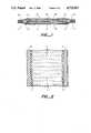
- FIG. 1is a cross section through a first device produced according to the invention
- FIG. 2is a plan view of the device of FIG. 1,
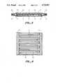
- FIG. 3is a cross section through a second device produced according to the invention, including two layers of PTF inks, and
- FIG. 4is a plan view of the device of FIG. 3.
- the method of the inventionuses a PTF ink in which the solvent for the binder is a latent solvent.
- the inkcan be applied to any substrate, including conventional substrates such as the polyester sheets used in membrane switches. Preferably, however, the ink is applied to a conductive substrate.
- a latent solventmakes it possible to use binders which have not hitherto been used, for example, because at the printing temperature there is either no true solvent for that binder or those solvents that are available are unacceptable for some other reason, for example, because they are toxic, or because they do not have the other desired parameters of the solvent, for example good wettability of the binder material, or because they detrimentally affect the emulsions typically used on the screen in the screen printing technique, or for any combination of those or other reasons.
- a PTF inkcomprising a semicrystalline fluoropolymer (polyvinylidene fluoride) as the binder material.
- PTF inks comprising semicrystalline fluoropolymers as the binder materialare novel per se and form part of the present invention.
- the term "semicrystalline" polymermeans any polymer having at least 5% crystallinity.
- a solventmay be a "true solvent” or a "latent solvent” for that binder.
- the latent solvent selectedis one which wets the binder.
- latent solventsinclude cyclohexanone, butyrolactone, isophorone and carbitol acetate. It is particularly preferred to use isophorone.
- the fillermay have conductive, resistive or insulating properties.
- the selection of the type, quantity and particle size of the filler required to give the desired resultsis well known and well documented in the art.
- the inkis first printed onto the substrate, preferably by screen printing and preferably at room temperature (20° C.). Then the ink is heated to dissolve the binder in the solvent, vaporize the solvent and cure the binder. The vaporization of the solvent (which effectively dries the binder) may alone effect curing of the binder, or the curing may involve a chemical reaction.
- the inkis preferably heated up to, and held at a predetermined temperature, which is hereinafter also referred to as the "cure", temperature, T c .
- T ca predetermined temperature
- the inkis held at that temperature to effect complete vaporization and removal of the solvent and curing of the binder.
- a continuous rate of heatingis used, for example by using an oven.
- the predetermined cure temperature, T c at which the ink is held to vaporize the solvent and cure the inkis preferably at least 15° C., more preferably at least 30° C. above the solvation temperature T s of the binder in the solvent. This is so that substantially complete solvation occurs.
- the predetermined cure temperature, T cmust be lower than the melting point of the substrate, so that the integrity of the substrate is maintained during the curing process.
- the melting point of the substrateis defined as the peak in the curve of a DSC (differential scanning calorimeter) curve.
- the predetermined cure temperature T cis at about the temperature of the onset of melting T om of the substrate, wherein the temperature of the onset of melting is defined as the point of significant increase in slope of the DSC melting curve.
- the vaporization rate of the solventincreases with the temperature up to the boiling point of that solvent. Above the boiling point the vaporization rate is constant.
- the predetermined cure temperature T cis at least 10° C., more preferably at least 30° C. lower than the boiling point of the solvent. This is because the rate of vaporization at the boiling point may be so fast that it causes voiding of the ink film, or a "skin-over" effect, that is trapping of solvent within a cured "skin" of the ink film.
- the boiling point of the solventis above the melting point of the substrate. It is accordingly never reached.
- a polyvinylidene fluoride binderis used with an isophorone solvent, which ink is applied to a polyvinylidene fluoride substrate.
- the solvation temperature of that binder in that solventis 100° C.
- the temperature of the onset of melting and the melting point (as hereinbefore defined) of that substrateare 135° C. and 165° C. respectively, and the boiling point of that solvent is 215° C.
- the predetermined cure temperature, selected to give the optimum rate of vaporization and curingis 135° C.
- the substratecomprises a conductive polymeric material.
- the organic polymer of the ink binderis preferably selected to be a material which has good adhesion to the polymeric component of the conductive polymeric material.
- the polymer component of the conductive polymeric material and the binder of the inkare the same polymer.
- a number of deviceswere prepared by printing PTF inks (both commercially available resistive PTF inks and a resistive ink according to the present invention) onto conductive polymer substrates comprising polyvinylidene fluoride.
- the printingwas in a pattern so as to form electrodes.
- the binder in the ink according to the inventionwas polyvinylidene fluoride. None of the binders in the commercially available inks was polyvinylidene fluoride (since none is available).
- the ink electrodeswere powered and the high temperature resistance stability R n and the voltage stability of the devices were measured. Ageing of the devices, in order to determine the high temperature resistivity of the devices were carried out at 107° C. (225° F.).
- the high temperature resistance stability R nwas computed as the ratio of the resistivity of the device after 1000 hours ageing to its initial resistivity, all resistivity values being measured at 20° C. Ideally that ratio is 1.
- the voltage stabilitywas recorded in terms of the linearity ratio (LR) which is the ratio of the resistance at a low voltage (typically 30 mV) to the resistance at a high voltage (typically 100 V). Ideally that ratio is 1.
- LRlinearity ratio
- the linearity ratiowas measured after 1000 hours of current passage through the device. The results are shown in table 1 below, in which inks Samples Nos. 1 to 8 are commercially available inks and ink Sample No. 9 is an ink according to the present invention.
- vinylis understood to include any polymer blends of polyvinylidene and vinyl acetate.
- a typical vinylcomprises 95% by weight polyvinylchloride and 5% vinylacetate.
- the binderis preferably thermally stable so that it does not shrink or degrade during the ageing process.
- the acrylic/vinyl and polyester/vinyl binders(Samples 2 and 7), for example have poor thermal stability. This is thought to account for their poor electrical behavior in the above tests.
- any suitable materialmay be used for the substrate and for the ink binder.
- materials that may be used theremay be mentioned polyolefins and fluoropolymers.
- polyolefins and fluoropolymersfor some applications, for example where the ink printed substrate is to be used as a heating device, or as part of a heating device, it is desirable that the materials selected have good thermal stability.
- fluoropolymersare preferably used.
- polyvinylidene fluorideis used.
- the fluoropolymeris a semicrystalline polymer.
- the substratein devices in which the substrate is a conductive polymer, the substrate preferably has a resistivity at 23° C. of at least 0.5 ohm.cm, more preferably in the range 0.5 to 100,000 ohm.cm.
- Such devicesmay be used for example as heating devices, with the conductive polymer providing a resistive heating element.
- the conductive and resistive PTF inksmay be used in heating devices.
- the conductive PTF inkspreferably have a resistivity in the range 1 ⁇ 10 -5 to 1 ⁇ 10 -2 ohm.cm, more preferably in the range 1 ⁇ 10 -4 to 1 ⁇ 10 -3 ohm.cm, and contain silver as the predominant filler.
- Such inksmay be used, for example, as electrodes for heating devices, the PTF ink electrodes being printed on a surface of the resistive substrate such that they conduct electric current from a bus bar to the surface of the resistive element.
- the heaters and printed electrodesare as described in copending commonly assigned patent application U.S. Ser. No.
- the resistive PTF inkspreferably have a resistivity in the range 0.5 ⁇ 10 -2 to 10 ohm.cm, and contain carbon as the predominant filler. Such inks may be used in heating devices as an intermediate resistivity layer between the more conductive electrodes and the less conductive resistive substrate. The resistive ink layer improves the electrical contact between the electrodes and the resistive substrate.
- Such an application for the inkis described in copending commonly assigned patent application U.S. Ser. No. 735,408 (MP0961-US3 Batliwalla et al), abandoned, the disclosure of which is incorporated herein by reference.
- a further layeris bonded to the substrate after the ink has been printed onto the substrate.
- the further layermay comprises a dielectric layer bonded to the substrate to improve the physical and electrical properties of the heater.
- a heater incorporating a dielectric layeris disclosed in copending and commonly assigned patent application U.S. Ser. No. 735,409 (Batliwalla et al, MP1062-US1) abandoned, the disclosure of which is incorporated herein by reference.
- the substrateIn order for the device to function as a heater, or to allow deposition onto the substrate of a further layer, it is desirable for the substrate to have good physical and electrical properties.
- a further layeris bonded to the substrate it can affect the physical and/or electrical contact between the ink and the substrate.
- a further layeris used over a conductive substrate, it is particularly preferred that the polymeric component of the conductive polymer substrate is the same as the polymer component of the binder. This is shown by the following comparative test.
- Example Nos. 10 and 11Two devices (Sample Nos. 10 and 11) were prepared, similar to Samples 8 and 9 described above, but including a silicone dielectric layer bonded to the polyvinylidene fluoride (Kynar) substrate in the manner described in the above mentioned copending, commonly assigned application U.S. Ser. No. 735,409 (Batliwalla et al, MP1062-US1).
- the linearity ratio LR measured at 20° C.(after ageing for 1000 hrs. at 107° C. (225° F.)) was measured, and compared to that without the dielectric layer.
- Table 2The results are set out in Table 2 below.
- the ink with the polyvinylidene fluoride (Kynar) binderprovides a device with an acceptable linearity ratio.
- the Figuresillustrate a heater comprising a laminar conductive polymer resistive element 2 having a conductive PTF ink printed on the top surface thereof in the form of interdigitated electrodes 4 and 6.
- the inkcomprises a polyvinylidene fluoride binder containing a functional phase or filler of silver, graphite and carbon black particles.
- the inkBefore application to the device the ink also comprises an isophorone solvent which at room temperature is a latent solvent for the binder.
- the inkis applied to the resistive element 2 by first screen printing the ink on the element at room temperature, then raising the temperature to dissolve the binder in the solvent, then further raising the temperature to vaporize the solvent and cure the binder.
- a dielectric layer 8overlies the interdigitating portions of the electrodes but does not extend to the longitudinal margins of the electrodes.
- Bus bars 10 and 12extend along the longitudinal margins of the electrodes.
- An insulating jacket(shown in FIG. 1 only) is formed around the heating element, and bus bars by a polymeric bottom sheet 14 and a polymeric top sheet 16.
- Sheet 14is secured to the bottom of the heating element 2, and to the edge portions of the top sheet by a substantially continuous layer of adhesive 17 (as shown), or by melt bonding (not shown).
- the top sheet 16is adjacent to but not secured to the bus bars 10 and 12, the dielectric 8, the electrodes 4 and 6, or the resistive element 2.
- FIGS. 3 and 4show a heater similar to that shown in FIGS. 1 and 2 comprising a laminar conductive polymer resistive element 2.
- Printed on the top surface of the resistive element 2is an interdigitated pattern of a resistive ink 30 which contains carbon black, or a mixture of graphite and carbon black, as the conductive filler, and has substantially lower resistivity than the conductive polymer in the element 2.
- Printed over the resistive ink 30are interdigitated electrodes 32 which are composed of a conductive PTF ink containing a metal filler e.g. silver, as the conductive filler and having lower resistivity than the conductive polymer in the resistive pattern 30.
- the configuration of the electrodes 32is identical to that of the underprint layer 30, but the electrodes are narrower than the underprint layer. Thus the layer 30 extends between the electrodes 32 and the resistive element 2, and extends slightly beyond the electrodes 32.
- Bus bars 10 and 12, as used in the device of FIGS. 1 and 2are provided.
- An insulating jacket in the form of a polymeric bottom sheet 14 and a polymer top sheet 16 which is secured by adhesive 17 or by a melt bond,is also provided as in the device illustrated in FIGS. 1 and 2, as is a metallic foil 18 which is held in place by polymeric insulating sheet 20 secured to sheet 18 by adhesive layers 22 and 23 or by a melt bond.
- a conductive PTF ink having a resistivity of 1 ⁇ 10 -3 ohm.cmwas prepared, having the following composition:
- the conductive inkmay be used, for example as the electrodes 4 and 6 in the heater described with reference to FIGS. 1 and 2, or as the electrodes 32 in the heater described with reference to FIGS. 3 and 4.
- a resistive PTF ink having a resistivity of 0.2 ohm.cmwas prepared having the following composition.
- the resistive inkmay be used, for example as the intermediate resistivity layer 30 in the heater described with references to FIGS. 3 and 4.
- the conductive and resistive inks detailed abovemay be prepared by the following method.
- the blendis placed in a 3-roll paint mill in which there is a 28 mm gap between the feed and outer rollers, and in which there is no contact between the take-off and central rollers.
- the remaining Cab-O-Silis added to the mill and the blend milled for 45 minutes.
- the inkis removed from the mill by adjusting the position of the take-off roller, and additional solvent added, if required, to give the required viscosity for screen printing.
Landscapes
- Chemical & Material Sciences (AREA)
- Engineering & Computer Science (AREA)
- Physics & Mathematics (AREA)
- Dispersion Chemistry (AREA)
- Spectroscopy & Molecular Physics (AREA)
- Life Sciences & Earth Sciences (AREA)
- Materials Engineering (AREA)
- Wood Science & Technology (AREA)
- Organic Chemistry (AREA)
- Manufacturing & Machinery (AREA)
- Microelectronics & Electronic Packaging (AREA)
- Inks, Pencil-Leads, Or Crayons (AREA)
Abstract
Description
TABLE 1 ______________________________________ Sample 1000 1000 hr. No. Ink Binder hr Rn Linearity Ratio ______________________________________ (1) 5524228 Urethane >20.0 >18.0 Supplied by Acheson (2) 41755 acrylic & vinyl >20.0 >36.0 Supplied by Acheson (3) 5030-7 epoxy >20.0 >40.0 Supplied by Amican (4) 1111-S epoxy 2.10 1.102 Supplied by E.S.L. (5) SS24302 Viton 1.95 2.69 Supplied by Acheson (6) 504SS Viton 2.00 1.026 Supplied by Acheson (7) 426SS polyester & vinyl 2.01 1.087 Supplied by Acheson (8) SS24360 vinyl 1.39 1.003 Supplied by Acheson (9) GM11 Kynar PVF.sub.2 1.20 1.002 ______________________________________
TABLE 2 ______________________________________ 1000 hr L.R. 1000 hr L.R. without with Sample dielectric dielectric No. Ink Binder layer layer ______________________________________ (10) SS24360 vinyl 1.003 1.036 Supplied by Acheson (11) polyvinylidene fluoride 1.002 1.003 (Kynar) ______________________________________
______________________________________ wt % ______________________________________ Kynar 461, (binder) 19.3 Silver Flake 11401 43.1 (filler) (10 m diameter size) Graphite 870 (filler) 6.3 Carbon black XC72 (filler) 1.8 Cab-O-Sil M5 1.8 Isophorone (solvent) 27.7 ______________________________________ Silver Flake 11401 supplied by Aesar, Johnson Mathey U.S.A. Kynar 461 is a polyvinylidene fluoride supplied by Pennwalt U.S.A. Graphite 870 is supplied by Ashbury Graphite. Carbon black XC72 is supplied by Cabot. CabO-Sil is a fumed silica supplied by Cabot.
______________________________________ wt % ______________________________________ Kynar 461 (binder) 14.5 Graphite 870 (filler) 32.9 Carbon Black XC72 (filler) 2.2 Cab-O-Sil 0.7 Isphorone (solvent) 49.7 ______________________________________
Claims (12)
Priority Applications (7)
| Application Number | Priority Date | Filing Date | Title |
|---|---|---|---|
| US06/764,894US4722853A (en) | 1985-08-12 | 1985-08-12 | Method of printing a polymer thick film ink |
| DE8686306198TDE3669007D1 (en) | 1985-08-12 | 1986-08-11 | POLYMER THICK FILM INKS. |
| JP61189480AJPH0816204B2 (en) | 1985-08-12 | 1986-08-11 | Method for forming a conductive layer from polymer thick film ink |
| IN643/MAS/86AIN167878B (en) | 1985-08-12 | 1986-08-11 | |
| AT86306198TATE50376T1 (en) | 1985-08-12 | 1986-08-11 | POLYMER THICK COAT INKS. |
| CA000515653ACA1277829C (en) | 1985-08-12 | 1986-08-11 | Polymer thick film inks |
| EP86306198AEP0217512B1 (en) | 1985-08-12 | 1986-08-11 | Polymer thick film inks |
Applications Claiming Priority (1)
| Application Number | Priority Date | Filing Date | Title |
|---|---|---|---|
| US06/764,894US4722853A (en) | 1985-08-12 | 1985-08-12 | Method of printing a polymer thick film ink |
Publications (1)
| Publication Number | Publication Date |
|---|---|
| US4722853Atrue US4722853A (en) | 1988-02-02 |
Family
ID=25072090
Family Applications (1)
| Application Number | Title | Priority Date | Filing Date |
|---|---|---|---|
| US06/764,894Expired - LifetimeUS4722853A (en) | 1985-08-12 | 1985-08-12 | Method of printing a polymer thick film ink |
Country Status (7)
| Country | Link |
|---|---|
| US (1) | US4722853A (en) |
| EP (1) | EP0217512B1 (en) |
| JP (1) | JPH0816204B2 (en) |
| AT (1) | ATE50376T1 (en) |
| CA (1) | CA1277829C (en) |
| DE (1) | DE3669007D1 (en) |
| IN (1) | IN167878B (en) |
Cited By (25)
| Publication number | Priority date | Publication date | Assignee | Title |
|---|---|---|---|---|
| US5093036A (en)* | 1988-09-20 | 1992-03-03 | Raychem Corporation | Conductive polymer composition |
| US5181006A (en)* | 1988-09-20 | 1993-01-19 | Raychem Corporation | Method of making an electrical device comprising a conductive polymer composition |
| WO1998053311A3 (en)* | 1997-05-23 | 1999-02-18 | Gamera Bioscience Corp | Devices and methods for using centripetal acceleration to drive fluid movement in a microfluidics system |
| US5932643A (en)* | 1997-04-11 | 1999-08-03 | Ncr Corporation | Thermal transfer ribbon with conductive polymers |
| US6121585A (en)* | 1999-03-30 | 2000-09-19 | Robert Dam | Electrically heated beverage cup and cupholder system |
| US6143247A (en)* | 1996-12-20 | 2000-11-07 | Gamera Bioscience Inc. | Affinity binding-based system for detecting particulates in a fluid |
| US6143248A (en)* | 1996-08-12 | 2000-11-07 | Gamera Bioscience Corp. | Capillary microvalve |
| US20020088788A1 (en)* | 1998-03-26 | 2002-07-11 | Wesco, Inc. | Thermal warming garments for user temperature management |
| US20020128333A1 (en)* | 2000-06-20 | 2002-09-12 | Tang Ho Yin | Low switching temperature polymer positive temperature coefficient device |
| US6554940B2 (en) | 1997-06-03 | 2003-04-29 | Cubic Co., Ltd. | Method of transferring a print pattern composed of a fluoropolymer resin and an inorganic pigment onto an objective body using liquid pressure |
| US6632399B1 (en) | 1998-05-22 | 2003-10-14 | Tecan Trading Ag | Devices and methods for using centripetal acceleration to drive fluid movement in a microfluidics system for performing biological fluid assays |
| US20030232403A1 (en)* | 1999-06-18 | 2003-12-18 | Kellogg Gregory L. | Devices and methods for the performance of miniaturized homogeneous assays |
| US20040026033A1 (en)* | 2000-04-04 | 2004-02-12 | Price David M. | High speed flip chip assembly process |
| US20040038647A1 (en)* | 1993-12-20 | 2004-02-26 | Intermec Technologies Corporation | Local area network having multiple channel wireless access |
| US20040212951A1 (en)* | 1999-05-24 | 2004-10-28 | Showa Denko K.K. | Solid electrolytic capacitor and method for producing the same |
| EP1538637A1 (en)* | 2003-12-04 | 2005-06-08 | E. I. du Pont de Nemours and Company | Conductor compositions |
| US20050121653A1 (en)* | 2003-12-08 | 2005-06-09 | Chacko Antony P. | Polymer conductive composition containing zirconia for films and coatings with high wear resistance |
| WO2005039240A3 (en)* | 2003-10-16 | 2005-07-14 | Christian Hug | Device for heating by means of a heating flexible film and the use of said device for protecting cultures and plants against cold damage |
| EP1696006A1 (en)* | 2005-02-28 | 2006-08-30 | Samsung SDI Germany GmbH | metal ink and substrate for a display and method for manufacturing the same |
| US20060192183A1 (en)* | 2005-02-28 | 2006-08-31 | Andreas Klyszcz | Metal ink, method of preparing the metal ink, substrate for display, and method of manufacturing the substrate |
| US20080073594A1 (en)* | 2006-05-11 | 2008-03-27 | Chyi-Ran Lee | Infrared ray generator |
| US20080179306A1 (en)* | 2002-11-21 | 2008-07-31 | W.E.T. Automotives Systems Ag | Heater for automotive vehicle and method of forming same |
| US20100069553A1 (en)* | 2008-09-18 | 2010-03-18 | Eastman Chemical Company | Polyester melt-phase compositions having improved thermo-oxidative stability, and methods of making and using them |
| US8360239B2 (en) | 2010-02-15 | 2013-01-29 | Kroell Keith B | Kit for transferring an image onto an object |
| CN104813425A (en)* | 2012-10-17 | 2015-07-29 | 新加坡科技设计大学 | High specific capacitance and high power density of printed flexible micro-supercapacitors |
Families Citing this family (2)
| Publication number | Priority date | Publication date | Assignee | Title |
|---|---|---|---|---|
| SG87047A1 (en)* | 1998-08-31 | 2002-03-19 | Dainippon Ink & Chemicals | Conductive sheet, process for producing the same, and molded article |
| KR102010610B1 (en)* | 2011-09-09 | 2019-08-13 | 더 케무어스 컴퍼니 에프씨, 엘엘씨 | An ink composition for a non-stick coating and a coated substrate comprising the pattern therefrom |
Citations (7)
| Publication number | Priority date | Publication date | Assignee | Title |
|---|---|---|---|---|
| US3331823A (en)* | 1963-04-01 | 1967-07-18 | Montedison Spa | Copolymers of vinylidene fluoride with 1, 2, 3, 3, 3-pentafluoropropylene |
| FR2098273A1 (en)* | 1970-07-09 | 1972-03-10 | Ericsson Telefon Ab L M | Electric cables - with semiconducting layer applied from aqs compsn contg carbon black and dispersed polyethylene |
| US3993842A (en)* | 1973-04-24 | 1976-11-23 | E. I. Du Pont De Nemours And Company | Electrically conductive elastomeric ink |
| FR2419570A1 (en)* | 1978-03-10 | 1979-10-05 | Reuter Technologie Gmbh | Electroconductive plastics layers prodn. - by mixing aq. plastics latex with aq. dispersion of conductive particles and drying film of the mixt. at above the m.pt. of the resin |
| EP0074281A1 (en)* | 1981-09-09 | 1983-03-16 | RAYCHEM CORPORATION (a Delaware corporation) | Heating Diesel fuel |
| US4479890A (en)* | 1982-10-05 | 1984-10-30 | Rca Corporation | Thick film resistor inks |
| EP0158410A1 (en)* | 1984-01-23 | 1985-10-16 | RAYCHEM CORPORATION (a Delaware corporation) | Laminar Conductive polymer devices |
Family Cites Families (2)
| Publication number | Priority date | Publication date | Assignee | Title |
|---|---|---|---|---|
| JPS5710148A (en)* | 1980-06-20 | 1982-01-19 | Fuji Photo Film Co Ltd | Electrophotographic receptor |
| CA1173644A (en)* | 1981-07-06 | 1984-09-04 | Ashok N. Prabhu | Air-fireable thick film inks |
- 1985
- 1985-08-12USUS06/764,894patent/US4722853A/ennot_activeExpired - Lifetime
- 1986
- 1986-08-11ININ643/MAS/86Apatent/IN167878B/enunknown
- 1986-08-11EPEP86306198Apatent/EP0217512B1/ennot_activeExpired - Lifetime
- 1986-08-11DEDE8686306198Tpatent/DE3669007D1/ennot_activeExpired - Fee Related
- 1986-08-11CACA000515653Apatent/CA1277829C/ennot_activeExpired - Lifetime
- 1986-08-11ATAT86306198Tpatent/ATE50376T1/enactive
- 1986-08-11JPJP61189480Apatent/JPH0816204B2/ennot_activeExpired - Fee Related
Patent Citations (7)
| Publication number | Priority date | Publication date | Assignee | Title |
|---|---|---|---|---|
| US3331823A (en)* | 1963-04-01 | 1967-07-18 | Montedison Spa | Copolymers of vinylidene fluoride with 1, 2, 3, 3, 3-pentafluoropropylene |
| FR2098273A1 (en)* | 1970-07-09 | 1972-03-10 | Ericsson Telefon Ab L M | Electric cables - with semiconducting layer applied from aqs compsn contg carbon black and dispersed polyethylene |
| US3993842A (en)* | 1973-04-24 | 1976-11-23 | E. I. Du Pont De Nemours And Company | Electrically conductive elastomeric ink |
| FR2419570A1 (en)* | 1978-03-10 | 1979-10-05 | Reuter Technologie Gmbh | Electroconductive plastics layers prodn. - by mixing aq. plastics latex with aq. dispersion of conductive particles and drying film of the mixt. at above the m.pt. of the resin |
| EP0074281A1 (en)* | 1981-09-09 | 1983-03-16 | RAYCHEM CORPORATION (a Delaware corporation) | Heating Diesel fuel |
| US4479890A (en)* | 1982-10-05 | 1984-10-30 | Rca Corporation | Thick film resistor inks |
| EP0158410A1 (en)* | 1984-01-23 | 1985-10-16 | RAYCHEM CORPORATION (a Delaware corporation) | Laminar Conductive polymer devices |
Cited By (39)
| Publication number | Priority date | Publication date | Assignee | Title |
|---|---|---|---|---|
| US5181006A (en)* | 1988-09-20 | 1993-01-19 | Raychem Corporation | Method of making an electrical device comprising a conductive polymer composition |
| US5093036A (en)* | 1988-09-20 | 1992-03-03 | Raychem Corporation | Conductive polymer composition |
| US20040038647A1 (en)* | 1993-12-20 | 2004-02-26 | Intermec Technologies Corporation | Local area network having multiple channel wireless access |
| US6143248A (en)* | 1996-08-12 | 2000-11-07 | Gamera Bioscience Corp. | Capillary microvalve |
| US6143247A (en)* | 1996-12-20 | 2000-11-07 | Gamera Bioscience Inc. | Affinity binding-based system for detecting particulates in a fluid |
| US5932643A (en)* | 1997-04-11 | 1999-08-03 | Ncr Corporation | Thermal transfer ribbon with conductive polymers |
| US6548788B2 (en) | 1997-05-23 | 2003-04-15 | Tecan Trading Ag | Devices and methods for using centripetal acceleration to drive fluid movement in a microfluidics system |
| WO1998053311A3 (en)* | 1997-05-23 | 1999-02-18 | Gamera Bioscience Corp | Devices and methods for using centripetal acceleration to drive fluid movement in a microfluidics system |
| US20040089616A1 (en)* | 1997-05-23 | 2004-05-13 | Gregory Kellogg | Devices and methods for using centripetal acceleration to drive fluid movement in a microfluidics system for performing biological fluid assays |
| US6399361B2 (en) | 1997-05-23 | 2002-06-04 | Tecan Trading Ag | Devices and methods for using centripetal acceleration to drive fluid movement in a microfluidics system |
| US6852394B2 (en) | 1997-06-03 | 2005-02-08 | Cubic Co., Ltd | Liquid pressure pattern-transferring ink, a liquid pressure pattern-transferring film, a liquid pressure patttern-transferred article and a method of transferring a print pattern on an objective body under a liquid pressure |
| US6554940B2 (en) | 1997-06-03 | 2003-04-29 | Cubic Co., Ltd. | Method of transferring a print pattern composed of a fluoropolymer resin and an inorganic pigment onto an objective body using liquid pressure |
| US20030121598A1 (en)* | 1997-06-03 | 2003-07-03 | Nobuyuki Otaki | Liquid pressure pattern-transferring ink, a liquid pressure pattern-transferring film, a liquid pressure pattern-transferred article and a method of transferring a print pattern on an objective body under a liquid pressure |
| US20020088788A1 (en)* | 1998-03-26 | 2002-07-11 | Wesco, Inc. | Thermal warming garments for user temperature management |
| US6632399B1 (en) | 1998-05-22 | 2003-10-14 | Tecan Trading Ag | Devices and methods for using centripetal acceleration to drive fluid movement in a microfluidics system for performing biological fluid assays |
| US6121585A (en)* | 1999-03-30 | 2000-09-19 | Robert Dam | Electrically heated beverage cup and cupholder system |
| US7060205B2 (en)* | 1999-05-24 | 2006-06-13 | Showa Denko Kabushiki Kaisha | Solid electrolytic capacitor and method for producing the same |
| US20040212951A1 (en)* | 1999-05-24 | 2004-10-28 | Showa Denko K.K. | Solid electrolytic capacitor and method for producing the same |
| US20030232403A1 (en)* | 1999-06-18 | 2003-12-18 | Kellogg Gregory L. | Devices and methods for the performance of miniaturized homogeneous assays |
| US20040026033A1 (en)* | 2000-04-04 | 2004-02-12 | Price David M. | High speed flip chip assembly process |
| US20020128333A1 (en)* | 2000-06-20 | 2002-09-12 | Tang Ho Yin | Low switching temperature polymer positive temperature coefficient device |
| US7741582B2 (en) | 2002-11-21 | 2010-06-22 | W.E.T. Automotive Systems Ag | Heater for automotive vehicle and method of forming same |
| US9578690B2 (en) | 2002-11-21 | 2017-02-21 | Gentherm Gmbh | Heater for an automotive vehicle and method of forming same |
| US9315133B2 (en) | 2002-11-21 | 2016-04-19 | Gentherm Gmbh | Heater for an automotive vehicle and method of forming same |
| US20080179306A1 (en)* | 2002-11-21 | 2008-07-31 | W.E.T. Automotives Systems Ag | Heater for automotive vehicle and method of forming same |
| US8766142B2 (en) | 2002-11-21 | 2014-07-01 | W.E.T. Automotive Systems Ag | Heater for an automotive vehicle and method of forming same |
| US8507831B2 (en) | 2002-11-21 | 2013-08-13 | W.E.T. Automotive Systems Ag | Heater for an automotive vehicle and method of forming same |
| WO2005039240A3 (en)* | 2003-10-16 | 2005-07-14 | Christian Hug | Device for heating by means of a heating flexible film and the use of said device for protecting cultures and plants against cold damage |
| EP1538637A1 (en)* | 2003-12-04 | 2005-06-08 | E. I. du Pont de Nemours and Company | Conductor compositions |
| US20050121653A1 (en)* | 2003-12-08 | 2005-06-09 | Chacko Antony P. | Polymer conductive composition containing zirconia for films and coatings with high wear resistance |
| US7141184B2 (en)* | 2003-12-08 | 2006-11-28 | Cts Corporation | Polymer conductive composition containing zirconia for films and coatings with high wear resistance |
| US20060192183A1 (en)* | 2005-02-28 | 2006-08-31 | Andreas Klyszcz | Metal ink, method of preparing the metal ink, substrate for display, and method of manufacturing the substrate |
| EP1696006A1 (en)* | 2005-02-28 | 2006-08-30 | Samsung SDI Germany GmbH | metal ink and substrate for a display and method for manufacturing the same |
| US7511291B2 (en)* | 2006-05-11 | 2009-03-31 | Ws Far Ir Medical Technology Co., Ltd. | Infrared ray generator |
| US20080073594A1 (en)* | 2006-05-11 | 2008-03-27 | Chyi-Ran Lee | Infrared ray generator |
| US20100069553A1 (en)* | 2008-09-18 | 2010-03-18 | Eastman Chemical Company | Polyester melt-phase compositions having improved thermo-oxidative stability, and methods of making and using them |
| US8360239B2 (en) | 2010-02-15 | 2013-01-29 | Kroell Keith B | Kit for transferring an image onto an object |
| CN104813425A (en)* | 2012-10-17 | 2015-07-29 | 新加坡科技设计大学 | High specific capacitance and high power density of printed flexible micro-supercapacitors |
| US9824828B2 (en) | 2012-10-17 | 2017-11-21 | Singapore University Of Technology And Design | High specific capacitance and high power density of printed flexible micro-supercapacitors |
Also Published As
| Publication number | Publication date |
|---|---|
| JPS6239678A (en) | 1987-02-20 |
| ATE50376T1 (en) | 1990-02-15 |
| JPH0816204B2 (en) | 1996-02-21 |
| IN167878B (en) | 1991-01-05 |
| EP0217512B1 (en) | 1990-02-07 |
| DE3669007D1 (en) | 1990-03-15 |
| EP0217512A1 (en) | 1987-04-08 |
| CA1277829C (en) | 1990-12-18 |
Similar Documents
| Publication | Publication Date | Title |
|---|---|---|
| US4722853A (en) | Method of printing a polymer thick film ink | |
| US5181006A (en) | Method of making an electrical device comprising a conductive polymer composition | |
| DE3854498T2 (en) | Electrical device with a resistance element made of PTC polymer. | |
| US5093036A (en) | Conductive polymer composition | |
| US4980541A (en) | Conductive polymer composition | |
| JP3558771B2 (en) | Positive temperature coefficient composition | |
| EP0918339A2 (en) | Electrical device containing positive temperature coefficient resistor composition and method of manufacturing the device | |
| KR19980703168A (en) | Conductive Polymer Compositions and Devices | |
| US5677662A (en) | Heat-sensitive resistive compound and method for producing it and using it | |
| EP0435923B1 (en) | Conductive polymer composition | |
| EP0176284B1 (en) | Electrical contact between metals of different resistivities | |
| CA1133085A (en) | Temperature sensitive electrical device | |
| CA1251509A (en) | Making electrical contact between metals and resistive elements | |
| HK1021613B (en) | Conductive polymer composition | |
| HK1028480A (en) | Conductive polymer composition | |
| MXPA98009261A (en) | Electrical device containing a composition of positive temperature coefficient resistor and method for manufacturing the disposit |
Legal Events
| Date | Code | Title | Description |
|---|---|---|---|
| AS | Assignment | Owner name:RAYCHEM CORPORATION, 300 CONSTITUTION DRIVE, MENLO Free format text:ASSIGNMENT OF ASSIGNORS INTEREST.;ASSIGNORS:BATLIWALLA, NEVILLE;OSWAL, RAVI;MC CARTY, GORDON;AND OTHERS;REEL/FRAME:004443/0530 Effective date:19850812 | |
| STCF | Information on status: patent grant | Free format text:PATENTED CASE | |
| FPAY | Fee payment | Year of fee payment:4 | |
| FPAY | Fee payment | Year of fee payment:8 | |
| FPAY | Fee payment | Year of fee payment:12 | |
| AS | Assignment | Owner name:TYCO ELECTRONICS CORPORATION, PENNSYLVANIA Free format text:CHANGE OF NAME;ASSIGNOR:AMP INCORPORATED;REEL/FRAME:011682/0568 Effective date:19990913 Owner name:TYCO INTERNATIONAL (PA), INC., NEW HAMPSHIRE Free format text:MERGER & REORGANIZATION;ASSIGNOR:RAYCHEM CORPORATION;REEL/FRAME:011682/0608 Effective date:19990812 Owner name:TYCO INTERNATIONAL LTD., BERMUDA Free format text:MERGER & REORGANIZATION;ASSIGNOR:RAYCHEM CORPORATION;REEL/FRAME:011682/0608 Effective date:19990812 Owner name:AMP INCORPORATED, PENNSYLVANIA Free format text:MERGER & REORGANIZATION;ASSIGNOR:RAYCHEM CORPORATION;REEL/FRAME:011682/0608 Effective date:19990812 |