US4719615A - Erasable optical data storage medium - Google Patents
Erasable optical data storage mediumDownload PDFInfo
- Publication number
- US4719615A US4719615AUS06/835,960US83596086AUS4719615AUS 4719615 AUS4719615 AUS 4719615AUS 83596086 AUS83596086 AUS 83596086AUS 4719615 AUS4719615 AUS 4719615A
- Authority
- US
- United States
- Prior art keywords
- medium
- layer
- data
- light
- optically
- Prior art date
- Legal status (The legal status is an assumption and is not a legal conclusion. Google has not performed a legal analysis and makes no representation as to the accuracy of the status listed.)
- Expired - Lifetime
Links
Images


Classifications
- G—PHYSICS
- G11—INFORMATION STORAGE
- G11B—INFORMATION STORAGE BASED ON RELATIVE MOVEMENT BETWEEN RECORD CARRIER AND TRANSDUCER
- G11B7/00—Recording or reproducing by optical means, e.g. recording using a thermal beam of optical radiation by modifying optical properties or the physical structure, reproducing using an optical beam at lower power by sensing optical properties; Record carriers therefor
- G11B7/24—Record carriers characterised by shape, structure or physical properties, or by the selection of the material
- G11B7/241—Record carriers characterised by shape, structure or physical properties, or by the selection of the material characterised by the selection of the material
- G11B7/242—Record carriers characterised by shape, structure or physical properties, or by the selection of the material characterised by the selection of the material of recording layers
- G11B7/244—Record carriers characterised by shape, structure or physical properties, or by the selection of the material characterised by the selection of the material of recording layers comprising organic materials only
- G11B7/245—Record carriers characterised by shape, structure or physical properties, or by the selection of the material characterised by the selection of the material of recording layers comprising organic materials only containing a polymeric component
- G—PHYSICS
- G11—INFORMATION STORAGE
- G11B—INFORMATION STORAGE BASED ON RELATIVE MOVEMENT BETWEEN RECORD CARRIER AND TRANSDUCER
- G11B7/00—Recording or reproducing by optical means, e.g. recording using a thermal beam of optical radiation by modifying optical properties or the physical structure, reproducing using an optical beam at lower power by sensing optical properties; Record carriers therefor
- G11B7/004—Recording, reproducing or erasing methods; Read, write or erase circuits therefor
- G11B7/0045—Recording
- G11B7/00452—Recording involving bubble or bump forming
- G—PHYSICS
- G11—INFORMATION STORAGE
- G11B—INFORMATION STORAGE BASED ON RELATIVE MOVEMENT BETWEEN RECORD CARRIER AND TRANSDUCER
- G11B7/00—Recording or reproducing by optical means, e.g. recording using a thermal beam of optical radiation by modifying optical properties or the physical structure, reproducing using an optical beam at lower power by sensing optical properties; Record carriers therefor
- G11B7/004—Recording, reproducing or erasing methods; Read, write or erase circuits therefor
- G11B7/0055—Erasing
- G—PHYSICS
- G11—INFORMATION STORAGE
- G11B—INFORMATION STORAGE BASED ON RELATIVE MOVEMENT BETWEEN RECORD CARRIER AND TRANSDUCER
- G11B7/00—Recording or reproducing by optical means, e.g. recording using a thermal beam of optical radiation by modifying optical properties or the physical structure, reproducing using an optical beam at lower power by sensing optical properties; Record carriers therefor
- G11B7/24—Record carriers characterised by shape, structure or physical properties, or by the selection of the material
- G11B7/241—Record carriers characterised by shape, structure or physical properties, or by the selection of the material characterised by the selection of the material
- G11B7/242—Record carriers characterised by shape, structure or physical properties, or by the selection of the material characterised by the selection of the material of recording layers
- G11B7/244—Record carriers characterised by shape, structure or physical properties, or by the selection of the material characterised by the selection of the material of recording layers comprising organic materials only
- G11B7/246—Record carriers characterised by shape, structure or physical properties, or by the selection of the material characterised by the selection of the material of recording layers comprising organic materials only containing dyes
- G11B7/2467—Record carriers characterised by shape, structure or physical properties, or by the selection of the material characterised by the selection of the material of recording layers comprising organic materials only containing dyes azo-dyes
- G—PHYSICS
- G11—INFORMATION STORAGE
- G11B—INFORMATION STORAGE BASED ON RELATIVE MOVEMENT BETWEEN RECORD CARRIER AND TRANSDUCER
- G11B7/00—Recording or reproducing by optical means, e.g. recording using a thermal beam of optical radiation by modifying optical properties or the physical structure, reproducing using an optical beam at lower power by sensing optical properties; Record carriers therefor
- G11B7/24—Record carriers characterised by shape, structure or physical properties, or by the selection of the material
- G11B7/241—Record carriers characterised by shape, structure or physical properties, or by the selection of the material characterised by the selection of the material
- G11B7/242—Record carriers characterised by shape, structure or physical properties, or by the selection of the material characterised by the selection of the material of recording layers
- G11B7/244—Record carriers characterised by shape, structure or physical properties, or by the selection of the material characterised by the selection of the material of recording layers comprising organic materials only
- G11B7/246—Record carriers characterised by shape, structure or physical properties, or by the selection of the material characterised by the selection of the material of recording layers comprising organic materials only containing dyes
- G11B7/248—Record carriers characterised by shape, structure or physical properties, or by the selection of the material characterised by the selection of the material of recording layers comprising organic materials only containing dyes porphines; azaporphines, e.g. phthalocyanines
- G—PHYSICS
- G11—INFORMATION STORAGE
- G11B—INFORMATION STORAGE BASED ON RELATIVE MOVEMENT BETWEEN RECORD CARRIER AND TRANSDUCER
- G11B7/00—Recording or reproducing by optical means, e.g. recording using a thermal beam of optical radiation by modifying optical properties or the physical structure, reproducing using an optical beam at lower power by sensing optical properties; Record carriers therefor
- G11B7/24—Record carriers characterised by shape, structure or physical properties, or by the selection of the material
- G11B7/241—Record carriers characterised by shape, structure or physical properties, or by the selection of the material characterised by the selection of the material
- G11B7/252—Record carriers characterised by shape, structure or physical properties, or by the selection of the material characterised by the selection of the material of layers other than recording layers
- G11B7/253—Record carriers characterised by shape, structure or physical properties, or by the selection of the material characterised by the selection of the material of layers other than recording layers of substrates
- G11B7/2532—Record carriers characterised by shape, structure or physical properties, or by the selection of the material characterised by the selection of the material of layers other than recording layers of substrates comprising metals
Definitions
- the present inventionrelates generally to a data storage medium and methods and apparatus for recording data on the medium, and, more particularly, to an erasable optical data storage medium and methods and apparatus for writing, erasing, and reading data on the data storage medium.
- the practical or commercial techniques for recording dataare based substantially on magnetic storage technology.
- the dataare stored on magnetic media, such as discs and tapes, on which logic 1 data bits and logic 0 data bits are represented by the magnetization of a medium.
- magnetic mediasuch as discs and tapes
- logic 1 data bits and logic 0 data bitsare represented by the magnetization of a medium.
- one direction of magnetization of a given location or bit storage area of the data storage mediumcan represent a logic 1
- another direction of magnetization of that bit storage areacan represent a logic 0.
- Each data bitis written on the medium by using a recording head to magnetize the given bit storage area, and each data bit can be erased by writing another bit over the given bit storage area using the magnetic recording head.
- Each data bitis read by using the recording head to sense the magnetization of the given bit area.
- optical recordingpotentially has significant advantages over magnetic recording, including higher data storage density, higher data rates, and longer data archival capabilities.
- One type of optical recording that has the highest potentialis an optical recording apparatus or system which uses, in lieu of the magnetic recording head, a highly focused laser beam as an ultra-fine recording stylus to write and read data at a very high data rate and recording density, and to erase the data.
- the systemincludes an erasable optical data storage medium that responds to the laser beam to store the data.
- the data storage mediumresponds to the heat generated by the laser beam to erase and write the data, and responds to the light of the laser beam to read the data.
- a laser beamis focused on the erasable data storage medium to heat the medium and, thereby, induce a stable transition from one morphological or physical state, e.g., an amorphous state, to another morphological or physical state, to another morphological or physical state, e.g., a crystalline state.
- the two physical stateshave different optical properties which are the optical transmittance and optical reflectance properties of the respective states. Therefore, to read the data bit, light from the laser beam, which is at a lower power level than is used for writing, is focused on the data storage medium and will be transmitted or reflected by the medium depending on the physical state of the medium, thereby representing a logic 1 or logic 0.
- the data bitcan be erased by again heating the material with the laser beam at a higher power level to return the medium to its original physical state.
- the above-mentioned erasable optical data storage mediumis made of semiconductor or chalcogenide materials that, as already stated, change from one state to another when heated.
- One problem with this data storage mediumis that these changes in state are very small or slight, i.e., the amorphous and crystalline states are not substantially distinguishable optically. Therefore, a high signal-to-noise ratio of a reflected laser beam is not obtainable to distinguish between a logic 1 and a logic 0 upon reading the data bit.
- Another problem with this data storage mediumis that the data rate, in particular the writing and erasing speeds, is undesirably very low, e.g., one microsecond.
- U.S. Pat. No. 4,278,734 to Ohta et aldiscloses an optical medium in which the material of the medium changes physical state, leading to an increase or decrease in optical density.
- Ohta et alappears to have solved the data rate problem in that data may be written or erased quickly, e.g. in 50 nsec.
- Ohta et alalso appears to have solved the contrast problem in that the physical states are distinguishable optically.
- one disadvantage of Ohta et alis that the data cannot be erased, bit-by-bit, since a localized bit area location cannot be achieved.
- the physical change of state or transformationcannot occur on a surface which has anomalies or irregularities in the surface.
- the materials used for the optical mediumare expensive.
- U.S. Pat. No. 4,264,986 to Willis, issued Apr. 28, 1981discloses another type or erasable optical data storage medium.
- a laser beamis focused on the medium to induce, by heating, a volumetric expansion of the bit area being heated, thereby creating a small bump or deformation.
- the presence of the bumprepresents one logic state, while the absence of the bump represents the other logic state.
- the bit area of the data storage mediumchanges from one physical state, i.e., crystalline, to another physical state, i.e., amorphous, which is the phenomenon that causes the volumetric expansion, thereby creating the small bump which becomes reversibly fixed.
- a bitis read by focusing on the bit area a laser beam of lower power than is used for writing, and then detecting the amount or scattering of reflected light. If the bump is present, the reflected light will be substantially scattered, so that the intensity of the detected light will be higher.
- This read/write recording methodis attractive, since it provides a good signal-to-noise ratio to distinguish a logic 1 from a logic 0.
- U.S. Pat. No. 4,371,954 to Cornetdiscloses an erasable optical data storage medium including a substrate, having a low coefficient of thermal expansion, which supports a dual layer having a bottom layer of material and a top layer of material.
- the bottom layer of materialis a relatively inextensible metal or polymer having a high coefficient of thermal expansion
- the top layeris a metal alloy which is in a martensitic phase at ambient temperature and has a low coefficient of thermal expansion.
- the bottom layer and top layerhave a low adhesion to one another, i.e., they are not bonded together, and the latter has a transformation temperature T t above ambient and below the melting point of the former layer. Above the transformation temperature T t , the top layer is in its "parent" phase.
- a light pulse from a laser beamis absorbed by the dual layer, resulting in the heating of the dual layer at a temperature below the transformation temperature T t , as well as a differential expansion between the two layers.
- the bottom layerdelaminates or disengages from the substrate and volumetrically expands onto the top layer which forms a bump.
- the top layerforms a reversibly fixed bump and the bottom layer contracts back onto the substrate.
- the martensitic top layeris raised to a temperature exceeding the transformation temperature T t , either by, for example, a higher power laser pulse or a slower displacement or movement of the data storage medium across the laser beam, thereby transforming the top layer to its parent phase.
- the top layerthen contracts onto the bottom layer and, upon cooling, returns to its martensitic phase.
- the erasable optical data storage mediumis highly susceptible to hard bit errors which are errors resulting from imperfections in the medium. More particularly, any anomalies or irregularities in the surface of the medium will affect the ability of the top layer to change between the martensitic and parent phases, resulting in bit errors. Still another problem results from the top layer being metallic or a metal alloy having a low thermal coefficient of expansion. This means that higher power light pulses are needed to expand this type of material, thereby again requiring high-powered lasers. Another problem is that the bottom layer disengages from the substrate upon writing a data bit. This has the disadvantage of enabling the bottom layer to "creep" about the substrate, thereby creating imperfections during use of the medium and preventing the medium from remaining smooth.
- Yet another object of the present inventionis to provide an erasable optical data storage medium for storing data at a high data rate.
- Another object of the present inventionis to provide an erasable optical data storage medium for storing data using inexpensive low-power light sources.
- Still another object of the present inventionis to provide an erasable optical data storage medium having cycling characteristics competitive with magnetic storage technology.
- Yet another object of the present inventionis to be able to record data on a medium having irregularities or anomalies.
- an erasable optical data storage medium of the present inventioncomprises a substrate, and a dual layer of a first material and a second material on the substrate, the dual layer being susceptible to expansion and relaxation, to writing data thermally, to erasing data thermally and mechanically, and to reading data optically, the first material and the second material being bonded together, and the first material and the second material, respectively, remaining in the same physical state upon the expansion and relaxation of the dual layer.
- the present inventionis a method for writing data on an erasable optical data storage medium having a substrate and a dual layer on the substrate of a first material and a second material bonded together, the first material being elastic and the second material having a glass transition temperature, comprising heating the second material above the glass transition temperature to make the second material rubbery, heating the first material to elastically expand the first material within the elastic limit of the first material, allowing the heated first material to expand and push up the heated second material while the heated first material expands elastically, and cooling the expanded second material below the glass transition temperature while the first material is in an expanded condition, the cooled second material then forming a reversibly fixed deformation and holding the first material in the stretched, expanded condition.
- the present inventionis a method of recording data on an erasable optical data storage medium having a substrate and a dual layer of a first material and a second material on the substrate, the dual layer corresponding to one data bit stored at one bit area on the erasable optical data storage medium, comprising the steps of erasing the one data bit stored at the one bit area, including heating the second material, and writing another data bit at the one bit area while the second material has not yet cooled.
- Yet another aspect of the present inventionis an apparatus for recording a data bit, comprising an erasable optical data storage medium including a substrate and a dual layer of a first material and a second material on the substrate, the dual layer being susceptible to expansion and relaxation, to writing data thermally, to erasing data thermally and mechanically, and to reading data optically, the first material and the second material being bonded together, and the first material and the second material, respectively, remaining in the same physical state upon the expansion and relaxation of the dual layer, means for generating a first laser beam and a second laser beam, the first material being absorptive of, and the second material being substantially transparent to, the first laser beam, and the second material being absorptive of the second laser beam, means for focusing the first laser beam on the first material to heat and thermally expand the first material onto the second material to write the data bit, means for focusing the second laser beam on the second material to heat the second material and to erase the data bit, and means for moving the erasable optical data storage medium relative to the first
- the present inventionwill write, erase and read data at high data rates, using low-power light sources such as lasers, and have a number of erase/write cycles that is competitive with magnetic storage technology.
- FIG. 1is a view in perspective of a data storage medium of the present invention
- FIG. 2is a section taken along lines 2--2 of FIG. 1 showing a bit area of the data storage medium in a relaxed condition
- FIG. 3is a view similar to FIG. 2 showing an expanded condition of the data storage medium
- FIG. 4A-FIG. 4Care views, similar to FIG. 2 and FIG. 3, used to explain a write mode of the present invention
- FIG. 5A-FIG. 5Bare views, similar to FIG. 2 and FIG. 3, used to explain an erase mode of the present invention
- FIG. 6A-FIG. 6Bare views, similar to FIG. 2 and FIG. 3, used to explain a read mode of the present invention
- FIG. 7A-FIG. 7Bare views, similar to FIG. 3, used to explain an erase/write cycle of the present invention.
- FIG. 8is a block diagram of one embodiment of an optical recording apparatus of the present invention.
- FIG. 9is a block diagram of another embodiment of an optical recording apparatus of the present invention.
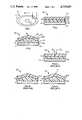
- FIG. 1illustrates generally an erasable data storage medium 10 for storing data words in which each of the data words has a plurality of bits that are a logic 1 or a logic 0.
- the erasable data storage medium 10can be an erasable optical data storage disc 12 which stores the data words over a plurality of concentric tracks T or, for example, tapes, cards or other such storage media.
- the optical disc 12also may be rotatable as in the direction shown by the arrow for data recording purposes to be described below.
- FIG. 2shows a section of a small bit area BA of the optical disc 12 for storing one data bit of logic 1 or logic 0.
- each bit area BA of the optical disc 12includes a substrate 14 and a dual layer 16 deposited on the substrate 14.
- the dual layer 16is susceptible to expansion and relaxation, to writing data thermally (expansion), to erasing data thermally and mechanically (relaxation), and to reading data optically.
- FIG. 2shows the dual layer 16 in a condition of relaxation corresponding to one logic state, e.g., logic 0, whereas FIG. 3 shows the dual layer 16 in the condition of expansion representing the other logic state, e.g., logic 1.
- the dual layer 16has a bottom layer 18 of one material 18A and top layer 20 of another material 20A. Neither the material 18A nor material 20A changes physical state upon expansion or relaxation of the dual layer 16.
- the material 18A and material 20Aare bonded together at their interface 22, so as to, for example, erase a data bit at a high data rate, as will be further described.
- the material 18Ais deposited on the substrate 14 such that at their interface 24, material 18A does not delaminate from substrate 14 upon expansion of the dual layer 16, as shown in FIG. 3. This substantially eliminates any "creep" of layer 18 about substrate 14, whereby the bit area BA will remain smooth over repeated erase/write cycles, as will be further described.
- material 18A and material 20Aupon expansion of the dual layer 16, and as a result of the bonding at interface 22 and at interface 24, material 18A and material 20A will continue to be bonded together, while material 18A will still be in contact with, or not have delaminated from, substrate 14.
- FIG. 3shows that the material 18A and the material 20A are deformed during expansion and, consequently, mechanical forces are produced in response to the expansion of the dual layer 16. As will be further described, these forces function, in part, to relax the dual layer 16 to the condition shown in FIG. 2 for purposes of quickly erasing a data bit.
- Material 18Ahas (1) low thermal conductivity, (2) a high coefficient of thermal expansion, (3) a glass transition temperature, T g , considerably below the glass transition temperature of material 20A, below which material 18A is glassy. That is, in connection with property (3), the material 18A may be rubbery at ambient temperature as opposed, for example, to being in a glassy or brittle condition. This means that only relatively low-power heating is required to heat the rubbery material, resulting in localized, extensive or large, and rapid expansion of the material 18A due to these three properties, respectively. Also as a result of this localized expansion, high data storage density can be achieved. Material 18A also may be relatively highly cross-linked, so that upon expansion there is substantially no viscuous flow of this material. In addition, material 18A is elastic, having a high yield strain, so that upon being held in an extended state, it will not exceed its elastic limit. Other properties and characteristics of material 18A will be described below.
- Material 20Ahas (1) a glass transition temperature, T g , considerably above that of material 18A, for example 100° C., which is higher than ambient temperature. Thus, at ambient or normal temperatures material 20A is glassy or brittle, but when heated above the glass transition temperature, T g , immediately transforms through a leathery or pliable condition into a rubbery condition. Material 20A also has (2) a relatively low thermal conductivity. Therefore, low-power heat can be used to quickly and locally, but only slightly, expand material 20A due to these properties.
- T gglass transition temperature
- Material 20Amay be either lightly cross-linked or depend upon chain entanglements to prevent excessive flow, and may thus be either thermoplastic or thermoset with a relatively low yield strain. Therefore, upon expansion, the cross-linking or entanglements limits the viscous flow and a stretching of material 20A occurs.
- material 20Ahas a modulus of elasticity that varies with temperature.
- the modulusdecreases with increasing temperature. This results in a reversible viscoelastic strain being induced very quickly at low light power, which holds the bump B, as shown in FIG. 3.
- Substrate 14is a material that may, but not necessarily, have a low coefficient of thermal expansion.
- Layer 18 and layer 20are optically coupled, so that substantially all the light that is propagated through layer 20 is absorbed in layer 18.
- This optical couplingis provided by the material 20A having about the same index of refraction as material 18A.
- substantially all this lightcan be coupled through top layer 20 to bottom layer 18, there is no loss of light, and therefore, lower power light sources can be used.
- Material 18A and material 20Aare also capable of being optically tuned to any of a plurality of desired or given wavelengths of light.
- material 18A and material 20Acan each constitute a light-transparent material that has added to it a dye or pigment to cause the respective material 18A and material 20A to absorb the given wavelength of light.
- material 18A and material 20Awill be tuned to absorb different wavelengths of light with material 20A being substantially, but not entirely, transparent to the wavelength of light that can be absorbed by the material 18A.
- This optical tuninghas the advantage of making the optical data storage medium 12 highly flexible in that it can be tuned to operate with a variety of different laser sources that are currently available and inexpensive or that might be available in the future.
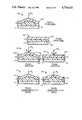
- FIG. 4A-FIG. 4Cillustrate a method for writing a data bit thermally at the bit area BA.
- the bit area BA of the erasable optical data storage medium 12is in the relaxed condition described in connection with FIG. 2.
- material 18Amay be above its glass transition temperature, T g , and, therefore, rubbery
- material 20Ais below its glass transition temperature, T g , and, therefore, glassy.
- the material 18A and material 20Ahave the other properties and characteristics previously described, including, for example, material 18A and material 20A being high yield strain and lower yield strain, respectively.
- the methodincludes heating the material 18A to expand the material 18A within its elastic limit.
- the material 20Aalso is heated above its glass transition temperature, T g , which makes the material 20A rubbery.
- T gglass transition temperature
- the heating of material 18A and material 20Ais accomplished by generating a laser beam LB 1 that has a wavelength which is substantially transparent to the material 20A and absorptive by the material 18A, and focusing the laser beam LB 1 through the material 20A onto the material 18A.
- the light of the laser beam LB 1may be slightly absorbed by the material 20A to produce the heat for making this material 20A leathery or rubbery and is substantially absorbed by material 18A for thermally expanding the material 18A onto the material 20A.
- the next stepis allowing the heated material 18A to expand and push up the heated material 20A creating a deformation or bump, while the heated material 18A expands.
- the next stepshown in FIG. 4C, includes cooling the expanded material 20A below its glass transition temperature, T g , while the material 18A is in the expanded condition. Upon cooling, the material 20A forms a reversibly fixed deformation or bump B and holds the material 18A in the expanded condition.
- a data bit of one logic levele.g., logic 1 has been written with the bit area BA being in the expanded condition described in connection with FIG. 3. If a logic 0 were to be written at the bit area BA, then laser beam LB 1 would not be actuated and the bit area BA would remain in the relaxed condition shown in FIG. 2.
- material 20Amay absorb no such light. Rather, a small amount of the heat that is absorbed in material 18A is conducted or transferred to material 20A to heat the latter above its glass transition temperature, T g .
- the methodcan include first heating the material 20A above its glass transition temperature, T g , by generating a laser beam LB 2 shown in dotted lines and focusing the laser beam LB 2 on the material 20A.
- the laser beam LB 2is of a wavelength that is substantially absorbed by material 20A.
- the laser beam LB 1is actuated and focused on the material 18A as described above, with the method for writing the data bit thermally continuing also as described above.
- One advantage to using the laser beam LB 2initially is to more quickly bring the material 20A to a rubbery condition and, thereby, be able to write a data bit more quickly.
- FIG. 5A-FIG. 5Cdisclose the method for erasing a data bit thermally and mechanically.
- the bit area BAhas a data bit written as illustrated in FIG. 5A, which shows the same expanded condition for the bit area BA as in FIG. 4C in which the material 20A is holding the material 18A in an expanded condition at ambient temperature.
- the methodincludes heating the material 20A to a temperature above the glass transition temperature, T g , to make the material 20A rubbery. This heating of the material 20A, as shown in FIG. 5A, can be accomplished by generating and focusing the laser beam LB 2 onto material 20A.
- the heating of material 20Acauses a relaxation of the holding by the material 20A of the material 18A, thereby allowing the mechanical forces previously mentioned to rapidly return the bit area BA to the relaxed condition shown in FIG. 4A.
- the elastic force in the material 18Aassists in causing a quick return of the dual layer 16 to the relaxed condition.
- the material 20A and the overall dual layer 16returns to the fully relaxed condition, as shown in FIG. 5B and as was described in connection with FIG. 2.
- the dual layer 16, upon cooling,returns to a smooth condition.
- the dual layer 16has a relaxation time which is dependent, in part, on forces produced in response to the viscoelastic properties of the material 18A.
- FIG. 6A-FIG. 6Billustrate a method of reading a data bit optically.
- a data bitfor example, a logic 1
- the laser beam LB 1which is at a lower power level than is used for writing or erasing the data bit, is generated and focused on the bump B of the material 20A.
- a data bit of logic 0has been written in the bit area BA, as shown in FIG. 6B, i.e., no bump B is produced.
- the laser beam LB 1 at lower power level than is used for writing or erasing the data bitis generated and focused on the material 20A.
- the light of laser beam LB 1will be reflected from the material 20A. Due to the difference in thickness or height H between the expanded condition of dual layer 16 shown in FIG. 6A and the relaxed condition of the dual layer 16 shown in FIG. 6B, there is a phase shift between the light of laser beam LB 1 that is reflected from the material 20A, respectively. This phase shift or difference can be detected with a high signal-to-noise ratio to distinguish a logic 1 from a logic 0 bit. Alternatively, there will be a difference in amplitude of the reflected light between the FIG. 6A and FIG. 6B conditions of bit area BA. This difference in amplitude can be detected with a high signal-to-noise ratio as logic 1 and logic 0 bits, respectively. More light scattering and, hence, reduced amplitude will be detected in the FIG. 6A condition than the FIG. 6B condition.
- FIG. 7A-FIG. 7Bare used to explain an erase/write cycle for erasing one data bit and writing another data bit at one bit area BA.
- the erase/write cycleoccurs rapidly within the same view of an objective lens used to focus laser beam LB 1 and LB 2 on the material 18A and the material 20A, respectively, as the bit area BA moves across the lens.
- the erase/write cyclethen includes first heating the material 20A at the bit area BA to erase the bit.
- the heatingcan be accomplished by generating and focusing the laser beam LB 2 on the material 20A to heat the material above its glass transition temperature, T g , to a rubbery condition.
- another data bite.g., a logic 1 is written at the bit area BA in the manner previously described for the Write Mode.
- This step of writingincludes generating and focusing the laser beam LB 1 on the material 18A, as shown in FIG.
- the material 18A and the material 20Apreferably are polymers, and particularly, amorphous polymers.
- the material 18Acan be, for example, elastomers having the above-mentioned thermoelastic properties and characteristics.
- the elastomerscan include butyl rubbers, silicone rubbers, natural rubbers, ethylene-copolymers, polyurethanes, styrene-butadiene rubbers, and a number of other synthetic elastomers.
- the amorphous polymers of the material 20Aare those having the thermosetting or thermoplastic properties with characteristics mentioned above. These may include, for example, cellulose esters, polystyrenes, polysulfones, polycarbonates, polyacrylates, poly (vinyl acetates), polyamides and a wide variety of combinations thereof. Other amorphous polymers that can also be used include, for example, acrylic polymers, silicone copolymers, epoxy resins, alkyd resins, styrene copolymers, cellulose ethers, polyvinyl alcohol, and various other polymers.
- colorantsexamples include phthalocyanines, carbon blacks, azos (monoazo and disazo), anthroquinones, azines (nigrosenes) and xanthenes.
- colorantswhich are suitable are Sudan Black 60, Solvent Red 92, Solvent Blue 44, Solvent Blue 45, Neozapon Blue 807, Macrolex Blue RR, Perox Red 32, Heliogen Blue K, Phthalo Green E and mixtures thereof.
- dyesmight include some of those listed in U.S. Pat. Nos. 3,689,768, column 3, lines 1-22 and 4,336,545, column 8, lines 53-68.
- Dow Corning 734a clear silicone rubber, having a volumetric coefficient of thermal expansion of 920 ⁇ 10 -6 cm 3 /cm 3 /°C., was mixed with a carbon black pigment manufactured by the Cabot Corporation.
- the material 18Awas then applied to the material 20A by using a "knife spread" technique. Then, the dual layer 16 was released or taken off the mandrel and mounted on a substrate 14 of aluminum.
- the fabricated substrate 14 and the dual layer 16were then mounted in a "single-shot" laser system having a Krypton laser at a wavelength of 647 nanometers. Then, to write a data bit, the laser was actuated for 50 nanoseconds using an electro-optical crystal, with the laser light then propagated through a shutter, a 25 micron pinhole and a 0.45 N.A. objective lens which was anti-reflective coated. The laser power was at 820-880 milliwatts, with about 20-30% of this power being provided at the dual layer 16. Bumps B were created in the range of 2.5-5 microns in diameter.
- a "single-shot" erase systemhaving an Argon laser at a wavelength of 488 nanometers was used.
- the laser beamwas modulated using an electro-optical modulator and was focused on bumps B through a microscope system using a 20 ⁇ objective lens.
- the laserwas operated at 1 microsecond pulse duration times and at 55 milliwatts of power, with about 11-12% of this power being applied at the dual layer 16.
- the bumps Bwere erased, as previously described.
- the data bits that were written on the fabricated substrate 14 and the dual layer 16were read using white light and a microscope to project images of the bumps B on a glass plate. Then, using a fiber optic bundle hooked to a photomultiplier, the intensity of the light at the glass plate was detected. It was found that a satisfactory contrast ratio of about 2:1 to 3:1 existed between areas of the glass plate having the bumps B and areas of the glass plate having no bumps B.
- FIG. 8illustrates one embodiment of a practical electro-optical system 26 for carrying out the optical recording of data on the erasable optical data storage medium 12.
- FIG. 8shows one bit area BA, similar to the bit area BA shown in FIG. 2, for writing, reading and erasing a bit as described above.
- Electro-optical system 26includes a digital data processing circuit 28 whose outputs on respective lines 30 and 32 control respective pulsed variable-intensity lasers 34 and 36.
- Laser 34outputs the laser beam LB 2 and laser 36 outputs the laser beam LB 1 .
- a pair of lenses 38 and 40collimate the laser beams LB 2 and LB 1 , respectively, which are then reflected by a mirror 42 and propagated through a beam splitter 44.
- the laser beam LB 2 and laser beam LB 1are then passed through a filter 46 (e.g. 1/4 waveplate) and then propagated through an objective lens 48 which focuses the laser beams on the moving bit area BA.
- a filter 46e.g. 1/4 waveplate
- an objective lens 48which focuses the laser beams on the moving bit area BA.
- Light reflected by the material 20A of bit area BAis collected by the lens 48 and propagated through filter 46 to the beam splitter 44, where the reflected light is then propagated to a light sensor 50.
- laser beam LB 2 and laser beam LB 1are spatially separated from one another. Also, the laser beam LB 2 is focused onto the bit area BA ahead of the laser beam LB 1 relative to the direction of movement of the bit area BA for erase/write purposes to be described below.
- the laser 34is modulated by the output of the data processing circuit 28 on line 30 to produce a high intensity laser beam LB 2 .
- the laser beam LB 2is then focused on the material 20A by lens 48 to heat it to a rubbery condition.
- the laser 36is immediately modulated by the output of data processing circuit 28 over line 32 to produce the laser beam LB 1 . Consequently, the laser beam LB 1 is focused by the objective lens 48 onto the material 18A to heat it and cause the elastic expansion previously described.
- bit area BAwill move out of the view of the objective lens 48 and cool, so that either a logic 1 or a logic 0 will be written.
- the erase/write cyclecan occur within one bit cell time, which means within the same view of the objective lens 48.
- the data processing circuit 28, via line 30,modulates the laser 34 to output a high intensity laser beam LB 2 which is then focused on the material 20A. Therefore, the material 20A is heated and then cools as the bit area moves outside the view of the objective lens 48. The result is that the bit will be erased in the manner previously described.
- bit area BAwhich bit is either a logic 1 or a logic 0.
- the data processing circuit 28modulates laser 34 to produce a low intensity laser beam LB 1 that is focused on the material 20A.
- the reflected lightis then collected by lens 48 and propagated by filter 48 and beam splitter 44 to sensor 50 which then detects the logic state of the bit.
- differences in phase or amplitude of the reflected lightcan be detected by sensor 50 to distinguish a logic 1 from a logic 0.
- FIG. 9is similar to FIG. 8 except that rather than having spatially separated laser beams LB 1 and LB 2 , the two laser beams are concentric or co-linear.
- the co-linear beams LB 1 and LB 2are propagated so that they are focused co-linearly on the material 18A and the material 20A as the bit area BA moves within the view of the objective lens 48.
- the co-linear laser beams LB 1 and LB 2are produced by having laser 34 and laser 36 arranged, as shown, whereby light from each laser is propagated through a beam splitter BS.
- the erase/write cycle, the erase cycle and the read cycle in FIG. 9are performed in a manner similar to that described for FIG. 8.
Landscapes
- Optical Recording Or Reproduction (AREA)
Abstract
Description
Claims (21)
Priority Applications (2)
| Application Number | Priority Date | Filing Date | Title |
|---|---|---|---|
| US06/835,960US4719615A (en) | 1983-08-22 | 1986-03-04 | Erasable optical data storage medium |
| US06/848,725US4852075A (en) | 1983-08-22 | 1986-04-04 | Erasable optical data storage medium and method and apparatus for recording data on the medium |
Applications Claiming Priority (2)
| Application Number | Priority Date | Filing Date | Title |
|---|---|---|---|
| US52581383A | 1983-08-22 | 1983-08-22 | |
| US06/835,960US4719615A (en) | 1983-08-22 | 1986-03-04 | Erasable optical data storage medium |
Related Parent Applications (1)
| Application Number | Title | Priority Date | Filing Date |
|---|---|---|---|
| US52581383AContinuation-In-Part | 1983-08-22 | 1983-08-22 |
Related Child Applications (1)
| Application Number | Title | Priority Date | Filing Date |
|---|---|---|---|
| US06/848,725DivisionUS4852075A (en) | 1983-08-22 | 1986-04-04 | Erasable optical data storage medium and method and apparatus for recording data on the medium |
Publications (1)
| Publication Number | Publication Date |
|---|---|
| US4719615Atrue US4719615A (en) | 1988-01-12 |
Family
ID=27061909
Family Applications (1)
| Application Number | Title | Priority Date | Filing Date |
|---|---|---|---|
| US06/835,960Expired - LifetimeUS4719615A (en) | 1983-08-22 | 1986-03-04 | Erasable optical data storage medium |
Country Status (1)
| Country | Link |
|---|---|
| US (1) | US4719615A (en) |
Cited By (97)
| Publication number | Priority date | Publication date | Assignee | Title |
|---|---|---|---|---|
| US4780867A (en)* | 1986-10-02 | 1988-10-25 | Optical Data, Inc. | Method for erasably recording data by viscoelastic shear deformation |
| US4825430A (en)* | 1986-12-19 | 1989-04-25 | Optical Data, Inc. | Erasable optical data storage medium having an embedded servo track and a subsurface recording interface |
| US4852077A (en)* | 1988-02-05 | 1989-07-25 | Tandy Corporation | Optical data storage media with spatially variable energy absorptivity |
| US4855992A (en)* | 1987-02-13 | 1989-08-08 | Kabushiki Kaisha Toshiba | Reversible optical recording medium with an optothermally deformable recording layer |
| WO1989007311A1 (en)* | 1988-02-05 | 1989-08-10 | Tandy Corporation | Optical media reflective materials |
| WO1989007312A1 (en)* | 1988-02-05 | 1989-08-10 | Tandy Corporation | Recording method and apparatus |
| US4862447A (en)* | 1985-12-11 | 1989-08-29 | U.S. Philips Corporation | Optical record carrier with surface layer extending to the center of a substantially circular information track structure therein |
| US4875204A (en)* | 1986-02-07 | 1989-10-17 | Institut Problem Modelirovania V Energetike Akademii Nauk Ukrainskoi Ssr | Method of erasing information |
| US4879709A (en)* | 1988-02-05 | 1989-11-07 | Tandy Corporation | Dye-polymer optical data storage media with improved recording sensitivity |
| US4896314A (en)* | 1988-04-19 | 1990-01-23 | Optical Data, Inc. | Bump-forming media including thin intermediate reflective layer and methods for writing, reading, and erasing same |
| US4901304A (en)* | 1986-10-08 | 1990-02-13 | Optical Data, Inc. | Erasable optical data storage medium having a zoned integral recording layer |
| US4908814A (en)* | 1986-02-07 | 1990-03-13 | Institut Problem Modelirovanija V Energetiki An Ukr. Ssr | Method of photothermal information recording reading and erasing |
| US4970711A (en)* | 1988-02-05 | 1990-11-13 | Tandy Corporation | Bulk eraser for optical memory media |
| WO1990014663A1 (en)* | 1989-05-25 | 1990-11-29 | Tandy Corporation | Interactive optical disk, method of fabrication and apparatus for recording thereon |
| WO1990014657A1 (en)* | 1989-05-25 | 1990-11-29 | Tandy Corporation | Recording media |
| WO1990014664A1 (en)* | 1989-05-25 | 1990-11-29 | Tandy Corporation | Interactive optical disk, and systems and methods for using |
| US5001699A (en)* | 1988-02-05 | 1991-03-19 | Tandy Corporation | Recording method and apparatus |
| WO1991005344A1 (en)* | 1989-09-28 | 1991-04-18 | Tandy Corporation | Single polymer layer recordable/erasable optical media |
| US5009986A (en)* | 1989-01-17 | 1991-04-23 | Teijin Limited | Naphthalocyanine based compound and optical recording medium containing the same |
| US5014259A (en)* | 1988-02-05 | 1991-05-07 | Tandy Corporation | Recording medium having an insulating layer |
| US5016239A (en)* | 1988-02-05 | 1991-05-14 | Tandy Corporation | Recording method and apparatus |
| US5018128A (en)* | 1988-02-05 | 1991-05-21 | Tandy Corporation | Apparatus and medium for recording erasable information |
| US5019487A (en)* | 1988-02-11 | 1991-05-28 | U.S. Philips Corporation | Method of manufacturing a metal matrix and a master disc suitable for the manufacture of matrices |
| US5036511A (en)* | 1988-02-05 | 1991-07-30 | Tandy Corporation | Recording method and apparatus |
| US5043971A (en)* | 1989-09-28 | 1991-08-27 | Tandy Corporation | Method and apparatus for pre-compensation in an optical disc |
| US5056081A (en)* | 1990-01-02 | 1991-10-08 | Tandy Corporation | System and method for erasing light-responsive optical disks |
| US5088087A (en)* | 1990-07-25 | 1992-02-11 | Tandy Corporation | Dual-metal reflective layer recordable/erasable optical media |
| US5088088A (en)* | 1988-02-05 | 1992-02-11 | Tandy Corporation | Dye-polymer optical data storage media with improved recording sensitivity |
| US5090008A (en)* | 1988-02-05 | 1992-02-18 | Tandy Corporation | Erasable recording media |
| US5106721A (en)* | 1988-01-06 | 1992-04-21 | U.S. Phillips Corporation | Method of recording information, recording element manufactured according to the method and method of producing a metal matrix |
| US5128921A (en)* | 1989-09-28 | 1992-07-07 | Tandy Corporation | Method and apparatus for pre-compensation in an optical disc |
| US5143854A (en)* | 1989-06-07 | 1992-09-01 | Affymax Technologies N.V. | Large scale photolithographic solid phase synthesis of polypeptides and receptor binding screening thereof |
| US5144613A (en)* | 1990-07-26 | 1992-09-01 | Tandy Corporation | Thermal bulk erasure method for dye polymer optical media |
| US5153873A (en)* | 1988-05-24 | 1992-10-06 | U.S. Philips Corporation | Optical record carrier and method and apparatus for increasing the resolution of information recorded thereon and read therefrom |
| US5186995A (en)* | 1989-07-06 | 1993-02-16 | Pioneer Electronic Corporation | Optical disk |
| US5208801A (en)* | 1988-02-05 | 1993-05-04 | Tandy Corporation | Method and apparatus for correcting focus in an optical recording system |
| US5214632A (en)* | 1987-12-23 | 1993-05-25 | U.S. Philips Corporation | Method of manufacturing a matrix and a master plate suitable for use in the method |
| US5216658A (en)* | 1990-07-26 | 1993-06-01 | Tandy Corporation | Enlarged-spot erasure of optical media in dual-beam systems |
| US5215800A (en)* | 1989-01-17 | 1993-06-01 | Teijin Limited | Erasable optical recording medium and method for writing, reading and/or erasing thereof |
| US5231624A (en)* | 1991-08-01 | 1993-07-27 | Tandy Corporation | System and method using a reduce profile light beam for high density recording on optical media |
| US5241165A (en)* | 1981-02-27 | 1993-08-31 | Drexler Technology Corporation | Erasable optical wallet-size data card |
| US5252743A (en)* | 1989-11-13 | 1993-10-12 | Affymax Technologies N.V. | Spatially-addressable immobilization of anti-ligands on surfaces |
| US5319622A (en)* | 1990-02-09 | 1994-06-07 | Ast Research, Inc. | Control and information disk for disk recording system |
| US5321684A (en)* | 1992-09-15 | 1994-06-14 | Sri International | Bidirectional sinusoidal scanning system |
| US5330799A (en)* | 1992-09-15 | 1994-07-19 | The Phscologram Venture, Inc. | Press polymerization of lenticular images |
| US5343458A (en)* | 1992-09-15 | 1994-08-30 | Samsung Electronics Co., Ltd. | Method of storing digital video, audio and control information on an an optical storage medium |
| US5363200A (en)* | 1992-09-15 | 1994-11-08 | Samsung Electronics Co., Ltd. | Buffering method and system for resonant scanner used to read and write data with respect to a storage medium |
| US5392272A (en)* | 1993-03-29 | 1995-02-21 | Sri International | Single erasable optical recording layer having both retention and expansion characteristics |
| US5428599A (en)* | 1992-06-18 | 1995-06-27 | Canon Kabushiki Kaisha | Optical recording medium, information recording method and information reproducing method |
| USRE35029E (en)* | 1989-01-13 | 1995-08-29 | The Phscologram Venture, Inc. | Computer-generated autostereography method and apparatus |
| US5467327A (en)* | 1993-12-22 | 1995-11-14 | Jamail; Randall | Method of masking data on a storage medium |
| US5471443A (en)* | 1993-12-22 | 1995-11-28 | Randall Jamail | Method of selectively concealing magneto-optical compact disk data for playback upon demand |
| US5508087A (en)* | 1992-05-30 | 1996-04-16 | Cheil Synthetics Inc. | Organic-optic recording tapes |
| US5519794A (en)* | 1994-04-01 | 1996-05-21 | Rotaventure L.L.C. | Computer-generated autostereography method and apparatus |
| US5604838A (en)* | 1992-09-15 | 1997-02-18 | Samsung Electronics Co., Ltd. | Method and apparatus for recording and reading a multiplexed video signal |
| US5684776A (en)* | 1994-08-25 | 1997-11-04 | Discovision Associates | Cartridge-loading apparatus with improved parking arm |
| US5808974A (en)* | 1993-12-22 | 1998-09-15 | Jamail; Randall H. | Method of masking data on a storage medium using a directory |
| US5995457A (en)* | 1993-12-22 | 1999-11-30 | Jamail; Randall H. | Method of masking data on digital video disks (DVD) |
| US6009061A (en)* | 1994-08-25 | 1999-12-28 | Discovision Associates | Cartridge-loading apparatus with improved base plate and cartridge receiver latch |
| US6309822B1 (en) | 1989-06-07 | 2001-10-30 | Affymetrix, Inc. | Method for comparing copy number of nucleic acid sequences |
| US6310189B1 (en) | 1989-06-07 | 2001-10-30 | Affymetrix, Inc. | Nucleotides and analogs having photoremoveable protecting groups |
| US6355432B1 (en) | 1989-06-07 | 2002-03-12 | Affymetrix Lnc. | Products for detecting nucleic acids |
| US6379895B1 (en) | 1989-06-07 | 2002-04-30 | Affymetrix, Inc. | Photolithographic and other means for manufacturing arrays |
| US6391937B1 (en) | 1998-11-25 | 2002-05-21 | Motorola, Inc. | Polyacrylamide hydrogels and hydrogel arrays made from polyacrylamide reactive prepolymers |
| US6406844B1 (en) | 1989-06-07 | 2002-06-18 | Affymetrix, Inc. | Very large scale immobilized polymer synthesis |
| US6420169B1 (en) | 1989-06-07 | 2002-07-16 | Affymetrix, Inc. | Apparatus for forming polynucleotides or polypeptides |
| US6451536B1 (en) | 1990-12-06 | 2002-09-17 | Affymetrix Inc. | Products for detecting nucleic acids |
| US20020137096A1 (en)* | 1989-06-07 | 2002-09-26 | Affymetrix, Inc. | Apparatus comprising polymers |
| US6468740B1 (en) | 1992-11-05 | 2002-10-22 | Affymetrix, Inc. | Cyclic and substituted immobilized molecular synthesis |
| US6475588B1 (en) | 2001-08-07 | 2002-11-05 | General Electric Company | Colored digital versatile disks |
| US6475589B1 (en) | 2001-12-17 | 2002-11-05 | General Electric Company | Colored optical discs and methods for making the same |
| US20030008302A1 (en)* | 1990-12-06 | 2003-01-09 | Affymax Technologies, N.V. | Sequencing of surface immobilized polymers utilizing microfluorescence detection |
| US6506558B1 (en) | 1990-03-07 | 2003-01-14 | Affymetrix Inc. | Very large scale immobilized polymer synthesis |
| US6545264B1 (en) | 1998-10-30 | 2003-04-08 | Affymetrix, Inc. | Systems and methods for high performance scanning |
| US6551784B2 (en) | 1989-06-07 | 2003-04-22 | Affymetrix Inc | Method of comparing nucleic acid sequences |
| US6566495B1 (en) | 1989-06-07 | 2003-05-20 | Affymetrix, Inc. | Very large scale immobilized polymer synthesis |
| US6570840B1 (en) | 2000-04-26 | 2003-05-27 | Optical Disc Corporation | Figure of merit in optical recording structures |
| US20030138363A1 (en)* | 1998-02-11 | 2003-07-24 | The Regents Of The University Of Michigan | Device for chemical and biochemical reactions using photo-generated reagents |
| US20030152774A1 (en)* | 2000-09-29 | 2003-08-14 | Curtis Cradic | Colored data storage media |
| US20030161254A1 (en)* | 2002-02-26 | 2003-08-28 | Blankenbeckler David L. | Dual density disc with associated properties |
| US6628598B2 (en) | 2000-12-05 | 2003-09-30 | Imation Corp. | Patterned media system |
| US20030235120A1 (en)* | 2001-07-23 | 2003-12-25 | Hiroshi Nakayama | Optical recording medium preheat bulk erase apparatus, optical recording medium preheat bulk erase method, and optical recording medium |
| US20040035690A1 (en)* | 1998-02-11 | 2004-02-26 | The Regents Of The University Of Michigan | Method and apparatus for chemical and biochemical reactions using photo-generated reagents |
| US6751060B2 (en) | 2000-12-05 | 2004-06-15 | Imation Corp. | Magnetic media with readable topographical features |
| US20050118706A1 (en)* | 1989-06-07 | 2005-06-02 | Affymetrix, Inc. | Polymer arrays |
| US20050185175A1 (en)* | 2002-07-16 | 2005-08-25 | Canos Avelino C. | Rotary support and apparatus used for the multiple spectroscopic characterisation of samples of solid materials |
| US7094609B2 (en) | 1996-09-20 | 2006-08-22 | Burstein Technologies, Inc. | Spatially addressable combinatorial chemical arrays in encoded optical disk format |
| US20080227653A1 (en)* | 1989-06-07 | 2008-09-18 | Fodor Stephen P A | Expression monitoring by hybridization to high density oligonucleotide arrays |
| EP2573101A1 (en) | 1996-02-09 | 2013-03-27 | Cornell Research Foundation, Inc. | Detection of nucleic acid sequence differences using the ligase detection reaction with addressable arrays |
| US8953427B2 (en) | 2010-10-19 | 2015-02-10 | Fujifilm Corporation | Optical information recording medium |
| US9368144B2 (en) | 2012-09-27 | 2016-06-14 | Fujifilm Corporation | Optical information recording medium and method for manufacturing same |
| US9406332B2 (en) | 2013-03-08 | 2016-08-02 | Fujifilm Corporation | Optical information recording medium |
| US20170251625A1 (en)* | 2014-09-16 | 2017-09-07 | BMA Automation GmbH | Method and device for removing a plastic coating from a block of food |
| WO2019186569A1 (en) | 2018-03-29 | 2019-10-03 | Yeda Research And Development Co. Ltd. | Use of electric field gradients to control gene expression |
| WO2021059269A1 (en) | 2019-09-25 | 2021-04-01 | Yeda Research And Development Co. Ltd. | Assembly of protein complexes on a chip |
| WO2023238132A1 (en) | 2022-06-07 | 2023-12-14 | Yeda Research And Development Co. Ltd. | Microfluidic device for analyzing steady state biological reactions |
| WO2025104733A1 (en) | 2023-11-14 | 2025-05-22 | Yeda Research And Development Co. Ltd. | Chips for determining binding affinities of biomolecules |
Citations (23)
| Publication number | Priority date | Publication date | Assignee | Title |
|---|---|---|---|---|
| US3689768A (en)* | 1970-06-18 | 1972-09-05 | Masamichi Sato | Electron beam recording materials |
| US3787873A (en)* | 1970-10-12 | 1974-01-22 | Fuji Photo Film Co Ltd | Laser recording method and material therefor |
| US4264986A (en)* | 1979-03-12 | 1981-04-28 | Willis Craig I | Information-recording process & apparatus |
| US4268575A (en)* | 1978-08-07 | 1981-05-19 | Fuji Photo Film Co., Ltd. | Thermal recording elements |
| US4278734A (en)* | 1978-08-17 | 1981-07-14 | Matsushita Electric Industrial Co., Ltd. | Optical information recording material and method of recording and reproducing information using same material |
| US4282534A (en)* | 1978-06-26 | 1981-08-04 | Fuji Photo Film Co., Ltd. | Thermal recording elements |
| US4285056A (en)* | 1979-10-17 | 1981-08-18 | Rca Corporation | Replicable optical recording medium |
| US4320489A (en)* | 1980-03-03 | 1982-03-16 | Rca Corporation | Reversible optical storage medium and a method for recording information therein |
| JPS5760546A (en)* | 1980-09-30 | 1982-04-12 | Fujitsu Ltd | Optical recording medium |
| US4336545A (en)* | 1980-12-18 | 1982-06-22 | Eastman Kodak Company | Optical disc structure, method and apparatus physically optimized for writing and reading with a single wavelength |
| US4360895A (en)* | 1980-02-01 | 1982-11-23 | Thomson-Csf | Permanent memory structure with thermo-optical writing and optical reading and writing process in such a structure |
| US4371954A (en)* | 1980-02-01 | 1983-02-01 | Thomson-Csf | Reversible memory structure with thermo-optical writing and optical reading and process for writing and erasing said structure |
| JPS5862096A (en)* | 1981-10-09 | 1983-04-13 | Matsushita Electric Ind Co Ltd | optical information recording carrier |
| JPS5894145A (en)* | 1981-11-30 | 1983-06-04 | Tdk Corp | Optical recording tape |
| US4398203A (en)* | 1980-08-13 | 1983-08-09 | Thomson-Csf | Thermo-optical method for writing information and an information medium for the application of said method |
| US4404656A (en)* | 1980-01-23 | 1983-09-13 | Thomson-Csf | Thermo-optical data writing process and data medium for performing this process |
| US4405994A (en)* | 1980-01-23 | 1983-09-20 | Thomson-Csf | Thermo-optic information writing process and information support for implementing this process |
| US4430659A (en)* | 1981-02-13 | 1984-02-07 | Minnesota Mining And Manufacturing Company | Protuberant optical recording medium |
| US4463083A (en)* | 1978-06-29 | 1984-07-31 | Fuji Photo Film Co., Ltd. | Thermal recording elements |
| US4478782A (en)* | 1982-06-21 | 1984-10-23 | Celanese Corporation | Erasable recording medium comprising a dimer acid polyamide resin |
| US4554655A (en)* | 1982-02-24 | 1985-11-19 | Pioneer Video Corporation | Optical data recording disc and system |
| US4578788A (en)* | 1983-06-02 | 1986-03-25 | International Business Machines Corporation | High performance optical storage medium with separate mechanical servo tracks embedded within the medium |
| US4647947A (en)* | 1982-03-15 | 1987-03-03 | Tokyo Shibaura Denki Kabushiki Kaisha | Optical protuberant bubble recording medium |
- 1986
- 1986-03-04USUS06/835,960patent/US4719615A/ennot_activeExpired - Lifetime
Patent Citations (23)
| Publication number | Priority date | Publication date | Assignee | Title |
|---|---|---|---|---|
| US3689768A (en)* | 1970-06-18 | 1972-09-05 | Masamichi Sato | Electron beam recording materials |
| US3787873A (en)* | 1970-10-12 | 1974-01-22 | Fuji Photo Film Co Ltd | Laser recording method and material therefor |
| US4282534A (en)* | 1978-06-26 | 1981-08-04 | Fuji Photo Film Co., Ltd. | Thermal recording elements |
| US4463083A (en)* | 1978-06-29 | 1984-07-31 | Fuji Photo Film Co., Ltd. | Thermal recording elements |
| US4268575A (en)* | 1978-08-07 | 1981-05-19 | Fuji Photo Film Co., Ltd. | Thermal recording elements |
| US4278734A (en)* | 1978-08-17 | 1981-07-14 | Matsushita Electric Industrial Co., Ltd. | Optical information recording material and method of recording and reproducing information using same material |
| US4264986A (en)* | 1979-03-12 | 1981-04-28 | Willis Craig I | Information-recording process & apparatus |
| US4285056A (en)* | 1979-10-17 | 1981-08-18 | Rca Corporation | Replicable optical recording medium |
| US4404656A (en)* | 1980-01-23 | 1983-09-13 | Thomson-Csf | Thermo-optical data writing process and data medium for performing this process |
| US4405994A (en)* | 1980-01-23 | 1983-09-20 | Thomson-Csf | Thermo-optic information writing process and information support for implementing this process |
| US4360895A (en)* | 1980-02-01 | 1982-11-23 | Thomson-Csf | Permanent memory structure with thermo-optical writing and optical reading and writing process in such a structure |
| US4371954A (en)* | 1980-02-01 | 1983-02-01 | Thomson-Csf | Reversible memory structure with thermo-optical writing and optical reading and process for writing and erasing said structure |
| US4320489A (en)* | 1980-03-03 | 1982-03-16 | Rca Corporation | Reversible optical storage medium and a method for recording information therein |
| US4398203A (en)* | 1980-08-13 | 1983-08-09 | Thomson-Csf | Thermo-optical method for writing information and an information medium for the application of said method |
| JPS5760546A (en)* | 1980-09-30 | 1982-04-12 | Fujitsu Ltd | Optical recording medium |
| US4336545A (en)* | 1980-12-18 | 1982-06-22 | Eastman Kodak Company | Optical disc structure, method and apparatus physically optimized for writing and reading with a single wavelength |
| US4430659A (en)* | 1981-02-13 | 1984-02-07 | Minnesota Mining And Manufacturing Company | Protuberant optical recording medium |
| JPS5862096A (en)* | 1981-10-09 | 1983-04-13 | Matsushita Electric Ind Co Ltd | optical information recording carrier |
| JPS5894145A (en)* | 1981-11-30 | 1983-06-04 | Tdk Corp | Optical recording tape |
| US4554655A (en)* | 1982-02-24 | 1985-11-19 | Pioneer Video Corporation | Optical data recording disc and system |
| US4647947A (en)* | 1982-03-15 | 1987-03-03 | Tokyo Shibaura Denki Kabushiki Kaisha | Optical protuberant bubble recording medium |
| US4478782A (en)* | 1982-06-21 | 1984-10-23 | Celanese Corporation | Erasable recording medium comprising a dimer acid polyamide resin |
| US4578788A (en)* | 1983-06-02 | 1986-03-25 | International Business Machines Corporation | High performance optical storage medium with separate mechanical servo tracks embedded within the medium |
Non-Patent Citations (2)
| Title |
|---|
| Elements of Materials Science, 2nd. Ed., by Von Vlack, Addison Wesley Publishing Co., 1967, pp. 76, 77.* |
| Elements of Materials Science, 2nd. Ed., by Von Vlack, Addison-Wesley Publishing Co., ©1967, pp. 76, 77. |
Cited By (177)
| Publication number | Priority date | Publication date | Assignee | Title |
|---|---|---|---|---|
| US5241165A (en)* | 1981-02-27 | 1993-08-31 | Drexler Technology Corporation | Erasable optical wallet-size data card |
| US4862447A (en)* | 1985-12-11 | 1989-08-29 | U.S. Philips Corporation | Optical record carrier with surface layer extending to the center of a substantially circular information track structure therein |
| US4875204A (en)* | 1986-02-07 | 1989-10-17 | Institut Problem Modelirovania V Energetike Akademii Nauk Ukrainskoi Ssr | Method of erasing information |
| US4908814A (en)* | 1986-02-07 | 1990-03-13 | Institut Problem Modelirovanija V Energetiki An Ukr. Ssr | Method of photothermal information recording reading and erasing |
| US4780867A (en)* | 1986-10-02 | 1988-10-25 | Optical Data, Inc. | Method for erasably recording data by viscoelastic shear deformation |
| US4901304A (en)* | 1986-10-08 | 1990-02-13 | Optical Data, Inc. | Erasable optical data storage medium having a zoned integral recording layer |
| US4825430A (en)* | 1986-12-19 | 1989-04-25 | Optical Data, Inc. | Erasable optical data storage medium having an embedded servo track and a subsurface recording interface |
| US4855992A (en)* | 1987-02-13 | 1989-08-08 | Kabushiki Kaisha Toshiba | Reversible optical recording medium with an optothermally deformable recording layer |
| US5214632A (en)* | 1987-12-23 | 1993-05-25 | U.S. Philips Corporation | Method of manufacturing a matrix and a master plate suitable for use in the method |
| US5106721A (en)* | 1988-01-06 | 1992-04-21 | U.S. Phillips Corporation | Method of recording information, recording element manufactured according to the method and method of producing a metal matrix |
| US4879709A (en)* | 1988-02-05 | 1989-11-07 | Tandy Corporation | Dye-polymer optical data storage media with improved recording sensitivity |
| WO1989007310A1 (en)* | 1988-02-05 | 1989-08-10 | Tandy Corporation | Optical data storage media with spatially variable energy absorptivity |
| US5200948A (en)* | 1988-02-05 | 1993-04-06 | Tandy Corporation | Recording method and apparatus |
| US4918682A (en)* | 1988-02-05 | 1990-04-17 | Tandy Corporation | Ablative and bump-forming optical recording media including a metallic reflective layer |
| US5208801A (en)* | 1988-02-05 | 1993-05-04 | Tandy Corporation | Method and apparatus for correcting focus in an optical recording system |
| US4970711A (en)* | 1988-02-05 | 1990-11-13 | Tandy Corporation | Bulk eraser for optical memory media |
| US4852077A (en)* | 1988-02-05 | 1989-07-25 | Tandy Corporation | Optical data storage media with spatially variable energy absorptivity |
| US5090008A (en)* | 1988-02-05 | 1992-02-18 | Tandy Corporation | Erasable recording media |
| US5088088A (en)* | 1988-02-05 | 1992-02-11 | Tandy Corporation | Dye-polymer optical data storage media with improved recording sensitivity |
| US5001699A (en)* | 1988-02-05 | 1991-03-19 | Tandy Corporation | Recording method and apparatus |
| WO1989007311A1 (en)* | 1988-02-05 | 1989-08-10 | Tandy Corporation | Optical media reflective materials |
| WO1989007312A1 (en)* | 1988-02-05 | 1989-08-10 | Tandy Corporation | Recording method and apparatus |
| US5014259A (en)* | 1988-02-05 | 1991-05-07 | Tandy Corporation | Recording medium having an insulating layer |
| US5016239A (en)* | 1988-02-05 | 1991-05-14 | Tandy Corporation | Recording method and apparatus |
| US5018128A (en)* | 1988-02-05 | 1991-05-21 | Tandy Corporation | Apparatus and medium for recording erasable information |
| US5036511A (en)* | 1988-02-05 | 1991-07-30 | Tandy Corporation | Recording method and apparatus |
| US5019487A (en)* | 1988-02-11 | 1991-05-28 | U.S. Philips Corporation | Method of manufacturing a metal matrix and a master disc suitable for the manufacture of matrices |
| US4896314A (en)* | 1988-04-19 | 1990-01-23 | Optical Data, Inc. | Bump-forming media including thin intermediate reflective layer and methods for writing, reading, and erasing same |
| EP0338776A3 (en)* | 1988-04-19 | 1990-07-25 | Optical Data, Inc. | Bump-forming media including thin intermediate reflective layer and methods for writing, reading, and erasing same |
| US5153873A (en)* | 1988-05-24 | 1992-10-06 | U.S. Philips Corporation | Optical record carrier and method and apparatus for increasing the resolution of information recorded thereon and read therefrom |
| USRE35029E (en)* | 1989-01-13 | 1995-08-29 | The Phscologram Venture, Inc. | Computer-generated autostereography method and apparatus |
| US5009986A (en)* | 1989-01-17 | 1991-04-23 | Teijin Limited | Naphthalocyanine based compound and optical recording medium containing the same |
| US5215800A (en)* | 1989-01-17 | 1993-06-01 | Teijin Limited | Erasable optical recording medium and method for writing, reading and/or erasing thereof |
| WO1990014664A1 (en)* | 1989-05-25 | 1990-11-29 | Tandy Corporation | Interactive optical disk, and systems and methods for using |
| WO1990014657A1 (en)* | 1989-05-25 | 1990-11-29 | Tandy Corporation | Recording media |
| WO1990014663A1 (en)* | 1989-05-25 | 1990-11-29 | Tandy Corporation | Interactive optical disk, method of fabrication and apparatus for recording thereon |
| US5175720A (en)* | 1989-05-25 | 1992-12-29 | Tandy Corporation | Interactive optical disk |
| US7087732B2 (en) | 1989-06-07 | 2006-08-08 | Affymetrix, Inc. | Nucleotides and analogs having photoremovable protecting groups |
| US6660234B2 (en) | 1989-06-07 | 2003-12-09 | Affymetrix, Inc. | Apparatus for polymer synthesis |
| US20020137096A1 (en)* | 1989-06-07 | 2002-09-26 | Affymetrix, Inc. | Apparatus comprising polymers |
| US5143854A (en)* | 1989-06-07 | 1992-09-01 | Affymax Technologies N.V. | Large scale photolithographic solid phase synthesis of polypeptides and receptor binding screening thereof |
| US6440667B1 (en) | 1989-06-07 | 2002-08-27 | Affymetrix Inc. | Analysis of target molecules using an encoding system |
| US6551784B2 (en) | 1989-06-07 | 2003-04-22 | Affymetrix Inc | Method of comparing nucleic acid sequences |
| US6420169B1 (en) | 1989-06-07 | 2002-07-16 | Affymetrix, Inc. | Apparatus for forming polynucleotides or polypeptides |
| US6416952B1 (en) | 1989-06-07 | 2002-07-09 | Affymetrix, Inc. | Photolithographic and other means for manufacturing arrays |
| US6491871B1 (en) | 1989-06-07 | 2002-12-10 | Affymetrix, Inc. | System for determining receptor-ligand binding affinity |
| US6566495B1 (en) | 1989-06-07 | 2003-05-20 | Affymetrix, Inc. | Very large scale immobilized polymer synthesis |
| US6406844B1 (en) | 1989-06-07 | 2002-06-18 | Affymetrix, Inc. | Very large scale immobilized polymer synthesis |
| US6403957B1 (en) | 1989-06-07 | 2002-06-11 | Affymetrix, Inc. | Nucleic acid reading and analysis system |
| US6955915B2 (en) | 1989-06-07 | 2005-10-18 | Affymetrix, Inc. | Apparatus comprising polymers |
| US20050214828A1 (en)* | 1989-06-07 | 2005-09-29 | Affymetrix, Inc. | Very large scale immobilized polymer synthesis |
| US20050208537A1 (en)* | 1989-06-07 | 2005-09-22 | Affymetrix, Inc. | Very large scale immobilized polymer synthesis |
| US6919211B1 (en) | 1989-06-07 | 2005-07-19 | Affymetrix, Inc. | Polypeptide arrays |
| US20050153362A1 (en)* | 1989-06-07 | 2005-07-14 | Pirrung Michael C. | Polymer arrays |
| US20050153363A1 (en)* | 1989-06-07 | 2005-07-14 | Pirrung Michael C. | Polymer arrays |
| US6403320B1 (en) | 1989-06-07 | 2002-06-11 | Affymetrix, Inc. | Support bound probes and methods of analysis using the same |
| US6395491B1 (en) | 1989-06-07 | 2002-05-28 | Affymetrix, Inc. | Method of information storage and recovery |
| US20050148027A1 (en)* | 1989-06-07 | 2005-07-07 | Affymetrix Inc. | Very large scale immobilized polymer synthesis |
| US20050118706A1 (en)* | 1989-06-07 | 2005-06-02 | Affymetrix, Inc. | Polymer arrays |
| US6576424B2 (en) | 1989-06-07 | 2003-06-10 | Affymetrix Inc. | Arrays and methods for detecting nucleic acids |
| US20050079529A1 (en)* | 1989-06-07 | 2005-04-14 | Affymetrix, Inc. | Very large scale immobilized polymer synthesis |
| US6747143B2 (en) | 1989-06-07 | 2004-06-08 | Affymetrix, Inc. | Methods for polymer synthesis |
| US20040038268A1 (en)* | 1989-06-07 | 2004-02-26 | Affymetrix, Inc. | Support bound probes and methods of analysis using the same |
| US20030235853A1 (en)* | 1989-06-07 | 2003-12-25 | Affymetrix, Inc. | Very large scale immobilized polymer synthesis |
| US20080227653A1 (en)* | 1989-06-07 | 2008-09-18 | Fodor Stephen P A | Expression monitoring by hybridization to high density oligonucleotide arrays |
| US6646243B2 (en) | 1989-06-07 | 2003-11-11 | Affymetrix, Inc. | Nucleic acid reading and analysis system |
| US6630308B2 (en) | 1989-06-07 | 2003-10-07 | Affymetrix, Inc. | Methods of synthesizing a plurality of different polymers on a surface of a substrate |
| US6610482B1 (en) | 1989-06-07 | 2003-08-26 | Affymetrix, Inc. | Support bound probes and methods of analysis using the same |
| US6600031B1 (en) | 1989-06-07 | 2003-07-29 | Affymetrix, Inc. | Methods of making nucleic acid or oligonucleotide arrays |
| US20030119008A1 (en)* | 1989-06-07 | 2003-06-26 | Affymetrix, Inc. | Nucleotides and analogs having photoremovable protecting groups |
| US20030119011A1 (en)* | 1989-06-07 | 2003-06-26 | Affymetrix, Inc. | Arrays for detecting nucleic acids |
| US20030108899A1 (en)* | 1989-06-07 | 2003-06-12 | Affymetrix, Inc. | Very large scale immobilized polymer synthesis |
| US6261776B1 (en) | 1989-06-07 | 2001-07-17 | Affymetrix, Inc. | Nucleic acid arrays |
| US6291183B1 (en) | 1989-06-07 | 2001-09-18 | Affymetrix, Inc. | Very large scale immobilized polymer synthesis |
| US6309822B1 (en) | 1989-06-07 | 2001-10-30 | Affymetrix, Inc. | Method for comparing copy number of nucleic acid sequences |
| US6310189B1 (en) | 1989-06-07 | 2001-10-30 | Affymetrix, Inc. | Nucleotides and analogs having photoremoveable protecting groups |
| US6329143B1 (en) | 1989-06-07 | 2001-12-11 | Affymetrix, Inc. | Very large scale immobilized polymer synthesis |
| US6346413B1 (en) | 1989-06-07 | 2002-02-12 | Affymetrix, Inc. | Polymer arrays |
| US6355432B1 (en) | 1989-06-07 | 2002-03-12 | Affymetrix Lnc. | Products for detecting nucleic acids |
| US6379895B1 (en) | 1989-06-07 | 2002-04-30 | Affymetrix, Inc. | Photolithographic and other means for manufacturing arrays |
| US5186995A (en)* | 1989-07-06 | 1993-02-16 | Pioneer Electronic Corporation | Optical disk |
| WO1991005344A1 (en)* | 1989-09-28 | 1991-04-18 | Tandy Corporation | Single polymer layer recordable/erasable optical media |
| US5043971A (en)* | 1989-09-28 | 1991-08-27 | Tandy Corporation | Method and apparatus for pre-compensation in an optical disc |
| US5079758A (en)* | 1989-09-28 | 1992-01-07 | Tandy Corporation | Single polymer layer recordable/erasable optical media |
| US5128921A (en)* | 1989-09-28 | 1992-07-07 | Tandy Corporation | Method and apparatus for pre-compensation in an optical disc |
| US5482867A (en)* | 1989-11-13 | 1996-01-09 | Affymax Technologies N.V. | Spatially-addressable immobilization of anti-ligands on surfaces |
| US5451683A (en)* | 1989-11-13 | 1995-09-19 | Affymax Technologies N.V. | Spatially-addressable immobilization of anti-ligands on surfaces |
| US5252743A (en)* | 1989-11-13 | 1993-10-12 | Affymax Technologies N.V. | Spatially-addressable immobilization of anti-ligands on surfaces |
| US5056081A (en)* | 1990-01-02 | 1991-10-08 | Tandy Corporation | System and method for erasing light-responsive optical disks |
| US5319622A (en)* | 1990-02-09 | 1994-06-07 | Ast Research, Inc. | Control and information disk for disk recording system |
| US6506558B1 (en) | 1990-03-07 | 2003-01-14 | Affymetrix Inc. | Very large scale immobilized polymer synthesis |
| US5088087A (en)* | 1990-07-25 | 1992-02-11 | Tandy Corporation | Dual-metal reflective layer recordable/erasable optical media |
| US5216658A (en)* | 1990-07-26 | 1993-06-01 | Tandy Corporation | Enlarged-spot erasure of optical media in dual-beam systems |
| US5144613A (en)* | 1990-07-26 | 1992-09-01 | Tandy Corporation | Thermal bulk erasure method for dye polymer optical media |
| US20060172327A1 (en)* | 1990-12-06 | 2006-08-03 | Affymetrix, Inc. | Sequencing of surface immobilized polymers utilizing microflourescence detection |
| US20040248147A1 (en)* | 1990-12-06 | 2004-12-09 | Affymetrix, Inc. | Arrays for detecting nucleic acids |
| US20030008302A1 (en)* | 1990-12-06 | 2003-01-09 | Affymax Technologies, N.V. | Sequencing of surface immobilized polymers utilizing microfluorescence detection |
| US6451536B1 (en) | 1990-12-06 | 2002-09-17 | Affymetrix Inc. | Products for detecting nucleic acids |
| US6544739B1 (en) | 1990-12-06 | 2003-04-08 | Affymetrix, Inc. | Method for marking samples |
| US7459275B2 (en) | 1990-12-06 | 2008-12-02 | Affymetrix, Inc. | Sequencing of surface immobilized polymers utilizing microfluorescence detection |
| US20090137419A1 (en)* | 1990-12-06 | 2009-05-28 | Affymetrix, Inc. | Sequencing of surface immobilized polymers utilizing microfluorescence detection |
| US7329496B2 (en) | 1990-12-06 | 2008-02-12 | Affymetrix, Inc. | Sequencing of surface immobilized polymers utilizing microflourescence detection |
| US20070105131A1 (en)* | 1990-12-06 | 2007-05-10 | Affymetrix, Inc. | Sequencing of surface immobilized polymers utilizing microfluorescence detection |
| US20030104411A1 (en)* | 1990-12-06 | 2003-06-05 | Affymetrix, Inc. | Arrays for detecting nucleic acids |
| US20040029115A9 (en)* | 1990-12-06 | 2004-02-12 | Affymax Technologies, N.V. | Sequencing of surface immobilized polymers utilizing microfluorescence detection |
| US20040067521A1 (en)* | 1990-12-06 | 2004-04-08 | Affymetrix, Inc. | Arrays for detecting nucleic acids |
| US7056666B2 (en) | 1990-12-06 | 2006-06-06 | Affymetrix, Inc. | Analysis of surface immobilized polymers utilizing microfluorescence detection |
| US20050148002A1 (en)* | 1990-12-06 | 2005-07-07 | Affymetrix, Inc. | Sequence of surface immobilized polymers utilizing microfluorescence detection |
| US5231624A (en)* | 1991-08-01 | 1993-07-27 | Tandy Corporation | System and method using a reduce profile light beam for high density recording on optical media |
| KR100247792B1 (en)* | 1992-05-30 | 2000-03-15 | 윤종용 | Organic light recording tape |
| US5508087A (en)* | 1992-05-30 | 1996-04-16 | Cheil Synthetics Inc. | Organic-optic recording tapes |
| US5428599A (en)* | 1992-06-18 | 1995-06-27 | Canon Kabushiki Kaisha | Optical recording medium, information recording method and information reproducing method |
| US5330799A (en)* | 1992-09-15 | 1994-07-19 | The Phscologram Venture, Inc. | Press polymerization of lenticular images |
| US5343458A (en)* | 1992-09-15 | 1994-08-30 | Samsung Electronics Co., Ltd. | Method of storing digital video, audio and control information on an an optical storage medium |
| US5363200A (en)* | 1992-09-15 | 1994-11-08 | Samsung Electronics Co., Ltd. | Buffering method and system for resonant scanner used to read and write data with respect to a storage medium |
| US5321684A (en)* | 1992-09-15 | 1994-06-14 | Sri International | Bidirectional sinusoidal scanning system |
| US5604838A (en)* | 1992-09-15 | 1997-02-18 | Samsung Electronics Co., Ltd. | Method and apparatus for recording and reading a multiplexed video signal |
| US5554432A (en)* | 1992-09-15 | 1996-09-10 | The Phscologram Venture, Inc. | Press polymerization of lenticular images |
| US6468740B1 (en) | 1992-11-05 | 2002-10-22 | Affymetrix, Inc. | Cyclic and substituted immobilized molecular synthesis |
| US5392272A (en)* | 1993-03-29 | 1995-02-21 | Sri International | Single erasable optical recording layer having both retention and expansion characteristics |
| US5471443A (en)* | 1993-12-22 | 1995-11-28 | Randall Jamail | Method of selectively concealing magneto-optical compact disk data for playback upon demand |
| US5467327A (en)* | 1993-12-22 | 1995-11-14 | Jamail; Randall | Method of masking data on a storage medium |
| US5808974A (en)* | 1993-12-22 | 1998-09-15 | Jamail; Randall H. | Method of masking data on a storage medium using a directory |
| US5995457A (en)* | 1993-12-22 | 1999-11-30 | Jamail; Randall H. | Method of masking data on digital video disks (DVD) |
| US5519794A (en)* | 1994-04-01 | 1996-05-21 | Rotaventure L.L.C. | Computer-generated autostereography method and apparatus |
| US5703857A (en)* | 1994-08-25 | 1997-12-30 | Discovision Associates | Cartridge-loading apparatus with improved cartridge receiver |
| US6201659B1 (en) | 1994-08-25 | 2001-03-13 | Discovision Associates | Cartridge-loading apparatus with tilting bias coil assembly |
| US5724331A (en)* | 1994-08-25 | 1998-03-03 | Discovision Associates | Disk drive system having improved cartridge-loading apparatus including direct drive gear train and methods for making and operating same |
| US6009061A (en)* | 1994-08-25 | 1999-12-28 | Discovision Associates | Cartridge-loading apparatus with improved base plate and cartridge receiver latch |
| US5684776A (en)* | 1994-08-25 | 1997-11-04 | Discovision Associates | Cartridge-loading apparatus with improved parking arm |
| US6411584B2 (en) | 1994-08-25 | 2002-06-25 | Discovision Associates | Cartridge loading apparatus and methods of manufacturing and operating same |
| EP2574617A1 (en) | 1996-02-09 | 2013-04-03 | Cornell Research Foundation, Inc. | Detection of nucleic acid sequence differences using the ligase detection reaction with addressable arrays |
| EP2573101A1 (en) | 1996-02-09 | 2013-03-27 | Cornell Research Foundation, Inc. | Detection of nucleic acid sequence differences using the ligase detection reaction with addressable arrays |
| US7094609B2 (en) | 1996-09-20 | 2006-08-22 | Burstein Technologies, Inc. | Spatially addressable combinatorial chemical arrays in encoded optical disk format |
| US20030138363A1 (en)* | 1998-02-11 | 2003-07-24 | The Regents Of The University Of Michigan | Device for chemical and biochemical reactions using photo-generated reagents |
| US20030143131A1 (en)* | 1998-02-11 | 2003-07-31 | The Regents Of The University Of Michigan | Device for chemical and biochemical reactions using photo-generated reagents |
| US20110170075A1 (en)* | 1998-02-11 | 2011-07-14 | Xiaolian Gao | Device for chemical and biochemical reactions using photo-generated reagents |
| US7838466B2 (en) | 1998-02-11 | 2010-11-23 | The Regents Of The University Of Michigan | Device for chemical and biochemical reactions using photo-generated reagents |
| US7544638B2 (en) | 1998-02-11 | 2009-06-09 | The Regents Of The University Of Michigan | Device for chemical and biochemical reactions using photo-generated reagents |
| US20040035690A1 (en)* | 1998-02-11 | 2004-02-26 | The Regents Of The University Of Michigan | Method and apparatus for chemical and biochemical reactions using photo-generated reagents |
| US7491680B2 (en) | 1998-02-11 | 2009-02-17 | The Regents Of The University Of Michigan | Device for chemical and biochemical reactions using photo-generated reagents |
| US20080318806A1 (en)* | 1998-02-11 | 2008-12-25 | The Regents Of The University Of Michigan | Device for chemical and biochemical reactions using photo-generated reagents |
| US6545264B1 (en) | 1998-10-30 | 2003-04-08 | Affymetrix, Inc. | Systems and methods for high performance scanning |
| US20020115740A1 (en)* | 1998-11-25 | 2002-08-22 | Motorola, Inc. | Hydrogels and hydrogel arrays made from reactive prepolymers crosslinked by [2 + 2] cycloaddition |
| US6391937B1 (en) | 1998-11-25 | 2002-05-21 | Motorola, Inc. | Polyacrylamide hydrogels and hydrogel arrays made from polyacrylamide reactive prepolymers |
| US7102991B2 (en) | 2000-04-26 | 2006-09-05 | Optical Disc Corporation | Configuration of three-dimensional features in data recording structures |
| US7190661B2 (en) | 2000-04-26 | 2007-03-13 | Optical Disc Corporation | Configuration of three-dimensional features in data recording structures |
| US20050157628A1 (en)* | 2000-04-26 | 2005-07-21 | Optical Disc Corporation | Configuration of three-dimensional features in data recording structures |
| US6570840B1 (en) | 2000-04-26 | 2003-05-27 | Optical Disc Corporation | Figure of merit in optical recording structures |
| US6785221B2 (en) | 2000-04-26 | 2004-08-31 | Optical Disc Corporation | Method of producing improved three-dimensional features in data recording structures |
| US6771578B2 (en) | 2000-09-29 | 2004-08-03 | General Electric Company | Colored data storage media |
| US6944115B2 (en) | 2000-09-29 | 2005-09-13 | General Electric Company | Colored data storage media |
| US20030152774A1 (en)* | 2000-09-29 | 2003-08-14 | Curtis Cradic | Colored data storage media |
| US6751060B2 (en) | 2000-12-05 | 2004-06-15 | Imation Corp. | Magnetic media with readable topographical features |
| US6873492B2 (en) | 2000-12-05 | 2005-03-29 | Imation Corp. | Magnetic media with readable topographical features in combination with a slider-mounted non-magnetic transducer |
| US6628598B2 (en) | 2000-12-05 | 2003-09-30 | Imation Corp. | Patterned media system |
| US20040207952A1 (en)* | 2000-12-05 | 2004-10-21 | Lundstrom Garry R. | Magnetic media with readable topographical features in combination with a slider-mounted non-magnetic transducer |
| US7193933B2 (en)* | 2001-07-23 | 2007-03-20 | Sony Corporation | Preheating bulk erasing device for magneto-optical disk |
| US20030235120A1 (en)* | 2001-07-23 | 2003-12-25 | Hiroshi Nakayama | Optical recording medium preheat bulk erase apparatus, optical recording medium preheat bulk erase method, and optical recording medium |
| US6623827B2 (en) | 2001-08-07 | 2003-09-23 | General Electric Company | Colored digital versatile disks |
| US6475588B1 (en) | 2001-08-07 | 2002-11-05 | General Electric Company | Colored digital versatile disks |
| US20030150553A1 (en)* | 2001-12-17 | 2003-08-14 | Vandita Pai-Parajape | Colored optical discs and methods for making the same |
| US6475589B1 (en) | 2001-12-17 | 2002-11-05 | General Electric Company | Colored optical discs and methods for making the same |
| US6916519B2 (en) | 2001-12-17 | 2005-07-12 | General Electric Company | Colored optical discs and methods for making the same |
| US6673410B2 (en) | 2001-12-17 | 2004-01-06 | General Electric Company | Colored optical discs and methods for making the same |
| US7554898B2 (en)* | 2002-02-26 | 2009-06-30 | Dphi Acquisitions, Inc. | Dual density disc with associated properties |
| US20030161254A1 (en)* | 2002-02-26 | 2003-08-28 | Blankenbeckler David L. | Dual density disc with associated properties |
| WO2003079343A1 (en)* | 2002-02-26 | 2003-09-25 | Dphi Acquisitions, Inc. | A dual density disc with associated properties |
| US20050185175A1 (en)* | 2002-07-16 | 2005-08-25 | Canos Avelino C. | Rotary support and apparatus used for the multiple spectroscopic characterisation of samples of solid materials |
| US8953427B2 (en) | 2010-10-19 | 2015-02-10 | Fujifilm Corporation | Optical information recording medium |
| US9368144B2 (en) | 2012-09-27 | 2016-06-14 | Fujifilm Corporation | Optical information recording medium and method for manufacturing same |
| US9406332B2 (en) | 2013-03-08 | 2016-08-02 | Fujifilm Corporation | Optical information recording medium |
| US20170251625A1 (en)* | 2014-09-16 | 2017-09-07 | BMA Automation GmbH | Method and device for removing a plastic coating from a block of food |
| WO2019186569A1 (en) | 2018-03-29 | 2019-10-03 | Yeda Research And Development Co. Ltd. | Use of electric field gradients to control gene expression |
| WO2021059269A1 (en) | 2019-09-25 | 2021-04-01 | Yeda Research And Development Co. Ltd. | Assembly of protein complexes on a chip |
| WO2023238132A1 (en) | 2022-06-07 | 2023-12-14 | Yeda Research And Development Co. Ltd. | Microfluidic device for analyzing steady state biological reactions |
| WO2025104733A1 (en) | 2023-11-14 | 2025-05-22 | Yeda Research And Development Co. Ltd. | Chips for determining binding affinities of biomolecules |
Similar Documents
| Publication | Publication Date | Title |
|---|---|---|
| US4719615A (en) | Erasable optical data storage medium | |
| US4852075A (en) | Erasable optical data storage medium and method and apparatus for recording data on the medium | |
| EP0136070B1 (en) | Erasable optical data storage medium and method for recording data on the medium | |
| US4912696A (en) | Erasable optical data storage medium and method and apparatus for recording data on the medium | |
| US4825430A (en) | Erasable optical data storage medium having an embedded servo track and a subsurface recording interface | |
| JPS63136337A (en) | Data writing and reloadable optical data storage medium used for implementation thereof | |
| US5090008A (en) | Erasable recording media | |
| CN1036653A (en) | Optical media reflective material | |
| US5208801A (en) | Method and apparatus for correcting focus in an optical recording system | |
| US5200948A (en) | Recording method and apparatus | |
| KR900006306B1 (en) | Erasable optical data storage medium and method and apparatus for recording data on the medium | |
| KR100247792B1 (en) | Organic light recording tape | |
| EP0320834A2 (en) | Optical recording medium | |
| EP0473709A1 (en) | Interactive optical disk, and systems and methods for using | |
| JPH03165343A (en) | Optical information recording member | |
| KR100207581B1 (en) | Optical recording medium | |
| KR100207582B1 (en) | Optical recording media | |
| WO1991016707A1 (en) | Method and apparatus for correcting focus in an optical recording system | |
| JPH0267179A (en) | Rewritable optical recording medium and its erasing method | |
| Abbott | Polymers for optical data storage | |
| KR100204350B1 (en) | Organic optical recording tape | |
| EP0473672A1 (en) | Interactive optical disk, method of fabrication and apparatus for recording thereon | |
| JP2906550B2 (en) | Optical recording medium | |
| WO1990014657A1 (en) | Recording media | |
| Nelson | The effect of partial crystallization on phase-change optical storage |
Legal Events
| Date | Code | Title | Description |
|---|---|---|---|
| AS | Assignment | Owner name:OPTICAL DATA, INC., 9400 S.W. GEMINI DRIVE, BEAVER Free format text:ASSIGNMENT OF ASSIGNORS INTEREST.;ASSIGNOR:SKIENS, W. EUGENE;REEL/FRAME:004690/0668 Effective date:19870407 | |
| AS | Assignment | Owner name:OPTICAL DATA, INC., 9400 S.W. GEMINI DR., BEAVERTO Free format text:ASSIGNMENT OF ASSIGNORS INTEREST.;ASSIGNOR:GORDON, N. ROSS;REEL/FRAME:004714/0270 Effective date:19870428 Owner name:OPTICAL DATA, INC., A CORP. OF OR.,OREGON Free format text:ASSIGNMENT OF ASSIGNORS INTEREST;ASSIGNOR:GORDON, N. ROSS;REEL/FRAME:004714/0270 Effective date:19870428 | |
| AS | Assignment | Owner name:OPTICAL DATA, INC., 9400 S.W. GEMINI DRIVE, BEAVER Free format text:ASSIGNMENT OF ASSIGNORS INTEREST.;ASSIGNOR:FEYRER, CLYDE D.;REEL/FRAME:004744/0496 Effective date:19870727 Owner name:OPTICAL DATA, INC., OREGON Free format text:ASSIGNMENT OF ASSIGNORS INTEREST;ASSIGNOR:FEYRER, CLYDE D.;REEL/FRAME:004744/0496 Effective date:19870727 | |
| STCF | Information on status: patent grant | Free format text:PATENTED CASE | |
| FEPP | Fee payment procedure | Free format text:PAT HLDR NO LONGER CLAIMS SMALL ENT STAT AS SMALL BUSINESS (ORIGINAL EVENT CODE: LSM2); ENTITY STATUS OF PATENT OWNER: LARGE ENTITY Free format text:PAYOR NUMBER ASSIGNED (ORIGINAL EVENT CODE: ASPN); ENTITY STATUS OF PATENT OWNER: LARGE ENTITY | |
| FPAY | Fee payment | Year of fee payment:4 | |
| FEPP | Fee payment procedure | Free format text:PAYER NUMBER DE-ASSIGNED (ORIGINAL EVENT CODE: RMPN); ENTITY STATUS OF PATENT OWNER: LARGE ENTITY Free format text:PAYOR NUMBER ASSIGNED (ORIGINAL EVENT CODE: ASPN); ENTITY STATUS OF PATENT OWNER: LARGE ENTITY | |
| FPAY | Fee payment | Year of fee payment:8 | |
| FPAY | Fee payment | Year of fee payment:12 |