US4718863A - Jumper cable having clips for solder connections - Google Patents
Jumper cable having clips for solder connectionsDownload PDFInfo
- Publication number
- US4718863A US4718863AUS06/859,105US85910586AUS4718863AUS 4718863 AUS4718863 AUS 4718863AUS 85910586 AUS85910586 AUS 85910586AUS 4718863 AUS4718863 AUS 4718863A
- Authority
- US
- United States
- Prior art keywords
- conductors
- legs
- jumper cable
- electrical component
- Prior art date
- Legal status (The legal status is an assumption and is not a legal conclusion. Google has not performed a legal analysis and makes no representation as to the accuracy of the status listed.)
- Expired - Lifetime
Links
Images

Classifications
- H—ELECTRICITY
- H01—ELECTRIC ELEMENTS
- H01R—ELECTRICALLY-CONDUCTIVE CONNECTIONS; STRUCTURAL ASSOCIATIONS OF A PLURALITY OF MUTUALLY-INSULATED ELECTRICAL CONNECTING ELEMENTS; COUPLING DEVICES; CURRENT COLLECTORS
- H01R12/00—Structural associations of a plurality of mutually-insulated electrical connecting elements, specially adapted for printed circuits, e.g. printed circuit boards [PCB], flat or ribbon cables, or like generally planar structures, e.g. terminal strips, terminal blocks; Coupling devices specially adapted for printed circuits, flat or ribbon cables, or like generally planar structures; Terminals specially adapted for contact with, or insertion into, printed circuits, flat or ribbon cables, or like generally planar structures
- H01R12/50—Fixed connections
- H01R12/59—Fixed connections for flexible printed circuits, flat or ribbon cables or like structures
- H01R12/62—Fixed connections for flexible printed circuits, flat or ribbon cables or like structures connecting to rigid printed circuits or like structures
- H—ELECTRICITY
- H05—ELECTRIC TECHNIQUES NOT OTHERWISE PROVIDED FOR
- H05K—PRINTED CIRCUITS; CASINGS OR CONSTRUCTIONAL DETAILS OF ELECTRIC APPARATUS; MANUFACTURE OF ASSEMBLAGES OF ELECTRICAL COMPONENTS
- H05K3/00—Apparatus or processes for manufacturing printed circuits
- H05K3/30—Assembling printed circuits with electric components, e.g. with resistor
- H05K3/32—Assembling printed circuits with electric components, e.g. with resistor electrically connecting electric components or wires to printed circuits
- H05K3/34—Assembling printed circuits with electric components, e.g. with resistor electrically connecting electric components or wires to printed circuits by soldering
- H05K3/3405—Edge mounted components, e.g. terminals
- H—ELECTRICITY
- H01—ELECTRIC ELEMENTS
- H01R—ELECTRICALLY-CONDUCTIVE CONNECTIONS; STRUCTURAL ASSOCIATIONS OF A PLURALITY OF MUTUALLY-INSULATED ELECTRICAL CONNECTING ELEMENTS; COUPLING DEVICES; CURRENT COLLECTORS
- H01R12/00—Structural associations of a plurality of mutually-insulated electrical connecting elements, specially adapted for printed circuits, e.g. printed circuit boards [PCB], flat or ribbon cables, or like generally planar structures, e.g. terminal strips, terminal blocks; Coupling devices specially adapted for printed circuits, flat or ribbon cables, or like generally planar structures; Terminals specially adapted for contact with, or insertion into, printed circuits, flat or ribbon cables, or like generally planar structures
- H01R12/70—Coupling devices
- H01R12/71—Coupling devices for rigid printing circuits or like structures
- H01R12/72—Coupling devices for rigid printing circuits or like structures coupling with the edge of the rigid printed circuits or like structures
- H01R12/721—Coupling devices for rigid printing circuits or like structures coupling with the edge of the rigid printed circuits or like structures cooperating directly with the edge of the rigid printed circuits
- H—ELECTRICITY
- H05—ELECTRIC TECHNIQUES NOT OTHERWISE PROVIDED FOR
- H05K—PRINTED CIRCUITS; CASINGS OR CONSTRUCTIONAL DETAILS OF ELECTRIC APPARATUS; MANUFACTURE OF ASSEMBLAGES OF ELECTRICAL COMPONENTS
- H05K1/00—Printed circuits
- H05K1/02—Details
- H05K1/11—Printed elements for providing electric connections to or between printed circuits
- H05K1/118—Printed elements for providing electric connections to or between printed circuits specially for flexible printed circuits, e.g. using folded portions
- H—ELECTRICITY
- H05—ELECTRIC TECHNIQUES NOT OTHERWISE PROVIDED FOR
- H05K—PRINTED CIRCUITS; CASINGS OR CONSTRUCTIONAL DETAILS OF ELECTRIC APPARATUS; MANUFACTURE OF ASSEMBLAGES OF ELECTRICAL COMPONENTS
- H05K2201/00—Indexing scheme relating to printed circuits covered by H05K1/00
- H05K2201/10—Details of components or other objects attached to or integrated in a printed circuit board
- H05K2201/10227—Other objects, e.g. metallic pieces
- H05K2201/10356—Cables
- H—ELECTRICITY
- H05—ELECTRIC TECHNIQUES NOT OTHERWISE PROVIDED FOR
- H05K—PRINTED CIRCUITS; CASINGS OR CONSTRUCTIONAL DETAILS OF ELECTRIC APPARATUS; MANUFACTURE OF ASSEMBLAGES OF ELECTRICAL COMPONENTS
- H05K2201/00—Indexing scheme relating to printed circuits covered by H05K1/00
- H05K2201/10—Details of components or other objects attached to or integrated in a printed circuit board
- H05K2201/10227—Other objects, e.g. metallic pieces
- H05K2201/10386—Clip leads; Terminals gripping the edge of a substrate
Definitions
- the present inventionrelates to an electrical multiconductor jumper cable and more particularly to a jumper cable that is adapted to make surface mount connections.
- printed electrical circuit boards or other substrates containing discrete components or semiconductor devices thereonare generally rectangular and are frequently formed of fiberglass, ceramic, sapphire, or glass films.
- conductive contact padsArranged around the outer edges of these substrates are typically a number of conductive contact pads in the form of conducting film that are spaced from each other, these conducting films being electrically connected to the components on the substrate.
- a multiconductor jumper cable for solder connection to opposing surfaces of an electrical componentcomprises a plurality of elongate, transversely spaced conductors surrounded by a casing of insulation.
- Each conductorincludes an integral clip portion extending outwardly from the casing, each clip portion having a substantially circular cross-section and having a generally U-shaped configuration.
- the clip portionhas two opposing legs that define a pocket for receipt therein of the electrical component. The clip portion legs are adapted for engaging opposing surfaces of the electrical component.
- the clip portionhas a curved bridging portion joining the two legs.
- the legsdefine a throat of the pocket that has a spacing less than the spacing of the legs in the interior of the pocket adjacent the bridging portion.
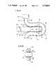
- FIG. 1is a perspective view of a fragmented portion of an integrated circuit substrate showing a jumper cable of the present invention soldered thereto.
- FIG. 2is a side elevation view of the jumper cable of the present invention in accordance with a particular embodiment.
- FIG. 3is a top plan view of the jumper cable of FIG. 2 showing one of the conductors in phantom view.
- FIG. 4is an enlarged fragmentary view of the clip portion of the jumper cable showing the details of the solder connection to the integrated circuit substrate.
- FIG. 5is a cross-sectional view of the solder connection of FIG. 4 as seen along viewing lines V--V.
- FIG. 1a substrate assembly 10 which includes an integrated substrate 12 and a multiconductor jumper cable 14 soldered thereto.
- Substrate 12is formed of an insulative material that may comprise ceramic, fiberglass or other known materials used for supporting integrated circuits.
- the substrate 12comprises a plurality of conductive pads 16 conventionally applied to the substrate adjacent its edges conductive pads 16 being suitably spaced from each other. Pads 16 are disposed on both opposing surfaces 12a and 12b of the substrate 12.
- Cable 14comprises a plurality of elongate electrical conductors 18 extending substantially parallel to and transversely spaced from each other.
- the conductorsare fully surrounded by an insulative casing 20, such as polyester or other suitable insulative material.
- the portions of the conductors 18 that lie interiorly of the insulative casing 20are flattened in a manner to increase the flexibility of the jumper cable.
- the insulative casing 20is laminated onto the conductors 18.
- the flattened portionsare preferably formed in a manner as set forth in commonly assigned, above-mentioned U.S. Pat. No. 3,601,755.
- the electrical conductors inclusive of the pin-like contacts 18a and the clip portions 18bare formed of copper or other suitable non-resilient metal.
- the exposed contacts 18a and clip portions 18bare also suitably coated with a tin plating although other materials such as gold may be suitably placed thereon.
- the curved clip portions 18bare formed to have a substantially circular cross section, the purpose and benefits of which will be hereinafter described. It should also be understood, that while in the particular embodiment described herein the jumper cable includes straight pin-like contacts 18a, the jumper cable 14 may also include curved clipped portions 18b on both ends of the cable 14.
- Each clip portion 18bcomprises a generally U-shaped configuration having opposing legs 18c and 18d.
- the legs of the U-shaped configurationare integrally joined by a curved bridging portion 18e.
- the legs 18c and 18d and the bridging portion 18ddefine a pocket 22 for receipt of the edge portion of the substrate 12 therein.
- the opposing legs 18c and 18ddefine a throat 24 where the legs 18c and 18d are spaced closer together than the legs 18c and 18d at a location 26 near the bottom of the pocket 22 adjacent the bridging portion 18e.
- the spacing of the throat 24is configured to provide an initial interference fit with the substrate 12 during insertion into the pocket 22.
- the conductive pads 16 on the opposing surfaces 12a and 12b of the substrateengage the opposing legs 18c and 18d and slide therealong until the edge of the substrate 12 bottoms out in the pocket 22.
- the material of the clip portion 18bis made of relatively soft copper and is relatively non-resilent, while the initial engagement of the legs 18c and 18d against the conductive pads 16 on the substrate may be in an interference fit, the legs 18c and 18d will not provide a sufficient enough resilient force for an electrical pressure connection. There will be enough force however to position the clip portions 18 on the substrate and hold the clips thereon for subsequent soldering.
- solder connectionis readily provided by a vapor phase soldering, reflow soldering or other conventional technique of soldering to form a permanent joint.
- solderwill form a fillets 28 on both sides of the contact points of the legs 18c and 18d to the conductive pads 16. Also, as illustrated in FIG. 4, as the spacing 26 at the bottom of the pocket 22 between the legs 18c and 18d is greater than the spacing of the throat 24, solder fillets 30 will be formed on both sides of the contact points that the legs 18c and 18d form with the conductive pads 16 at the throat 24.
- the double solder fillets 28 and 30result in an electrical connection that is highly reliable.
- mechanical connectionis also enhanced in such a manner that the solder joint closest of the insulative casing 20 is believed to provide a strain relief for the conductors 18.
- Such strain reliefallows for greater bending adjacent the solder joint than a connection normally provided by a straight pin-like contact.
- the conductors 18may be formed of the relatively soft copper material which as described hereinabove is advantageous in being able to provide a flexible jumper cable that has flattened sections interiorly of the casing 20.
Landscapes
- Engineering & Computer Science (AREA)
- Manufacturing & Machinery (AREA)
- Microelectronics & Electronic Packaging (AREA)
- Multi-Conductor Connections (AREA)
- Coupling Device And Connection With Printed Circuit (AREA)
Abstract
Description
Claims (4)
Priority Applications (2)
| Application Number | Priority Date | Filing Date | Title |
|---|---|---|---|
| US06/859,105US4718863A (en) | 1986-05-02 | 1986-05-02 | Jumper cable having clips for solder connections |
| JP1987065330UJPH025495Y2 (en) | 1986-05-02 | 1987-05-01 |
Applications Claiming Priority (1)
| Application Number | Priority Date | Filing Date | Title |
|---|---|---|---|
| US06/859,105US4718863A (en) | 1986-05-02 | 1986-05-02 | Jumper cable having clips for solder connections |
Publications (1)
| Publication Number | Publication Date |
|---|---|
| US4718863Atrue US4718863A (en) | 1988-01-12 |
Family
ID=25330044
Family Applications (1)
| Application Number | Title | Priority Date | Filing Date |
|---|---|---|---|
| US06/859,105Expired - LifetimeUS4718863A (en) | 1986-05-02 | 1986-05-02 | Jumper cable having clips for solder connections |
Country Status (2)
| Country | Link |
|---|---|
| US (1) | US4718863A (en) |
| JP (1) | JPH025495Y2 (en) |
Cited By (10)
| Publication number | Priority date | Publication date | Assignee | Title |
|---|---|---|---|---|
| US4900279A (en)* | 1989-04-24 | 1990-02-13 | Die Tech, Inc. | Solder terminal |
| US5411420A (en)* | 1993-05-27 | 1995-05-02 | Die Tech, Inc. | Solder terminal strip |
| USRE35549E (en)* | 1991-02-26 | 1997-07-01 | North American Specialties Corporation | Solderable lead |
| EP1083627A1 (en)* | 1999-09-09 | 2001-03-14 | Molex Incorporated | Electrical connector assembly |
| US20040033717A1 (en)* | 2002-08-13 | 2004-02-19 | Fred Peng | Connecting device for connecting electrically a flexible printed board to a circuit board |
| US20050079763A1 (en)* | 1996-10-10 | 2005-04-14 | Lemke Timothy A. | High density connector and method of manufacture |
| US20070184703A1 (en)* | 2002-04-04 | 2007-08-09 | Kim Kyung T | Low voltage electricity distribution circuit |
| WO2007095249A3 (en)* | 2006-02-13 | 2008-06-26 | Kyung T Kim | Electricity distribution circuit |
| US20090260862A1 (en)* | 2008-04-16 | 2009-10-22 | Andrew Yaung | Circuit modification device for printed circuit boards |
| EP2581987A1 (en)* | 2011-10-13 | 2013-04-17 | Valeo Systèmes de Contrôle Moteur | Device for electrical interconnection of at least two electronic cards |
Citations (15)
| Publication number | Priority date | Publication date | Assignee | Title |
|---|---|---|---|---|
| US2457831A (en)* | 1943-06-09 | 1949-01-04 | Pierce John B Foundation | Electricity conductor unit |
| US3102767A (en)* | 1960-12-08 | 1963-09-03 | Kent Mfg Co | Electrical connector for flat conductor cable |
| US3138675A (en)* | 1961-06-07 | 1964-06-23 | Krone Gmbh | Separating and testing plug contact, particularly for separating soldering tag strips in telecommunication technique |
| US3319216A (en)* | 1965-03-25 | 1967-05-09 | Fischer & Porter Co | Connector for flat cables |
| US3401369A (en)* | 1966-06-07 | 1968-09-10 | Ibm | Connector |
| US3601755A (en)* | 1965-12-10 | 1971-08-24 | Digital Sensors Inc | Electrical jumper and method of making same |
| US3728661A (en)* | 1970-03-12 | 1973-04-17 | Honeywell Inf Systems | Modular cabling system |
| US3806767A (en)* | 1973-03-15 | 1974-04-23 | Tek Wave Inc | Interboard connector |
| JPS5013372A (en)* | 1973-04-26 | 1975-02-12 | ||
| US3920301A (en)* | 1972-11-28 | 1975-11-18 | Amp Inc | Electrical connectors for flat cable and methods of making same |
| US3997229A (en)* | 1975-09-15 | 1976-12-14 | Thomas & Betts Corporation | Flexible connecting means |
| US4064622A (en)* | 1976-04-30 | 1977-12-27 | Teledyne Electro Mechanisms | Method of making a flexible jumper strip |
| US4187606A (en)* | 1978-05-08 | 1980-02-12 | Aries Electronics, Inc. | Flexible electrical jumper and method of making same |
| US4556276A (en)* | 1983-05-06 | 1985-12-03 | At&T Bell Laboratories | Solder beams leads |
| US4602316A (en)* | 1985-03-29 | 1986-07-22 | Rca Corporation | Structure and method for interconnecting printed circuit boards |
- 1986
- 1986-05-02USUS06/859,105patent/US4718863A/ennot_activeExpired - Lifetime
- 1987
- 1987-05-01JPJP1987065330Upatent/JPH025495Y2/janot_activeExpired
Patent Citations (15)
| Publication number | Priority date | Publication date | Assignee | Title |
|---|---|---|---|---|
| US2457831A (en)* | 1943-06-09 | 1949-01-04 | Pierce John B Foundation | Electricity conductor unit |
| US3102767A (en)* | 1960-12-08 | 1963-09-03 | Kent Mfg Co | Electrical connector for flat conductor cable |
| US3138675A (en)* | 1961-06-07 | 1964-06-23 | Krone Gmbh | Separating and testing plug contact, particularly for separating soldering tag strips in telecommunication technique |
| US3319216A (en)* | 1965-03-25 | 1967-05-09 | Fischer & Porter Co | Connector for flat cables |
| US3601755A (en)* | 1965-12-10 | 1971-08-24 | Digital Sensors Inc | Electrical jumper and method of making same |
| US3401369A (en)* | 1966-06-07 | 1968-09-10 | Ibm | Connector |
| US3728661A (en)* | 1970-03-12 | 1973-04-17 | Honeywell Inf Systems | Modular cabling system |
| US3920301A (en)* | 1972-11-28 | 1975-11-18 | Amp Inc | Electrical connectors for flat cable and methods of making same |
| US3806767A (en)* | 1973-03-15 | 1974-04-23 | Tek Wave Inc | Interboard connector |
| JPS5013372A (en)* | 1973-04-26 | 1975-02-12 | ||
| US3997229A (en)* | 1975-09-15 | 1976-12-14 | Thomas & Betts Corporation | Flexible connecting means |
| US4064622A (en)* | 1976-04-30 | 1977-12-27 | Teledyne Electro Mechanisms | Method of making a flexible jumper strip |
| US4187606A (en)* | 1978-05-08 | 1980-02-12 | Aries Electronics, Inc. | Flexible electrical jumper and method of making same |
| US4556276A (en)* | 1983-05-06 | 1985-12-03 | At&T Bell Laboratories | Solder beams leads |
| US4602316A (en)* | 1985-03-29 | 1986-07-22 | Rca Corporation | Structure and method for interconnecting printed circuit boards |
Cited By (18)
| Publication number | Priority date | Publication date | Assignee | Title |
|---|---|---|---|---|
| US4900279A (en)* | 1989-04-24 | 1990-02-13 | Die Tech, Inc. | Solder terminal |
| USRE35549E (en)* | 1991-02-26 | 1997-07-01 | North American Specialties Corporation | Solderable lead |
| US5411420A (en)* | 1993-05-27 | 1995-05-02 | Die Tech, Inc. | Solder terminal strip |
| US20080032524A1 (en)* | 1996-10-10 | 2008-02-07 | Lemke Timothy A | High Density Connector and Method of Manufacture |
| US8167630B2 (en) | 1996-10-10 | 2012-05-01 | Fci Americas Technology Llc | High density connector and method of manufacture |
| US20050079763A1 (en)* | 1996-10-10 | 2005-04-14 | Lemke Timothy A. | High density connector and method of manufacture |
| US7186123B2 (en) | 1996-10-10 | 2007-03-06 | Fci Americas Technology, Inc. | High density connector and method of manufacture |
| US7476110B2 (en) | 1996-10-10 | 2009-01-13 | Fci Americas Technology, Inc. | High density connector and method of manufacture |
| EP1083627A1 (en)* | 1999-09-09 | 2001-03-14 | Molex Incorporated | Electrical connector assembly |
| US7547221B2 (en) | 2002-04-04 | 2009-06-16 | Kim Kyung T | Low voltage electricity distribution circuit |
| US20070184703A1 (en)* | 2002-04-04 | 2007-08-09 | Kim Kyung T | Low voltage electricity distribution circuit |
| US20040203274A1 (en)* | 2002-08-13 | 2004-10-14 | Fred Peng | Connecting device for connecting electrically a flexible printed board to a circuit board |
| US20040033717A1 (en)* | 2002-08-13 | 2004-02-19 | Fred Peng | Connecting device for connecting electrically a flexible printed board to a circuit board |
| WO2007095249A3 (en)* | 2006-02-13 | 2008-06-26 | Kyung T Kim | Electricity distribution circuit |
| US20090203242A1 (en)* | 2006-02-13 | 2009-08-13 | Kim Kyung T | Electricity distribution circuit |
| US7789686B2 (en) | 2006-02-13 | 2010-09-07 | Kyung T Kim | Receptacle with three circuit forming apertures |
| US20090260862A1 (en)* | 2008-04-16 | 2009-10-22 | Andrew Yaung | Circuit modification device for printed circuit boards |
| EP2581987A1 (en)* | 2011-10-13 | 2013-04-17 | Valeo Systèmes de Contrôle Moteur | Device for electrical interconnection of at least two electronic cards |
Also Published As
| Publication number | Publication date |
|---|---|
| JPS62180874U (en) | 1987-11-17 |
| JPH025495Y2 (en) | 1990-02-09 |
Similar Documents
| Publication | Publication Date | Title |
|---|---|---|
| US4647126A (en) | Compliant lead clip | |
| KR950012463B1 (en) | Method of manufacturing contact strip and rim clip connector | |
| EP0004148B1 (en) | Electrical connector for use in mounting an electronic device on a substrate | |
| US5041015A (en) | Electrical jumper assembly | |
| US3713072A (en) | Electrical connections to flat conductor cable | |
| JP3330387B2 (en) | Flexible multilayer circuit wiring board | |
| US3754203A (en) | Substrate connector and terminal therefore | |
| US4385791A (en) | Electrical adaptor block | |
| US4192565A (en) | Multi-level socket for an integrated circuit | |
| JPS6231836B2 (en) | ||
| EP0017358B1 (en) | Electrical connector housing with a mounting peg | |
| US4718863A (en) | Jumper cable having clips for solder connections | |
| US4668032A (en) | Flexible solder socket for connecting leadless integrated circuit packages to a printed circuit board | |
| GB2202682A (en) | Connection leads for surface mounted components | |
| JPS5998591A (en) | Double-sided circuit connection method | |
| US4869671A (en) | Electrical connector for printed circuit board | |
| US5049089A (en) | Low cost arch connector | |
| JP3341894B2 (en) | Holders for electrical and / or electronic components | |
| JPS62188181A (en) | Surface mount connector | |
| US3290637A (en) | Microelectronic module assembly | |
| US3410952A (en) | Electrical bus strip | |
| JPH0661609A (en) | Circuit board | |
| JPH07153535A (en) | Method for connecting electric component and printed circuit board and terminal for connecting the same | |
| US4580857A (en) | Circuit terminating clip | |
| KR0118721Y1 (en) | Electrical connector |
Legal Events
| Date | Code | Title | Description |
|---|---|---|---|
| AS | Assignment | Owner name:THOMAS & BETTS CORPORATION, 920 ROUTE 202, RARITAN Free format text:ASSIGNMENT OF ASSIGNORS INTEREST.;ASSIGNOR:SADIGH-BEHZADI, AMIR-AKBAR;REEL/FRAME:004555/0528 Effective date:19860429 Owner name:THOMAS & BETTS CORPORATION,NEW YORK Free format text:ASSIGNMENT OF ASSIGNORS INTEREST;ASSIGNOR:SADIGH-BEHZADI, AMIR-AKBAR;REEL/FRAME:004555/0528 Effective date:19860429 | |
| STCF | Information on status: patent grant | Free format text:PATENTED CASE | |
| FEPP | Fee payment procedure | Free format text:PAYOR NUMBER ASSIGNED (ORIGINAL EVENT CODE: ASPN); ENTITY STATUS OF PATENT OWNER: LARGE ENTITY | |
| FPAY | Fee payment | Year of fee payment:4 | |
| FPAY | Fee payment | Year of fee payment:8 | |
| AS | Assignment | Owner name:THOMAS & BETTS INTERNATIONAL, INC., NEVADA Free format text:ASSIGNMENT OF ASSIGNORS INTEREST;ASSIGNOR:THOMAS & BETTS CORPORATION;REEL/FRAME:009534/0734 Effective date:19981007 | |
| FPAY | Fee payment | Year of fee payment:12 | |
| FEPP | Fee payment procedure | Free format text:PAYER NUMBER DE-ASSIGNED (ORIGINAL EVENT CODE: RMPN); ENTITY STATUS OF PATENT OWNER: LARGE ENTITY Free format text:PAYOR NUMBER ASSIGNED (ORIGINAL EVENT CODE: ASPN); ENTITY STATUS OF PATENT OWNER: LARGE ENTITY |