US4717066A - Method of bonding conductors to semiconductor devices - Google Patents
Method of bonding conductors to semiconductor devicesDownload PDFInfo
- Publication number
- US4717066A US4717066AUS06/831,814US83181486AUS4717066AUS 4717066 AUS4717066 AUS 4717066AUS 83181486 AUS83181486 AUS 83181486AUS 4717066 AUS4717066 AUS 4717066A
- Authority
- US
- United States
- Prior art keywords
- wire
- ball
- bonding
- pad
- forming
- Prior art date
- Legal status (The legal status is an assumption and is not a legal conclusion. Google has not performed a legal analysis and makes no representation as to the accuracy of the status listed.)
- Expired - Lifetime
Links
Images
Classifications
- H—ELECTRICITY
- H01—ELECTRIC ELEMENTS
- H01L—SEMICONDUCTOR DEVICES NOT COVERED BY CLASS H10
- H01L23/00—Details of semiconductor or other solid state devices
- H01L23/48—Arrangements for conducting electric current to or from the solid state body in operation, e.g. leads, terminal arrangements ; Selection of materials therefor
- H01L23/488—Arrangements for conducting electric current to or from the solid state body in operation, e.g. leads, terminal arrangements ; Selection of materials therefor consisting of soldered or bonded constructions
- H01L23/495—Lead-frames or other flat leads
- H01L23/49517—Additional leads
- H01L23/4952—Additional leads the additional leads being a bump or a wire
- B—PERFORMING OPERATIONS; TRANSPORTING
- B23—MACHINE TOOLS; METAL-WORKING NOT OTHERWISE PROVIDED FOR
- B23K—SOLDERING OR UNSOLDERING; WELDING; CLADDING OR PLATING BY SOLDERING OR WELDING; CUTTING BY APPLYING HEAT LOCALLY, e.g. FLAME CUTTING; WORKING BY LASER BEAM
- B23K20/00—Non-electric welding by applying impact or other pressure, with or without the application of heat, e.g. cladding or plating
- B23K20/002—Non-electric welding by applying impact or other pressure, with or without the application of heat, e.g. cladding or plating specially adapted for particular articles or work
- B23K20/004—Wire welding
- B23K20/005—Capillary welding
- B23K20/007—Ball bonding
- H—ELECTRICITY
- H01—ELECTRIC ELEMENTS
- H01L—SEMICONDUCTOR DEVICES NOT COVERED BY CLASS H10
- H01L24/00—Arrangements for connecting or disconnecting semiconductor or solid-state bodies; Methods or apparatus related thereto
- H01L24/01—Means for bonding being attached to, or being formed on, the surface to be connected, e.g. chip-to-package, die-attach, "first-level" interconnects; Manufacturing methods related thereto
- H01L24/10—Bump connectors ; Manufacturing methods related thereto
- H01L24/11—Manufacturing methods
- H—ELECTRICITY
- H01—ELECTRIC ELEMENTS
- H01L—SEMICONDUCTOR DEVICES NOT COVERED BY CLASS H10
- H01L24/00—Arrangements for connecting or disconnecting semiconductor or solid-state bodies; Methods or apparatus related thereto
- H01L24/01—Means for bonding being attached to, or being formed on, the surface to be connected, e.g. chip-to-package, die-attach, "first-level" interconnects; Manufacturing methods related thereto
- H01L24/10—Bump connectors ; Manufacturing methods related thereto
- H01L24/15—Structure, shape, material or disposition of the bump connectors after the connecting process
- H01L24/16—Structure, shape, material or disposition of the bump connectors after the connecting process of an individual bump connector
- H—ELECTRICITY
- H01—ELECTRIC ELEMENTS
- H01L—SEMICONDUCTOR DEVICES NOT COVERED BY CLASS H10
- H01L24/00—Arrangements for connecting or disconnecting semiconductor or solid-state bodies; Methods or apparatus related thereto
- H01L24/01—Means for bonding being attached to, or being formed on, the surface to be connected, e.g. chip-to-package, die-attach, "first-level" interconnects; Manufacturing methods related thereto
- H01L24/50—Tape automated bonding [TAB] connectors, i.e. film carriers; Manufacturing methods related thereto
- H—ELECTRICITY
- H01—ELECTRIC ELEMENTS
- H01L—SEMICONDUCTOR DEVICES NOT COVERED BY CLASS H10
- H01L24/00—Arrangements for connecting or disconnecting semiconductor or solid-state bodies; Methods or apparatus related thereto
- H01L24/80—Methods for connecting semiconductor or other solid state bodies using means for bonding being attached to, or being formed on, the surface to be connected
- H01L24/81—Methods for connecting semiconductor or other solid state bodies using means for bonding being attached to, or being formed on, the surface to be connected using a bump connector
- H—ELECTRICITY
- H01—ELECTRIC ELEMENTS
- H01L—SEMICONDUCTOR DEVICES NOT COVERED BY CLASS H10
- H01L24/00—Arrangements for connecting or disconnecting semiconductor or solid-state bodies; Methods or apparatus related thereto
- H01L24/80—Methods for connecting semiconductor or other solid state bodies using means for bonding being attached to, or being formed on, the surface to be connected
- H01L24/86—Methods for connecting semiconductor or other solid state bodies using means for bonding being attached to, or being formed on, the surface to be connected using tape automated bonding [TAB]
- H—ELECTRICITY
- H01—ELECTRIC ELEMENTS
- H01L—SEMICONDUCTOR DEVICES NOT COVERED BY CLASS H10
- H01L2224/00—Indexing scheme for arrangements for connecting or disconnecting semiconductor or solid-state bodies and methods related thereto as covered by H01L24/00
- H01L2224/01—Means for bonding being attached to, or being formed on, the surface to be connected, e.g. chip-to-package, die-attach, "first-level" interconnects; Manufacturing methods related thereto
- H01L2224/02—Bonding areas; Manufacturing methods related thereto
- H01L2224/04—Structure, shape, material or disposition of the bonding areas prior to the connecting process
- H01L2224/05—Structure, shape, material or disposition of the bonding areas prior to the connecting process of an individual bonding area
- H01L2224/0554—External layer
- H01L2224/05599—Material
- H01L2224/056—Material with a principal constituent of the material being a metal or a metalloid, e.g. boron [B], silicon [Si], germanium [Ge], arsenic [As], antimony [Sb], tellurium [Te] and polonium [Po], and alloys thereof
- H01L2224/05617—Material with a principal constituent of the material being a metal or a metalloid, e.g. boron [B], silicon [Si], germanium [Ge], arsenic [As], antimony [Sb], tellurium [Te] and polonium [Po], and alloys thereof the principal constituent melting at a temperature of greater than or equal to 400°C and less than 950°C
- H01L2224/05624—Aluminium [Al] as principal constituent
- H—ELECTRICITY
- H01—ELECTRIC ELEMENTS
- H01L—SEMICONDUCTOR DEVICES NOT COVERED BY CLASS H10
- H01L2224/00—Indexing scheme for arrangements for connecting or disconnecting semiconductor or solid-state bodies and methods related thereto as covered by H01L24/00
- H01L2224/01—Means for bonding being attached to, or being formed on, the surface to be connected, e.g. chip-to-package, die-attach, "first-level" interconnects; Manufacturing methods related thereto
- H01L2224/10—Bump connectors; Manufacturing methods related thereto
- H01L2224/11—Manufacturing methods
- H01L2224/113—Manufacturing methods by local deposition of the material of the bump connector
- H01L2224/1133—Manufacturing methods by local deposition of the material of the bump connector in solid form
- H01L2224/1134—Stud bumping, i.e. using a wire-bonding apparatus
- H—ELECTRICITY
- H01—ELECTRIC ELEMENTS
- H01L—SEMICONDUCTOR DEVICES NOT COVERED BY CLASS H10
- H01L2224/00—Indexing scheme for arrangements for connecting or disconnecting semiconductor or solid-state bodies and methods related thereto as covered by H01L24/00
- H01L2224/01—Means for bonding being attached to, or being formed on, the surface to be connected, e.g. chip-to-package, die-attach, "first-level" interconnects; Manufacturing methods related thereto
- H01L2224/10—Bump connectors; Manufacturing methods related thereto
- H01L2224/12—Structure, shape, material or disposition of the bump connectors prior to the connecting process
- H01L2224/13—Structure, shape, material or disposition of the bump connectors prior to the connecting process of an individual bump connector
- H01L2224/13001—Core members of the bump connector
- H01L2224/13099—Material
- H01L2224/131—Material with a principal constituent of the material being a metal or a metalloid, e.g. boron [B], silicon [Si], germanium [Ge], arsenic [As], antimony [Sb], tellurium [Te] and polonium [Po], and alloys thereof
- H01L2224/13138—Material with a principal constituent of the material being a metal or a metalloid, e.g. boron [B], silicon [Si], germanium [Ge], arsenic [As], antimony [Sb], tellurium [Te] and polonium [Po], and alloys thereof the principal constituent melting at a temperature of greater than or equal to 950°C and less than 1550°C
- H01L2224/13144—Gold [Au] as principal constituent
- H—ELECTRICITY
- H01—ELECTRIC ELEMENTS
- H01L—SEMICONDUCTOR DEVICES NOT COVERED BY CLASS H10
- H01L2224/00—Indexing scheme for arrangements for connecting or disconnecting semiconductor or solid-state bodies and methods related thereto as covered by H01L24/00
- H01L2224/01—Means for bonding being attached to, or being formed on, the surface to be connected, e.g. chip-to-package, die-attach, "first-level" interconnects; Manufacturing methods related thereto
- H01L2224/10—Bump connectors; Manufacturing methods related thereto
- H01L2224/15—Structure, shape, material or disposition of the bump connectors after the connecting process
- H01L2224/16—Structure, shape, material or disposition of the bump connectors after the connecting process of an individual bump connector
- H—ELECTRICITY
- H01—ELECTRIC ELEMENTS
- H01L—SEMICONDUCTOR DEVICES NOT COVERED BY CLASS H10
- H01L2224/00—Indexing scheme for arrangements for connecting or disconnecting semiconductor or solid-state bodies and methods related thereto as covered by H01L24/00
- H01L2224/74—Apparatus for manufacturing arrangements for connecting or disconnecting semiconductor or solid-state bodies and for methods related thereto
- H01L2224/78—Apparatus for connecting with wire connectors
- H01L2224/7825—Means for applying energy, e.g. heating means
- H01L2224/783—Means for applying energy, e.g. heating means by means of pressure
- H01L2224/78301—Capillary
- H—ELECTRICITY
- H01—ELECTRIC ELEMENTS
- H01L—SEMICONDUCTOR DEVICES NOT COVERED BY CLASS H10
- H01L2224/00—Indexing scheme for arrangements for connecting or disconnecting semiconductor or solid-state bodies and methods related thereto as covered by H01L24/00
- H01L2224/80—Methods for connecting semiconductor or other solid state bodies using means for bonding being attached to, or being formed on, the surface to be connected
- H01L2224/81—Methods for connecting semiconductor or other solid state bodies using means for bonding being attached to, or being formed on, the surface to be connected using a bump connector
- H01L2224/812—Applying energy for connecting
- H01L2224/81201—Compression bonding
- H01L2224/81203—Thermocompression bonding, e.g. diffusion bonding, pressure joining, thermocompression welding or solid-state welding
- H—ELECTRICITY
- H01—ELECTRIC ELEMENTS
- H01L—SEMICONDUCTOR DEVICES NOT COVERED BY CLASS H10
- H01L2224/00—Indexing scheme for arrangements for connecting or disconnecting semiconductor or solid-state bodies and methods related thereto as covered by H01L24/00
- H01L2224/80—Methods for connecting semiconductor or other solid state bodies using means for bonding being attached to, or being formed on, the surface to be connected
- H01L2224/81—Methods for connecting semiconductor or other solid state bodies using means for bonding being attached to, or being formed on, the surface to be connected using a bump connector
- H01L2224/818—Bonding techniques
- H01L2224/81801—Soldering or alloying
- H—ELECTRICITY
- H01—ELECTRIC ELEMENTS
- H01L—SEMICONDUCTOR DEVICES NOT COVERED BY CLASS H10
- H01L2924/00—Indexing scheme for arrangements or methods for connecting or disconnecting semiconductor or solid-state bodies as covered by H01L24/00
- H01L2924/01—Chemical elements
- H01L2924/01004—Beryllium [Be]
- H—ELECTRICITY
- H01—ELECTRIC ELEMENTS
- H01L—SEMICONDUCTOR DEVICES NOT COVERED BY CLASS H10
- H01L2924/00—Indexing scheme for arrangements or methods for connecting or disconnecting semiconductor or solid-state bodies as covered by H01L24/00
- H01L2924/01—Chemical elements
- H01L2924/01006—Carbon [C]
- H—ELECTRICITY
- H01—ELECTRIC ELEMENTS
- H01L—SEMICONDUCTOR DEVICES NOT COVERED BY CLASS H10
- H01L2924/00—Indexing scheme for arrangements or methods for connecting or disconnecting semiconductor or solid-state bodies as covered by H01L24/00
- H01L2924/01—Chemical elements
- H01L2924/01013—Aluminum [Al]
- H—ELECTRICITY
- H01—ELECTRIC ELEMENTS
- H01L—SEMICONDUCTOR DEVICES NOT COVERED BY CLASS H10
- H01L2924/00—Indexing scheme for arrangements or methods for connecting or disconnecting semiconductor or solid-state bodies as covered by H01L24/00
- H01L2924/01—Chemical elements
- H01L2924/01029—Copper [Cu]
- H—ELECTRICITY
- H01—ELECTRIC ELEMENTS
- H01L—SEMICONDUCTOR DEVICES NOT COVERED BY CLASS H10
- H01L2924/00—Indexing scheme for arrangements or methods for connecting or disconnecting semiconductor or solid-state bodies as covered by H01L24/00
- H01L2924/01—Chemical elements
- H01L2924/01033—Arsenic [As]
- H—ELECTRICITY
- H01—ELECTRIC ELEMENTS
- H01L—SEMICONDUCTOR DEVICES NOT COVERED BY CLASS H10
- H01L2924/00—Indexing scheme for arrangements or methods for connecting or disconnecting semiconductor or solid-state bodies as covered by H01L24/00
- H01L2924/01—Chemical elements
- H01L2924/01046—Palladium [Pd]
- H—ELECTRICITY
- H01—ELECTRIC ELEMENTS
- H01L—SEMICONDUCTOR DEVICES NOT COVERED BY CLASS H10
- H01L2924/00—Indexing scheme for arrangements or methods for connecting or disconnecting semiconductor or solid-state bodies as covered by H01L24/00
- H01L2924/01—Chemical elements
- H01L2924/01079—Gold [Au]
- H—ELECTRICITY
- H01—ELECTRIC ELEMENTS
- H01L—SEMICONDUCTOR DEVICES NOT COVERED BY CLASS H10
- H01L2924/00—Indexing scheme for arrangements or methods for connecting or disconnecting semiconductor or solid-state bodies as covered by H01L24/00
- H01L2924/01—Chemical elements
- H01L2924/01082—Lead [Pb]
Definitions
- This inventionrelates to formation of electrical contacts to semiconductor devices.
- Tape automated bondingis one method of forming electrical connections to contact pads on a semiconductor device or circuit.
- the techniquebasically involves formation of conductive leads on a tape backing and then bonding the leads to the contact pads on the semiconductor by means of spheres or bumps initially attached to either the pads or the tape leads.
- the spheres or bumpshereinafter also referred to as contact portions, act as buffers to absorb the impact of bonding the leads to the pads.
- the opposite ends of the leadscan then be coupled to external circuitry.
- TABprovides many advantages over standard techniques, such as wire bonding to lead frames, used in semiconductor fabrication. For example, since TAB leads can usually be made thicker than wire bonded interconnections, the technique generally produces less noise in high frequency applications. Further, since the TAB leads can also be made with a higher density than wire bonded interconnections, TAB is useful in devices requiring a high density of electrical connection to the semiconductor chip due to either a great number of required connections or reduced pad and chip sizes.
- TABhas not been employed widely in MOS devices or circuits. This is primarily due to the fact that it has been difficult to form a strong bond between the contact portions and the aluminum pad metallization commonly employed in such devices.
- One method proposed for establishing a bond between a bump or sphere and the semiconductor contact padis to ball-bond a wire to the pad in a manner similar to wire bonding techniques, and then sever the wire above the ball by weakening the wire either through mechanical manipulation or through formation of a coarse crystalline structure above the ball.
- wire bonding techniquesSee U.S. Pat. No. 4,442,967 issued to van de Pas, which is incorporated by reference herein.
- the inventionin one aspect is a method of forming a contact portion on a metal pad.
- the methodincludes the steps of forming a ball on one end of a wire, bonding the ball to the metal pad, and severing the wire from the ball.
- the wire materialcomprises gold and palladium.
- the inventionis an MOS semiconductor device comprising a semiconductor substrate, a metal pad formed over the substrate, a contact portion bonded to the metal pad, and a conductive lead supported by an insulating tape and bonded to the contact portion.
- the contact portionis a material comprising gold and palladium.
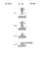
- FIGS. 1-4are cross-sectional schematic views representing different steps in the practice of the invention in accordance with one embodiment.
- FIGS. 1-4The basic features of the invention will be described with reference to the embodiment shown in the sequence of steps illustrated in FIGS. 1-4.
- the figuresdemonstrate the formation of an electrical contact to one pad, 11, situated on a major surface of a semiconductor substrate, 10.
- the substratewill include several such pads on the periphery of at least one side of the substrate and other elements formed on the surface and within the semiconductor material. For the sake of clarity in the illustration, these additional pads and features have been omitted.
- the pad, 11,was aluminum with a thickness of approximately 1 micron, and measured 100 microns ⁇ 100 microns.
- the semiconductor substrate, 10,included a standard MOS circuit and measured approximately 200 mils ⁇ 200 mils ⁇ 20 mils.
- a wire, 12,was held within a capillary tube, 14, in a manner similar to U.S. Pat. No. 4,442,967, previously cited.
- the capillary tubewas part of a standard apparatus commonly employed for wire bonding to semiconductor chip pads and so is not shown. In this example, the apparatus was sold by Kolicke and Soffa Industries under the designation Model 1419.
- the wirehad a diameter of approximately 1 mil.
- the wire materialwas a gold alloy which was found to have particularly desirable properties in the practice of the method as discussed below.
- the materialwas approximately 99 percent gold and 1 percent palladium.
- a ball, 13was formed in accordance with standard ball-bonding techniques. This involved heating the wire, above its melting point by an electrostatic discharge as commonly employed in the art.
- the ball, 13,was then brought into physical contact with the pad, 11, for the purpose of bonding thereto.
- a thermosonic bonding operationwas then performed with approximately 50 grams pressure applied to the ball and heat supplied to the wire and ball by some such as a heated pedestal which supports the substrate in accordance with standard practice.
- the heating stepwas performed at a higher temperature than normally employed for gold ball-bonding.
- the pedestalwas heated to a surface temperature of approximately 225 degrees C. However, a temperature in the range 175-300 degrees C. should be useful.
- This contact portionincludes the ball 13 and a small stub, 19, from the wire. Because of the weakening of the wire in accordance with the invention, this stub is quite small, typically 2 mils in height, and so does not significantly affect attachment of conductors to the contact portions.
- a conductive lead, 15, formed on a tape 16was bonded to the contact portion 17.
- the leadwas gold-plated copper with a thickness of approximately 1.3 mils and the tape was Kapton with a thickness of approximately 1 mil.
- One end of the leadwas bonded to the contact 17 by thermocompression bonding, leaving the opposite end for attachment to external circuitry as might be present, for example, on a printed circuit board or lead frame.
- wire material described abovewas found to produce desirable results, other wire compositions might be employed.
- the proportion of the palladium in the gold alloycould be varied.
- a useful range for the proportion of palladiumis expected to be 1-3 percent.
- additional materialsmight be incorporated in the gold-palladium alloy, such as beryllium.
- berylliumit may be possible to employ beryllium in sufficient quantity (greater than 1 percent) so that palladium can be eliminated from the composition.
Landscapes
- Engineering & Computer Science (AREA)
- Computer Hardware Design (AREA)
- Microelectronics & Electronic Packaging (AREA)
- Power Engineering (AREA)
- Manufacturing & Machinery (AREA)
- Physics & Mathematics (AREA)
- Condensed Matter Physics & Semiconductors (AREA)
- General Physics & Mathematics (AREA)
- Mechanical Engineering (AREA)
- Wire Bonding (AREA)
Abstract
Description
This invention relates to formation of electrical contacts to semiconductor devices.
Tape automated bonding (TAB) is one method of forming electrical connections to contact pads on a semiconductor device or circuit. The technique basically involves formation of conductive leads on a tape backing and then bonding the leads to the contact pads on the semiconductor by means of spheres or bumps initially attached to either the pads or the tape leads. The spheres or bumps, hereinafter also referred to as contact portions, act as buffers to absorb the impact of bonding the leads to the pads. The opposite ends of the leads can then be coupled to external circuitry.
TAB provides many advantages over standard techniques, such as wire bonding to lead frames, used in semiconductor fabrication. For example, since TAB leads can usually be made thicker than wire bonded interconnections, the technique generally produces less noise in high frequency applications. Further, since the TAB leads can also be made with a higher density than wire bonded interconnections, TAB is useful in devices requiring a high density of electrical connection to the semiconductor chip due to either a great number of required connections or reduced pad and chip sizes.
In spite of such advantages, TAB has not been employed widely in MOS devices or circuits. This is primarily due to the fact that it has been difficult to form a strong bond between the contact portions and the aluminum pad metallization commonly employed in such devices.
One method proposed for establishing a bond between a bump or sphere and the semiconductor contact pad is to ball-bond a wire to the pad in a manner similar to wire bonding techniques, and then sever the wire above the ball by weakening the wire either through mechanical manipulation or through formation of a coarse crystalline structure above the ball. (See U.S. Pat. No. 4,442,967 issued to van de Pas, which is incorporated by reference herein.) While generally adequate for providing a strong bond, such a technique presents some difficulties in reliably severing the wire.
It is therefore an object of the invention to provide strong bonds between contact portions and semiconductor chip bonding pads in a reliable manner so that conductors can be bonded to the contact portions to provide external connection to the chip.
This and other objects are achieved in accordance with the invention which in one aspect is a method of forming a contact portion on a metal pad. The method includes the steps of forming a ball on one end of a wire, bonding the ball to the metal pad, and severing the wire from the ball. The wire material comprises gold and palladium.
In accordance with another aspect, the invention is an MOS semiconductor device comprising a semiconductor substrate, a metal pad formed over the substrate, a contact portion bonded to the metal pad, and a conductive lead supported by an insulating tape and bonded to the contact portion. The contact portion is a material comprising gold and palladium.
These and other features of the invention are delineated in detail in the following description. In the drawing:
FIGS. 1-4 are cross-sectional schematic views representing different steps in the practice of the invention in accordance with one embodiment.
It will be appreciated that for purposes of illustration these figures are not necessarily drawn to scale.
The basic features of the invention will be described with reference to the embodiment shown in the sequence of steps illustrated in FIGS. 1-4. The figures demonstrate the formation of an electrical contact to one pad, 11, situated on a major surface of a semiconductor substrate, 10. It will be appreciated that in actual practice, the substrate will include several such pads on the periphery of at least one side of the substrate and other elements formed on the surface and within the semiconductor material. For the sake of clarity in the illustration, these additional pads and features have been omitted. In this particular example, the pad, 11, was aluminum with a thickness of approximately 1 micron, and measured 100 microns×100 microns. The semiconductor substrate, 10, included a standard MOS circuit and measured approximately 200 mils×200 mils×20 mils.
A wire, 12, was held within a capillary tube, 14, in a manner similar to U.S. Pat. No. 4,442,967, previously cited. The capillary tube was part of a standard apparatus commonly employed for wire bonding to semiconductor chip pads and so is not shown. In this example, the apparatus was sold by Kolicke and Soffa Industries under the designation Model 1419. The wire had a diameter of approximately 1 mil.
In accordance with an important feature of the invention, the wire material was a gold alloy which was found to have particularly desirable properties in the practice of the method as discussed below. In this example, the material was approximately 99 percent gold and 1 percent palladium.
At the tip of the wire, 12, a ball, 13, was formed in accordance with standard ball-bonding techniques. This involved heating the wire, above its melting point by an electrostatic discharge as commonly employed in the art.
As illustrated in FIG. 2, the ball, 13, was then brought into physical contact with the pad, 11, for the purpose of bonding thereto. A thermosonic bonding operation was then performed with approximately 50 grams pressure applied to the ball and heat supplied to the wire and ball by some such as a heated pedestal which supports the substrate in accordance with standard practice. In accordance with a further feature of the invention, the heating step was performed at a higher temperature than normally employed for gold ball-bonding. In this particular example, the pedestal was heated to a surface temperature of approximately 225 degrees C. However, a temperature in the range 175-300 degrees C. should be useful.
It was discovered that use of a gold alloy and an appropriate heating step as described above results not only in a strong between the ball and pad, but also a weakening of the portion, 18, of the wire immediately above the ball. This permits the wire, 12, to be severed from the ball, 13, by pulling on the wire with a simple upward vertical movement of thetube 14.
As illustrated in FIG. 3, after severing the wire, a raised contact portion, 17, is left bonded to the pad. This contact portion includes theball 13 and a small stub, 19, from the wire. Because of the weakening of the wire in accordance with the invention, this stub is quite small, typically 2 mils in height, and so does not significantly affect attachment of conductors to the contact portions.
As shown in FIG. 4, a conductive lead, 15, formed on atape 16, was bonded to the contact portion 17. As is standard in tape automated bonding, the lead was gold-plated copper with a thickness of approximately 1.3 mils and the tape was Kapton with a thickness of approximately 1 mil. One end of the lead was bonded to the contact 17 by thermocompression bonding, leaving the opposite end for attachment to external circuitry as might be present, for example, on a printed circuit board or lead frame.
Although the wire material described above was found to produce desirable results, other wire compositions might be employed. For example, the proportion of the palladium in the gold alloy could be varied. A useful range for the proportion of palladium is expected to be 1-3 percent. Further, additional materials might be incorporated in the gold-palladium alloy, such as beryllium. Further, it may be possible to employ beryllium in sufficient quantity (greater than 1 percent) so that palladium can be eliminated from the composition.
Various additional modifications of the invention will become apparent to those skilled in the art. All such variations which basically rely on the teachings through which the invention has advanced the art are properly considered within the scope of the invention.
Claims (8)
1. A method of forming a contact portion on a metal pad comprising the steps of forming a ball on one end of a conductive wire, bonding the ball to the metal pad and severing the wire from the ball, characterized in that the wire material comprises 97-99 percent gold and 1-3 percent palladium.
2. A method of forming a contact portion on a metal pad comprising the steps of forming a ball on one end of a conductive wire, bonding the ball to the metal and severing the wire from the ball, characterized in that the wire material consists essentially of gold and palladium.
3. The method according to claim 1 or 2 wherein the pad is disposed on a substrate and the substrate is heated to a temperature within the range 175-300 degrees C. during the bonding of the ball to the pad.
4. The method according to claim 1 or 2 wherein the metal pad comprises aluminum.
5. The method according to claim 1 or 2 further comprising bonding a conductive lead supported by an insulating tape onto the contact portion.
6. The method according to claim 1 or 2 wherein the metal pad is formed over a semiconductor substrate.
7. A method of making electrical contact to an MOS semiconductor chip including an aluminum pad on one major surface comprising the steps of:
providing a conductive wire consisting essentially of gold and palladium, and forming a ball on one end of the wire;
bonding the ball to the metal pad by heating the semiconductor substrate in the range 175-300 degrees C. while contacting the ball to the pad;
severing the wire from the ball by pulling on the wire; and
bonding a conductive lead supported by an insulated tape onto the ball.
8. The method according to claim 7 wherein the wire is provided in a support tube and the wire is severed from the ball by only an upward movement of the tube.
Priority Applications (1)
| Application Number | Priority Date | Filing Date | Title |
|---|---|---|---|
| US06/831,814US4717066A (en) | 1986-02-24 | 1986-02-24 | Method of bonding conductors to semiconductor devices |
Applications Claiming Priority (1)
| Application Number | Priority Date | Filing Date | Title |
|---|---|---|---|
| US06/831,814US4717066A (en) | 1986-02-24 | 1986-02-24 | Method of bonding conductors to semiconductor devices |
Publications (1)
| Publication Number | Publication Date |
|---|---|
| US4717066Atrue US4717066A (en) | 1988-01-05 |
Family
ID=25259930
Family Applications (1)
| Application Number | Title | Priority Date | Filing Date |
|---|---|---|---|
| US06/831,814Expired - LifetimeUS4717066A (en) | 1986-02-24 | 1986-02-24 | Method of bonding conductors to semiconductor devices |
Country Status (1)
| Country | Link |
|---|---|
| US (1) | US4717066A (en) |
Cited By (106)
| Publication number | Priority date | Publication date | Assignee | Title |
|---|---|---|---|---|
| US4948030A (en)* | 1989-01-30 | 1990-08-14 | Motorola, Inc. | Bond connection for components |
| EP0320244A3 (en)* | 1987-12-08 | 1990-10-10 | Matsushita Electric Industrial Co. Ltd. | Electrical contact bump and a package provided with the same |
| US4993622A (en)* | 1987-04-28 | 1991-02-19 | Texas Instruments Incorporated | Semiconductor integrated circuit chip interconnections and methods |
| US5060843A (en)* | 1989-06-07 | 1991-10-29 | Nec Corporation | Process of forming bump on electrode of semiconductor chip and apparatus used therefor |
| US5086966A (en)* | 1990-11-05 | 1992-02-11 | Motorola Inc. | Palladium-coated solder ball |
| US5172851A (en)* | 1990-09-20 | 1992-12-22 | Matsushita Electronics Corporation | Method of forming a bump electrode and manufacturing a resin-encapsulated semiconductor device |
| US5249098A (en)* | 1991-08-22 | 1993-09-28 | Lsi Logic Corporation | Semiconductor device package with solder bump electrical connections on an external surface of the package |
| US5299730A (en)* | 1989-08-28 | 1994-04-05 | Lsi Logic Corporation | Method and apparatus for isolation of flux materials in flip-chip manufacturing |
| US5311060A (en)* | 1989-12-19 | 1994-05-10 | Lsi Logic Corporation | Heat sink for semiconductor device assembly |
| US5388327A (en)* | 1993-09-15 | 1995-02-14 | Lsi Logic Corporation | Fabrication of a dissolvable film carrier containing conductive bump contacts for placement on a semiconductor device package |
| US5397997A (en)* | 1991-08-23 | 1995-03-14 | Nchip, Inc. | Burn-in technologies for unpackaged integrated circuits |
| US5399903A (en)* | 1990-08-15 | 1995-03-21 | Lsi Logic Corporation | Semiconductor device having an universal die size inner lead layout |
| US5434750A (en)* | 1992-02-07 | 1995-07-18 | Lsi Logic Corporation | Partially-molded, PCB chip carrier package for certain non-square die shapes |
| US5438477A (en)* | 1993-08-12 | 1995-08-01 | Lsi Logic Corporation | Die-attach technique for flip-chip style mounting of semiconductor dies |
| US5455195A (en)* | 1994-05-06 | 1995-10-03 | Texas Instruments Incorporated | Method for obtaining metallurgical stability in integrated circuit conductive bonds |
| US5541524A (en)* | 1991-08-23 | 1996-07-30 | Nchip, Inc. | Burn-in technologies for unpackaged integrated circuits |
| US5734546A (en)* | 1994-09-21 | 1998-03-31 | Rohm Co. Ltd. | Capacitor element for solid electrolytic capacitor and process for making the same |
| US5747358A (en)* | 1996-05-29 | 1998-05-05 | W. L. Gore & Associates, Inc. | Method of forming raised metallic contacts on electrical circuits |
| US5767580A (en)* | 1993-04-30 | 1998-06-16 | Lsi Logic Corporation | Systems having shaped, self-aligning micro-bump structures |
| US5938105A (en)* | 1997-01-15 | 1999-08-17 | National Semiconductor Corporation | Encapsulated ball bonding apparatus and method |
| US6065667A (en)* | 1997-01-15 | 2000-05-23 | National Semiconductor Corporation | Method and apparatus for fine pitch wire bonding |
| US6096576A (en)* | 1997-09-02 | 2000-08-01 | Silicon Light Machines | Method of producing an electrical interface to an integrated circuit device having high density I/O count |
| US6350632B1 (en) | 2000-09-20 | 2002-02-26 | Charles W. C. Lin | Semiconductor chip assembly with ball bond connection joint |
| US6350386B1 (en) | 2000-09-20 | 2002-02-26 | Charles W. C. Lin | Method of making a support circuit with a tapered through-hole for a semiconductor chip assembly |
| US6440835B1 (en) | 2000-10-13 | 2002-08-27 | Charles W. C. Lin | Method of connecting a conductive trace to a semiconductor chip |
| US6444489B1 (en) | 2000-12-15 | 2002-09-03 | Charles W. C. Lin | Semiconductor chip assembly with bumped molded substrate |
| US6448108B1 (en) | 2000-10-02 | 2002-09-10 | Charles W. C. Lin | Method of making a semiconductor chip assembly with a conductive trace subtractively formed before and after chip attachment |
| US6492252B1 (en) | 2000-10-13 | 2002-12-10 | Bridge Semiconductor Corporation | Method of connecting a bumped conductive trace to a semiconductor chip |
| US6511865B1 (en) | 2000-09-20 | 2003-01-28 | Charles W. C. Lin | Method for forming a ball bond connection joint on a conductive trace and conductive pad in a semiconductor chip assembly |
| US20030038943A1 (en)* | 2001-08-21 | 2003-02-27 | Kais Almarzouk | Method and apparatus for measuring wavelength jitter of light signal |
| US6537851B1 (en) | 2000-10-13 | 2003-03-25 | Bridge Semiconductor Corporation | Method of connecting a bumped compliant conductive trace to a semiconductor chip |
| US6544813B1 (en) | 2000-10-02 | 2003-04-08 | Charles W. C. Lin | Method of making a semiconductor chip assembly with a conductive trace subtractively formed before and after chip attachment |
| US6548393B1 (en) | 2000-10-13 | 2003-04-15 | Charles W. C. Lin | Semiconductor chip assembly with hardened connection joint |
| US6576539B1 (en) | 2000-10-13 | 2003-06-10 | Charles W.C. Lin | Semiconductor chip assembly with interlocked conductive trace |
| US6576493B1 (en) | 2000-10-13 | 2003-06-10 | Bridge Semiconductor Corporation | Method of connecting a conductive trace and an insulative base to a semiconductor chip using multiple etch steps |
| US6583040B1 (en) | 2000-10-13 | 2003-06-24 | Bridge Semiconductor Corporation | Method of making a pillar in a laminated structure for a semiconductor chip assembly |
| US6653170B1 (en) | 2001-02-06 | 2003-11-25 | Charles W. C. Lin | Semiconductor chip assembly with elongated wire ball bonded to chip and electrolessly plated to support circuit |
| US6667229B1 (en) | 2000-10-13 | 2003-12-23 | Bridge Semiconductor Corporation | Method of connecting a bumped compliant conductive trace and an insulative base to a semiconductor chip |
| US20040036950A1 (en)* | 2002-08-20 | 2004-02-26 | Silicon Light Machines | Micro-structures with individually addressable ribbon pairs |
| US6699780B1 (en) | 2000-10-13 | 2004-03-02 | Bridge Semiconductor Corporation | Method of connecting a conductive trace to a semiconductor chip using plasma undercut etching |
| US6707591B2 (en) | 2001-04-10 | 2004-03-16 | Silicon Light Machines | Angled illumination for a single order light modulator based projection system |
| US6712480B1 (en) | 2002-09-27 | 2004-03-30 | Silicon Light Machines | Controlled curvature of stressed micro-structures |
| US6714337B1 (en) | 2002-06-28 | 2004-03-30 | Silicon Light Machines | Method and device for modulating a light beam and having an improved gamma response |
| US6728023B1 (en) | 2002-05-28 | 2004-04-27 | Silicon Light Machines | Optical device arrays with optimized image resolution |
| US6740576B1 (en) | 2000-10-13 | 2004-05-25 | Bridge Semiconductor Corporation | Method of making a contact terminal with a plated metal peripheral sidewall portion for a semiconductor chip assembly |
| US6747781B2 (en) | 2001-06-25 | 2004-06-08 | Silicon Light Machines, Inc. | Method, apparatus, and diffuser for reducing laser speckle |
| US6764875B2 (en) | 1998-07-29 | 2004-07-20 | Silicon Light Machines | Method of and apparatus for sealing an hermetic lid to a semiconductor die |
| US6767751B2 (en) | 2002-05-28 | 2004-07-27 | Silicon Light Machines, Inc. | Integrated driver process flow |
| US6782205B2 (en) | 2001-06-25 | 2004-08-24 | Silicon Light Machines | Method and apparatus for dynamic equalization in wavelength division multiplexing |
| US6801354B1 (en) | 2002-08-20 | 2004-10-05 | Silicon Light Machines, Inc. | 2-D diffraction grating for substantially eliminating polarization dependent losses |
| US6800238B1 (en) | 2002-01-15 | 2004-10-05 | Silicon Light Machines, Inc. | Method for domain patterning in low coercive field ferroelectrics |
| US6806997B1 (en) | 2003-02-28 | 2004-10-19 | Silicon Light Machines, Inc. | Patterned diffractive light modulator ribbon for PDL reduction |
| US6813059B2 (en) | 2002-06-28 | 2004-11-02 | Silicon Light Machines, Inc. | Reduced formation of asperities in contact micro-structures |
| US6822797B1 (en) | 2002-05-31 | 2004-11-23 | Silicon Light Machines, Inc. | Light modulator structure for producing high-contrast operation using zero-order light |
| US6829258B1 (en) | 2002-06-26 | 2004-12-07 | Silicon Light Machines, Inc. | Rapidly tunable external cavity laser |
| US6829077B1 (en) | 2003-02-28 | 2004-12-07 | Silicon Light Machines, Inc. | Diffractive light modulator with dynamically rotatable diffraction plane |
| US6829092B2 (en) | 2001-08-15 | 2004-12-07 | Silicon Light Machines, Inc. | Blazed grating light valve |
| EP1484750A1 (en)* | 1992-11-27 | 2004-12-08 | Fujitsu Limited | Magnetic head supporting mechanism |
| US6865346B1 (en) | 2001-06-05 | 2005-03-08 | Silicon Light Machines Corporation | Fiber optic transceiver |
| US6872984B1 (en) | 1998-07-29 | 2005-03-29 | Silicon Light Machines Corporation | Method of sealing a hermetic lid to a semiconductor die at an angle |
| US6872591B1 (en) | 2000-10-13 | 2005-03-29 | Bridge Semiconductor Corporation | Method of making a semiconductor chip assembly with a conductive trace and a substrate |
| US6876072B1 (en) | 2000-10-13 | 2005-04-05 | Bridge Semiconductor Corporation | Semiconductor chip assembly with chip in substrate cavity |
| US6908788B1 (en) | 2000-10-13 | 2005-06-21 | Bridge Semiconductor Corporation | Method of connecting a conductive trace to a semiconductor chip using a metal base |
| US6908201B2 (en) | 2002-06-28 | 2005-06-21 | Silicon Light Machines Corporation | Micro-support structures |
| US6922273B1 (en) | 2003-02-28 | 2005-07-26 | Silicon Light Machines Corporation | PDL mitigation structure for diffractive MEMS and gratings |
| US6922272B1 (en) | 2003-02-14 | 2005-07-26 | Silicon Light Machines Corporation | Method and apparatus for leveling thermal stress variations in multi-layer MEMS devices |
| US6928207B1 (en) | 2002-12-12 | 2005-08-09 | Silicon Light Machines Corporation | Apparatus for selectively blocking WDM channels |
| US6927891B1 (en) | 2002-12-23 | 2005-08-09 | Silicon Light Machines Corporation | Tilt-able grating plane for improved crosstalk in 1×N blaze switches |
| US6934070B1 (en) | 2002-12-18 | 2005-08-23 | Silicon Light Machines Corporation | Chirped optical MEM device |
| US20050200015A1 (en)* | 2004-03-10 | 2005-09-15 | Nec Electronics Corporation | Semiconductor device and method for manufacturing the same |
| US6947613B1 (en) | 2003-02-11 | 2005-09-20 | Silicon Light Machines Corporation | Wavelength selective switch and equalizer |
| US6949408B1 (en) | 2000-10-13 | 2005-09-27 | Bridge Semiconductor Corporation | Method of connecting a conductive trace and an insulative base to a semiconductor chip using multiple etch steps |
| US6956878B1 (en) | 2000-02-07 | 2005-10-18 | Silicon Light Machines Corporation | Method and apparatus for reducing laser speckle using polarization averaging |
| US6956995B1 (en) | 2001-11-09 | 2005-10-18 | Silicon Light Machines Corporation | Optical communication arrangement |
| US6984576B1 (en) | 2000-10-13 | 2006-01-10 | Bridge Semiconductor Corporation | Method of connecting an additively and subtractively formed conductive trace and an insulative base to a semiconductor chip |
| US6987600B1 (en) | 2002-12-17 | 2006-01-17 | Silicon Light Machines Corporation | Arbitrary phase profile for better equalization in dynamic gain equalizer |
| US20060014316A1 (en)* | 2000-10-13 | 2006-01-19 | Bridge Semiconductor Corporation | Method of making a semiconductor chip assemby with a metal containment wall and a solder terminal |
| US6991953B1 (en) | 2001-09-13 | 2006-01-31 | Silicon Light Machines Corporation | Microelectronic mechanical system and methods |
| US7009297B1 (en) | 2000-10-13 | 2006-03-07 | Bridge Semiconductor Corporation | Semiconductor chip assembly with embedded metal particle |
| US7027202B1 (en) | 2003-02-28 | 2006-04-11 | Silicon Light Machines Corp | Silicon substrate as a light modulator sacrificial layer |
| US7042611B1 (en) | 2003-03-03 | 2006-05-09 | Silicon Light Machines Corporation | Pre-deflected bias ribbons |
| US7054515B1 (en) | 2002-05-30 | 2006-05-30 | Silicon Light Machines Corporation | Diffractive light modulator-based dynamic equalizer with integrated spectral monitor |
| US7057819B1 (en) | 2002-12-17 | 2006-06-06 | Silicon Light Machines Corporation | High contrast tilting ribbon blazed grating |
| US7068372B1 (en) | 2003-01-28 | 2006-06-27 | Silicon Light Machines Corporation | MEMS interferometer-based reconfigurable optical add-and-drop multiplexor |
| US7071089B1 (en) | 2000-10-13 | 2006-07-04 | Bridge Semiconductor Corporation | Method of making a semiconductor chip assembly with a carved bumped terminal |
| US7075186B1 (en) | 2000-10-13 | 2006-07-11 | Bridge Semiconductor Corporation | Semiconductor chip assembly with interlocked contact terminal |
| US7094676B1 (en) | 2000-10-13 | 2006-08-22 | Bridge Semiconductor Corporation | Semiconductor chip assembly with embedded metal pillar |
| US7112521B1 (en) | 2000-10-13 | 2006-09-26 | Bridge Semiconductor Corporation | Method of making a semiconductor chip assembly with a bumped metal pillar |
| US7129113B1 (en) | 2000-10-13 | 2006-10-31 | Bridge Semiconductor Corporation | Method of making a three-dimensional stacked semiconductor package with a metal pillar in an encapsulant aperture |
| US7132741B1 (en) | 2000-10-13 | 2006-11-07 | Bridge Semiconductor Corporation | Semiconductor chip assembly with carved bumped terminal |
| US7177081B2 (en) | 2001-03-08 | 2007-02-13 | Silicon Light Machines Corporation | High contrast grating light valve type device |
| US7190080B1 (en) | 2000-10-13 | 2007-03-13 | Bridge Semiconductor Corporation | Semiconductor chip assembly with embedded metal pillar |
| US7262082B1 (en) | 2000-10-13 | 2007-08-28 | Bridge Semiconductor Corporation | Method of making a three-dimensional stacked semiconductor package with a metal pillar and a conductive interconnect in an encapsulant aperture |
| US7264991B1 (en) | 2000-10-13 | 2007-09-04 | Bridge Semiconductor Corporation | Method of connecting a conductive trace to a semiconductor chip using conductive adhesive |
| US7268421B1 (en) | 2004-11-10 | 2007-09-11 | Bridge Semiconductor Corporation | Semiconductor chip assembly with welded metal pillar that includes enlarged ball bond |
| US7286764B1 (en) | 2003-02-03 | 2007-10-23 | Silicon Light Machines Corporation | Reconfigurable modulator-based optical add-and-drop multiplexer |
| US7319265B1 (en) | 2000-10-13 | 2008-01-15 | Bridge Semiconductor Corporation | Semiconductor chip assembly with precision-formed metal pillar |
| US7391973B1 (en) | 2003-02-28 | 2008-06-24 | Silicon Light Machines Corporation | Two-stage gain equalizer |
| US7396703B1 (en) | 2003-11-20 | 2008-07-08 | Bridge Semiconductor Corporation | Method of making a semiconductor chip assembly with a bumped terminal and a filler |
| US7446419B1 (en) | 2004-11-10 | 2008-11-04 | Bridge Semiconductor Corporation | Semiconductor chip assembly with welded metal pillar of stacked metal balls |
| US7494843B1 (en) | 2006-12-26 | 2009-02-24 | Bridge Semiconductor Corporation | Method of making a semiconductor chip assembly with thermal conductor and encapsulant grinding |
| US7538415B1 (en) | 2003-11-20 | 2009-05-26 | Bridge Semiconductor Corporation | Semiconductor chip assembly with bumped terminal, filler and insulative base |
| US7750483B1 (en) | 2004-11-10 | 2010-07-06 | Bridge Semiconductor Corporation | Semiconductor chip assembly with welded metal pillar and enlarged plated contact terminal |
| US7811863B1 (en) | 2006-10-26 | 2010-10-12 | Bridge Semiconductor Corporation | Method of making a semiconductor chip assembly with metal pillar and encapsulant grinding and heat sink attachment |
| US7993983B1 (en) | 2003-11-17 | 2011-08-09 | Bridge Semiconductor Corporation | Method of making a semiconductor chip assembly with chip and encapsulant grinding |
| WO2023280602A3 (en)* | 2021-07-07 | 2023-03-23 | Tdk Electronics Ag | Method for establishing an electric connection to an electronic component and a chip assembly |
Citations (2)
| Publication number | Priority date | Publication date | Assignee | Title |
|---|---|---|---|---|
| US4330329A (en)* | 1979-11-28 | 1982-05-18 | Tanaka Denshi Kogyo Kabushiki Kaisha | Gold bonding wire for semiconductor elements and the semiconductor element |
| US4434347A (en)* | 1981-08-19 | 1984-02-28 | Fairchild Camera And Instrument Corporation | Lead frame wire bonding by preheating |
- 1986
- 1986-02-24USUS06/831,814patent/US4717066A/ennot_activeExpired - Lifetime
Patent Citations (2)
| Publication number | Priority date | Publication date | Assignee | Title |
|---|---|---|---|---|
| US4330329A (en)* | 1979-11-28 | 1982-05-18 | Tanaka Denshi Kogyo Kabushiki Kaisha | Gold bonding wire for semiconductor elements and the semiconductor element |
| US4434347A (en)* | 1981-08-19 | 1984-02-28 | Fairchild Camera And Instrument Corporation | Lead frame wire bonding by preheating |
Cited By (138)
| Publication number | Priority date | Publication date | Assignee | Title |
|---|---|---|---|---|
| US4993622A (en)* | 1987-04-28 | 1991-02-19 | Texas Instruments Incorporated | Semiconductor integrated circuit chip interconnections and methods |
| US5090119A (en)* | 1987-12-08 | 1992-02-25 | Matsushita Electric Industrial Co., Ltd. | Method of forming an electrical contact bump |
| EP0320244A3 (en)* | 1987-12-08 | 1990-10-10 | Matsushita Electric Industrial Co. Ltd. | Electrical contact bump and a package provided with the same |
| US5014111A (en)* | 1987-12-08 | 1991-05-07 | Matsushita Electric Industrial Co., Ltd. | Electrical contact bump and a package provided with the same |
| US4948030A (en)* | 1989-01-30 | 1990-08-14 | Motorola, Inc. | Bond connection for components |
| US5060843A (en)* | 1989-06-07 | 1991-10-29 | Nec Corporation | Process of forming bump on electrode of semiconductor chip and apparatus used therefor |
| US5299730A (en)* | 1989-08-28 | 1994-04-05 | Lsi Logic Corporation | Method and apparatus for isolation of flux materials in flip-chip manufacturing |
| US5311060A (en)* | 1989-12-19 | 1994-05-10 | Lsi Logic Corporation | Heat sink for semiconductor device assembly |
| US5399903A (en)* | 1990-08-15 | 1995-03-21 | Lsi Logic Corporation | Semiconductor device having an universal die size inner lead layout |
| US5172851A (en)* | 1990-09-20 | 1992-12-22 | Matsushita Electronics Corporation | Method of forming a bump electrode and manufacturing a resin-encapsulated semiconductor device |
| US5299729A (en)* | 1990-09-20 | 1994-04-05 | Matsushita Electric Industrial Co., Ltd. | Method of forming a bump electrode and manufacturing a resin-encapsulated semiconductor device |
| US5086966A (en)* | 1990-11-05 | 1992-02-11 | Motorola Inc. | Palladium-coated solder ball |
| US5249098A (en)* | 1991-08-22 | 1993-09-28 | Lsi Logic Corporation | Semiconductor device package with solder bump electrical connections on an external surface of the package |
| US5541524A (en)* | 1991-08-23 | 1996-07-30 | Nchip, Inc. | Burn-in technologies for unpackaged integrated circuits |
| US5397997A (en)* | 1991-08-23 | 1995-03-14 | Nchip, Inc. | Burn-in technologies for unpackaged integrated circuits |
| US5434750A (en)* | 1992-02-07 | 1995-07-18 | Lsi Logic Corporation | Partially-molded, PCB chip carrier package for certain non-square die shapes |
| EP1484750A1 (en)* | 1992-11-27 | 2004-12-08 | Fujitsu Limited | Magnetic head supporting mechanism |
| US20050083610A1 (en)* | 1992-11-27 | 2005-04-21 | Fujitsu Limited | Magnetic head supporting mechanism |
| US7221541B2 (en) | 1992-11-27 | 2007-05-22 | Fujitsu Limited | Magnetic head supporting mechanism |
| US5767580A (en)* | 1993-04-30 | 1998-06-16 | Lsi Logic Corporation | Systems having shaped, self-aligning micro-bump structures |
| US5438477A (en)* | 1993-08-12 | 1995-08-01 | Lsi Logic Corporation | Die-attach technique for flip-chip style mounting of semiconductor dies |
| US5388327A (en)* | 1993-09-15 | 1995-02-14 | Lsi Logic Corporation | Fabrication of a dissolvable film carrier containing conductive bump contacts for placement on a semiconductor device package |
| US5455195A (en)* | 1994-05-06 | 1995-10-03 | Texas Instruments Incorporated | Method for obtaining metallurgical stability in integrated circuit conductive bonds |
| US5734546A (en)* | 1994-09-21 | 1998-03-31 | Rohm Co. Ltd. | Capacitor element for solid electrolytic capacitor and process for making the same |
| US5786270A (en)* | 1996-05-29 | 1998-07-28 | W. L. Gore & Associates, Inc. | Method of forming raised metallic contacts on electrical circuits for permanent bonding |
| US5747358A (en)* | 1996-05-29 | 1998-05-05 | W. L. Gore & Associates, Inc. | Method of forming raised metallic contacts on electrical circuits |
| US6065667A (en)* | 1997-01-15 | 2000-05-23 | National Semiconductor Corporation | Method and apparatus for fine pitch wire bonding |
| US5938105A (en)* | 1997-01-15 | 1999-08-17 | National Semiconductor Corporation | Encapsulated ball bonding apparatus and method |
| US6096576A (en)* | 1997-09-02 | 2000-08-01 | Silicon Light Machines | Method of producing an electrical interface to an integrated circuit device having high density I/O count |
| US6452260B1 (en) | 1997-09-02 | 2002-09-17 | Silicon Light Machines | Electrical interface to integrated circuit device having high density I/O count |
| US6872984B1 (en) | 1998-07-29 | 2005-03-29 | Silicon Light Machines Corporation | Method of sealing a hermetic lid to a semiconductor die at an angle |
| US6764875B2 (en) | 1998-07-29 | 2004-07-20 | Silicon Light Machines | Method of and apparatus for sealing an hermetic lid to a semiconductor die |
| US6956878B1 (en) | 2000-02-07 | 2005-10-18 | Silicon Light Machines Corporation | Method and apparatus for reducing laser speckle using polarization averaging |
| US6511865B1 (en) | 2000-09-20 | 2003-01-28 | Charles W. C. Lin | Method for forming a ball bond connection joint on a conductive trace and conductive pad in a semiconductor chip assembly |
| US6350386B1 (en) | 2000-09-20 | 2002-02-26 | Charles W. C. Lin | Method of making a support circuit with a tapered through-hole for a semiconductor chip assembly |
| US6350632B1 (en) | 2000-09-20 | 2002-02-26 | Charles W. C. Lin | Semiconductor chip assembly with ball bond connection joint |
| US6627824B1 (en) | 2000-09-20 | 2003-09-30 | Charles W. C. Lin | Support circuit with a tapered through-hole for a semiconductor chip assembly |
| US6448108B1 (en) | 2000-10-02 | 2002-09-10 | Charles W. C. Lin | Method of making a semiconductor chip assembly with a conductive trace subtractively formed before and after chip attachment |
| US6544813B1 (en) | 2000-10-02 | 2003-04-08 | Charles W. C. Lin | Method of making a semiconductor chip assembly with a conductive trace subtractively formed before and after chip attachment |
| US7071573B1 (en) | 2000-10-13 | 2006-07-04 | Bridge Semiconductor Corporation | Semiconductor chip assembly with welded metal pillar |
| US6440835B1 (en) | 2000-10-13 | 2002-08-27 | Charles W. C. Lin | Method of connecting a conductive trace to a semiconductor chip |
| US6608374B1 (en) | 2000-10-13 | 2003-08-19 | Bridge Semiconductor Corporation | Semiconductor chip assembly with bumped conductive trace |
| US6576493B1 (en) | 2000-10-13 | 2003-06-10 | Bridge Semiconductor Corporation | Method of connecting a conductive trace and an insulative base to a semiconductor chip using multiple etch steps |
| US7419851B2 (en) | 2000-10-13 | 2008-09-02 | Bridge Semiconductor Corporation | Method of making a semiconductor chip assembly with a metal containment wall and a solder terminal |
| US6653742B1 (en) | 2000-10-13 | 2003-11-25 | Charles W. C. Lin | Semiconductor chip assembly with interlocked conductive trace |
| US6653217B1 (en) | 2000-10-13 | 2003-11-25 | Charles W. C. Lin | Method of connecting a conductive trace to a semiconductor chip |
| US6667229B1 (en) | 2000-10-13 | 2003-12-23 | Bridge Semiconductor Corporation | Method of connecting a bumped compliant conductive trace and an insulative base to a semiconductor chip |
| US6673710B1 (en) | 2000-10-13 | 2004-01-06 | Bridge Semiconductor Corporation | Method of connecting a conductive trace and an insulative base to a semiconductor chip |
| US7414319B2 (en) | 2000-10-13 | 2008-08-19 | Bridge Semiconductor Corporation | Semiconductor chip assembly with metal containment wall and solder terminal |
| US6699780B1 (en) | 2000-10-13 | 2004-03-02 | Bridge Semiconductor Corporation | Method of connecting a conductive trace to a semiconductor chip using plasma undercut etching |
| US7319265B1 (en) | 2000-10-13 | 2008-01-15 | Bridge Semiconductor Corporation | Semiconductor chip assembly with precision-formed metal pillar |
| US7264991B1 (en) | 2000-10-13 | 2007-09-04 | Bridge Semiconductor Corporation | Method of connecting a conductive trace to a semiconductor chip using conductive adhesive |
| US7262082B1 (en) | 2000-10-13 | 2007-08-28 | Bridge Semiconductor Corporation | Method of making a three-dimensional stacked semiconductor package with a metal pillar and a conductive interconnect in an encapsulant aperture |
| US7232706B1 (en) | 2000-10-13 | 2007-06-19 | Bridge Semiconductor Corporation | Method of making a semiconductor chip assembly with a precision-formed metal pillar |
| US6740576B1 (en) | 2000-10-13 | 2004-05-25 | Bridge Semiconductor Corporation | Method of making a contact terminal with a plated metal peripheral sidewall portion for a semiconductor chip assembly |
| US7232707B1 (en) | 2000-10-13 | 2007-06-19 | Bridge Semiconductor Corporation | Method of making a semiconductor chip assembly with an interlocked contact terminal |
| US6576539B1 (en) | 2000-10-13 | 2003-06-10 | Charles W.C. Lin | Semiconductor chip assembly with interlocked conductive trace |
| US6583040B1 (en) | 2000-10-13 | 2003-06-24 | Bridge Semiconductor Corporation | Method of making a pillar in a laminated structure for a semiconductor chip assembly |
| US7190080B1 (en) | 2000-10-13 | 2007-03-13 | Bridge Semiconductor Corporation | Semiconductor chip assembly with embedded metal pillar |
| US6800506B1 (en) | 2000-10-13 | 2004-10-05 | Bridge Semiconductor Corporation | Method of making a bumped terminal in a laminated structure for a semiconductor chip assembly |
| US7132741B1 (en) | 2000-10-13 | 2006-11-07 | Bridge Semiconductor Corporation | Semiconductor chip assembly with carved bumped terminal |
| US7129113B1 (en) | 2000-10-13 | 2006-10-31 | Bridge Semiconductor Corporation | Method of making a three-dimensional stacked semiconductor package with a metal pillar in an encapsulant aperture |
| US7129575B1 (en) | 2000-10-13 | 2006-10-31 | Bridge Semiconductor Corporation | Semiconductor chip assembly with bumped metal pillar |
| US6809414B1 (en) | 2000-10-13 | 2004-10-26 | Bridge Semiconductor Corporation | Semiconductor chip assembly with bumped conductive trace |
| US7112521B1 (en) | 2000-10-13 | 2006-09-26 | Bridge Semiconductor Corporation | Method of making a semiconductor chip assembly with a bumped metal pillar |
| US7094676B1 (en) | 2000-10-13 | 2006-08-22 | Bridge Semiconductor Corporation | Semiconductor chip assembly with embedded metal pillar |
| US7075186B1 (en) | 2000-10-13 | 2006-07-11 | Bridge Semiconductor Corporation | Semiconductor chip assembly with interlocked contact terminal |
| US7071089B1 (en) | 2000-10-13 | 2006-07-04 | Bridge Semiconductor Corporation | Method of making a semiconductor chip assembly with a carved bumped terminal |
| US7067911B1 (en) | 2000-10-13 | 2006-06-27 | Bridge Semiconductor Corporation | Three-dimensional stacked semiconductor package with metal pillar in encapsulant aperture |
| US6548393B1 (en) | 2000-10-13 | 2003-04-15 | Charles W. C. Lin | Semiconductor chip assembly with hardened connection joint |
| US7015128B1 (en) | 2000-10-13 | 2006-03-21 | Bridge Semiconductor Corporation | Method of making a semiconductor chip assembly with an embedded metal particle |
| US6537851B1 (en) | 2000-10-13 | 2003-03-25 | Bridge Semiconductor Corporation | Method of connecting a bumped compliant conductive trace to a semiconductor chip |
| US6872591B1 (en) | 2000-10-13 | 2005-03-29 | Bridge Semiconductor Corporation | Method of making a semiconductor chip assembly with a conductive trace and a substrate |
| US6876072B1 (en) | 2000-10-13 | 2005-04-05 | Bridge Semiconductor Corporation | Semiconductor chip assembly with chip in substrate cavity |
| US7009297B1 (en) | 2000-10-13 | 2006-03-07 | Bridge Semiconductor Corporation | Semiconductor chip assembly with embedded metal particle |
| US6908788B1 (en) | 2000-10-13 | 2005-06-21 | Bridge Semiconductor Corporation | Method of connecting a conductive trace to a semiconductor chip using a metal base |
| US20060012024A1 (en)* | 2000-10-13 | 2006-01-19 | Bridge Semiconductor Corporation | Semiconductor chip assembly with metal containment wall and solder terminal |
| US20060014316A1 (en)* | 2000-10-13 | 2006-01-19 | Bridge Semiconductor Corporation | Method of making a semiconductor chip assemby with a metal containment wall and a solder terminal |
| US6984576B1 (en) | 2000-10-13 | 2006-01-10 | Bridge Semiconductor Corporation | Method of connecting an additively and subtractively formed conductive trace and an insulative base to a semiconductor chip |
| US6492252B1 (en) | 2000-10-13 | 2002-12-10 | Bridge Semiconductor Corporation | Method of connecting a bumped conductive trace to a semiconductor chip |
| US6949408B1 (en) | 2000-10-13 | 2005-09-27 | Bridge Semiconductor Corporation | Method of connecting a conductive trace and an insulative base to a semiconductor chip using multiple etch steps |
| US6444489B1 (en) | 2000-12-15 | 2002-09-03 | Charles W. C. Lin | Semiconductor chip assembly with bumped molded substrate |
| US6653170B1 (en) | 2001-02-06 | 2003-11-25 | Charles W. C. Lin | Semiconductor chip assembly with elongated wire ball bonded to chip and electrolessly plated to support circuit |
| US7177081B2 (en) | 2001-03-08 | 2007-02-13 | Silicon Light Machines Corporation | High contrast grating light valve type device |
| US6707591B2 (en) | 2001-04-10 | 2004-03-16 | Silicon Light Machines | Angled illumination for a single order light modulator based projection system |
| US6865346B1 (en) | 2001-06-05 | 2005-03-08 | Silicon Light Machines Corporation | Fiber optic transceiver |
| US6747781B2 (en) | 2001-06-25 | 2004-06-08 | Silicon Light Machines, Inc. | Method, apparatus, and diffuser for reducing laser speckle |
| US6782205B2 (en) | 2001-06-25 | 2004-08-24 | Silicon Light Machines | Method and apparatus for dynamic equalization in wavelength division multiplexing |
| US6829092B2 (en) | 2001-08-15 | 2004-12-07 | Silicon Light Machines, Inc. | Blazed grating light valve |
| US20030038943A1 (en)* | 2001-08-21 | 2003-02-27 | Kais Almarzouk | Method and apparatus for measuring wavelength jitter of light signal |
| US7049164B2 (en) | 2001-09-13 | 2006-05-23 | Silicon Light Machines Corporation | Microelectronic mechanical system and methods |
| US6991953B1 (en) | 2001-09-13 | 2006-01-31 | Silicon Light Machines Corporation | Microelectronic mechanical system and methods |
| US6956995B1 (en) | 2001-11-09 | 2005-10-18 | Silicon Light Machines Corporation | Optical communication arrangement |
| US6800238B1 (en) | 2002-01-15 | 2004-10-05 | Silicon Light Machines, Inc. | Method for domain patterning in low coercive field ferroelectrics |
| US6767751B2 (en) | 2002-05-28 | 2004-07-27 | Silicon Light Machines, Inc. | Integrated driver process flow |
| US6728023B1 (en) | 2002-05-28 | 2004-04-27 | Silicon Light Machines | Optical device arrays with optimized image resolution |
| US7054515B1 (en) | 2002-05-30 | 2006-05-30 | Silicon Light Machines Corporation | Diffractive light modulator-based dynamic equalizer with integrated spectral monitor |
| US6822797B1 (en) | 2002-05-31 | 2004-11-23 | Silicon Light Machines, Inc. | Light modulator structure for producing high-contrast operation using zero-order light |
| US6829258B1 (en) | 2002-06-26 | 2004-12-07 | Silicon Light Machines, Inc. | Rapidly tunable external cavity laser |
| US6908201B2 (en) | 2002-06-28 | 2005-06-21 | Silicon Light Machines Corporation | Micro-support structures |
| US6714337B1 (en) | 2002-06-28 | 2004-03-30 | Silicon Light Machines | Method and device for modulating a light beam and having an improved gamma response |
| US6813059B2 (en) | 2002-06-28 | 2004-11-02 | Silicon Light Machines, Inc. | Reduced formation of asperities in contact micro-structures |
| US7057795B2 (en) | 2002-08-20 | 2006-06-06 | Silicon Light Machines Corporation | Micro-structures with individually addressable ribbon pairs |
| US6801354B1 (en) | 2002-08-20 | 2004-10-05 | Silicon Light Machines, Inc. | 2-D diffraction grating for substantially eliminating polarization dependent losses |
| US20040036950A1 (en)* | 2002-08-20 | 2004-02-26 | Silicon Light Machines | Micro-structures with individually addressable ribbon pairs |
| US6712480B1 (en) | 2002-09-27 | 2004-03-30 | Silicon Light Machines | Controlled curvature of stressed micro-structures |
| US6928207B1 (en) | 2002-12-12 | 2005-08-09 | Silicon Light Machines Corporation | Apparatus for selectively blocking WDM channels |
| US6987600B1 (en) | 2002-12-17 | 2006-01-17 | Silicon Light Machines Corporation | Arbitrary phase profile for better equalization in dynamic gain equalizer |
| US7057819B1 (en) | 2002-12-17 | 2006-06-06 | Silicon Light Machines Corporation | High contrast tilting ribbon blazed grating |
| US6934070B1 (en) | 2002-12-18 | 2005-08-23 | Silicon Light Machines Corporation | Chirped optical MEM device |
| US6927891B1 (en) | 2002-12-23 | 2005-08-09 | Silicon Light Machines Corporation | Tilt-able grating plane for improved crosstalk in 1×N blaze switches |
| US7068372B1 (en) | 2003-01-28 | 2006-06-27 | Silicon Light Machines Corporation | MEMS interferometer-based reconfigurable optical add-and-drop multiplexor |
| US7286764B1 (en) | 2003-02-03 | 2007-10-23 | Silicon Light Machines Corporation | Reconfigurable modulator-based optical add-and-drop multiplexer |
| US6947613B1 (en) | 2003-02-11 | 2005-09-20 | Silicon Light Machines Corporation | Wavelength selective switch and equalizer |
| US6922272B1 (en) | 2003-02-14 | 2005-07-26 | Silicon Light Machines Corporation | Method and apparatus for leveling thermal stress variations in multi-layer MEMS devices |
| US7027202B1 (en) | 2003-02-28 | 2006-04-11 | Silicon Light Machines Corp | Silicon substrate as a light modulator sacrificial layer |
| US6922273B1 (en) | 2003-02-28 | 2005-07-26 | Silicon Light Machines Corporation | PDL mitigation structure for diffractive MEMS and gratings |
| US6829077B1 (en) | 2003-02-28 | 2004-12-07 | Silicon Light Machines, Inc. | Diffractive light modulator with dynamically rotatable diffraction plane |
| US7391973B1 (en) | 2003-02-28 | 2008-06-24 | Silicon Light Machines Corporation | Two-stage gain equalizer |
| US6806997B1 (en) | 2003-02-28 | 2004-10-19 | Silicon Light Machines, Inc. | Patterned diffractive light modulator ribbon for PDL reduction |
| US7042611B1 (en) | 2003-03-03 | 2006-05-09 | Silicon Light Machines Corporation | Pre-deflected bias ribbons |
| US7993983B1 (en) | 2003-11-17 | 2011-08-09 | Bridge Semiconductor Corporation | Method of making a semiconductor chip assembly with chip and encapsulant grinding |
| US7425759B1 (en) | 2003-11-20 | 2008-09-16 | Bridge Semiconductor Corporation | Semiconductor chip assembly with bumped terminal and filler |
| US7459385B1 (en) | 2003-11-20 | 2008-12-02 | Bridge Semiconductor Corporation | Method of making a semiconductor chip assembly with a laterally aligned bumped terminal and filler |
| US7932165B1 (en) | 2003-11-20 | 2011-04-26 | Bridge Semiconductor Corporation | Method of making a semiconductor chip assembly with a laterally aligned filler and insulative base |
| US7833827B1 (en) | 2003-11-20 | 2010-11-16 | Bridge Semiconductor Corporation | Method of making a semiconductor chip assembly with a bumped terminal, a filler and an insulative base |
| US7396703B1 (en) | 2003-11-20 | 2008-07-08 | Bridge Semiconductor Corporation | Method of making a semiconductor chip assembly with a bumped terminal and a filler |
| US7538415B1 (en) | 2003-11-20 | 2009-05-26 | Bridge Semiconductor Corporation | Semiconductor chip assembly with bumped terminal, filler and insulative base |
| US7453140B1 (en) | 2003-11-20 | 2008-11-18 | Bridge Semiconductor Corporation | Semiconductor chip assembly with laterally aligned filler and insulative base |
| US7417314B1 (en) | 2003-11-20 | 2008-08-26 | Bridge Semiconductor Corporation | Semiconductor chip assembly with laterally aligned bumped terminal and filler |
| US20050200015A1 (en)* | 2004-03-10 | 2005-09-15 | Nec Electronics Corporation | Semiconductor device and method for manufacturing the same |
| US7417324B2 (en)* | 2004-03-10 | 2008-08-26 | Nec Electronics Corporation | Semiconductor device and method for manufacturing the same |
| US7446419B1 (en) | 2004-11-10 | 2008-11-04 | Bridge Semiconductor Corporation | Semiconductor chip assembly with welded metal pillar of stacked metal balls |
| US7750483B1 (en) | 2004-11-10 | 2010-07-06 | Bridge Semiconductor Corporation | Semiconductor chip assembly with welded metal pillar and enlarged plated contact terminal |
| US7268421B1 (en) | 2004-11-10 | 2007-09-11 | Bridge Semiconductor Corporation | Semiconductor chip assembly with welded metal pillar that includes enlarged ball bond |
| US7811863B1 (en) | 2006-10-26 | 2010-10-12 | Bridge Semiconductor Corporation | Method of making a semiconductor chip assembly with metal pillar and encapsulant grinding and heat sink attachment |
| US7494843B1 (en) | 2006-12-26 | 2009-02-24 | Bridge Semiconductor Corporation | Method of making a semiconductor chip assembly with thermal conductor and encapsulant grinding |
| WO2023280602A3 (en)* | 2021-07-07 | 2023-03-23 | Tdk Electronics Ag | Method for establishing an electric connection to an electronic component and a chip assembly |
Similar Documents
| Publication | Publication Date | Title |
|---|---|---|
| US4717066A (en) | Method of bonding conductors to semiconductor devices | |
| US6034440A (en) | Method of improving interconnect of semiconductor devices by utilizing a flattened ball bond | |
| KR101077813B1 (en) | Wirebonding insulated wire and capillary therefor | |
| JPH04266040A (en) | Method for forming bump | |
| US6854637B2 (en) | Wirebonding insulated wire | |
| JP3527356B2 (en) | Semiconductor device | |
| US5023697A (en) | Semiconductor device with copper wire ball bonding | |
| JPS60154537A (en) | Method of producing semiconductor device | |
| US20040072396A1 (en) | Semiconductor electronic device and method of manufacturing thereof | |
| JP3628139B2 (en) | Gold alloy wire for semiconductor element bonding | |
| JPH118270A (en) | Method for mounting semiconductor chip, method for manufacturing chip-on-chip structure, and method for manufacturing chip-on-board structure | |
| JPH10303235A (en) | Gold alloy wire for semiconductor element bonding | |
| JPH0817870A (en) | Semiconductor device | |
| JPH05326817A (en) | Multichip package | |
| JP3654736B2 (en) | Gold alloy wire for semiconductor element bonding | |
| JPS60224237A (en) | Semiconductor device and manufacture thereof | |
| JPH0350736A (en) | Manufacture of bump of semiconductor chip | |
| JP3085090B2 (en) | Bonding wire | |
| JP2506861B2 (en) | Method of forming electrical connection contact | |
| JPH08236575A (en) | Semiconductor device and manufacturing method thereof | |
| JP3405615B2 (en) | Insulation coated wire bonding method | |
| JPH10132854A (en) | Contactor and forming method for contactor | |
| JPH08199261A (en) | Bonding wire | |
| JPH05267359A (en) | Semiconductor mounting device | |
| GB2362035A (en) | Forming pin contacts to electronic devices |
Legal Events
| Date | Code | Title | Description |
|---|---|---|---|
| AS | Assignment | Owner name:BELL TELEPHONE LABORATORIES, INCORPORATED, 600 MOU Free format text:ASSIGNMENT OF ASSIGNORS INTEREST.;ASSIGNORS:GOLDENBERG, TSVI;GREENBERG, LAWRENCE A.;MOLL, KENNETH P.;REEL/FRAME:004521/0842 Effective date:19860214 | |
| STCF | Information on status: patent grant | Free format text:PATENTED CASE | |
| FEPP | Fee payment procedure | Free format text:PAYOR NUMBER ASSIGNED (ORIGINAL EVENT CODE: ASPN); ENTITY STATUS OF PATENT OWNER: LARGE ENTITY | |
| FPAY | Fee payment | Year of fee payment:4 | |
| FPAY | Fee payment | Year of fee payment:8 | |
| FEPP | Fee payment procedure | Free format text:PAYER NUMBER DE-ASSIGNED (ORIGINAL EVENT CODE: RMPN); ENTITY STATUS OF PATENT OWNER: LARGE ENTITY Free format text:PAYOR NUMBER ASSIGNED (ORIGINAL EVENT CODE: ASPN); ENTITY STATUS OF PATENT OWNER: LARGE ENTITY | |
| FPAY | Fee payment | Year of fee payment:12 |