US4715937A - Low-temperature direct nitridation of silicon in nitrogen plasma generated by microwave discharge - Google Patents
Low-temperature direct nitridation of silicon in nitrogen plasma generated by microwave dischargeDownload PDFInfo
- Publication number
- US4715937A US4715937AUS06/859,943US85994386AUS4715937AUS 4715937 AUS4715937 AUS 4715937AUS 85994386 AUS85994386 AUS 85994386AUS 4715937 AUS4715937 AUS 4715937A
- Authority
- US
- United States
- Prior art keywords
- wafer
- silicon
- plasma
- nitridation
- nitrogen
- Prior art date
- Legal status (The legal status is an assumption and is not a legal conclusion. Google has not performed a legal analysis and makes no representation as to the accuracy of the status listed.)
- Expired - Fee Related
Links
- 229910052710siliconInorganic materials0.000titleclaimsabstractdescription56
- IJGRMHOSHXDMSA-UHFFFAOYSA-NAtomic nitrogenChemical compoundN#NIJGRMHOSHXDMSA-UHFFFAOYSA-N0.000titleclaimsabstractdescription54
- 239000010703siliconSubstances0.000titleclaimsabstractdescription54
- 229910052757nitrogenInorganic materials0.000titleclaimsabstractdescription28
- XUIMIQQOPSSXEZ-UHFFFAOYSA-NSiliconChemical compound[Si]XUIMIQQOPSSXEZ-UHFFFAOYSA-N0.000claimsabstractdescription53
- 238000000034methodMethods0.000claimsabstractdescription28
- VYPSYNLAJGMNEJ-UHFFFAOYSA-Nsilicon dioxideInorganic materialsO=[Si]=OVYPSYNLAJGMNEJ-UHFFFAOYSA-N0.000claimsabstractdescription23
- 238000002048anodisation reactionMethods0.000claimsabstractdescription19
- 239000010453quartzSubstances0.000claimsabstractdescription17
- 230000008569processEffects0.000claimsabstractdescription16
- 238000011109contaminationMethods0.000claimsabstractdescription11
- 239000011737fluorineSubstances0.000claimsabstractdescription5
- 229910052731fluorineInorganic materials0.000claimsabstractdescription5
- 239000000758substrateSubstances0.000claimsdescription14
- 239000012298atmosphereSubstances0.000claimsdescription5
- 229910052581Si3N4Inorganic materials0.000claimsdescription4
- 229910001873dinitrogenInorganic materials0.000claimsdescription4
- HQVNEWCFYHHQES-UHFFFAOYSA-Nsilicon nitrideChemical compoundN12[Si]34N5[Si]62N3[Si]51N64HQVNEWCFYHHQES-UHFFFAOYSA-N0.000claimsdescription4
- 229910001220stainless steelInorganic materials0.000claimsdescription4
- 239000010935stainless steelSubstances0.000claimsdescription4
- PXGOKWXKJXAPGV-UHFFFAOYSA-NFluorineChemical compoundFFPXGOKWXKJXAPGV-UHFFFAOYSA-N0.000claims1
- 239000012299nitrogen atmosphereSubstances0.000claims1
- UFHFLCQGNIYNRP-UHFFFAOYSA-NHydrogenChemical compound[H][H]UFHFLCQGNIYNRP-UHFFFAOYSA-N0.000abstractdescription6
- 239000001257hydrogenSubstances0.000abstractdescription6
- 229910052739hydrogenInorganic materials0.000abstractdescription6
- YCKRFDGAMUMZLT-UHFFFAOYSA-NFluorine atomChemical compound[F]YCKRFDGAMUMZLT-UHFFFAOYSA-N0.000abstractdescription4
- 230000006870functionEffects0.000abstractdescription4
- 238000007743anodisingMethods0.000abstract1
- 235000012431wafersNutrition0.000description28
- 150000004767nitridesChemical class0.000description27
- 239000010408filmSubstances0.000description24
- 239000012212insulatorSubstances0.000description14
- 235000012239silicon dioxideNutrition0.000description12
- 238000002474experimental methodMethods0.000description8
- 238000010438heat treatmentMethods0.000description8
- 230000015556catabolic processEffects0.000description5
- QGZKDVFQNNGYKY-UHFFFAOYSA-NAmmoniaChemical compoundNQGZKDVFQNNGYKY-UHFFFAOYSA-N0.000description4
- 238000012512characterization methodMethods0.000description4
- 239000007789gasSubstances0.000description4
- 238000001228spectrumMethods0.000description4
- 229910052799carbonInorganic materials0.000description3
- 238000000572ellipsometryMethods0.000description3
- 238000005259measurementMethods0.000description3
- 239000000203mixtureSubstances0.000description3
- 229910052760oxygenInorganic materials0.000description3
- 238000009304pastoral farmingMethods0.000description3
- 238000005086pumpingMethods0.000description3
- 239000004065semiconductorSubstances0.000description3
- 239000000377silicon dioxideSubstances0.000description3
- 241000894007speciesSpecies0.000description3
- 238000004833X-ray photoelectron spectroscopyMethods0.000description2
- 229910021529ammoniaInorganic materials0.000description2
- 238000009792diffusion processMethods0.000description2
- 229910001385heavy metalInorganic materials0.000description2
- 238000012544monitoring processMethods0.000description2
- 229910000069nitrogen hydrideInorganic materials0.000description2
- -1nitroxidesChemical class0.000description2
- OKTJSMMVPCPJKN-UHFFFAOYSA-NCarbonChemical compound[C]OKTJSMMVPCPJKN-UHFFFAOYSA-N0.000description1
- 241000408659DarpaSpecies0.000description1
- 238000013459approachMethods0.000description1
- QVGXLLKOCUKJST-UHFFFAOYSA-Natomic oxygenChemical compound[O]QVGXLLKOCUKJST-UHFFFAOYSA-N0.000description1
- 230000015572biosynthetic processEffects0.000description1
- 239000003990capacitorSubstances0.000description1
- 239000002800charge carrierSubstances0.000description1
- 238000006243chemical reactionMethods0.000description1
- 229910052681coesiteInorganic materials0.000description1
- 229910052906cristobaliteInorganic materials0.000description1
- 239000003989dielectric materialSubstances0.000description1
- 230000000694effectsEffects0.000description1
- 238000010893electron trapMethods0.000description1
- 239000012776electronic materialSubstances0.000description1
- 239000012535impuritySubstances0.000description1
- 238000002347injectionMethods0.000description1
- 239000007924injectionSubstances0.000description1
- 230000010354integrationEffects0.000description1
- 230000003993interactionEffects0.000description1
- 239000007788liquidSubstances0.000description1
- 230000015654memoryEffects0.000description1
- 238000013508migrationMethods0.000description1
- 230000005012migrationEffects0.000description1
- 238000012986modificationMethods0.000description1
- 230000004048modificationEffects0.000description1
- QJGQUHMNIGDVPM-UHFFFAOYSA-Nnitrogen groupChemical group[N]QJGQUHMNIGDVPM-UHFFFAOYSA-N0.000description1
- 239000003921oilSubstances0.000description1
- 230000003287optical effectEffects0.000description1
- 238000000399optical microscopyMethods0.000description1
- 230000003647oxidationEffects0.000description1
- 238000007254oxidation reactionMethods0.000description1
- 239000001301oxygenSubstances0.000description1
- 239000002245particleSubstances0.000description1
- 238000012545processingMethods0.000description1
- 230000009467reductionEffects0.000description1
- 238000010079rubber tappingMethods0.000description1
- 238000004626scanning electron microscopyMethods0.000description1
- 229910052814silicon oxideInorganic materials0.000description1
- 238000004544sputter depositionMethods0.000description1
- 229910052682stishoviteInorganic materials0.000description1
- 239000010409thin filmSubstances0.000description1
- 230000036962time dependentEffects0.000description1
- 238000012546transferMethods0.000description1
- 229910052905tridymiteInorganic materials0.000description1
Images
Classifications
- C—CHEMISTRY; METALLURGY
- C23—COATING METALLIC MATERIAL; COATING MATERIAL WITH METALLIC MATERIAL; CHEMICAL SURFACE TREATMENT; DIFFUSION TREATMENT OF METALLIC MATERIAL; COATING BY VACUUM EVAPORATION, BY SPUTTERING, BY ION IMPLANTATION OR BY CHEMICAL VAPOUR DEPOSITION, IN GENERAL; INHIBITING CORROSION OF METALLIC MATERIAL OR INCRUSTATION IN GENERAL
- C23C—COATING METALLIC MATERIAL; COATING MATERIAL WITH METALLIC MATERIAL; SURFACE TREATMENT OF METALLIC MATERIAL BY DIFFUSION INTO THE SURFACE, BY CHEMICAL CONVERSION OR SUBSTITUTION; COATING BY VACUUM EVAPORATION, BY SPUTTERING, BY ION IMPLANTATION OR BY CHEMICAL VAPOUR DEPOSITION, IN GENERAL
- C23C8/00—Solid state diffusion of only non-metal elements into metallic material surfaces; Chemical surface treatment of metallic material by reaction of the surface with a reactive gas, leaving reaction products of surface material in the coating, e.g. conversion coatings, passivation of metals
- C23C8/06—Solid state diffusion of only non-metal elements into metallic material surfaces; Chemical surface treatment of metallic material by reaction of the surface with a reactive gas, leaving reaction products of surface material in the coating, e.g. conversion coatings, passivation of metals using gases
- C23C8/36—Solid state diffusion of only non-metal elements into metallic material surfaces; Chemical surface treatment of metallic material by reaction of the surface with a reactive gas, leaving reaction products of surface material in the coating, e.g. conversion coatings, passivation of metals using gases using ionised gases, e.g. ionitriding
Definitions
- This applicationis directed generally to the field of thin films for integrated circuits, and more particularly to the formation of silicon nitride films for use as ultra-thin gate, tunnel, and DRAM insulators in VLSI devices.
- thermal nitrides and nitroxidesprepared by direct thermal reaction of ammonia or nitrogen-containing species with silicon and silicon dioxide are of the best alternatives to thermally grown silicon dioxide for these particular applications. A number of techniques have been used previously for growth of thermal nitrides and nitroxides.
- These techniquesinclude nonplasma thermal nitridation in ammonia or nitrogen ambient, rapid thermal nitridation in lamp-heated systems, high pressure nitridation, RF plasma-enhanced nitridation, and laser-enhanced nitridation.
- the techniquesare generally summarized and reviewed in "Thermal Nitridation of Si and SiO 2 for VLSI", Moslehi and Saraswat, IEEE Transactions on Electron Devices, February 1985.
- the conventional thermal nitridation processneeds fairly high temperatures to grow relatively thick silicon nitride films, and usually the thickness is limited to about 70 angstroms at the highest growth temperature.
- nitride insulatorsIn the basic techniques typically used to date, fairly high temperatures must be used. Unfortunately, as the geometry of integrated circuits continues to shrink, the use of high temperature processing in forming nitride insulators can cause migration of the impurities used to define the physical structure of the integrated circuit device. This can have a negative impact on the performance of the finished device. Therefore, it is an objective of this invention to define a process for providing nitride films which operates at relatively low temperatures. Preferably, the process to be defined would operate without any heating of the wafer, or with heating of the wafer to about 500.
- the filmsare of insufficient thickness; they are formed at high temperatures; and they incorporate fluorine and/or hydrogen in the atmosphere present.
- the presence of these elements in the atmospherecan result in sputtering on the silicon surface resulting in deposited rather than grown films. Therefore, it is an objective of the present invention to define a process for growing thin nitride films of up to 100 angstroms thickness without incorporating fluorine or hydrogen in the nitride atmosphere.
- Another objective of this inventionis to grow these films at temperatures of 500° C. or less.
- the present inventionincorporates a process comprising direct plasma nitridation of silicon performed at low temperatures (500° C. or less) utilizing nitrogen plasma generated by microwave discharge.
- electrical connectionsare provided to the wafer in the plasma chamber and a silicon rod inserted in another region of the chamber to equalize the plasma currents at the wafer and minimize contamination of the film.
- the anodization currentis maintained at a low level, and comprises a reverse anodization current (wafer:-, Si rod:+) of a relatively small value.
- the microwave dischargeis preferably about 2.45 GHz.
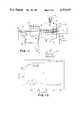
- FIG. 1is a schematic of a microwave plasma nitridation reactor especially useful in carrying out the process of the present invention
- FIG. 2is a grazing angle RBS spectra (random in line for plasma nitride sample VII);
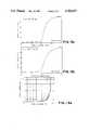
- FIG. 3shows high frequency (1 MHz) C-V characteristics of MIS devices with gate area of 7.85 ⁇ 10 -5 cm 2 (a) plasma nitride VII, (b) plasma nitride X;
- FIG. 1shows the plasma nitridation system utilized in the present invention.
- a waveguideis used to transfer microwave power from a 2.45 GHz microwave generator 12 through a 3-port. circulator (not shown) to the resonant cavity 10.
- the amount of microwave power transferred to the resonant cavity of the quartz tube 16can be adjusted from zero to more than 3 kW.
- Nitrogen gas to define the atmosphere within the quartz tubeis provided through a tube 18 to one end 20 of the quartz tube; this gas flows through the quartz tube to the resonant microwave cavity. Nitrogen plasma is generated inside the quartz tube by microwave discharge.
- the quartz tube 16guides the nitrogen plasma from the cavity into the nitridation ambient 22 and to the surface of the silicon wafer 24.
- the resonant cavityis tuned by conductive pins indicated generally at 26 to enable the plasma to extend to the surface of the silicon wafer and maximize its intensity for a fixed incident microwave power.
- a doped silicon rod 28is provided at the same end of the quartz tube as the gas inlet; the silicon rod 28 functions as an anodization electrode. It is electrically connected to a dc power supply 30 whose voltage can vary from zero to 1000 volts.
- the nitridation chamber itself 32is made of stainless steel and has four ports.
- One port 34is connected to a pumping system 36.
- Another port 38has the sample holder for wafer 24 which consists of a heater 40 and a thermocouple.
- the heaters 40were powered by a temperature controller 42 to establish a constant substrate temperature during each experiment.
- a further port 44 provided at the top of the chamber 32was provided for plasma-intensity monitoring using a phototransistor.
- the pumpingwas done by a constant speed mechanical pump without the use of an optional diffusion pump.
- the nitrogen pressurewas controlled by adjusting the flow rate of the gas.
- a photosensor 46was used at the chamber port 44 for plasma intensity measurement.
- the silicon wafer 24 mounted on a quartz insulator,was connected to a small dc voltage source 50. This wafer functions as the second electrode of the anodization circuit by making electrical connections to its edge.
- the waferwas electrically isolated from the heating block and the system ground comprising the stainless steel chamber and the cavity resonator.
- This configurationallows the application of a small dc voltage (usually less than or equal to 50 volts) to the silicon wafer (in addition to the power supply connected to the doped silicon rod) to make the plasma currents at the wafer and at the silicon rod equal. Unless these two currents are equal, it is found that there will be undesirable interaction between nitrogen plasma and the stainless steel chamber because of lack of enough plasma confinement causing possible contamination problems. Under the typical experimental growth conditions, the plasma electrical currents measured at the wafer 24 and at the silicon rod 28 locations are equal regardless of the exact value of the dc voltage applied to the silicon wafer 24. Therefore, in order to achieve equal currents it is not necessary to adjust the wafer dc bias 50 at a finely predetermined voltage value.
- the plasma stream 22may spread out of the quartz confinement parts 52. This problem will then disturb the equality balance between the two plasma currents.
- the equality balancecan be restored by gradually increasing the wafer bias voltage 50 and monitoring the two current meters 54, 56 until their readings become equal again. If the wafer bias voltage 50 is raised beyond this minimum required value, the two plasma current levels will still remain the same and the plasma confinement condition for minimizing any contamination risk will be satisfied. Under the normal nitridation conditions, the nitrogen plasma is confined locally around the silicon wafer by quartz confinement parts 52.
- positive anodization currentcorresponds to positively biased silicon wafer (negative voltage on the doped silicon rod).
- NHnegative voltage on the doped silicon rod.
- All the runs except for VI and Xwere performed with anodization current and silicon wafer biased positively with respect to the silicon rod. In run VI no anodization was used and in run X the silicon was biased negatively with respect to the silicon rod.
- the plasma currentif present, consists of two components. These components are the electronic and ionic currents. Considering the much higher mobility of electrons, the plasma current is expected to be dominated by the electronic current component.
- the systemwas pumped down after loading the silicon wafer in the nitridation chamber. Then the desired nitrogen pressure was established in the nitridation chamber by adjusting the nitrogen flow. Following heating the silicon wafer to be desired growth temperature, microwave nitrogen discharge was started by turning on the microwave power. Then the nitridation run was performed with or without anodization current. The films were then studied by optical and scanning electron microscopy, ellipsometry and grazing angle (83°) RBS. Moreover, metal-insulator-semiconductor devices were fabricated for electrical characterization purposes.
- FIG. 2illustrates the RBS grazing angle and random spectra for the plasma nitride sample VII.
- the aligned spectrumindicates the presence of C, N, O, and Si in the film.
- the high channel number peakindicated the presence of small amount of a heavy metal in the film.
- ESCAXPS
- the heavy metal contaminationis actually due to Pt. It is possible that the Pt contamination comes from the Pt wire which makes the electrical connection to the doped silicon rod in the plasma reactor.
- the quantitative calculations shown that the areal concentration of Ptis several orders of magnitude less than the areal concentrations of N or Si. For instance, the areal density of Pt in the plasma nitride sample VII was found to be 4.73 ⁇ 10 13 atoms/cm 2 .
- the absolute areal concentrations of the elementswere calculated from the areas of various elemental peaks in the aligned RBS spectrum.
- Table 2illustrates the ellipsometry thickness and the concentration data for plasma nitrided samples of various nitridation runs.
- the areal silicon concentration datahave been corrected for the substrate contribution to the silicon signal.
- the substrate contribution to the silicon signalwas estimated to be about 2.64 ⁇ 10 16 atoms/cm 2 for 2.2 MeV incident He+ particles.
- the fractional nitrogen concentration([N]/[N]+[O]+[C]) varies from 0.18 for run I to 0.48 for run IV. For all the samples except for I, IX, and X, this ratio is equal to or more than 0.40. It is expected that the dominant source of the oxygen contamination in the films is the original native oxide present on the surface of silicon prior to nitridation. The most possible explanation for carbon contamination is given based on the oil backstreaming from the mechanical pump. In order to reduce the undesirable contamination in the films, we have recently employed a diffusion pump (backed up a mechanical pump) equipped with a liquid nitrogen trap to maintain the low pressure in the nitridation chamber. This technique is expected to reduce the undesirable contamination significantly.
- FIGS. 3, 4, and 5illustrate the high frequency C-V, electrical breakdown, and the I-V characteristics of the devices with the plasma nitride films VII and X.
- Table 3shows the summary of electrical characterization data obtained from MIS devices fabricated with various plasma nitride insulators.
- the breakdown field for the plasma nitride VIIwas 8.9 MV/cm which is more than that (7.3 MV/cm) for V.
- the effect of substrate heatingwas to improve the electrical characteristics and the thickness uniformity across the wafer.
- the lowest E BD (3.5 MV/cm)was obtained for sample VIII which was the thickest sample grown with 140 mA of anodization current. Therefore, very large anodization current may degrade the quality of the grown insulator.
- the best breakdown distributionwas for sample X which was grown with reverse anodization current (wafer:-, Si rod:+).
- the flatband and threshold voltage data in Table 3were obtained from the C-V characteristics of various samples.
- the data in Table 3indicate that the flatband voltage shifted to more positive values when no substrate heating was employed, or a very large anodization current was present during the run.
- the positive shift of the flatband voltagecan be explained in terms of negative charge or electron trapping in the insulator. It seems that the electrons in the plasma current are trapped more easily in the insulator when the substrate temperature is low (no heating). Moreover, very large anodization current results in measurable negative charge trapping (even when substrate is heated) due to the large current density flowing through the film during the growth.
- the I-V dataindicated that the conduction is most possibly due to the Fowler-Nordheim injection of charge carriers. More data will be presented on time dependent breakdown, charge tapping, and oxidation resistance characteristics.
- the present inventioncomprises a microwave discharge technique which is successful in performing direct nitridation of silicon at relatively low, i.e., no more than about 500° C. growth temperatures in nitrogen plasma ambient without the presence of hydrogen or fluorine containing species.
- the as-grown filmshow good electrical characteristics. Modifications of the present invention may become apparent to a person of skill in the art who studies this disclosure. Therefore, this invention is to be limited only by the following claims.
Landscapes
- Chemical & Material Sciences (AREA)
- Chemical Kinetics & Catalysis (AREA)
- Engineering & Computer Science (AREA)
- Materials Engineering (AREA)
- Mechanical Engineering (AREA)
- Metallurgy (AREA)
- Organic Chemistry (AREA)
- Formation Of Insulating Films (AREA)
Abstract
Description
This invention was made with U.S. Government support under Army Agreement No. MDA903-84-K-0062, awarded by DARPA. The Government has certain rights in this invention.
This application is directed generally to the field of thin films for integrated circuits, and more particularly to the formation of silicon nitride films for use as ultra-thin gate, tunnel, and DRAM insulators in VLSI devices.
Due to the continuing increase in integration density of integrated circuits, and the reduction in device and circuit geometries, ultra-thin (less than or equal to 200 angstroms), high quality insulators are needed for gate insulators of IGFETs, storage capacitor insulators of DRAMs, and tunnel dielectrics in nonvolatile memories. Thermal nitrides and nitroxides prepared by direct thermal reaction of ammonia or nitrogen-containing species with silicon and silicon dioxide are of the best alternatives to thermally grown silicon dioxide for these particular applications. A number of techniques have been used previously for growth of thermal nitrides and nitroxides. These techniques include nonplasma thermal nitridation in ammonia or nitrogen ambient, rapid thermal nitridation in lamp-heated systems, high pressure nitridation, RF plasma-enhanced nitridation, and laser-enhanced nitridation. The techniques are generally summarized and reviewed in "Thermal Nitridation of Si and SiO2 for VLSI", Moslehi and Saraswat, IEEE Transactions on Electron Devices, February 1985. The conventional thermal nitridation process needs fairly high temperatures to grow relatively thick silicon nitride films, and usually the thickness is limited to about 70 angstroms at the highest growth temperature.
It is an object of the present invention to define an improved process for forming nitride films on silicon for use as ultra-thin insulators.
More particularly, it is an objective of the present invention to define a process capable of growing nitride films of thicknesses up to at least 100 angstroms.
In the basic techniques typically used to date, fairly high temperatures must be used. Unfortunately, as the geometry of integrated circuits continues to shrink, the use of high temperature processing in forming nitride insulators can cause migration of the impurities used to define the physical structure of the integrated circuit device. This can have a negative impact on the performance of the finished device. Therefore, it is an objective of this invention to define a process for providing nitride films which operates at relatively low temperatures. Preferably, the process to be defined would operate without any heating of the wafer, or with heating of the wafer to about 500.
In previous works on plasma-enhanced nitridation, the plasma was normally generated by RF discharge using electrodes or coils. However, in such techniques, the growth temperatures usually exceeded 900° C. and the film thicknesses were limited to small values. Reisman, et al., in "Nitridation of Silicon in a Multi-Wafer Plasma System," Journal Electronic Materials, Vol. 13, No. 3, 1984, describes nitridation of silicon in a multi-wafer RF (400 kHz) plasma system in an Ar-NH3 plasma mixture at less than or equal to 850° C., and grew very thin layers (up to 70 angstroms) of nitride films. Hezel, et al., "Silicon Oxynitride Films Prepared by Plasma Nitridation of Silicon and Their Application for Tunnel Metal-Insulator-Semiconductor Diodes," Journal Applied Physics, Vol. 56, No. 6, page 1756, 1984, used aparallel plate 30 kHz plasma reactor and a mixture of H2 --NH3 plasma to nitridize Si at 340° C. Using this approach, they could grow up to 60 angstrom nitride films. Using a laser-enhanced technique, Sugii, et al., "Excimer Laser Enhanced Nitridation of Silicon Substrates," Applied Physics Letters, Vol. 45 (9), page 966, 1984, were able to grow less than or equal to 25 angstroms of nitride at a substrate temperature of 400° C. The enhancement of the nitridation was attributed to the photochemically generated NH2 radicals by 6.4 eV laser photons. Harayama, et al., "Plasma Anodic Nitridation of Silicon in N2 --H2 System," Journal Electrochemical Society, Volume 131, No. 3, 1984, used a plasma anodic nitridation technique to form nitride films of up to 200 angstroms thick in N2 --H2 plasma system (13.56 MHz). Comparison of various nitridation techniques described above indicates that hydrogen was present in the plasma ambient in these projects; however, they do not present data regarding the amount of hydrogen incorporated into the composition of the grown films. Nakamura, et al., "Thermal Nitridation of Silicon and Nitrogen Plasma," Applied Physics Letters, Vol. 43(7), page 691, 1983, reported their results on thermal nitridation of silicon in nitrogen plasma (400 kHz). Under extreme nitridation conditions (1145° C., 10 hours), they could grow only 40 angstroms. Recently, Giridhar, et al., "SF6 Enhanced Nitridation of Silicon in Active Nitrogen," Applied Physics Letters, Vol. 45 (5), page 578, 1984 performed thermal nitridation of silicon and active nitrogen generated by microwave discharge and grew about 20 angstroms at 1100° C. for 60 minutes of nitridation in pure nitrogen plasma. The growth kinetics were significantly increased by addition of SF6 to the nitrogen ambient.
However, a difficulty with the techniques described in the references cited above is that the films are of insufficient thickness; they are formed at high temperatures; and they incorporate fluorine and/or hydrogen in the atmosphere present. The presence of these elements in the atmosphere can result in sputtering on the silicon surface resulting in deposited rather than grown films. Therefore, it is an objective of the present invention to define a process for growing thin nitride films of up to 100 angstroms thickness without incorporating fluorine or hydrogen in the nitride atmosphere.
Another objective of this invention is to grow these films at temperatures of 500° C. or less.
In brief, the present invention incorporates a process comprising direct plasma nitridation of silicon performed at low temperatures (500° C. or less) utilizing nitrogen plasma generated by microwave discharge. In a preferred embodiment, electrical connections are provided to the wafer in the plasma chamber and a silicon rod inserted in another region of the chamber to equalize the plasma currents at the wafer and minimize contamination of the film. Preferably, the anodization current is maintained at a low level, and comprises a reverse anodization current (wafer:-, Si rod:+) of a relatively small value. The microwave discharge is preferably about 2.45 GHz. The features and advantages of the present invention will be described with reference to the following figures, wherein
FIG. 1 is a schematic of a microwave plasma nitridation reactor especially useful in carrying out the process of the present invention;
FIG. 2 is a grazing angle RBS spectra (random in line for plasma nitride sample VII);
FIG. 3 shows high frequency (1 MHz) C-V characteristics of MIS devices with gate area of 7.85×10⁻⁵ cm2 (a) plasma nitride VII, (b) plasma nitride X;
FIG. 4 is a graph of electrical breakdown characteristics for MIS devices fabricated with plasma nitride insulators (area=7.85×10⁻⁵ cm2): (a) plasma nitride VII; (b) plasma nitride X. The results of measurements on several devices on each wafer are shown.
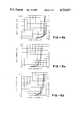
FIG. 5 shows I-V characteristics of MIS devices with (a) 47 angstrom (plasma nitride VII); and (b) 40 angstrom (plasma nitride X) plasma nitride insulators (area=7.85×10⁻⁵ cm2); several measurement results are shown in each case.
FIG. 1 shows the plasma nitridation system utilized in the present invention. A waveguide is used to transfer microwave power from a 2.45GHz microwave generator 12 through a 3-port. circulator (not shown) to theresonant cavity 10. The amount of microwave power transferred to the resonant cavity of thequartz tube 16 can be adjusted from zero to more than 3 kW. Nitrogen gas to define the atmosphere within the quartz tube is provided through atube 18 to oneend 20 of the quartz tube; this gas flows through the quartz tube to the resonant microwave cavity. Nitrogen plasma is generated inside the quartz tube by microwave discharge. Thequartz tube 16 guides the nitrogen plasma from the cavity into thenitridation ambient 22 and to the surface of thesilicon wafer 24. The resonant cavity is tuned by conductive pins indicated generally at 26 to enable the plasma to extend to the surface of the silicon wafer and maximize its intensity for a fixed incident microwave power. A dopedsilicon rod 28 is provided at the same end of the quartz tube as the gas inlet; thesilicon rod 28 functions as an anodization electrode. It is electrically connected to adc power supply 30 whose voltage can vary from zero to 1000 volts.
The nitridation chamber itself 32 is made of stainless steel and has four ports. Oneport 34 is connected to apumping system 36. Anotherport 38 has the sample holder forwafer 24 which consists of aheater 40 and a thermocouple. Theheaters 40 were powered by atemperature controller 42 to establish a constant substrate temperature during each experiment. Afurther port 44 provided at the top of thechamber 32 was provided for plasma-intensity monitoring using a phototransistor.
In the experiments described below, the pumping was done by a constant speed mechanical pump without the use of an optional diffusion pump. The nitrogen pressure was controlled by adjusting the flow rate of the gas. Aphotosensor 46 was used at thechamber port 44 for plasma intensity measurement. The silicon wafer 24 mounted on a quartz insulator, was connected to a smalldc voltage source 50. This wafer functions as the second electrode of the anodization circuit by making electrical connections to its edge. The wafer was electrically isolated from the heating block and the system ground comprising the stainless steel chamber and the cavity resonator. This configuration allows the application of a small dc voltage (usually less than or equal to 50 volts) to the silicon wafer (in addition to the power supply connected to the doped silicon rod) to make the plasma currents at the wafer and at the silicon rod equal. Unless these two currents are equal, it is found that there will be undesirable interaction between nitrogen plasma and the stainless steel chamber because of lack of enough plasma confinement causing possible contamination problems. Under the typical experimental growth conditions, the plasma electrical currents measured at thewafer 24 and at thesilicon rod 28 locations are equal regardless of the exact value of the dc voltage applied to thesilicon wafer 24. Therefore, in order to achieve equal currents it is not necessary to adjust thewafer dc bias 50 at a finely predetermined voltage value. However, under some unusual experimental conditions (e.g., very high microwave power in excess of 1.2 kW) theplasma stream 22 may spread out of thequartz confinement parts 52. This problem will then disturb the equality balance between the two plasma currents. The equality balance can be restored by gradually increasing thewafer bias voltage 50 and monitoring the twocurrent meters wafer bias voltage 50 is raised beyond this minimum required value, the two plasma current levels will still remain the same and the plasma confinement condition for minimizing any contamination risk will be satisfied. Under the normal nitridation conditions, the nitrogen plasma is confined locally around the silicon wafer byquartz confinement parts 52.
In all the nitridation experiments, 2-inch n-type <100> Si wafers with resistivities in the range of 0.1 to 0.9 ohm-cm were used. The experimental conditions for ten runs are shown in Table 1. In this table, Pi, Pr, I, T, t, and P, are the incident microwave power, reflected microwave power, anodization or plasma current, substrate temperature, nitridation time, and nitrogen gas pressure in the nitridation chamber, respectively. In each experiment the reflected microwave power was minimized by tuning the waveguide stubs 14 and cavity tuning pins. In all the experiments the nitrogen gas flow was adjusted to product the desired gas pressure under constant speed pumping by a mechanical pump. The doped silicon rod voltage determined the amount of anodization current in each experiment.
By definition, positive anodization current corresponds to positively biased silicon wafer (negative voltage on the doped silicon rod). The last four runs were performed at 500° C. substrate temperature whereas in the other runs (NH) the heater was off and the wafer temperature rise due to the excited plasma species was estimated to be equal to or less than 300° C. All the runs except for VI and X were performed with anodization current and silicon wafer biased positively with respect to the silicon rod. In run VI no anodization was used and in run X the silicon was biased negatively with respect to the silicon rod.
The plasma current, if present, consists of two components. These components are the electronic and ionic currents. Considering the much higher mobility of electrons, the plasma current is expected to be dominated by the electronic current component. In each nitridation experiment, the system was pumped down after loading the silicon wafer in the nitridation chamber. Then the desired nitrogen pressure was established in the nitridation chamber by adjusting the nitrogen flow. Following heating the silicon wafer to be desired growth temperature, microwave nitrogen discharge was started by turning on the microwave power. Then the nitridation run was performed with or without anodization current. The films were then studied by optical and scanning electron microscopy, ellipsometry and grazing angle (83°) RBS. Moreover, metal-insulator-semiconductor devices were fabricated for electrical characterization purposes.
FIG. 2 illustrates the RBS grazing angle and random spectra for the plasma nitride sample VII. The aligned spectrum indicates the presence of C, N, O, and Si in the film. Moreover, the high channel number peak indicated the presence of small amount of a heavy metal in the film. Using ESCA (XPS) it was found that the heavy metal contamination is actually due to Pt. It is possible that the Pt contamination comes from the Pt wire which makes the electrical connection to the doped silicon rod in the plasma reactor. The quantitative calculations shown that the areal concentration of Pt is several orders of magnitude less than the areal concentrations of N or Si. For instance, the areal density of Pt in the plasma nitride sample VII was found to be 4.73×10¹³ atoms/cm2.
The absolute areal concentrations of the elements (C, N, O, Si) were calculated from the areas of various elemental peaks in the aligned RBS spectrum. Table 2 illustrates the ellipsometry thickness and the concentration data for plasma nitrided samples of various nitridation runs. In this table, the areal silicon concentration data have been corrected for the substrate contribution to the silicon signal. Using a freshly etched clean silicon sample as RBS standard, the substrate contribution to the silicon signal was estimated to be about 2.64×10¹⁶ atoms/cm2 for 2.2 MeV incident He+ particles.
According to Table 2, the fractional nitrogen concentration ([N]/[N]+[O]+[C]) varies from 0.18 for run I to 0.48 for run IV. For all the samples except for I, IX, and X, this ratio is equal to or more than 0.40. It is expected that the dominant source of the oxygen contamination in the films is the original native oxide present on the surface of silicon prior to nitridation. The most possible explanation for carbon contamination is given based on the oil backstreaming from the mechanical pump. In order to reduce the undesirable contamination in the films, we have recently employed a diffusion pump (backed up a mechanical pump) equipped with a liquid nitrogen trap to maintain the low pressure in the nitridation chamber. This technique is expected to reduce the undesirable contamination significantly. However, all the data presented in this paper are for the samples grown in the original system pumped only with the mechanical pump. The thickness (measured with Nf =2.0) varied from about 30 to 100 angstroms depending on the nitridation conditions. It was concluded that the growth kinetics was almost independent of temperature. This could be observed from runs V and VII which were performed under identical growth conditions except for substrate heating used in run VII. The thicknesses in both cases are nearly the same (51 angstroms and 47 angstroms) which indicates that the growth kinetics is almost independent of temperature.
The metal-insulator-semiconductor devices were tested for electrical characterization of the plasma nitride insulators. FIGS. 3, 4, and 5 illustrate the high frequency C-V, electrical breakdown, and the I-V characteristics of the devices with the plasma nitride films VII and X.
Table 3 shows the summary of electrical characterization data obtained from MIS devices fabricated with various plasma nitride insulators. As shown in this table, the breakdown field for the plasma nitride VII was 8.9 MV/cm which is more than that (7.3 MV/cm) for V. The effect of substrate heating was to improve the electrical characteristics and the thickness uniformity across the wafer. The lowest EBD (3.5 MV/cm) was obtained for sample VIII which was the thickest sample grown with 140 mA of anodization current. Therefore, very large anodization current may degrade the quality of the grown insulator. The best breakdown distribution was for sample X which was grown with reverse anodization current (wafer:-, Si rod:+). The flatband and threshold voltage data in Table 3 were obtained from the C-V characteristics of various samples. The data in Table 3 indicate that the flatband voltage shifted to more positive values when no substrate heating was employed, or a very large anodization current was present during the run. The positive shift of the flatband voltage can be explained in terms of negative charge or electron trapping in the insulator. It seems that the electrons in the plasma current are trapped more easily in the insulator when the substrate temperature is low (no heating). Moreover, very large anodization current results in measurable negative charge trapping (even when substrate is heated) due to the large current density flowing through the film during the growth.
The I-V data indicated that the conduction is most possibly due to the Fowler-Nordheim injection of charge carriers. More data will be presented on time dependent breakdown, charge tapping, and oxidation resistance characteristics.
Thus, the present invention comprises a microwave discharge technique which is successful in performing direct nitridation of silicon at relatively low, i.e., no more than about 500° C. growth temperatures in nitrogen plasma ambient without the presence of hydrogen or fluorine containing species. The as-grown film show good electrical characteristics. Modifications of the present invention may become apparent to a person of skill in the art who studies this disclosure. Therefore, this invention is to be limited only by the following claims.
TABLE 1 ______________________________________ PLASMA NITRIDATION EXPERIMENTS Run P.sub.i (KW) P.sub.r (W) I (mA) T (°C.) t (min) P (mtorrs) ______________________________________ I 0.8 80 10 NH 45 50 II 1.2 60 30NH 30 45 III 1.2 40 50 NH 80 65 IV 1.0 45 3.5 NH 180 73 V 1.0 45 44 NH 80 66 VI 1.0 45 00 NH 80 58 VII 1.0 45 44 500 80 70 VIII 1.2 50 140 500 80 63 IX 1.2 25 79 500 80 251 X 1.2 38 60 500 80 68 ______________________________________
TABLE II ______________________________________ THE ELLIPSOMETRY AND RBS DATA Run t.sub.N (Å) [C] (cm.sup.-2) [N] (cm.sup.-2) [O] (cm.sup.-2) [Si] (cm.sup.-2) ______________________________________ I 33 2.9 × 10.sup.16 1.0 × 10.sup.16 1.75 × 10.sup.16 1.84 × 10.sup.16 II 66 1.67 × 10.sup.16 2.55 × 10.sup.16 1.70 × 10.sup.16 2.60 × 10.sup.16 III 63 1.86 × 10.sup.16 3.49 × 10.sup.16 2.62 × 10.sup.16 3.58 × 10.sup.16 IV 56 1.73 × 10.sup.16 3.96 × 10.sup.16 2.54 × 10.sup.16 4.14 × 10.sup.16 V 51 1.55 × 10.sup.16 1.72 × 10.sup.16 1.06 × 10.sup.16 0.26 × 10.sup.16 VI 41 1.57 × 10.sup.16 2.16 × 10.sup.16 1.61 × 10.sup.16 2.31 × 10.sup.16 VII 47 1.60 × 10.sup.16 2.69 × 10.sup.16 1.84 × 10.sup.16 2.94 × 10.sup.16 VIII 100 3.61 × 10.sup.16 5.31 × 10.sup.16 2.95 × 10.sup.16 4.80 × 10.sup.16 IX 39 1.28 × 10.sup.16 7.63 × 10.sup.16 1.76 × 10.sup.16 0.38 × 10.sup.16 X 40 1.96 × 10.sup.16 1.76 × 10.sup.16 1.78 × 10.sup.16 1.91 × 10.sup.16 ______________________________________
TABLE III ______________________________________ THE ELECTRICAL CHARACTERIZATION RESULTS Run V.sub.FB (V) V.sub.TH (V) V.sub.BD (V) E.sub.BD (MV/cm) ______________________________________ III 1.53 0.82 3.7 5.9 IV 2.08 1.42 4.3 7.7 V 0.60 0.11 3.7 7.3 VII 0.16 0.54 4.2 8.9 VIII 0.71 0.04 3.5 3.5 IX 0.20 0.54 3.5 9.0 X 0.08 0.67 4.3 10.8 ______________________________________
Claims (7)
1. A low-temperature process for forming an ultra-thin silicon nitride film on a silicon substrate by direct plasma nitridation of silicon comprising the steps of
supporting a wafer comprising said silicon substrate on a wafer support in a stainless steel nitridation chamber,
leading a quartz tube from a nitrogen gas source into said plasma nitridation chamber through a resonant cavity,
establishing a fluorine and hydrogen-free nitrogen atmosphere in said quartz tube,
generating nitrogen plasma inside the resonant cavity of said quartz tube, said plasma extending through the quartz tube into said nitridation chamber to the surface of said wafer,
inserting a silicon rod into an end of said quartz tube distant from said wafer support, and
providing an electrical connection between said silicon rod and a first voltage source to produce an anodization current and an electrical connection between said wafer and a second voltage source to equalize the plasma currents at the wafer and the silicon rod to minimize contamination of said silicon nitride film.
2. A process as in claim 1 wherein the temperature of the wafer is 500° C. or less.
3. A process as in claim 1 wherein the wafer is heated to about 500° C. to improve the thickness uniformity of the wafer film.
4. A process as in claim 3 wherein said atmosphere consists of nitrogen.
5. A process as in claim 4 wherein the nitrogen plasma is generated by a microwave discharge at about 2.45 GHz.
6. A process as in claim 3 wherein the film is grown during application of reverse anodization current to said rod and said wafer.
7. A process as in claim 6 wherein the anodization current is maintained at a relatively low level.
Priority Applications (1)
| Application Number | Priority Date | Filing Date | Title |
|---|---|---|---|
| US06/859,943US4715937A (en) | 1986-05-05 | 1986-05-05 | Low-temperature direct nitridation of silicon in nitrogen plasma generated by microwave discharge |
Applications Claiming Priority (1)
| Application Number | Priority Date | Filing Date | Title |
|---|---|---|---|
| US06/859,943US4715937A (en) | 1986-05-05 | 1986-05-05 | Low-temperature direct nitridation of silicon in nitrogen plasma generated by microwave discharge |
Publications (1)
| Publication Number | Publication Date |
|---|---|
| US4715937Atrue US4715937A (en) | 1987-12-29 |
Family
ID=25332132
Family Applications (1)
| Application Number | Title | Priority Date | Filing Date |
|---|---|---|---|
| US06/859,943Expired - Fee RelatedUS4715937A (en) | 1986-05-05 | 1986-05-05 | Low-temperature direct nitridation of silicon in nitrogen plasma generated by microwave discharge |
Country Status (1)
| Country | Link |
|---|---|
| US (1) | US4715937A (en) |
Cited By (182)
| Publication number | Priority date | Publication date | Assignee | Title |
|---|---|---|---|---|
| US4902870A (en)* | 1989-03-31 | 1990-02-20 | General Electric Company | Apparatus and method for transfer arc cleaning of a substrate in an RF plasma system |
| US5023056A (en)* | 1989-12-27 | 1991-06-11 | The United States Of America As Represented By The Secretary Of The Navy | Plasma generator utilizing dielectric member for carrying microwave energy |
| US5041303A (en)* | 1988-03-07 | 1991-08-20 | Polyplasma Incorporated | Process for modifying large polymeric surfaces |
| US5264396A (en)* | 1993-01-14 | 1993-11-23 | Micron Semiconductor, Inc. | Method for enhancing nitridation and oxidation growth by introducing pulsed NF3 |
| US5510088A (en)* | 1992-06-11 | 1996-04-23 | The United States Of America As Represented By The Secretary Of The Navy | Low temperature plasma film deposition using dielectric chamber as source material |
| US5565248A (en)* | 1994-02-09 | 1996-10-15 | The Coca-Cola Company | Method and apparatus for coating hollow containers through plasma-assisted deposition of an inorganic substance |
| US5601883A (en)* | 1987-02-10 | 1997-02-11 | Semicondoctor Energy Laboratory Co., Inc. | Microwave enhanced CVD method for coating plastic with carbon films |
| US5849366A (en)* | 1994-02-16 | 1998-12-15 | The Coca-Cola Company | Hollow containers with inert or impermeable inner surface through plasma-assisted surface reaction or on-surface polymerization |
| US5906787A (en)* | 1994-02-18 | 1999-05-25 | The Coca-Cola Company | Hollow containers having a very thin inert or impermeable inner surface layer by coating the inside surface of the preform |
| US5913149A (en)* | 1992-12-31 | 1999-06-15 | Micron Technology, Inc. | Method for fabricating stacked layer silicon nitride for low leakage and high capacitance |
| US6077772A (en)* | 1998-05-11 | 2000-06-20 | Samsung Electronics Co., Ltd. | Methods of forming metal interconnections including thermally treated barrier layers |
| US6080665A (en)* | 1997-04-11 | 2000-06-27 | Applied Materials, Inc. | Integrated nitrogen-treated titanium layer to prevent interaction of titanium and aluminum |
| US6100188A (en)* | 1998-07-01 | 2000-08-08 | Texas Instruments Incorporated | Stable and low resistance metal/barrier/silicon stack structure and related process for manufacturing |
| US6143377A (en)* | 1994-12-26 | 2000-11-07 | Sony Corporation | Process of forming a refractory metal thin film |
| US6149982A (en)* | 1994-02-16 | 2000-11-21 | The Coca-Cola Company | Method of forming a coating on an inner surface |
| US6274510B1 (en) | 1998-07-15 | 2001-08-14 | Texas Instruments Incorporated | Lower temperature method for forming high quality silicon-nitrogen dielectrics |
| US6331468B1 (en)* | 1998-05-11 | 2001-12-18 | Lsi Logic Corporation | Formation of integrated circuit structure using one or more silicon layers for implantation and out-diffusion in formation of defect-free source/drain regions and also for subsequent formation of silicon nitride spacers |
| US6759315B1 (en)* | 1999-01-04 | 2004-07-06 | International Business Machines Corporation | Method for selective trimming of gate structures and apparatus formed thereby |
| US20040224534A1 (en)* | 2002-12-18 | 2004-11-11 | Beulens Jacobus Johannes | Method of fabricating silicon nitride nanodots |
| US20040235311A1 (en)* | 2001-08-02 | 2004-11-25 | Toshio Nakanishi | Base method treating method and electron device-use material |
| US20040259341A1 (en)* | 2003-06-20 | 2004-12-23 | Taiwan Semicondutor Manufacturing Co. | Method of forming dual gate insulator layers for CMOS applications |
| US20050048705A1 (en)* | 2003-08-26 | 2005-03-03 | International Business Machines Corporation | Method for fabricating a nitrided silicon-oxide gate dielectric |
| US20050118837A1 (en)* | 2002-07-19 | 2005-06-02 | Todd Michael A. | Method to form ultra high quality silicon-containing compound layers |
| US20060084201A1 (en)* | 2004-10-15 | 2006-04-20 | Albert Hasper | Parts for deposition reactors |
| US20060105107A1 (en)* | 2004-10-15 | 2006-05-18 | Lindeboom Bartholomeus H L | Reactor design for reduced particulate generation |
| US20060199357A1 (en)* | 2005-03-07 | 2006-09-07 | Wan Yuet M | High stress nitride film and method for formation thereof |
| US20070054048A1 (en)* | 2005-09-07 | 2007-03-08 | Suvi Haukka | Extended deposition range by hot spots |
| US20070141851A1 (en)* | 2005-12-16 | 2007-06-21 | Selen Louis J | System and method of reducing particle contamination of semiconductor substrates |
| US20070166966A1 (en)* | 2004-09-03 | 2007-07-19 | Asm America, Inc. | Deposition from liquid sources |
| US20070254113A1 (en)* | 2000-03-24 | 2007-11-01 | Tokyo Electron Limited | Plasma processing apparatus having an evacuating arrangement to evacuate gas from gas-introducing part of a process chamber |
| US20090045447A1 (en)* | 2007-08-17 | 2009-02-19 | Micron Technology, Inc. | Complex oxide nanodots |
| US7629256B2 (en) | 2007-05-14 | 2009-12-08 | Asm International N.V. | In situ silicon and titanium nitride deposition |
| US7691757B2 (en) | 2006-06-22 | 2010-04-06 | Asm International N.V. | Deposition of complex nitride films |
| US7718518B2 (en) | 2005-12-16 | 2010-05-18 | Asm International N.V. | Low temperature doped silicon layer formation |
| US7732350B2 (en) | 2004-09-22 | 2010-06-08 | Asm International N.V. | Chemical vapor deposition of TiN films in a batch reactor |
| US7833906B2 (en) | 2008-12-11 | 2010-11-16 | Asm International N.V. | Titanium silicon nitride deposition |
| US8012876B2 (en) | 2008-12-02 | 2011-09-06 | Asm International N.V. | Delivery of vapor precursor from solid source |
| US20140099794A1 (en)* | 2012-09-21 | 2014-04-10 | Applied Materials, Inc. | Radical chemistry modulation and control using multiple flow pathways |
| US9117855B2 (en) | 2013-12-04 | 2015-08-25 | Applied Materials, Inc. | Polarity control for remote plasma |
| US9132436B2 (en) | 2012-09-21 | 2015-09-15 | Applied Materials, Inc. | Chemical control features in wafer process equipment |
| US9136273B1 (en) | 2014-03-21 | 2015-09-15 | Applied Materials, Inc. | Flash gate air gap |
| US9153442B2 (en) | 2013-03-15 | 2015-10-06 | Applied Materials, Inc. | Processing systems and methods for halide scavenging |
| US9159606B1 (en) | 2014-07-31 | 2015-10-13 | Applied Materials, Inc. | Metal air gap |
| US9165786B1 (en) | 2014-08-05 | 2015-10-20 | Applied Materials, Inc. | Integrated oxide and nitride recess for better channel contact in 3D architectures |
| US9190293B2 (en) | 2013-12-18 | 2015-11-17 | Applied Materials, Inc. | Even tungsten etch for high aspect ratio trenches |
| US9209012B2 (en) | 2013-09-16 | 2015-12-08 | Applied Materials, Inc. | Selective etch of silicon nitride |
| US9236266B2 (en) | 2011-08-01 | 2016-01-12 | Applied Materials, Inc. | Dry-etch for silicon-and-carbon-containing films |
| US9236265B2 (en) | 2013-11-04 | 2016-01-12 | Applied Materials, Inc. | Silicon germanium processing |
| US9245762B2 (en) | 2013-12-02 | 2016-01-26 | Applied Materials, Inc. | Procedure for etch rate consistency |
| US9263278B2 (en) | 2013-12-17 | 2016-02-16 | Applied Materials, Inc. | Dopant etch selectivity control |
| US9269590B2 (en) | 2014-04-07 | 2016-02-23 | Applied Materials, Inc. | Spacer formation |
| US9287095B2 (en) | 2013-12-17 | 2016-03-15 | Applied Materials, Inc. | Semiconductor system assemblies and methods of operation |
| US9287134B2 (en) | 2014-01-17 | 2016-03-15 | Applied Materials, Inc. | Titanium oxide etch |
| US9293568B2 (en) | 2014-01-27 | 2016-03-22 | Applied Materials, Inc. | Method of fin patterning |
| US9299575B2 (en) | 2014-03-17 | 2016-03-29 | Applied Materials, Inc. | Gas-phase tungsten etch |
| US9299583B1 (en) | 2014-12-05 | 2016-03-29 | Applied Materials, Inc. | Aluminum oxide selective etch |
| US9299582B2 (en) | 2013-11-12 | 2016-03-29 | Applied Materials, Inc. | Selective etch for metal-containing materials |
| US9299538B2 (en) | 2014-03-20 | 2016-03-29 | Applied Materials, Inc. | Radial waveguide systems and methods for post-match control of microwaves |
| US9299537B2 (en) | 2014-03-20 | 2016-03-29 | Applied Materials, Inc. | Radial waveguide systems and methods for post-match control of microwaves |
| US9309598B2 (en) | 2014-05-28 | 2016-04-12 | Applied Materials, Inc. | Oxide and metal removal |
| US9324576B2 (en) | 2010-05-27 | 2016-04-26 | Applied Materials, Inc. | Selective etch for silicon films |
| US9343272B1 (en) | 2015-01-08 | 2016-05-17 | Applied Materials, Inc. | Self-aligned process |
| US9349605B1 (en) | 2015-08-07 | 2016-05-24 | Applied Materials, Inc. | Oxide etch selectivity systems and methods |
| US9355856B2 (en) | 2014-09-12 | 2016-05-31 | Applied Materials, Inc. | V trench dry etch |
| US9355862B2 (en) | 2014-09-24 | 2016-05-31 | Applied Materials, Inc. | Fluorine-based hardmask removal |
| US9355863B2 (en) | 2012-12-18 | 2016-05-31 | Applied Materials, Inc. | Non-local plasma oxide etch |
| US9362130B2 (en) | 2013-03-01 | 2016-06-07 | Applied Materials, Inc. | Enhanced etching processes using remote plasma sources |
| US9368364B2 (en) | 2014-09-24 | 2016-06-14 | Applied Materials, Inc. | Silicon etch process with tunable selectivity to SiO2 and other materials |
| US9373522B1 (en) | 2015-01-22 | 2016-06-21 | Applied Mateials, Inc. | Titanium nitride removal |
| US9373517B2 (en) | 2012-08-02 | 2016-06-21 | Applied Materials, Inc. | Semiconductor processing with DC assisted RF power for improved control |
| US9378978B2 (en) | 2014-07-31 | 2016-06-28 | Applied Materials, Inc. | Integrated oxide recess and floating gate fin trimming |
| US9378969B2 (en) | 2014-06-19 | 2016-06-28 | Applied Materials, Inc. | Low temperature gas-phase carbon removal |
| US9385028B2 (en) | 2014-02-03 | 2016-07-05 | Applied Materials, Inc. | Air gap process |
| US9384997B2 (en) | 2012-11-20 | 2016-07-05 | Applied Materials, Inc. | Dry-etch selectivity |
| US9390937B2 (en) | 2012-09-20 | 2016-07-12 | Applied Materials, Inc. | Silicon-carbon-nitride selective etch |
| US9396989B2 (en) | 2014-01-27 | 2016-07-19 | Applied Materials, Inc. | Air gaps between copper lines |
| CN105807189A (en)* | 2014-12-29 | 2016-07-27 | 国家电网公司 | Test device and test method for local discharge development process of superconducting insulating material |
| US9406523B2 (en) | 2014-06-19 | 2016-08-02 | Applied Materials, Inc. | Highly selective doped oxide removal method |
| US9412608B2 (en) | 2012-11-30 | 2016-08-09 | Applied Materials, Inc. | Dry-etch for selective tungsten removal |
| US9418858B2 (en) | 2011-10-07 | 2016-08-16 | Applied Materials, Inc. | Selective etch of silicon by way of metastable hydrogen termination |
| US9425058B2 (en) | 2014-07-24 | 2016-08-23 | Applied Materials, Inc. | Simplified litho-etch-litho-etch process |
| US9437451B2 (en) | 2012-09-18 | 2016-09-06 | Applied Materials, Inc. | Radical-component oxide etch |
| US9449846B2 (en) | 2015-01-28 | 2016-09-20 | Applied Materials, Inc. | Vertical gate separation |
| US9449845B2 (en) | 2012-12-21 | 2016-09-20 | Applied Materials, Inc. | Selective titanium nitride etching |
| US9478432B2 (en) | 2014-09-25 | 2016-10-25 | Applied Materials, Inc. | Silicon oxide selective removal |
| US9496167B2 (en) | 2014-07-31 | 2016-11-15 | Applied Materials, Inc. | Integrated bit-line airgap formation and gate stack post clean |
| US9493879B2 (en) | 2013-07-12 | 2016-11-15 | Applied Materials, Inc. | Selective sputtering for pattern transfer |
| US9499898B2 (en) | 2014-03-03 | 2016-11-22 | Applied Materials, Inc. | Layered thin film heater and method of fabrication |
| US9502258B2 (en) | 2014-12-23 | 2016-11-22 | Applied Materials, Inc. | Anisotropic gap etch |
| US9553102B2 (en) | 2014-08-19 | 2017-01-24 | Applied Materials, Inc. | Tungsten separation |
| US9576809B2 (en) | 2013-11-04 | 2017-02-21 | Applied Materials, Inc. | Etch suppression with germanium |
| US9607856B2 (en) | 2013-03-05 | 2017-03-28 | Applied Materials, Inc. | Selective titanium nitride removal |
| US9659753B2 (en) | 2014-08-07 | 2017-05-23 | Applied Materials, Inc. | Grooved insulator to reduce leakage current |
| US9691645B2 (en) | 2015-08-06 | 2017-06-27 | Applied Materials, Inc. | Bolted wafer chuck thermal management systems and methods for wafer processing systems |
| US9721789B1 (en) | 2016-10-04 | 2017-08-01 | Applied Materials, Inc. | Saving ion-damaged spacers |
| US9728437B2 (en) | 2015-02-03 | 2017-08-08 | Applied Materials, Inc. | High temperature chuck for plasma processing systems |
| US9741593B2 (en) | 2015-08-06 | 2017-08-22 | Applied Materials, Inc. | Thermal management systems and methods for wafer processing systems |
| US9768034B1 (en) | 2016-11-11 | 2017-09-19 | Applied Materials, Inc. | Removal methods for high aspect ratio structures |
| US9773648B2 (en) | 2013-08-30 | 2017-09-26 | Applied Materials, Inc. | Dual discharge modes operation for remote plasma |
| US9842744B2 (en) | 2011-03-14 | 2017-12-12 | Applied Materials, Inc. | Methods for etch of SiN films |
| US9847289B2 (en) | 2014-05-30 | 2017-12-19 | Applied Materials, Inc. | Protective via cap for improved interconnect performance |
| US9865484B1 (en) | 2016-06-29 | 2018-01-09 | Applied Materials, Inc. | Selective etch using material modification and RF pulsing |
| US9881805B2 (en) | 2015-03-02 | 2018-01-30 | Applied Materials, Inc. | Silicon selective removal |
| US9885117B2 (en) | 2014-03-31 | 2018-02-06 | Applied Materials, Inc. | Conditioned semiconductor system parts |
| US9887096B2 (en) | 2012-09-17 | 2018-02-06 | Applied Materials, Inc. | Differential silicon oxide etch |
| US9934942B1 (en) | 2016-10-04 | 2018-04-03 | Applied Materials, Inc. | Chamber with flow-through source |
| US9947549B1 (en) | 2016-10-10 | 2018-04-17 | Applied Materials, Inc. | Cobalt-containing material removal |
| US10026621B2 (en) | 2016-11-14 | 2018-07-17 | Applied Materials, Inc. | SiN spacer profile patterning |
| US10043684B1 (en) | 2017-02-06 | 2018-08-07 | Applied Materials, Inc. | Self-limiting atomic thermal etching systems and methods |
| US10043674B1 (en) | 2017-08-04 | 2018-08-07 | Applied Materials, Inc. | Germanium etching systems and methods |
| US10049891B1 (en) | 2017-05-31 | 2018-08-14 | Applied Materials, Inc. | Selective in situ cobalt residue removal |
| US10062587B2 (en) | 2012-07-18 | 2018-08-28 | Applied Materials, Inc. | Pedestal with multi-zone temperature control and multiple purge capabilities |
| US10062585B2 (en) | 2016-10-04 | 2018-08-28 | Applied Materials, Inc. | Oxygen compatible plasma source |
| US10062579B2 (en) | 2016-10-07 | 2018-08-28 | Applied Materials, Inc. | Selective SiN lateral recess |
| US10062578B2 (en) | 2011-03-14 | 2018-08-28 | Applied Materials, Inc. | Methods for etch of metal and metal-oxide films |
| US10062575B2 (en) | 2016-09-09 | 2018-08-28 | Applied Materials, Inc. | Poly directional etch by oxidation |
| US10128086B1 (en) | 2017-10-24 | 2018-11-13 | Applied Materials, Inc. | Silicon pretreatment for nitride removal |
| US10163696B2 (en) | 2016-11-11 | 2018-12-25 | Applied Materials, Inc. | Selective cobalt removal for bottom up gapfill |
| US10170282B2 (en) | 2013-03-08 | 2019-01-01 | Applied Materials, Inc. | Insulated semiconductor faceplate designs |
| US10170336B1 (en) | 2017-08-04 | 2019-01-01 | Applied Materials, Inc. | Methods for anisotropic control of selective silicon removal |
| US10224210B2 (en) | 2014-12-09 | 2019-03-05 | Applied Materials, Inc. | Plasma processing system with direct outlet toroidal plasma source |
| US10242908B2 (en) | 2016-11-14 | 2019-03-26 | Applied Materials, Inc. | Airgap formation with damage-free copper |
| US10256112B1 (en) | 2017-12-08 | 2019-04-09 | Applied Materials, Inc. | Selective tungsten removal |
| US10283321B2 (en) | 2011-01-18 | 2019-05-07 | Applied Materials, Inc. | Semiconductor processing system and methods using capacitively coupled plasma |
| US10283324B1 (en) | 2017-10-24 | 2019-05-07 | Applied Materials, Inc. | Oxygen treatment for nitride etching |
| US10297458B2 (en) | 2017-08-07 | 2019-05-21 | Applied Materials, Inc. | Process window widening using coated parts in plasma etch processes |
| US10319739B2 (en) | 2017-02-08 | 2019-06-11 | Applied Materials, Inc. | Accommodating imperfectly aligned memory holes |
| US10319600B1 (en) | 2018-03-12 | 2019-06-11 | Applied Materials, Inc. | Thermal silicon etch |
| US10319649B2 (en) | 2017-04-11 | 2019-06-11 | Applied Materials, Inc. | Optical emission spectroscopy (OES) for remote plasma monitoring |
| US10354889B2 (en) | 2017-07-17 | 2019-07-16 | Applied Materials, Inc. | Non-halogen etching of silicon-containing materials |
| US10403507B2 (en) | 2017-02-03 | 2019-09-03 | Applied Materials, Inc. | Shaped etch profile with oxidation |
| US10431429B2 (en) | 2017-02-03 | 2019-10-01 | Applied Materials, Inc. | Systems and methods for radial and azimuthal control of plasma uniformity |
| US10468267B2 (en) | 2017-05-31 | 2019-11-05 | Applied Materials, Inc. | Water-free etching methods |
| WO2019212938A1 (en)* | 2018-04-29 | 2019-11-07 | Applied Materials, Inc. | Low temperature atomic layer deposition of silicon nitride |
| US10490406B2 (en) | 2018-04-10 | 2019-11-26 | Appled Materials, Inc. | Systems and methods for material breakthrough |
| US10490418B2 (en) | 2014-10-14 | 2019-11-26 | Applied Materials, Inc. | Systems and methods for internal surface conditioning assessment in plasma processing equipment |
| US10497573B2 (en) | 2018-03-13 | 2019-12-03 | Applied Materials, Inc. | Selective atomic layer etching of semiconductor materials |
| US10504700B2 (en) | 2015-08-27 | 2019-12-10 | Applied Materials, Inc. | Plasma etching systems and methods with secondary plasma injection |
| US10504754B2 (en) | 2016-05-19 | 2019-12-10 | Applied Materials, Inc. | Systems and methods for improved semiconductor etching and component protection |
| US10522371B2 (en) | 2016-05-19 | 2019-12-31 | Applied Materials, Inc. | Systems and methods for improved semiconductor etching and component protection |
| US10541246B2 (en) | 2017-06-26 | 2020-01-21 | Applied Materials, Inc. | 3D flash memory cells which discourage cross-cell electrical tunneling |
| US10541184B2 (en) | 2017-07-11 | 2020-01-21 | Applied Materials, Inc. | Optical emission spectroscopic techniques for monitoring etching |
| US10546729B2 (en) | 2016-10-04 | 2020-01-28 | Applied Materials, Inc. | Dual-channel showerhead with improved profile |
| US10566206B2 (en) | 2016-12-27 | 2020-02-18 | Applied Materials, Inc. | Systems and methods for anisotropic material breakthrough |
| US10573496B2 (en) | 2014-12-09 | 2020-02-25 | Applied Materials, Inc. | Direct outlet toroidal plasma source |
| US10573527B2 (en) | 2018-04-06 | 2020-02-25 | Applied Materials, Inc. | Gas-phase selective etching systems and methods |
| US10593523B2 (en) | 2014-10-14 | 2020-03-17 | Applied Materials, Inc. | Systems and methods for internal surface conditioning in plasma processing equipment |
| US10593560B2 (en) | 2018-03-01 | 2020-03-17 | Applied Materials, Inc. | Magnetic induction plasma source for semiconductor processes and equipment |
| US10615047B2 (en) | 2018-02-28 | 2020-04-07 | Applied Materials, Inc. | Systems and methods to form airgaps |
| US10629473B2 (en) | 2016-09-09 | 2020-04-21 | Applied Materials, Inc. | Footing removal for nitride spacer |
| US10672642B2 (en) | 2018-07-24 | 2020-06-02 | Applied Materials, Inc. | Systems and methods for pedestal configuration |
| US10679870B2 (en) | 2018-02-15 | 2020-06-09 | Applied Materials, Inc. | Semiconductor processing chamber multistage mixing apparatus |
| US10699879B2 (en) | 2018-04-17 | 2020-06-30 | Applied Materials, Inc. | Two piece electrode assembly with gap for plasma control |
| US10727080B2 (en) | 2017-07-07 | 2020-07-28 | Applied Materials, Inc. | Tantalum-containing material removal |
| US10755941B2 (en) | 2018-07-06 | 2020-08-25 | Applied Materials, Inc. | Self-limiting selective etching systems and methods |
| US10854426B2 (en) | 2018-01-08 | 2020-12-01 | Applied Materials, Inc. | Metal recess for semiconductor structures |
| US10872778B2 (en) | 2018-07-06 | 2020-12-22 | Applied Materials, Inc. | Systems and methods utilizing solid-phase etchants |
| US10886137B2 (en) | 2018-04-30 | 2021-01-05 | Applied Materials, Inc. | Selective nitride removal |
| US10892198B2 (en) | 2018-09-14 | 2021-01-12 | Applied Materials, Inc. | Systems and methods for improved performance in semiconductor processing |
| US10903054B2 (en) | 2017-12-19 | 2021-01-26 | Applied Materials, Inc. | Multi-zone gas distribution systems and methods |
| US10920320B2 (en) | 2017-06-16 | 2021-02-16 | Applied Materials, Inc. | Plasma health determination in semiconductor substrate processing reactors |
| US10920319B2 (en) | 2019-01-11 | 2021-02-16 | Applied Materials, Inc. | Ceramic showerheads with conductive electrodes |
| WO2021030332A1 (en)* | 2019-08-13 | 2021-02-18 | Applied Materials, Inc. | Peald titanium nitride with direct microwave plasma |
| US10943834B2 (en) | 2017-03-13 | 2021-03-09 | Applied Materials, Inc. | Replacement contact process |
| US10950428B1 (en) | 2019-08-30 | 2021-03-16 | Mattson Technology, Inc. | Method for processing a workpiece |
| US10964512B2 (en) | 2018-02-15 | 2021-03-30 | Applied Materials, Inc. | Semiconductor processing chamber multistage mixing apparatus and methods |
| US11024486B2 (en) | 2013-02-08 | 2021-06-01 | Applied Materials, Inc. | Semiconductor processing systems having multiple plasma configurations |
| US11049755B2 (en) | 2018-09-14 | 2021-06-29 | Applied Materials, Inc. | Semiconductor substrate supports with embedded RF shield |
| US11062887B2 (en) | 2018-09-17 | 2021-07-13 | Applied Materials, Inc. | High temperature RF heater pedestals |
| US11121002B2 (en) | 2018-10-24 | 2021-09-14 | Applied Materials, Inc. | Systems and methods for etching metals and metal derivatives |
| US11239061B2 (en) | 2014-11-26 | 2022-02-01 | Applied Materials, Inc. | Methods and systems to enhance process uniformity |
| US11257693B2 (en) | 2015-01-09 | 2022-02-22 | Applied Materials, Inc. | Methods and systems to improve pedestal temperature control |
| US11276559B2 (en) | 2017-05-17 | 2022-03-15 | Applied Materials, Inc. | Semiconductor processing chamber for multiple precursor flow |
| US11276590B2 (en) | 2017-05-17 | 2022-03-15 | Applied Materials, Inc. | Multi-zone semiconductor substrate supports |
| US11328909B2 (en) | 2017-12-22 | 2022-05-10 | Applied Materials, Inc. | Chamber conditioning and removal processes |
| US11417534B2 (en) | 2018-09-21 | 2022-08-16 | Applied Materials, Inc. | Selective material removal |
| US11437242B2 (en) | 2018-11-27 | 2022-09-06 | Applied Materials, Inc. | Selective removal of silicon-containing materials |
| US11594428B2 (en) | 2015-02-03 | 2023-02-28 | Applied Materials, Inc. | Low temperature chuck for plasma processing systems |
| US11605536B2 (en) | 2020-09-19 | 2023-03-14 | Tokyo Electron Limited | Cyclic low temperature film growth processes |
| US11682560B2 (en) | 2018-10-11 | 2023-06-20 | Applied Materials, Inc. | Systems and methods for hafnium-containing film removal |
| US11721527B2 (en) | 2019-01-07 | 2023-08-08 | Applied Materials, Inc. | Processing chamber mixing systems |
| US12340979B2 (en) | 2017-05-17 | 2025-06-24 | Applied Materials, Inc. | Semiconductor processing chamber for improved precursor flow |
Citations (2)
| Publication number | Priority date | Publication date | Assignee | Title |
|---|---|---|---|---|
| US4277320A (en)* | 1979-10-01 | 1981-07-07 | Rockwell International Corporation | Process for direct thermal nitridation of silicon semiconductor devices |
| US4298629A (en)* | 1979-03-09 | 1981-11-03 | Fujitsu Limited | Method for forming a nitride insulating film on a silicon semiconductor substrate surface by direct nitridation |
- 1986
- 1986-05-05USUS06/859,943patent/US4715937A/ennot_activeExpired - Fee Related
Patent Citations (2)
| Publication number | Priority date | Publication date | Assignee | Title |
|---|---|---|---|---|
| US4298629A (en)* | 1979-03-09 | 1981-11-03 | Fujitsu Limited | Method for forming a nitride insulating film on a silicon semiconductor substrate surface by direct nitridation |
| US4277320A (en)* | 1979-10-01 | 1981-07-07 | Rockwell International Corporation | Process for direct thermal nitridation of silicon semiconductor devices |
Cited By (263)
| Publication number | Priority date | Publication date | Assignee | Title |
|---|---|---|---|---|
| US5601883A (en)* | 1987-02-10 | 1997-02-11 | Semicondoctor Energy Laboratory Co., Inc. | Microwave enhanced CVD method for coating plastic with carbon films |
| US5041303A (en)* | 1988-03-07 | 1991-08-20 | Polyplasma Incorporated | Process for modifying large polymeric surfaces |
| US4902870A (en)* | 1989-03-31 | 1990-02-20 | General Electric Company | Apparatus and method for transfer arc cleaning of a substrate in an RF plasma system |
| US5023056A (en)* | 1989-12-27 | 1991-06-11 | The United States Of America As Represented By The Secretary Of The Navy | Plasma generator utilizing dielectric member for carrying microwave energy |
| US5635144A (en)* | 1992-06-11 | 1997-06-03 | The United States Of America As Represented By The Secretary Of The Navy | Low temperature plasma film deposition using dielectric chamber as source material |
| US5510088A (en)* | 1992-06-11 | 1996-04-23 | The United States Of America As Represented By The Secretary Of The Navy | Low temperature plasma film deposition using dielectric chamber as source material |
| US5913149A (en)* | 1992-12-31 | 1999-06-15 | Micron Technology, Inc. | Method for fabricating stacked layer silicon nitride for low leakage and high capacitance |
| US5264396A (en)* | 1993-01-14 | 1993-11-23 | Micron Semiconductor, Inc. | Method for enhancing nitridation and oxidation growth by introducing pulsed NF3 |
| US5565248A (en)* | 1994-02-09 | 1996-10-15 | The Coca-Cola Company | Method and apparatus for coating hollow containers through plasma-assisted deposition of an inorganic substance |
| US5849366A (en)* | 1994-02-16 | 1998-12-15 | The Coca-Cola Company | Hollow containers with inert or impermeable inner surface through plasma-assisted surface reaction or on-surface polymerization |
| US6149982A (en)* | 1994-02-16 | 2000-11-21 | The Coca-Cola Company | Method of forming a coating on an inner surface |
| US6276296B1 (en) | 1994-02-16 | 2001-08-21 | The Coca-Cola Company | Hollow containers with inert or impermeable inner surface through plasma-assisted surface reaction or on-surface polymerization |
| US5906787A (en)* | 1994-02-18 | 1999-05-25 | The Coca-Cola Company | Hollow containers having a very thin inert or impermeable inner surface layer by coating the inside surface of the preform |
| US6444155B1 (en) | 1994-02-18 | 2002-09-03 | The Coca-Cola Company | Hollow containers having a very thin inert or impermeable inner surface layer by coating the inside surface of the preform |
| US6143377A (en)* | 1994-12-26 | 2000-11-07 | Sony Corporation | Process of forming a refractory metal thin film |
| US6080665A (en)* | 1997-04-11 | 2000-06-27 | Applied Materials, Inc. | Integrated nitrogen-treated titanium layer to prevent interaction of titanium and aluminum |
| US6331468B1 (en)* | 1998-05-11 | 2001-12-18 | Lsi Logic Corporation | Formation of integrated circuit structure using one or more silicon layers for implantation and out-diffusion in formation of defect-free source/drain regions and also for subsequent formation of silicon nitride spacers |
| US6077772A (en)* | 1998-05-11 | 2000-06-20 | Samsung Electronics Co., Ltd. | Methods of forming metal interconnections including thermally treated barrier layers |
| US6100188A (en)* | 1998-07-01 | 2000-08-08 | Texas Instruments Incorporated | Stable and low resistance metal/barrier/silicon stack structure and related process for manufacturing |
| US6274510B1 (en) | 1998-07-15 | 2001-08-14 | Texas Instruments Incorporated | Lower temperature method for forming high quality silicon-nitrogen dielectrics |
| US6613698B2 (en) | 1998-07-15 | 2003-09-02 | Texas Instruments Incorporated | Lower temperature method for forming high quality silicon-nitrogen dielectrics |
| US6730977B2 (en) | 1998-07-15 | 2004-05-04 | Texas Instruments Incorporated | Lower temperature method for forming high quality silicon-nitrogen dielectrics |
| US6759315B1 (en)* | 1999-01-04 | 2004-07-06 | International Business Machines Corporation | Method for selective trimming of gate structures and apparatus formed thereby |
| US20070254113A1 (en)* | 2000-03-24 | 2007-11-01 | Tokyo Electron Limited | Plasma processing apparatus having an evacuating arrangement to evacuate gas from gas-introducing part of a process chamber |
| US7629033B2 (en)* | 2000-03-24 | 2009-12-08 | Tokyo Electron Limited | Plasma processing method for forming a silicon nitride film on a silicon oxide film |
| US20040235311A1 (en)* | 2001-08-02 | 2004-11-25 | Toshio Nakanishi | Base method treating method and electron device-use material |
| US7651953B2 (en) | 2002-07-19 | 2010-01-26 | Asm America, Inc. | Method to form ultra high quality silicon-containing compound layers |
| US20050118837A1 (en)* | 2002-07-19 | 2005-06-02 | Todd Michael A. | Method to form ultra high quality silicon-containing compound layers |
| US7964513B2 (en) | 2002-07-19 | 2011-06-21 | Asm America, Inc. | Method to form ultra high quality silicon-containing compound layers |
| US20090311857A1 (en)* | 2002-07-19 | 2009-12-17 | Asm America, Inc. | Method to form ultra high quality silicon-containing compound layers |
| US20080038936A1 (en)* | 2002-07-19 | 2008-02-14 | Asm America, Inc. | Method to form ultra high quality silicon-containing compound layers |
| US7297641B2 (en) | 2002-07-19 | 2007-11-20 | Asm America, Inc. | Method to form ultra high quality silicon-containing compound layers |
| US20040224534A1 (en)* | 2002-12-18 | 2004-11-11 | Beulens Jacobus Johannes | Method of fabricating silicon nitride nanodots |
| US7092287B2 (en) | 2002-12-18 | 2006-08-15 | Asm International N.V. | Method of fabricating silicon nitride nanodots |
| US20040259341A1 (en)* | 2003-06-20 | 2004-12-23 | Taiwan Semicondutor Manufacturing Co. | Method of forming dual gate insulator layers for CMOS applications |
| US6967130B2 (en)* | 2003-06-20 | 2005-11-22 | Taiwan Semiconductor Manufacturing Company, Ltd. | Method of forming dual gate insulator layers for CMOS applications |
| US20050048705A1 (en)* | 2003-08-26 | 2005-03-03 | International Business Machines Corporation | Method for fabricating a nitrided silicon-oxide gate dielectric |
| US7291568B2 (en)* | 2003-08-26 | 2007-11-06 | International Business Machines Corporation | Method for fabricating a nitrided silicon-oxide gate dielectric |
| US7674728B2 (en) | 2004-09-03 | 2010-03-09 | Asm America, Inc. | Deposition from liquid sources |
| US20070166966A1 (en)* | 2004-09-03 | 2007-07-19 | Asm America, Inc. | Deposition from liquid sources |
| US7921805B2 (en) | 2004-09-03 | 2011-04-12 | Asm America, Inc. | Deposition from liquid sources |
| US7732350B2 (en) | 2004-09-22 | 2010-06-08 | Asm International N.V. | Chemical vapor deposition of TiN films in a batch reactor |
| US7966969B2 (en) | 2004-09-22 | 2011-06-28 | Asm International N.V. | Deposition of TiN films in a batch reactor |
| US7427571B2 (en) | 2004-10-15 | 2008-09-23 | Asm International, N.V. | Reactor design for reduced particulate generation |
| US20060084201A1 (en)* | 2004-10-15 | 2006-04-20 | Albert Hasper | Parts for deposition reactors |
| US20060105107A1 (en)* | 2004-10-15 | 2006-05-18 | Lindeboom Bartholomeus H L | Reactor design for reduced particulate generation |
| US7674726B2 (en) | 2004-10-15 | 2010-03-09 | Asm International N.V. | Parts for deposition reactors |
| US7629267B2 (en) | 2005-03-07 | 2009-12-08 | Asm International N.V. | High stress nitride film and method for formation thereof |
| US20060199357A1 (en)* | 2005-03-07 | 2006-09-07 | Wan Yuet M | High stress nitride film and method for formation thereof |
| US20070054048A1 (en)* | 2005-09-07 | 2007-03-08 | Suvi Haukka | Extended deposition range by hot spots |
| US7553516B2 (en) | 2005-12-16 | 2009-06-30 | Asm International N.V. | System and method of reducing particle contamination of semiconductor substrates |
| US7718518B2 (en) | 2005-12-16 | 2010-05-18 | Asm International N.V. | Low temperature doped silicon layer formation |
| US20070141851A1 (en)* | 2005-12-16 | 2007-06-21 | Selen Louis J | System and method of reducing particle contamination of semiconductor substrates |
| US7691757B2 (en) | 2006-06-22 | 2010-04-06 | Asm International N.V. | Deposition of complex nitride films |
| US7629256B2 (en) | 2007-05-14 | 2009-12-08 | Asm International N.V. | In situ silicon and titanium nitride deposition |
| US7851307B2 (en) | 2007-08-17 | 2010-12-14 | Micron Technology, Inc. | Method of forming complex oxide nanodots for a charge trap |
| US20090045447A1 (en)* | 2007-08-17 | 2009-02-19 | Micron Technology, Inc. | Complex oxide nanodots |
| US8203179B2 (en) | 2007-08-17 | 2012-06-19 | Micron Technology, Inc. | Device having complex oxide nanodots |
| US8012876B2 (en) | 2008-12-02 | 2011-09-06 | Asm International N.V. | Delivery of vapor precursor from solid source |
| US7833906B2 (en) | 2008-12-11 | 2010-11-16 | Asm International N.V. | Titanium silicon nitride deposition |
| US9324576B2 (en) | 2010-05-27 | 2016-04-26 | Applied Materials, Inc. | Selective etch for silicon films |
| US9754800B2 (en) | 2010-05-27 | 2017-09-05 | Applied Materials, Inc. | Selective etch for silicon films |
| US10283321B2 (en) | 2011-01-18 | 2019-05-07 | Applied Materials, Inc. | Semiconductor processing system and methods using capacitively coupled plasma |
| US10062578B2 (en) | 2011-03-14 | 2018-08-28 | Applied Materials, Inc. | Methods for etch of metal and metal-oxide films |
| US9842744B2 (en) | 2011-03-14 | 2017-12-12 | Applied Materials, Inc. | Methods for etch of SiN films |
| US9236266B2 (en) | 2011-08-01 | 2016-01-12 | Applied Materials, Inc. | Dry-etch for silicon-and-carbon-containing films |
| US9418858B2 (en) | 2011-10-07 | 2016-08-16 | Applied Materials, Inc. | Selective etch of silicon by way of metastable hydrogen termination |
| US10062587B2 (en) | 2012-07-18 | 2018-08-28 | Applied Materials, Inc. | Pedestal with multi-zone temperature control and multiple purge capabilities |
| US9373517B2 (en) | 2012-08-02 | 2016-06-21 | Applied Materials, Inc. | Semiconductor processing with DC assisted RF power for improved control |
| US10032606B2 (en) | 2012-08-02 | 2018-07-24 | Applied Materials, Inc. | Semiconductor processing with DC assisted RF power for improved control |
| US9887096B2 (en) | 2012-09-17 | 2018-02-06 | Applied Materials, Inc. | Differential silicon oxide etch |
| US9437451B2 (en) | 2012-09-18 | 2016-09-06 | Applied Materials, Inc. | Radical-component oxide etch |
| US9390937B2 (en) | 2012-09-20 | 2016-07-12 | Applied Materials, Inc. | Silicon-carbon-nitride selective etch |
| US20140099794A1 (en)* | 2012-09-21 | 2014-04-10 | Applied Materials, Inc. | Radical chemistry modulation and control using multiple flow pathways |
| US9978564B2 (en) | 2012-09-21 | 2018-05-22 | Applied Materials, Inc. | Chemical control features in wafer process equipment |
| CN111463125A (en)* | 2012-09-21 | 2020-07-28 | 应用材料公司 | Free radical chemical modulation and control using multiple flow pathways |
| US11264213B2 (en) | 2012-09-21 | 2022-03-01 | Applied Materials, Inc. | Chemical control features in wafer process equipment |
| US9132436B2 (en) | 2012-09-21 | 2015-09-15 | Applied Materials, Inc. | Chemical control features in wafer process equipment |
| US10354843B2 (en) | 2012-09-21 | 2019-07-16 | Applied Materials, Inc. | Chemical control features in wafer process equipment |
| US9384997B2 (en) | 2012-11-20 | 2016-07-05 | Applied Materials, Inc. | Dry-etch selectivity |
| US9412608B2 (en) | 2012-11-30 | 2016-08-09 | Applied Materials, Inc. | Dry-etch for selective tungsten removal |
| US9355863B2 (en) | 2012-12-18 | 2016-05-31 | Applied Materials, Inc. | Non-local plasma oxide etch |
| US9449845B2 (en) | 2012-12-21 | 2016-09-20 | Applied Materials, Inc. | Selective titanium nitride etching |
| US11024486B2 (en) | 2013-02-08 | 2021-06-01 | Applied Materials, Inc. | Semiconductor processing systems having multiple plasma configurations |
| US10424485B2 (en) | 2013-03-01 | 2019-09-24 | Applied Materials, Inc. | Enhanced etching processes using remote plasma sources |
| US9362130B2 (en) | 2013-03-01 | 2016-06-07 | Applied Materials, Inc. | Enhanced etching processes using remote plasma sources |
| US9607856B2 (en) | 2013-03-05 | 2017-03-28 | Applied Materials, Inc. | Selective titanium nitride removal |
| US10170282B2 (en) | 2013-03-08 | 2019-01-01 | Applied Materials, Inc. | Insulated semiconductor faceplate designs |
| US9449850B2 (en) | 2013-03-15 | 2016-09-20 | Applied Materials, Inc. | Processing systems and methods for halide scavenging |
| US9153442B2 (en) | 2013-03-15 | 2015-10-06 | Applied Materials, Inc. | Processing systems and methods for halide scavenging |
| US9659792B2 (en) | 2013-03-15 | 2017-05-23 | Applied Materials, Inc. | Processing systems and methods for halide scavenging |
| US9704723B2 (en) | 2013-03-15 | 2017-07-11 | Applied Materials, Inc. | Processing systems and methods for halide scavenging |
| US9493879B2 (en) | 2013-07-12 | 2016-11-15 | Applied Materials, Inc. | Selective sputtering for pattern transfer |
| US9773648B2 (en) | 2013-08-30 | 2017-09-26 | Applied Materials, Inc. | Dual discharge modes operation for remote plasma |
| US9209012B2 (en) | 2013-09-16 | 2015-12-08 | Applied Materials, Inc. | Selective etch of silicon nitride |
| US9576809B2 (en) | 2013-11-04 | 2017-02-21 | Applied Materials, Inc. | Etch suppression with germanium |
| US9236265B2 (en) | 2013-11-04 | 2016-01-12 | Applied Materials, Inc. | Silicon germanium processing |
| US9711366B2 (en) | 2013-11-12 | 2017-07-18 | Applied Materials, Inc. | Selective etch for metal-containing materials |
| US9299582B2 (en) | 2013-11-12 | 2016-03-29 | Applied Materials, Inc. | Selective etch for metal-containing materials |
| US9520303B2 (en) | 2013-11-12 | 2016-12-13 | Applied Materials, Inc. | Aluminum selective etch |
| US9472417B2 (en) | 2013-11-12 | 2016-10-18 | Applied Materials, Inc. | Plasma-free metal etch |
| US9472412B2 (en) | 2013-12-02 | 2016-10-18 | Applied Materials, Inc. | Procedure for etch rate consistency |
| US9245762B2 (en) | 2013-12-02 | 2016-01-26 | Applied Materials, Inc. | Procedure for etch rate consistency |
| US9117855B2 (en) | 2013-12-04 | 2015-08-25 | Applied Materials, Inc. | Polarity control for remote plasma |
| US9287095B2 (en) | 2013-12-17 | 2016-03-15 | Applied Materials, Inc. | Semiconductor system assemblies and methods of operation |
| US9263278B2 (en) | 2013-12-17 | 2016-02-16 | Applied Materials, Inc. | Dopant etch selectivity control |
| US9190293B2 (en) | 2013-12-18 | 2015-11-17 | Applied Materials, Inc. | Even tungsten etch for high aspect ratio trenches |
| US9287134B2 (en) | 2014-01-17 | 2016-03-15 | Applied Materials, Inc. | Titanium oxide etch |
| US9293568B2 (en) | 2014-01-27 | 2016-03-22 | Applied Materials, Inc. | Method of fin patterning |
| US9396989B2 (en) | 2014-01-27 | 2016-07-19 | Applied Materials, Inc. | Air gaps between copper lines |
| US9385028B2 (en) | 2014-02-03 | 2016-07-05 | Applied Materials, Inc. | Air gap process |
| US9499898B2 (en) | 2014-03-03 | 2016-11-22 | Applied Materials, Inc. | Layered thin film heater and method of fabrication |
| US9299575B2 (en) | 2014-03-17 | 2016-03-29 | Applied Materials, Inc. | Gas-phase tungsten etch |
| US9299537B2 (en) | 2014-03-20 | 2016-03-29 | Applied Materials, Inc. | Radial waveguide systems and methods for post-match control of microwaves |
| US9837249B2 (en) | 2014-03-20 | 2017-12-05 | Applied Materials, Inc. | Radial waveguide systems and methods for post-match control of microwaves |
| US9564296B2 (en) | 2014-03-20 | 2017-02-07 | Applied Materials, Inc. | Radial waveguide systems and methods for post-match control of microwaves |
| US9299538B2 (en) | 2014-03-20 | 2016-03-29 | Applied Materials, Inc. | Radial waveguide systems and methods for post-match control of microwaves |
| US9136273B1 (en) | 2014-03-21 | 2015-09-15 | Applied Materials, Inc. | Flash gate air gap |
| US9903020B2 (en) | 2014-03-31 | 2018-02-27 | Applied Materials, Inc. | Generation of compact alumina passivation layers on aluminum plasma equipment components |
| US9885117B2 (en) | 2014-03-31 | 2018-02-06 | Applied Materials, Inc. | Conditioned semiconductor system parts |
| US9269590B2 (en) | 2014-04-07 | 2016-02-23 | Applied Materials, Inc. | Spacer formation |
| US10465294B2 (en) | 2014-05-28 | 2019-11-05 | Applied Materials, Inc. | Oxide and metal removal |
| US9309598B2 (en) | 2014-05-28 | 2016-04-12 | Applied Materials, Inc. | Oxide and metal removal |
| US9847289B2 (en) | 2014-05-30 | 2017-12-19 | Applied Materials, Inc. | Protective via cap for improved interconnect performance |
| US9378969B2 (en) | 2014-06-19 | 2016-06-28 | Applied Materials, Inc. | Low temperature gas-phase carbon removal |
| US9406523B2 (en) | 2014-06-19 | 2016-08-02 | Applied Materials, Inc. | Highly selective doped oxide removal method |
| US9425058B2 (en) | 2014-07-24 | 2016-08-23 | Applied Materials, Inc. | Simplified litho-etch-litho-etch process |
| US9378978B2 (en) | 2014-07-31 | 2016-06-28 | Applied Materials, Inc. | Integrated oxide recess and floating gate fin trimming |
| US9159606B1 (en) | 2014-07-31 | 2015-10-13 | Applied Materials, Inc. | Metal air gap |
| US9496167B2 (en) | 2014-07-31 | 2016-11-15 | Applied Materials, Inc. | Integrated bit-line airgap formation and gate stack post clean |
| US9773695B2 (en) | 2014-07-31 | 2017-09-26 | Applied Materials, Inc. | Integrated bit-line airgap formation and gate stack post clean |
| US9165786B1 (en) | 2014-08-05 | 2015-10-20 | Applied Materials, Inc. | Integrated oxide and nitride recess for better channel contact in 3D architectures |
| US9659753B2 (en) | 2014-08-07 | 2017-05-23 | Applied Materials, Inc. | Grooved insulator to reduce leakage current |
| US9553102B2 (en) | 2014-08-19 | 2017-01-24 | Applied Materials, Inc. | Tungsten separation |
| US9355856B2 (en) | 2014-09-12 | 2016-05-31 | Applied Materials, Inc. | V trench dry etch |
| US9478434B2 (en) | 2014-09-24 | 2016-10-25 | Applied Materials, Inc. | Chlorine-based hardmask removal |
| US9368364B2 (en) | 2014-09-24 | 2016-06-14 | Applied Materials, Inc. | Silicon etch process with tunable selectivity to SiO2 and other materials |
| US9355862B2 (en) | 2014-09-24 | 2016-05-31 | Applied Materials, Inc. | Fluorine-based hardmask removal |
| US9478432B2 (en) | 2014-09-25 | 2016-10-25 | Applied Materials, Inc. | Silicon oxide selective removal |
| US9613822B2 (en) | 2014-09-25 | 2017-04-04 | Applied Materials, Inc. | Oxide etch selectivity enhancement |
| US9837284B2 (en) | 2014-09-25 | 2017-12-05 | Applied Materials, Inc. | Oxide etch selectivity enhancement |
| US10490418B2 (en) | 2014-10-14 | 2019-11-26 | Applied Materials, Inc. | Systems and methods for internal surface conditioning assessment in plasma processing equipment |
| US10593523B2 (en) | 2014-10-14 | 2020-03-17 | Applied Materials, Inc. | Systems and methods for internal surface conditioning in plasma processing equipment |
| US10707061B2 (en) | 2014-10-14 | 2020-07-07 | Applied Materials, Inc. | Systems and methods for internal surface conditioning in plasma processing equipment |
| US10796922B2 (en) | 2014-10-14 | 2020-10-06 | Applied Materials, Inc. | Systems and methods for internal surface conditioning assessment in plasma processing equipment |
| US11239061B2 (en) | 2014-11-26 | 2022-02-01 | Applied Materials, Inc. | Methods and systems to enhance process uniformity |
| US11637002B2 (en) | 2014-11-26 | 2023-04-25 | Applied Materials, Inc. | Methods and systems to enhance process uniformity |
| US9299583B1 (en) | 2014-12-05 | 2016-03-29 | Applied Materials, Inc. | Aluminum oxide selective etch |
| US10224210B2 (en) | 2014-12-09 | 2019-03-05 | Applied Materials, Inc. | Plasma processing system with direct outlet toroidal plasma source |
| US10573496B2 (en) | 2014-12-09 | 2020-02-25 | Applied Materials, Inc. | Direct outlet toroidal plasma source |
| US9502258B2 (en) | 2014-12-23 | 2016-11-22 | Applied Materials, Inc. | Anisotropic gap etch |
| CN105807189B (en)* | 2014-12-29 | 2019-10-22 | 国家电网公司 | Test device and test method for partial discharge development process of superconducting insulating materials |
| CN105807189A (en)* | 2014-12-29 | 2016-07-27 | 国家电网公司 | Test device and test method for local discharge development process of superconducting insulating material |
| US9343272B1 (en) | 2015-01-08 | 2016-05-17 | Applied Materials, Inc. | Self-aligned process |
| US11257693B2 (en) | 2015-01-09 | 2022-02-22 | Applied Materials, Inc. | Methods and systems to improve pedestal temperature control |
| US9373522B1 (en) | 2015-01-22 | 2016-06-21 | Applied Mateials, Inc. | Titanium nitride removal |
| US9449846B2 (en) | 2015-01-28 | 2016-09-20 | Applied Materials, Inc. | Vertical gate separation |
| US10468285B2 (en) | 2015-02-03 | 2019-11-05 | Applied Materials, Inc. | High temperature chuck for plasma processing systems |
| US12009228B2 (en) | 2015-02-03 | 2024-06-11 | Applied Materials, Inc. | Low temperature chuck for plasma processing systems |
| US11594428B2 (en) | 2015-02-03 | 2023-02-28 | Applied Materials, Inc. | Low temperature chuck for plasma processing systems |
| US9728437B2 (en) | 2015-02-03 | 2017-08-08 | Applied Materials, Inc. | High temperature chuck for plasma processing systems |
| US9881805B2 (en) | 2015-03-02 | 2018-01-30 | Applied Materials, Inc. | Silicon selective removal |
| US9741593B2 (en) | 2015-08-06 | 2017-08-22 | Applied Materials, Inc. | Thermal management systems and methods for wafer processing systems |
| US10607867B2 (en) | 2015-08-06 | 2020-03-31 | Applied Materials, Inc. | Bolted wafer chuck thermal management systems and methods for wafer processing systems |
| US10468276B2 (en) | 2015-08-06 | 2019-11-05 | Applied Materials, Inc. | Thermal management systems and methods for wafer processing systems |
| US9691645B2 (en) | 2015-08-06 | 2017-06-27 | Applied Materials, Inc. | Bolted wafer chuck thermal management systems and methods for wafer processing systems |
| US10147620B2 (en) | 2015-08-06 | 2018-12-04 | Applied Materials, Inc. | Bolted wafer chuck thermal management systems and methods for wafer processing systems |
| US11158527B2 (en) | 2015-08-06 | 2021-10-26 | Applied Materials, Inc. | Thermal management systems and methods for wafer processing systems |
| US9349605B1 (en) | 2015-08-07 | 2016-05-24 | Applied Materials, Inc. | Oxide etch selectivity systems and methods |
| US10424463B2 (en) | 2015-08-07 | 2019-09-24 | Applied Materials, Inc. | Oxide etch selectivity systems and methods |
| US10424464B2 (en) | 2015-08-07 | 2019-09-24 | Applied Materials, Inc. | Oxide etch selectivity systems and methods |
| US11476093B2 (en) | 2015-08-27 | 2022-10-18 | Applied Materials, Inc. | Plasma etching systems and methods with secondary plasma injection |
| US10504700B2 (en) | 2015-08-27 | 2019-12-10 | Applied Materials, Inc. | Plasma etching systems and methods with secondary plasma injection |
| US11735441B2 (en) | 2016-05-19 | 2023-08-22 | Applied Materials, Inc. | Systems and methods for improved semiconductor etching and component protection |
| US10504754B2 (en) | 2016-05-19 | 2019-12-10 | Applied Materials, Inc. | Systems and methods for improved semiconductor etching and component protection |
| US10522371B2 (en) | 2016-05-19 | 2019-12-31 | Applied Materials, Inc. | Systems and methods for improved semiconductor etching and component protection |
| US12057329B2 (en) | 2016-06-29 | 2024-08-06 | Applied Materials, Inc. | Selective etch using material modification and RF pulsing |
| US9865484B1 (en) | 2016-06-29 | 2018-01-09 | Applied Materials, Inc. | Selective etch using material modification and RF pulsing |
| US10629473B2 (en) | 2016-09-09 | 2020-04-21 | Applied Materials, Inc. | Footing removal for nitride spacer |
| US10062575B2 (en) | 2016-09-09 | 2018-08-28 | Applied Materials, Inc. | Poly directional etch by oxidation |
| US11049698B2 (en) | 2016-10-04 | 2021-06-29 | Applied Materials, Inc. | Dual-channel showerhead with improved profile |
| US10541113B2 (en) | 2016-10-04 | 2020-01-21 | Applied Materials, Inc. | Chamber with flow-through source |
| US10546729B2 (en) | 2016-10-04 | 2020-01-28 | Applied Materials, Inc. | Dual-channel showerhead with improved profile |
| US9934942B1 (en) | 2016-10-04 | 2018-04-03 | Applied Materials, Inc. | Chamber with flow-through source |
| US9721789B1 (en) | 2016-10-04 | 2017-08-01 | Applied Materials, Inc. | Saving ion-damaged spacers |
| US10224180B2 (en) | 2016-10-04 | 2019-03-05 | Applied Materials, Inc. | Chamber with flow-through source |
| US10062585B2 (en) | 2016-10-04 | 2018-08-28 | Applied Materials, Inc. | Oxygen compatible plasma source |
| US10319603B2 (en) | 2016-10-07 | 2019-06-11 | Applied Materials, Inc. | Selective SiN lateral recess |
| US10062579B2 (en) | 2016-10-07 | 2018-08-28 | Applied Materials, Inc. | Selective SiN lateral recess |
| US9947549B1 (en) | 2016-10-10 | 2018-04-17 | Applied Materials, Inc. | Cobalt-containing material removal |
| US10163696B2 (en) | 2016-11-11 | 2018-12-25 | Applied Materials, Inc. | Selective cobalt removal for bottom up gapfill |
| US10770346B2 (en) | 2016-11-11 | 2020-09-08 | Applied Materials, Inc. | Selective cobalt removal for bottom up gapfill |
| US10186428B2 (en) | 2016-11-11 | 2019-01-22 | Applied Materials, Inc. | Removal methods for high aspect ratio structures |
| US9768034B1 (en) | 2016-11-11 | 2017-09-19 | Applied Materials, Inc. | Removal methods for high aspect ratio structures |
| US10026621B2 (en) | 2016-11-14 | 2018-07-17 | Applied Materials, Inc. | SiN spacer profile patterning |
| US10242908B2 (en) | 2016-11-14 | 2019-03-26 | Applied Materials, Inc. | Airgap formation with damage-free copper |
| US10600639B2 (en) | 2016-11-14 | 2020-03-24 | Applied Materials, Inc. | SiN spacer profile patterning |
| US10566206B2 (en) | 2016-12-27 | 2020-02-18 | Applied Materials, Inc. | Systems and methods for anisotropic material breakthrough |
| US10903052B2 (en) | 2017-02-03 | 2021-01-26 | Applied Materials, Inc. | Systems and methods for radial and azimuthal control of plasma uniformity |
| US10403507B2 (en) | 2017-02-03 | 2019-09-03 | Applied Materials, Inc. | Shaped etch profile with oxidation |
| US10431429B2 (en) | 2017-02-03 | 2019-10-01 | Applied Materials, Inc. | Systems and methods for radial and azimuthal control of plasma uniformity |
| US10043684B1 (en) | 2017-02-06 | 2018-08-07 | Applied Materials, Inc. | Self-limiting atomic thermal etching systems and methods |
| US10325923B2 (en) | 2017-02-08 | 2019-06-18 | Applied Materials, Inc. | Accommodating imperfectly aligned memory holes |
| US10529737B2 (en) | 2017-02-08 | 2020-01-07 | Applied Materials, Inc. | Accommodating imperfectly aligned memory holes |
| US10319739B2 (en) | 2017-02-08 | 2019-06-11 | Applied Materials, Inc. | Accommodating imperfectly aligned memory holes |
| US10943834B2 (en) | 2017-03-13 | 2021-03-09 | Applied Materials, Inc. | Replacement contact process |
| US10319649B2 (en) | 2017-04-11 | 2019-06-11 | Applied Materials, Inc. | Optical emission spectroscopy (OES) for remote plasma monitoring |
| US11915950B2 (en) | 2017-05-17 | 2024-02-27 | Applied Materials, Inc. | Multi-zone semiconductor substrate supports |
| US11361939B2 (en) | 2017-05-17 | 2022-06-14 | Applied Materials, Inc. | Semiconductor processing chamber for multiple precursor flow |
| US12340979B2 (en) | 2017-05-17 | 2025-06-24 | Applied Materials, Inc. | Semiconductor processing chamber for improved precursor flow |
| US11276559B2 (en) | 2017-05-17 | 2022-03-15 | Applied Materials, Inc. | Semiconductor processing chamber for multiple precursor flow |
| US11276590B2 (en) | 2017-05-17 | 2022-03-15 | Applied Materials, Inc. | Multi-zone semiconductor substrate supports |
| US10049891B1 (en) | 2017-05-31 | 2018-08-14 | Applied Materials, Inc. | Selective in situ cobalt residue removal |
| US10468267B2 (en) | 2017-05-31 | 2019-11-05 | Applied Materials, Inc. | Water-free etching methods |
| US10497579B2 (en) | 2017-05-31 | 2019-12-03 | Applied Materials, Inc. | Water-free etching methods |
| US10920320B2 (en) | 2017-06-16 | 2021-02-16 | Applied Materials, Inc. | Plasma health determination in semiconductor substrate processing reactors |
| US10541246B2 (en) | 2017-06-26 | 2020-01-21 | Applied Materials, Inc. | 3D flash memory cells which discourage cross-cell electrical tunneling |
| US10727080B2 (en) | 2017-07-07 | 2020-07-28 | Applied Materials, Inc. | Tantalum-containing material removal |
| US10541184B2 (en) | 2017-07-11 | 2020-01-21 | Applied Materials, Inc. | Optical emission spectroscopic techniques for monitoring etching |
| US10354889B2 (en) | 2017-07-17 | 2019-07-16 | Applied Materials, Inc. | Non-halogen etching of silicon-containing materials |
| US10043674B1 (en) | 2017-08-04 | 2018-08-07 | Applied Materials, Inc. | Germanium etching systems and methods |
| US10593553B2 (en) | 2017-08-04 | 2020-03-17 | Applied Materials, Inc. | Germanium etching systems and methods |
| US10170336B1 (en) | 2017-08-04 | 2019-01-01 | Applied Materials, Inc. | Methods for anisotropic control of selective silicon removal |
| US10297458B2 (en) | 2017-08-07 | 2019-05-21 | Applied Materials, Inc. | Process window widening using coated parts in plasma etch processes |
| US11101136B2 (en) | 2017-08-07 | 2021-08-24 | Applied Materials, Inc. | Process window widening using coated parts in plasma etch processes |
| US10128086B1 (en) | 2017-10-24 | 2018-11-13 | Applied Materials, Inc. | Silicon pretreatment for nitride removal |
| US10283324B1 (en) | 2017-10-24 | 2019-05-07 | Applied Materials, Inc. | Oxygen treatment for nitride etching |
| US10256112B1 (en) | 2017-12-08 | 2019-04-09 | Applied Materials, Inc. | Selective tungsten removal |
| US10903054B2 (en) | 2017-12-19 | 2021-01-26 | Applied Materials, Inc. | Multi-zone gas distribution systems and methods |
| US12148597B2 (en) | 2017-12-19 | 2024-11-19 | Applied Materials, Inc. | Multi-zone gas distribution systems and methods |
| US11328909B2 (en) | 2017-12-22 | 2022-05-10 | Applied Materials, Inc. | Chamber conditioning and removal processes |
| US10854426B2 (en) | 2018-01-08 | 2020-12-01 | Applied Materials, Inc. | Metal recess for semiconductor structures |
| US10861676B2 (en) | 2018-01-08 | 2020-12-08 | Applied Materials, Inc. | Metal recess for semiconductor structures |
| US10964512B2 (en) | 2018-02-15 | 2021-03-30 | Applied Materials, Inc. | Semiconductor processing chamber multistage mixing apparatus and methods |
| US10699921B2 (en) | 2018-02-15 | 2020-06-30 | Applied Materials, Inc. | Semiconductor processing chamber multistage mixing apparatus |
| US10679870B2 (en) | 2018-02-15 | 2020-06-09 | Applied Materials, Inc. | Semiconductor processing chamber multistage mixing apparatus |
| US10615047B2 (en) | 2018-02-28 | 2020-04-07 | Applied Materials, Inc. | Systems and methods to form airgaps |
| US10593560B2 (en) | 2018-03-01 | 2020-03-17 | Applied Materials, Inc. | Magnetic induction plasma source for semiconductor processes and equipment |
| US10319600B1 (en) | 2018-03-12 | 2019-06-11 | Applied Materials, Inc. | Thermal silicon etch |
| US11004689B2 (en) | 2018-03-12 | 2021-05-11 | Applied Materials, Inc. | Thermal silicon etch |
| US10497573B2 (en) | 2018-03-13 | 2019-12-03 | Applied Materials, Inc. | Selective atomic layer etching of semiconductor materials |
| US10573527B2 (en) | 2018-04-06 | 2020-02-25 | Applied Materials, Inc. | Gas-phase selective etching systems and methods |
| US10490406B2 (en) | 2018-04-10 | 2019-11-26 | Appled Materials, Inc. | Systems and methods for material breakthrough |
| US10699879B2 (en) | 2018-04-17 | 2020-06-30 | Applied Materials, Inc. | Two piece electrode assembly with gap for plasma control |
| WO2019212938A1 (en)* | 2018-04-29 | 2019-11-07 | Applied Materials, Inc. | Low temperature atomic layer deposition of silicon nitride |
| US10886137B2 (en) | 2018-04-30 | 2021-01-05 | Applied Materials, Inc. | Selective nitride removal |
| US10872778B2 (en) | 2018-07-06 | 2020-12-22 | Applied Materials, Inc. | Systems and methods utilizing solid-phase etchants |
| US10755941B2 (en) | 2018-07-06 | 2020-08-25 | Applied Materials, Inc. | Self-limiting selective etching systems and methods |
| US10672642B2 (en) | 2018-07-24 | 2020-06-02 | Applied Materials, Inc. | Systems and methods for pedestal configuration |
| US10892198B2 (en) | 2018-09-14 | 2021-01-12 | Applied Materials, Inc. | Systems and methods for improved performance in semiconductor processing |
| US11049755B2 (en) | 2018-09-14 | 2021-06-29 | Applied Materials, Inc. | Semiconductor substrate supports with embedded RF shield |
| US11062887B2 (en) | 2018-09-17 | 2021-07-13 | Applied Materials, Inc. | High temperature RF heater pedestals |
| US11417534B2 (en) | 2018-09-21 | 2022-08-16 | Applied Materials, Inc. | Selective material removal |
| US11682560B2 (en) | 2018-10-11 | 2023-06-20 | Applied Materials, Inc. | Systems and methods for hafnium-containing film removal |
| US11121002B2 (en) | 2018-10-24 | 2021-09-14 | Applied Materials, Inc. | Systems and methods for etching metals and metal derivatives |
| US11437242B2 (en) | 2018-11-27 | 2022-09-06 | Applied Materials, Inc. | Selective removal of silicon-containing materials |
| US11721527B2 (en) | 2019-01-07 | 2023-08-08 | Applied Materials, Inc. | Processing chamber mixing systems |
| US10920319B2 (en) | 2019-01-11 | 2021-02-16 | Applied Materials, Inc. | Ceramic showerheads with conductive electrodes |
| US11823870B2 (en) | 2019-08-13 | 2023-11-21 | Applied Materials, Inc. | PEALD titanium nitride with direct microwave plasma |
| WO2021030332A1 (en)* | 2019-08-13 | 2021-02-18 | Applied Materials, Inc. | Peald titanium nitride with direct microwave plasma |
| US10950428B1 (en) | 2019-08-30 | 2021-03-16 | Mattson Technology, Inc. | Method for processing a workpiece |
| US12176204B2 (en) | 2020-09-19 | 2024-12-24 | Tokyo Electron Limited | Cyclic low temperature film growth processes |
| US11605536B2 (en) | 2020-09-19 | 2023-03-14 | Tokyo Electron Limited | Cyclic low temperature film growth processes |
Similar Documents
| Publication | Publication Date | Title |
|---|---|---|
| US4715937A (en) | Low-temperature direct nitridation of silicon in nitrogen plasma generated by microwave discharge | |
| US4298629A (en) | Method for forming a nitride insulating film on a silicon semiconductor substrate surface by direct nitridation | |
| US4675089A (en) | Low temperature deposition method for high quality aluminum oxide films | |
| Hirayama et al. | Low-temperature growth of high-integrity silicon oxide films by oxygen radical generated in high-density krypton plasma | |
| US4300989A (en) | Fluorine enhanced plasma growth of native layers on silicon | |
| Gupta et al. | The preparation, properties and applications of silicon nitride thin films deposited by plasma-enhanced chemical vapor deposition | |
| Murawala et al. | Structural and electrical properties of Ta2O5 grown by the plasma-enhanced liquid source CVD using penta ethoxy tantalum source | |
| Devine et al. | Electrical properties of Ta2O5 films obtained by plasma enhanced chemical vapor deposition using a TaF5 source | |
| JPH07118522B2 (en) | Method and semiconductor structure for oxidizing a substrate surface | |
| Sekine et al. | Silicon nitride film growth for advanced gate dielectric at low temperature employing high-density and low-energy ion bombardment | |
| Zhang et al. | Characteristics of high quality tantalum oxide films deposited by photoinduced chemical vapor deposition | |
| Roppel et al. | Low temperature oxidation of silicon using a microwave plasma disk source | |
| EP0023911B1 (en) | Controlling the properties of native films using selective growth chemistry | |
| Kim et al. | Oxide growth on silicon (100) in the plasma phase of dry oxygen using an electron cyclotron resonance source | |
| KR100537478B1 (en) | Process for providing semiconducting devices, and vacuum chamber for carrying out thereof | |
| Sato et al. | Ultrathin silicon nitride gate dielectrics prepared by catalytic chemical vapor deposition at low temperatures | |
| Moslehi et al. | Low‐temperature direct nitridation of silicon in nitrogen plasma generated by microwave discharge | |
| Debenest et al. | Plasma nitrided oxide films as a thin gate dielectric | |
| Lee et al. | Wet oxidation of AlAs grown by molecular beam epitaxy | |
| Eljabaly et al. | Growth Kinetics and Annealing Studies of the “Cathodic” Plasma Oxidation of Silicon | |
| Bardwell et al. | Physical and electrical characterization of thin anodic oxides on Si (100) | |
| Carriere et al. | Characterization of silicon nitride films deposited on GaAs by RF magnetron cathodic sputtering: effects of power density and total gas pressure | |
| Gourrier et al. | Growth of dielectric films on semiconductors and metals using a multipole plasma | |
| Hirayama et al. | Growth mechanism of silicon plasma anodic nitridation | |
| Dulac et al. | Integration of plasma cleaning and light-assisted CVD for the passivation of III–V semiconductor surfaces |
Legal Events
| Date | Code | Title | Description |
|---|---|---|---|
| AS | Assignment | Owner name:BOARD OF TRUSTEES OF THE LELAND STANFORD JUNIOR UN Free format text:ASSIGNMENT OF ASSIGNORS INTEREST.;ASSIGNOR:MOSLEHI, MEHRDAD M.;REEL/FRAME:004642/0561 Effective date:19860502 Owner name:BOARD OF TRUSTEES OF THE LELAND STANFORD JUNIOR UN Free format text:ASSIGNMENT OF ASSIGNORS INTEREST;ASSIGNOR:MOSLEHI, MEHRDAD M.;REEL/FRAME:004642/0561 Effective date:19860502 | |
| FEPP | Fee payment procedure | Free format text:PAYOR NUMBER ASSIGNED (ORIGINAL EVENT CODE: ASPN); ENTITY STATUS OF PATENT OWNER: SMALL ENTITY | |
| FPAY | Fee payment | Year of fee payment:4 | |
| CC | Certificate of correction | ||
| REMI | Maintenance fee reminder mailed | ||
| LAPS | Lapse for failure to pay maintenance fees | ||
| FP | Lapsed due to failure to pay maintenance fee | Effective date:19960103 | |
| STCH | Information on status: patent discontinuation | Free format text:PATENT EXPIRED DUE TO NONPAYMENT OF MAINTENANCE FEES UNDER 37 CFR 1.362 |