US4713329A - Well mask for CMOS process - Google Patents
Well mask for CMOS processDownload PDFInfo
- Publication number
- US4713329A US4713329AUS06/757,331US75733185AUS4713329AUS 4713329 AUS4713329 AUS 4713329AUS 75733185 AUS75733185 AUS 75733185AUS 4713329 AUS4713329 AUS 4713329A
- Authority
- US
- United States
- Prior art keywords
- substrate
- areas
- conductivity type
- well
- field
- Prior art date
- Legal status (The legal status is an assumption and is not a legal conclusion. Google has not performed a legal analysis and makes no representation as to the accuracy of the status listed.)
- Expired - Lifetime
Links
Images

Classifications
- H—ELECTRICITY
- H01—ELECTRIC ELEMENTS
- H01L—SEMICONDUCTOR DEVICES NOT COVERED BY CLASS H10
- H01L21/00—Processes or apparatus adapted for the manufacture or treatment of semiconductor or solid state devices or of parts thereof
- H01L21/70—Manufacture or treatment of devices consisting of a plurality of solid state components formed in or on a common substrate or of parts thereof; Manufacture of integrated circuit devices or of parts thereof
- H01L21/71—Manufacture of specific parts of devices defined in group H01L21/70
- H01L21/76—Making of isolation regions between components
- H01L21/762—Dielectric regions, e.g. EPIC dielectric isolation, LOCOS; Trench refilling techniques, SOI technology, use of channel stoppers
- H01L21/76202—Dielectric regions, e.g. EPIC dielectric isolation, LOCOS; Trench refilling techniques, SOI technology, use of channel stoppers using a local oxidation of silicon, e.g. LOCOS, SWAMI, SILO
- H01L21/76221—Dielectric regions, e.g. EPIC dielectric isolation, LOCOS; Trench refilling techniques, SOI technology, use of channel stoppers using a local oxidation of silicon, e.g. LOCOS, SWAMI, SILO with a plurality of successive local oxidation steps
- H—ELECTRICITY
- H10—SEMICONDUCTOR DEVICES; ELECTRIC SOLID-STATE DEVICES NOT OTHERWISE PROVIDED FOR
- H10D—INORGANIC ELECTRIC SEMICONDUCTOR DEVICES
- H10D84/00—Integrated devices formed in or on semiconductor substrates that comprise only semiconducting layers, e.g. on Si wafers or on GaAs-on-Si wafers
- H10D84/01—Manufacture or treatment
- H10D84/0123—Integrating together multiple components covered by H10D12/00 or H10D30/00, e.g. integrating multiple IGBTs
- H10D84/0126—Integrating together multiple components covered by H10D12/00 or H10D30/00, e.g. integrating multiple IGBTs the components including insulated gates, e.g. IGFETs
- H10D84/0165—Integrating together multiple components covered by H10D12/00 or H10D30/00, e.g. integrating multiple IGBTs the components including insulated gates, e.g. IGFETs the components including complementary IGFETs, e.g. CMOS devices
- H10D84/0191—Manufacturing their doped wells
- H—ELECTRICITY
- H10—SEMICONDUCTOR DEVICES; ELECTRIC SOLID-STATE DEVICES NOT OTHERWISE PROVIDED FOR
- H10D—INORGANIC ELECTRIC SEMICONDUCTOR DEVICES
- H10D84/00—Integrated devices formed in or on semiconductor substrates that comprise only semiconducting layers, e.g. on Si wafers or on GaAs-on-Si wafers
- H10D84/01—Manufacture or treatment
- H10D84/02—Manufacture or treatment characterised by using material-based technologies
- H10D84/03—Manufacture or treatment characterised by using material-based technologies using Group IV technology, e.g. silicon technology or silicon-carbide [SiC] technology
- H10D84/038—Manufacture or treatment characterised by using material-based technologies using Group IV technology, e.g. silicon technology or silicon-carbide [SiC] technology using silicon technology, e.g. SiGe
Definitions
- a new method of fabricating CMOS transistors with field implantation after well drive-inis disclosed.
- the self-aligned field regionsare achieved without using any additional masking steps other than the mask required to form the well-known p-well region.
- adequate field threshold voltagescan be obtained without using the complex double field masks for n-channel stop and p-channel stop regions.
- CMOS field-effect transistorsexhibit the characteristics of high switching speeds and high noise immunity over a wide range of power supply voltages. As such, they are commonly used in such devices as wrist watches, hand-held calculators and in other environments where low power consumption is desirable.
- the most typical way to introduce a well of opposite seminconductor typeis to introduce the well as the first step in a CMOS fabrication process prior to constructing the balance of the circuit. This is accomplished by using a mask to selectively introduce dopants into areas where wells are desired and then driving the dopants to make a well.
- CMOS deviceshave used field oxides and heavily doped substrates and wells to reduce leakage between neighboring active MOS areas.
- a reasonably high field thresholdis desired, at least one, and more often two, masks are required to accomplish this field threshold adjustment. These masks are identical to the well mask pattern, except perhaps for their size. But such devices generally exhibit unsatisfactory AC performance, as such devices exhibit high threshold voltages and high capacitance.
- U.S. Pat. No. 4,013,484discloses and claims a method of forming channel stops while reducing the number of additional masking steps previously required. In doing so, the referenced patent teaches the creation of channel stops of opposite conductivity type in a silicon substrate between first and second spaced apart active regions. In practicing that invention, certain deficiencies persist.
- FIGS. 1-7sequentially depict the processing steps employed in carrying out the method of the present invention.
- the objects recited aboveare substantially achieved by engaging the following method in providing on a silicon substrate first and second spaced apart areas for CMOS transistors. On said substrate is formed a masking member to protect the first of said areas while exposing the second.
- the second areais doped with a p-type material which is then driven into the silicon body to form the well-known p-well. Isolation is enhanced by further doping the second area with additional p-type material which then can be, optionally, followed with a uniform doping of a material of opposite conductivity type.
- CMOScomplementary metal-oxide-semiconductor
- an n-type silicon substratetypically having a resistivity of 0.9 to 1.2 ohm-cm shown as element 10 over which rests a thin layer of silicon dioxide (SiO 2 ), which can be grown in dry or steam conditions typically to a thickness or approximately 300-500 ⁇ .
- SiO 2silicon dioxide
- a short p-channel transistor with masked channel length of approximately 3 micronscan be made without additional channel implantation.
- other n-type silicon bodiescan be employed with various resistivities in practicing the present invention.
- silicon nitride or other oxide blocking filmis deposited preferably within the thickness range of approximately 1,000-1,500 ⁇ , to which is applied photoresist which is patterned using standard photolithographic techniques widely known in the art.
- photoresistwhich is patterned using standard photolithographic techniques widely known in the art.
- the nitride and protective photoresistremain at areas 2 and 3 and 4 and 5 of FIG. 1, hereinafter referred to as "first" and "second" regions, which will be sites for later configured transistors.
- resists 3 and 5have been removed and field oxide 6 grown to a thickness approximately greater than or equal to 2,000 ⁇ . As will be discussed later in more detail, this oxide serves as a mask against subsequent field implantation. It should also be noted that the field oxide typically does not grow over nitride and, as such, its cross-sectional profile is typified by that shown in FIG. 2.
- well mask 9composed of photoresist.
- the well maskis removed selectively in an area surrounding second active region 4 to expose region 8.
- This opened area 8is used for the ion implantation of p-type material, such as boron 11.
- p-type materialsuch as boron 11.
- These ionsare used to form the p-well region and are generally applied to the surface of silicon body 10 in doses of approximately 3 ⁇ 10 12 to 1 ⁇ 10 13 ions/cm 2 , resulting in a p-well bulk concentration after drive-in of approximately 5 ⁇ 10 15 to 2 ⁇ 10 16 ions/cm 3 .
- Different dosesmay alternatively be used for particular applications, depending on thresholds, component densities and other constraints typically considered in design/process applications.
- the p-type impurity 11When the p-type impurity 11 was implanted within region 8, it was done at an energy level high enough so that the impurity penetrated nitride layer 4 and exposed field oxide 6, but not well mask 9. It should further be noted in reference to FIG. 3 that well mask layer 9 can be removed after the etching of field oxide layer 6 selectively in exposed region 8. As such, the remaining field oxide acts as an oxide mask for silicon body 10 during further implantation cycles to be described more fully hereinafter.
- all of the p-type impurityis in an area surrounding nitride layer 4, and is then subjected to a drive-in cycle to diffuse the implant, such as boron, to define p-well region 13, which, for purposes of illustration, is formed to a depth of between approximately 2 to 7 ⁇ m.
- the p-well drive-ingenerally is performed at temperatures between approximately 1100°-1200° C.
- further implantationi.e., the field implant
- any p-type impuritysuch as boron or BF 2 + ions 14 (FIG. 4) is carried out at energy levels low enough to allow implantation at p-well 13, but not in regions covered by either oxide 6 or nitride 4 and 2, shown in FIG. 4.
- these later applied dopantsare employed in the typical density range of approximately 2 ⁇ 10 12 to 2 ⁇ 10 14 ions per square centimeter.
- the p-wellcan be doped to increase its field threshold voltage with no additional masking steps other than the single masking step used to form the p-well region itself.
- an opposite impurity type 15such as phosphorus or arsenic ions
- the remainder of the field oxidemust first be removed.
- ions 15are implanted within p-well region 13 and n-type region 16 to enhance the p-field threshold voltage even further.
- second field oxide layer 17is grown to a thickness of approximately 0.5 to 1.5 ⁇ m by, for example, the conventional steam oxidation process. As noted, the oxide does not grow above nitride layers 2 and 4, which are the sites of the latter formed active elements. In progressing to FIG. 7, nitride layers 2 and 4 are removed prior to formation of the active devices.
- the active devicesare fabricated by reference to FIG. 7.
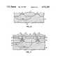
- a gate oxide 18 and polycrystalline silicon gate electrode 19are shown disposed above and between source and drain regions 20 and 21 of the n-channel device p-well 13.
- the source and drain regionsare formed in self-alignment with gate 19 and field oxide 17.
- gate oxide 22 and polysilicon gate electrode 23 for the p-channel deviceare shown disposed with the source and drain regions 24 and 25 which are, in turn, formed in self-alignment with field oxide 17. Leads 27 can then be applied which are isolated by oxide layer 29 and the structure completed by passivation layer 28.
- the ion implantation 14 carried out in conjunction with reference to FIG. 4is applied uniformly over the surface of the silicon substrate and is thus implanted into the p-well region without additional masks.
- This implantationsignificantly reduces or eliminates weak field regions which appear laterally in prior art p-well structures. It further substantially reduces weak field inversion regions and thus stray leakage channels from polysilicon or metal electrodes placed atop the areas.
- both the n-channel and p-channel field regionsare made without using extra masks other than the standard p-well masks shown in FIG. 2.
Landscapes
- Engineering & Computer Science (AREA)
- Physics & Mathematics (AREA)
- Condensed Matter Physics & Semiconductors (AREA)
- General Physics & Mathematics (AREA)
- Manufacturing & Machinery (AREA)
- Computer Hardware Design (AREA)
- Microelectronics & Electronic Packaging (AREA)
- Power Engineering (AREA)
- Metal-Oxide And Bipolar Metal-Oxide Semiconductor Integrated Circuits (AREA)
Abstract
Description
Claims (15)
Priority Applications (2)
| Application Number | Priority Date | Filing Date | Title |
|---|---|---|---|
| US06/757,331US4713329A (en) | 1985-07-22 | 1985-07-22 | Well mask for CMOS process |
| JP61169948AJPS6225452A (en) | 1985-07-22 | 1986-07-21 | CMOS transistor manufacturing method |
Applications Claiming Priority (1)
| Application Number | Priority Date | Filing Date | Title |
|---|---|---|---|
| US06/757,331US4713329A (en) | 1985-07-22 | 1985-07-22 | Well mask for CMOS process |
Publications (1)
| Publication Number | Publication Date |
|---|---|
| US4713329Atrue US4713329A (en) | 1987-12-15 |
Family
ID=25047393
Family Applications (1)
| Application Number | Title | Priority Date | Filing Date |
|---|---|---|---|
| US06/757,331Expired - LifetimeUS4713329A (en) | 1985-07-22 | 1985-07-22 | Well mask for CMOS process |
Country Status (2)
| Country | Link |
|---|---|
| US (1) | US4713329A (en) |
| JP (1) | JPS6225452A (en) |
Cited By (10)
| Publication number | Priority date | Publication date | Assignee | Title |
|---|---|---|---|---|
| US4889825A (en)* | 1986-03-04 | 1989-12-26 | Motorola, Inc. | High/low doping profile for twin well process |
| US4925806A (en)* | 1988-03-17 | 1990-05-15 | Northern Telecom Limited | Method for making a doped well in a semiconductor substrate |
| US4929565A (en)* | 1986-03-04 | 1990-05-29 | Motorola, Inc. | High/low doping profile for twin well process |
| US5030581A (en)* | 1986-09-27 | 1991-07-09 | Kabushiki Kaisha Toshiba | Method of fabricating a semiconductor apparatus |
| US5154946A (en)* | 1990-09-27 | 1992-10-13 | Motorola, Inc. | CMOS structure fabrication |
| US5350492A (en)* | 1992-09-18 | 1994-09-27 | Advanced Micro Devices, Inc. | Oxide removal method for improvement of subsequently grown oxides |
| FR2714525A1 (en)* | 1993-12-28 | 1995-06-30 | Fujitsu Ltd | Method for manufacturing a semiconductor device comprising metal-oxide-semiconductor field effect transistors. |
| US5759881A (en)* | 1993-09-10 | 1998-06-02 | Micron Technology, Inc. | Low cost well process |
| US6287937B1 (en) | 1997-08-21 | 2001-09-11 | Micron Technology, Inc. | Method for simultaneous dopant driving and dielectric densification in making a semiconductor structure |
| US20060141690A1 (en)* | 2004-12-23 | 2006-06-29 | Hynix Semiconductor Inc. | Method for manufacturing a semiconductor device |
Families Citing this family (2)
| Publication number | Priority date | Publication date | Assignee | Title |
|---|---|---|---|---|
| JPH0698401B2 (en)* | 1989-09-29 | 1994-12-07 | 川崎製鉄株式会社 | Welded steel pipe strip edge forming roll |
| JPH05154563A (en)* | 1991-12-10 | 1993-06-22 | Nippon Steel Corp | Roll device for forming welded pipe |
Citations (27)
| Publication number | Priority date | Publication date | Assignee | Title |
|---|---|---|---|---|
| US3876472A (en)* | 1974-04-15 | 1975-04-08 | Rca Corp | Method of achieving semiconductor substrates having similar surface resistivity |
| US3983620A (en)* | 1975-05-08 | 1976-10-05 | National Semiconductor Corporation | Self-aligned CMOS process for bulk silicon and insulating substrate device |
| US4013484A (en)* | 1976-02-25 | 1977-03-22 | Intel Corporation | High density CMOS process |
| US4043025A (en)* | 1975-05-08 | 1977-08-23 | National Semiconductor Corporation | Self-aligned CMOS process for bulk silicon and insulating substrate device |
| US4045259A (en)* | 1976-10-26 | 1977-08-30 | Harris Corporation | Process for fabricating diffused complementary field effect transistors |
| US4047284A (en)* | 1975-05-08 | 1977-09-13 | National Semiconductor Corporation | Self-aligned CMOS process for bulk silicon and insulating substrate device |
| US4131907A (en)* | 1977-09-28 | 1978-12-26 | Ouyang Paul H | Short-channel V-groove complementary MOS device |
| US4135955A (en)* | 1977-09-21 | 1979-01-23 | Harris Corporation | Process for fabricating high voltage cmos with self-aligned guard rings utilizing selective diffusion and local oxidation |
| US4143388A (en)* | 1976-05-18 | 1979-03-06 | Matsushita Electric Industrial Co., Ltd. | Mos type semiconductor device |
| US4152717A (en)* | 1975-07-18 | 1979-05-01 | Tokyo Shibaura Electric Co., Ltd. | Complementary MOSFET device |
| US4183134A (en)* | 1977-02-15 | 1980-01-15 | Westinghouse Electric Corp. | High yield processing for silicon-on-sapphire CMOS integrated circuits |
| US4282648A (en)* | 1980-03-24 | 1981-08-11 | Intel Corporation | CMOS process |
| US4295266A (en)* | 1980-06-30 | 1981-10-20 | Rca Corporation | Method of manufacturing bulk CMOS integrated circuits |
| US4306916A (en)* | 1979-09-20 | 1981-12-22 | American Microsystems, Inc. | CMOS P-Well selective implant method |
| US4314857A (en)* | 1979-07-31 | 1982-02-09 | Mitel Corporation | Method of making integrated CMOS and CTD by selective implantation |
| US4335504A (en)* | 1980-09-24 | 1982-06-22 | Rockwell International Corporation | Method of making CMOS devices |
| US4372033A (en)* | 1981-09-08 | 1983-02-08 | Ncr Corporation | Method of making coplanar MOS IC structures |
| US4373253A (en)* | 1981-04-13 | 1983-02-15 | National Semiconductor Corporation | Integrated CMOS process with JFET |
| US4376336A (en)* | 1980-08-12 | 1983-03-15 | Tokyo Shibaura Denki Kabushiki Kaisha | Method for fabricating a semiconductor device |
| US4382827A (en)* | 1981-04-27 | 1983-05-10 | Ncr Corporation | Silicon nitride S/D ion implant mask in CMOS device fabrication |
| US4385947A (en)* | 1981-07-29 | 1983-05-31 | Harris Corporation | Method for fabricating CMOS in P substrate with single guard ring using local oxidation |
| US4391650A (en)* | 1980-12-22 | 1983-07-05 | Ncr Corporation | Method for fabricating improved complementary metal oxide semiconductor devices |
| US4409726A (en)* | 1982-04-08 | 1983-10-18 | Philip Shiota | Method of making well regions for CMOS devices |
| US4412375A (en)* | 1982-06-10 | 1983-11-01 | Intel Corporation | Method for fabricating CMOS devices with guardband |
| US4420872A (en)* | 1980-12-23 | 1983-12-20 | U.S. Philips Corporation | Method of manufacturing a semiconductor device |
| US4517731A (en)* | 1983-09-29 | 1985-05-21 | Fairchild Camera & Instrument Corporation | Double polysilicon process for fabricating CMOS integrated circuits |
| US4567640A (en)* | 1984-05-22 | 1986-02-04 | Data General Corporation | Method of fabricating high density CMOS devices |
- 1985
- 1985-07-22USUS06/757,331patent/US4713329A/ennot_activeExpired - Lifetime
- 1986
- 1986-07-21JPJP61169948Apatent/JPS6225452A/enactivePending
Patent Citations (27)
| Publication number | Priority date | Publication date | Assignee | Title |
|---|---|---|---|---|
| US3876472A (en)* | 1974-04-15 | 1975-04-08 | Rca Corp | Method of achieving semiconductor substrates having similar surface resistivity |
| US4047284A (en)* | 1975-05-08 | 1977-09-13 | National Semiconductor Corporation | Self-aligned CMOS process for bulk silicon and insulating substrate device |
| US3983620A (en)* | 1975-05-08 | 1976-10-05 | National Semiconductor Corporation | Self-aligned CMOS process for bulk silicon and insulating substrate device |
| US4043025A (en)* | 1975-05-08 | 1977-08-23 | National Semiconductor Corporation | Self-aligned CMOS process for bulk silicon and insulating substrate device |
| US4152717A (en)* | 1975-07-18 | 1979-05-01 | Tokyo Shibaura Electric Co., Ltd. | Complementary MOSFET device |
| US4013484A (en)* | 1976-02-25 | 1977-03-22 | Intel Corporation | High density CMOS process |
| US4143388A (en)* | 1976-05-18 | 1979-03-06 | Matsushita Electric Industrial Co., Ltd. | Mos type semiconductor device |
| US4045259A (en)* | 1976-10-26 | 1977-08-30 | Harris Corporation | Process for fabricating diffused complementary field effect transistors |
| US4183134A (en)* | 1977-02-15 | 1980-01-15 | Westinghouse Electric Corp. | High yield processing for silicon-on-sapphire CMOS integrated circuits |
| US4135955A (en)* | 1977-09-21 | 1979-01-23 | Harris Corporation | Process for fabricating high voltage cmos with self-aligned guard rings utilizing selective diffusion and local oxidation |
| US4131907A (en)* | 1977-09-28 | 1978-12-26 | Ouyang Paul H | Short-channel V-groove complementary MOS device |
| US4314857A (en)* | 1979-07-31 | 1982-02-09 | Mitel Corporation | Method of making integrated CMOS and CTD by selective implantation |
| US4306916A (en)* | 1979-09-20 | 1981-12-22 | American Microsystems, Inc. | CMOS P-Well selective implant method |
| US4282648A (en)* | 1980-03-24 | 1981-08-11 | Intel Corporation | CMOS process |
| US4295266A (en)* | 1980-06-30 | 1981-10-20 | Rca Corporation | Method of manufacturing bulk CMOS integrated circuits |
| US4376336A (en)* | 1980-08-12 | 1983-03-15 | Tokyo Shibaura Denki Kabushiki Kaisha | Method for fabricating a semiconductor device |
| US4335504A (en)* | 1980-09-24 | 1982-06-22 | Rockwell International Corporation | Method of making CMOS devices |
| US4391650A (en)* | 1980-12-22 | 1983-07-05 | Ncr Corporation | Method for fabricating improved complementary metal oxide semiconductor devices |
| US4420872A (en)* | 1980-12-23 | 1983-12-20 | U.S. Philips Corporation | Method of manufacturing a semiconductor device |
| US4373253A (en)* | 1981-04-13 | 1983-02-15 | National Semiconductor Corporation | Integrated CMOS process with JFET |
| US4382827A (en)* | 1981-04-27 | 1983-05-10 | Ncr Corporation | Silicon nitride S/D ion implant mask in CMOS device fabrication |
| US4385947A (en)* | 1981-07-29 | 1983-05-31 | Harris Corporation | Method for fabricating CMOS in P substrate with single guard ring using local oxidation |
| US4372033A (en)* | 1981-09-08 | 1983-02-08 | Ncr Corporation | Method of making coplanar MOS IC structures |
| US4409726A (en)* | 1982-04-08 | 1983-10-18 | Philip Shiota | Method of making well regions for CMOS devices |
| US4412375A (en)* | 1982-06-10 | 1983-11-01 | Intel Corporation | Method for fabricating CMOS devices with guardband |
| US4517731A (en)* | 1983-09-29 | 1985-05-21 | Fairchild Camera & Instrument Corporation | Double polysilicon process for fabricating CMOS integrated circuits |
| US4567640A (en)* | 1984-05-22 | 1986-02-04 | Data General Corporation | Method of fabricating high density CMOS devices |
Cited By (11)
| Publication number | Priority date | Publication date | Assignee | Title |
|---|---|---|---|---|
| US4889825A (en)* | 1986-03-04 | 1989-12-26 | Motorola, Inc. | High/low doping profile for twin well process |
| US4929565A (en)* | 1986-03-04 | 1990-05-29 | Motorola, Inc. | High/low doping profile for twin well process |
| US5030581A (en)* | 1986-09-27 | 1991-07-09 | Kabushiki Kaisha Toshiba | Method of fabricating a semiconductor apparatus |
| US4925806A (en)* | 1988-03-17 | 1990-05-15 | Northern Telecom Limited | Method for making a doped well in a semiconductor substrate |
| US5154946A (en)* | 1990-09-27 | 1992-10-13 | Motorola, Inc. | CMOS structure fabrication |
| US5350492A (en)* | 1992-09-18 | 1994-09-27 | Advanced Micro Devices, Inc. | Oxide removal method for improvement of subsequently grown oxides |
| US5759881A (en)* | 1993-09-10 | 1998-06-02 | Micron Technology, Inc. | Low cost well process |
| FR2714525A1 (en)* | 1993-12-28 | 1995-06-30 | Fujitsu Ltd | Method for manufacturing a semiconductor device comprising metal-oxide-semiconductor field effect transistors. |
| US6287937B1 (en) | 1997-08-21 | 2001-09-11 | Micron Technology, Inc. | Method for simultaneous dopant driving and dielectric densification in making a semiconductor structure |
| US20060141690A1 (en)* | 2004-12-23 | 2006-06-29 | Hynix Semiconductor Inc. | Method for manufacturing a semiconductor device |
| US7186631B2 (en)* | 2004-12-23 | 2007-03-06 | Hynix Semiconductor Inc. | Method for manufacturing a semiconductor device |
Also Published As
| Publication number | Publication date |
|---|---|
| JPS6225452A (en) | 1987-02-03 |
Similar Documents
| Publication | Publication Date | Title |
|---|---|---|
| US4013484A (en) | High density CMOS process | |
| US5438007A (en) | Method of fabricating field effect transistor having polycrystalline silicon gate junction | |
| US6163053A (en) | Semiconductor device having opposite-polarity region under channel | |
| US4566175A (en) | Method of making insulated gate field effect transistor with a lightly doped drain using oxide sidewall spacer and double implantations | |
| US5334870A (en) | Complementary MIS transistor and a fabrication process thereof | |
| US5548143A (en) | Metal oxide semiconductor transistor and a method for manufacturing the same | |
| US4745079A (en) | Method for fabricating MOS transistors having gates with different work functions | |
| US4599118A (en) | Method of making MOSFET by multiple implantations followed by a diffusion step | |
| US5688722A (en) | CMOS integrated circuit with reduced susceptibility to PMOS punchthrough | |
| US3898105A (en) | Method for making FET circuits | |
| US5041885A (en) | Surface field effect transistor with depressed source and/or drain areas for ULSI integrated devices | |
| US4637124A (en) | Process for fabricating semiconductor integrated circuit device | |
| US4891326A (en) | Semiconductor device and a process for manufacturing the same | |
| JPH01101662A (en) | Manufacture of cmos device | |
| US4212683A (en) | Method for making narrow channel FET | |
| US4713329A (en) | Well mask for CMOS process | |
| JPS58147074A (en) | Metal oxide semiconductor transistor device and its manufacturing method | |
| US4131907A (en) | Short-channel V-groove complementary MOS device | |
| US20040041170A1 (en) | Low dose super deep source/drain implant | |
| KR940000521B1 (en) | Semiconductor integrated circuit device and its manufacturing method | |
| US4485390A (en) | Narrow channel FET | |
| EP0091256B1 (en) | Cmos device | |
| JPS55151363A (en) | Mos semiconductor device and fabricating method of the same | |
| US4567640A (en) | Method of fabricating high density CMOS devices | |
| JP2860482B2 (en) | Method for manufacturing semiconductor device |
Legal Events
| Date | Code | Title | Description |
|---|---|---|---|
| AS | Assignment | Owner name:SILICON SYSTEMS, INC., 14351 MYFORD ROAD, TUSTIN, Free format text:ASSIGNMENT OF ASSIGNORS INTEREST.;ASSIGNOR:LIANG, VICTOR;REEL/FRAME:004487/0503 Effective date:19850911 Owner name:DATA GENERAL CORPORATION, 4400 COMPUTER DRIVE, WES Free format text:ASSIGNMENT OF ASSIGNORS INTEREST.;ASSIGNOR:FARB, JOSEPH;REEL/FRAME:004487/0502 Effective date:19850715 Owner name:SILICON SYSTEMS, INC., 14351 MYFORD ROAD, TUSTIN, Free format text:ASSIGNMENT OF ASSIGNORS INTEREST.;ASSIGNOR:FARB, JOSEPH;REEL/FRAME:004487/0502 Effective date:19850715 Owner name:SILICON SYSTEMS, INC., 14351 MYFORD ROAD, TUSTIN, Free format text:ASSIGNMENT OF ASSIGNORS INTEREST.;ASSIGNOR:HSU, CHUNG;REEL/FRAME:004487/0501 Effective date:19850718 Owner name:DATA GENERAL CORPORATION, 4400 COMPUTER DRIVE, WES Free format text:ASSIGNMENT OF ASSIGNORS INTEREST.;ASSIGNOR:HSU, CHUNG;REEL/FRAME:004487/0501 Effective date:19850718 Owner name:DATA GENERAL CORPORATION, 4400 COMPUTER DRIVE, WES Free format text:ASSIGNMENT OF ASSIGNORS INTEREST.;ASSIGNOR:LIANG, VICTOR;REEL/FRAME:004487/0503 Effective date:19850911 | |
| AS | Assignment | Owner name:SILICON SYSTEMS, INC., 14351 MYFORD ROAD, TUSTIN, Free format text:ASSIGNMENT OF ASSIGNORS INTEREST.;ASSIGNORS:FANG, ROBERT;WANG, JERRY;REEL/FRAME:004482/0777 Effective date:19850628 Owner name:DATA GENERAL CORPORATION, 4400 COMPUTER DRIVE, WES Free format text:ASSIGNMENT OF ASSIGNORS INTEREST.;ASSIGNORS:FANG, ROBERT;WANG, JERRY;REEL/FRAME:004482/0777 Effective date:19850628 | |
| STCF | Information on status: patent grant | Free format text:PATENTED CASE | |
| CC | Certificate of correction | ||
| FEPP | Fee payment procedure | Free format text:PAYOR NUMBER ASSIGNED (ORIGINAL EVENT CODE: ASPN); ENTITY STATUS OF PATENT OWNER: LARGE ENTITY | |
| FPAY | Fee payment | Year of fee payment:4 | |
| FPAY | Fee payment | Year of fee payment:8 | |
| FPAY | Fee payment | Year of fee payment:12 |