US4712190A - Self-timed random access memory chip - Google Patents
Self-timed random access memory chipDownload PDFInfo
- Publication number
- US4712190A US4712190AUS06/694,874US69487485AUS4712190AUS 4712190 AUS4712190 AUS 4712190AUS 69487485 AUS69487485 AUS 69487485AUS 4712190 AUS4712190 AUS 4712190A
- Authority
- US
- United States
- Prior art keywords
- signal
- data
- signals
- chip
- output
- Prior art date
- Legal status (The legal status is an assumption and is not a legal conclusion. Google has not performed a legal analysis and makes no representation as to the accuracy of the status listed.)
- Expired - Lifetime
Links
Images


Classifications
- G—PHYSICS
- G11—INFORMATION STORAGE
- G11C—STATIC STORES
- G11C7/00—Arrangements for writing information into, or reading information out from, a digital store
- G11C7/22—Read-write [R-W] timing or clocking circuits; Read-write [R-W] control signal generators or management
- G—PHYSICS
- G06—COMPUTING OR CALCULATING; COUNTING
- G06F—ELECTRIC DIGITAL DATA PROCESSING
- G06F13/00—Interconnection of, or transfer of information or other signals between, memories, input/output devices or central processing units
- G06F13/38—Information transfer, e.g. on bus
- G06F13/42—Bus transfer protocol, e.g. handshake; Synchronisation
- G06F13/4204—Bus transfer protocol, e.g. handshake; Synchronisation on a parallel bus
- G06F13/4234—Bus transfer protocol, e.g. handshake; Synchronisation on a parallel bus being a memory bus
- G06F13/4243—Bus transfer protocol, e.g. handshake; Synchronisation on a parallel bus being a memory bus with synchronous protocol
Definitions
- the inventionrelates generally to the field of integrated circuit chips for use in digital data processing systems, and more specifically to random access memory (RAM) chips used in various portions of such systems to store digital data for processing or other purposes, such as control or the like.
- RAMrandom access memory
- RAMrandom access memory
- CPUcentral processing unit
- RAM chipsare also used in, for example, translation buffers in the CPU that are used in translating from virtual to physical addresses in computer systems employing virtual memory techniques.
- RAM chipsmay also be used in, for example, writable control stores used to store microcode sequences for processing of instructions, and in similar data storage areas in the CPUs.
- a major problem with current random access memory chipsis that they require the external circuitry to supply a number of input signals having fairly complex relative timing requirements and to maintain them in the required conditions throughout the storage or retrieval operation in order to operate properly.
- the random access memory (RAM) chipsreceive data and address signals from a plurality of data and address registers, and also receive read/write and depending on the particular chips, other operation control signals. If the required operation is a read operation, the RAM also transmits the read data to a data output register, which latches the read data and makes it available to other circuitry in the computer system.
- the operation of the memory systemis limited by the potential skew of the numerous signals transmitted to and from the RAM, by the set-up times required for the signals to shift, if necessary, between negated and asserted conditions, and also by the circuit delays inherent in the operation of the circuits themselves.
- the off-chip registers and control signal generation circuitrymust maintain the address, data (if a write operation) and control signals at the required levels during the entire memory operation.
- the inventionprovides a new and improved random access memory chip having a random access memory in addition to input and output storage registers for storing input data, address and control information and circuitry for generating a storage/retrieval enabling signal for enabling the data to be stored at specified addresses or retrieving data from the specified addresses in the memory, all on the single chip.
- the inventionprovides a RAM chip having a plurality of addressable storage locations, a plurality of input registers each for receiving and latching data, address, and control signals, as well as an output register for receiving data during a retrieval operation from an addressed storage location and transmitting the stored data to an output terminal on the chip.
- the chipalso receives, from external circuitry, a clock signal which synchronizes the latching of the data, address, and control signals, which also synchronizes the beginning of the on-chip generation of the internally generated control signals that control the storage of data in the addressed locations or the transmission of data therefrom.
- Placing the input registers, output register and control signal generating circuitry on the RAM chip, all being responsive to the system clock signal,allows the chip to be operated in a pipelined manner when connected in a system between off-chip input address and data registers and an output data register. Placing registers onto the chip greatly reduces the skew and set up times for the signals between the on-chip registers and the actual memory circuitry, allowing the chip to operate quite fast. Further, when operated in a pipelined manner, the skew and set-up times for the off-chip signals can take place for a subsequent memory operation, while the chip is performing a current operation.
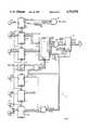
- FIG. 1is a block diagram of a self-timed random access memory circuit for use on a single chip constructed in accordance with the invention
- FIG. 2Ais a logic diagram detailing a write enabling signal generator useful in the circuit depicted on FIG. 1, and FIG. 2B is a timing diagram which is useful in understanding the operation of the circuit depicted in FIG. 2A;
- FIG. 3is a logic diagram of an output register which is useful in connection with the circuit depicted on FIG. 1;
- FIGS. 4A and 4Bare timing diagrams useful in understanding the operation of the circuit depicted on FIG. 1;
- FIG. 5is an alternate embodiment of an output register which is useful in the circuit depicted in FIG. 1;
- FIG. 6Ais a block diagram depicting a system including multiple self-timed random access memory chips as depicted in FIG. 1 in a memory subsystem
- FIG. 6Bis a timing diagram that is useful in understanding the operation of the system depicted in FIG. 6A.
- the inventionprovides a new and improved self-timed random access memory (RAM) circuit 10 residing on a single integrated circuit chip.
- the self-timed RAM circuitincludes a random access memory (RAM) 11 which includes a plurality of addressable storage locations.
- the RAM 11includes 256 locations of four bits each.
- the RAM 11receives data, address, and bit write enable signals through respective input terminals 12, 13 and 14, and transmits data signals through an output terminal 15.
- Terminals 17 and 20represent input terminals to the chip on which the self-timed RAM circuit 10 resides, the DATA IN and CLK clocking signals being provided by circuitry external to the chip.
- the number of lines for carrying the DATA IN (N:0) and the DATA LTH IN (N:0) signalscorresponds to the number of bits in each storage location.
- the address signals coupled to address input terminal 13 of RAM 11comprise ADRS LTH IN latched address in signals provided by a register 21.
- the register 21receives ADRS IN signals from terminals 22.
- the ADRS IN signalsare latched in register 21 in response to the CLK clock signal from terminal 20.
- the number of ADRS LTH IN signals coupled in parallel to address in terminals 13are determined by the number of addressable locations in RAM 11. In the embodiment in which RAM 11 has 256 locations, the ADRS LTH IN signals comprise eight individual signals provided in parallel. The signals are binary-encoded and are decoded in circuitry in RAM 11 to identify a single storage location.
- the clock signal received at terminal 20also controls a register 23 which receives a WRT write signal from a terminal 24.
- the WRT write signalidentifies the operation, namely a read or a write operation, to be performed in connection with the location identified by the ADRS IN signals that are contemporaneously latched in register 21.
- the output signal from register 23, namely, a WRT LTH latched write signalis used by control circuitry described below to control the generation of signals received at bit write enable terminals 14 to control writing in RAM 11.
- the RAM 11In response to asserted signals at the bit write enable terminals 14, the RAM 11 stores the DATA LTH IN (N:0) data signals in respective bit locations of the location identified by the ADRS LTH IN (N:0) address signals. If, however, the signals at the bit write enable terminals 14 are negated, the respective bit locations of the addressed location are read and the data stored therein is transmitted through output terminals 15 as RAM DATA OUT (N:0) signals.
- the CLK clock signalalso controls a register 25 which receives BIT EN bit enabling signals from an input terminal 26.
- the signals stored in register 25are transmitted as BIT LTH EN latched bit enabling signals.
- each addressable storage locationcomprises bit storage locations, and the BIT EN signals comprise a like number of individual signals, each of which is associated with one of the bit locations in the storage locations of RAM 11.
- the clock signalalso controls a register 27 which receives a CHP EN chip enabling signal from a terminal 30.
- the register 27transmits a CHP LTH EN latched chip enabling signal.
- the CHP LTH EN latched chip enabling signalis negated, the circuit 10 is disabled from operating.
- the CLK clock signal received at terminal 20also controls a register 31, which receives and stores a CLK EN clock enabling signal from a terminal 32.
- Register 31provides a CLK LTH EN latched clock enabling output signal, which, when asserted, enables portions of the circuitry of the self-timed RAM circuit 10 to operate, as explained below.
- self-timed RAM circuit 10includes an output register 33 which receives MASK DATA OUT (N:0) mask data out signals.
- the MASK DATA OUT (N:0) signalsare derived from the RAM DATA OUT (N:0) signals from RAM 11 as explained below.
- Output register 33transmits DATA OUT output data signals to output terminals 34.
- off-chip circuitryWhen off-chip circuitry is to store data in or retrieve data from self-timed RAM circuit 10, it transmits the respective data address and control input signals to terminals 17, 22, 24, 26, 30 and 32 and asserts the CLK clock timing signal which is received at terminal 20. The input signals are then latched in registers 16, 21, 23, 25, 27 and 31. If the WRT write signal is asserted, the register 23 transmits an asserted WRT LTH latched write signal to an AND gate 35, which transmits a WRT EN write enabling signal a short time later, the delay being determined by a delay line 36, if the CLK LTH EN latched clock enabling signal from register 31 is asserted.
- the input signal to delay line 36is the CLK clock signal from terminal 20, and the delay line is provided to time the WRT EN signal so as to correctly position, in time, the write enable signals at terminals 14 of RAM 11.
- the output of the delay line 36comprises a DLY CLK delayed clocking signal, which provides the third input signal to AND gate 35.
- the WRT EN write enabling signalis transmitted to a write pulse generator 37, the circuit for which is depicted in FIG. 2A.
- the write pulse generatorcomprises an AND gate 40 which receives at one input terminal 40a the WRT EN write enabling signal directly, and at the other input terminal 40b a signal from a set of serially-connected gates followed by an inverter generally indicated by the reference numeral 41.
- the output signal of AND gate 40namely, signal A, is transmitted to an input terminal 44a of AND gate 44, and also to a second series of gates generally indicated by the reference numeral 42.
- the B output signal from the output terminal of the last of gates 42is transmitted through an inverter 43 to the second input terminal 44b of an AND gate 44.
- the B output signal from the last of gates 42is also transmitted to one input terminal of a NOR gate 45b, which is connected to a NOR gate 45a to form a flip-flop 45.
- the other input signal to the NOR gates comprising flip-flop 45is provided by the signal from the output terminal of AND gate 44; specifically, the output terminal of AND gate 44 is connected to an input terminal of NOR gate 45a.
- the output signal of flip-flop 45, at output terminal 46 of NOR gate 45ais complemented through an inverter 50 as the WR PLS write pulse signal.
- the write pulse generator 37also receives the CLK clock signal, which enables an AND gate 51 and a set of gates followed by an inverter 52 to assert a C pulse signal.
- the C pulse signalis coupled to an input of NOR gate 45b to establish an initial condition for the flip-flop, most particularly when the chip 10 is initially powered up.
- the operation of the circuit depicted in FIG. 2B of the write pulse generator circuit 37is as follows.
- the output signal of gates 41 at terminal 40Bis at a high (asserted) level. Accordingly, signal A and B are both at low (negated) levels.
- NOR gate 45Ais energized so that the output signal at terminal 46 is at a high level
- NOR gate 45Bis deenergized so that the output signal at its output terminal 47 is at a low level.
- thisis enabled by the asserted C signal from AND gate 51. Accordingly, when the signal at node 46 is complemented by the inverter 50, the resulting WR PLS write pulse signal is at a low level.
- the time delay provided by gates 41determines the length of the assertion of the A and B signals. For a time determined by the gate delay of gates 41, the A signal remains high. However, when the asserted WRT EN write enabling signal propagates to input terminal 40B through gates 41, the A signal goes low, deenergizing AND gate 44 and forcing the signal provided by it to the connected terminal of NOR gate 45a to a low condition. However, since the signal at terminal 47 is high, NOR gate 45A remains deenergized, the signal at node 46 remains low, and the WR PLS signal provided by inverter 50 remains high. Since the leading and trailing edges of the B signal are both delayed by gates 42 by the same amount of time, the length of assertion of the B signal is the same as the length of assertion of the A signal.
- the gate delay of gates 42determines the length of the WR PLS write pulse signal.
- the B signalgoes to a high (asserted) condition, driving both the input signal to input terminal 44b of AND gate 44 and the signal at terminal 47 to a low (negated) condition.
- the first to be asserted of the output signal from AND gate 44 or the signal at terminal 47drives the output signal of NOR gate 45a to a high (asserted) condition, which, in turn, drives the WR PLS signal to a negated state, as depicted in FIG. 2B.
- the length of and spacing between the A and B signalsdetermine the speed with which the WR PLS write pulse signal can be repeated.
- the B signalis returned to a low (negated) condition.
- NOR gate 45bmaintains the signal at terminal 47 in the low condition.
- the sequence of operationscan repeat at the next assertion of the WRT EN write enabling signal.
- gates 51 and 52is similar to the operation of gates 40 and 41. After the initial condition of flip-flop 45 is determined by the C signal when the chip is initially powered. Thereafter, the conditions of the flip-flop are determined by the A and B signals, and the C signal is essentially redundant of the B signal, since, when the C signal is asserted, the B signal has already forced flip-flop 45 into a condition in which the WR PLS signal is negated.
- the BIT LTH EN (N:0) latched bit enabling signalsare transmitted to a set of AND gates represented by gate 60.
- One input terminal of each of the AND gatesreceives one of the BIT LTH EN signals as well as the CHP LTH EN latched chip enable signal from register 27.
- the respective ones of gates 60 which also receive an asserted BIT LTH EN signalare energized to transmit asserted BIT MASK (N:0) bit mask signals.
- the BIT MASK (N:0) signalsare transmitted to a set of AND gates represented by gate 61.
- One input terminal of each of the AND gatesreceives one of the BIT MASK (N:0) signals.
- the other input terminal of all of the gatesalso receives the WR PLS write pulse signal from the write pulse generator 37.
- the ones of gates 61 receiving asserted BIT MASK (N:0) signalsare energized to assert respective ones of the WE (N:0) write enable signals to energize corresponding ones of the bit write enable terminals 14.
- the BIT MASK (N:0) signalsare also transmitted to a set of gates generally indicated by reference numeral 62, which also receives the RAM DATA OUT (N:0) signals from RAM 11.
- the MASK DATA OUT (N:0) output signals from gates 62are coupled to the output register 33 and are latched in response to the CLK clocking signal, CLK LTH EN latch clock enabling signal, WRT LTH latched write signal and an LTH MODE latch mode signal provided by external circuitry at terminal 62 of the chip.
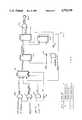
- FIG. 3contains a detailed logic diagram of gates 62 and output register 33.
- the gates 62comprise a plurality of individual AND gates 62(N) through 62(0), each of which includes an input terminal which receives a corresponding RAM DATA OUT (N) through (0) signal from RAM 11.
- the other input terminal of each ANDgatereceives the corresponding BIT MASK (N) through (0) from gates 60.
- the output register 33includes a number of stages 70(0) through 70(N), each of which includes an input multiplexer 71(0) through 71(N) which receives, at one input thereof, the MASK DATA OUT (0) through (N) signals from gates 62(0) through 62(N).
- the output signals from multiplexers 71(0) through 71(N)are coupled to the "D" data input terminals of latches 72(0) through 72(N).
- the Q output terminals of the respective latches 72(0) through 72(N), through which LTH MASK DATA (N:0) latched mask data signals are transmitted,are connected to the "D" data input terminals of latches 73(0) through 73(N) and 74(0) through 74(N).
- All of the latches 72(0) through 72(N), 73(0) through 73(N) and 74(0) through 74(N)are level-sensitive latches which pass the signals at the respective D input terminal to a Q output terminal when a latch signal at an L input terminal is at a negated level, and latch and hold the signal at the D input terminal when the latch signal at the L input terminal is at an asserted level.
- the LTH MODE latch mode signalenables output register 33 to operate in two modes depending on the asserted or negated condition of the signal.
- the latches 72(0) through 72(N)latch the signals at the input terminals when the CLK clock signal is asserted, and the latches 73(0) through 73(N) and latch the LTH MASK DATA (N:0) signals previously latched in latches 72(0) through 72(N) when the CLK clock signal is next negated.
- the latches 74(0) through 74(N)are essentially transparent, as they do not latch the signals.
- the MASK DATA OUT (N:0) signalsare also latched by latches 72(0) through 72(N) when the CLK clock signal is asserted, and the latches 73(0) through 73(N) and 74(0), through 74(N) to latch the LTH MASK DATA (N:0) signals from latches 72(0) through 72(N) when the clock signal is next negated.
- the latches 72(0) through 72(N)act as master latches
- the latches 73(0) through 73(N) and 74(0) through 74(N)act as slave latches, of master-slave latches.
- Latches 73(0) through 73(N)are controlled by a HOLD LTH hold latch signal generated by an inverter 80.
- the HOLD LTH signalis the complement of the CLK clock signal.
- Latches 74(0) through 74(N)are controlled by an OUT LTH output latch signal from an OR gate 81 and inverter 82.
- the LTH MODE latch mode signalis negated, the OUT LTH signal is asserted and negated in response to complementary transitions of the CLK timing signal.
- the latches 74(0) through 74(N)latch the LTH MASK DATA (N:0) signals from latches 72(0) through 72(N) when the CLK timing signal is negated, and pass them when the CLK signal is asserted.
- the LTH MODE latch mode signalis negated, gate 81 is always energized and the OUT LTH signal is always negated. Accordingly, the output signals from latches 74(0) through 74(N) always follow the LTH MASK DATA (N:0) input signals from latches 72(0) through 72(N). In this mode, the latches 74(0) through 74(N) have no effect on the circuit.
- the output signals from latches 74(0) through 74(N)are coupled to respective input terminals of a set of AND gates 75(0) through 75(N), whose output terminals are connected to the chip output terminals 34(0) through 34(N).
- AND gates 75(0) through 75(N)are enabled by a RD EN read enable signal from a flip-flop 76, which is set when the CLK clock signal is asserted if the CLK LTH EN signal is asserted, otherwise the CLK signal causes the flip-flop to be cleared.
- the RD EN read enable signalis asserted, allowing the output signals from latches 74(0) through 74(N) to be transmitted therethrough as the DATA OUT (N:0) signals; otherwise the signals from latches 74(0) through 74(N) are blocked.
- Latches 73(0) and 73(N)are provided in the embodiment of the output register 33 depicted in FIG. 3 since it is desired to maintain the previously retrieved data on the DATA OUT (N:0) signal lines while a subsequent write operation is taking place and when the CLK LTH EN latched clock enabling signal is negated. If a read operation is taking place, the WRT LTH latched write signal is negated. Accordingly, the multiplexers 71(0) through 71(N) couple the signal at the "0" input terminals to the output terminals for transmission to the respective latches 72(0) through 72(N). That data is latched in the latches 73(0) through 73(N) when the CLK clock signal from next negated.
- the output signals of latches 73(0) through 73(N), namely the HOLD MASK DATA (N:0) signalsare coupled to the respective "1" input terminals of multiplexers 71(0) through 71(N).
- the multiplexers 71(0) through 71(N)couple the previously-stored HOLD MASK DATA (N:0) signals to the input terminals of latches 72(0) through 72(N), maintaining the read data on the data out (0) through (N) signal lines to terminals 34(0) through 34(N).
- the chipis capable of pipelined operation. This is particularly evident in connection with read operations. Specifically, when the input signals for an operation are latched in response to the assertion of the CLK signal, the read data in response to the input signals that were latched in response to the previous assertion of the CLK clock signal is latched.
- the operation of the self-timed RAM chip depicted in FIG. 1can be made much faster in pipelined systems than prior RAM chips.
- the operation of the self-timed RAM chip depicted in FIG. 1is set forth in the timing diagram of FIG. 4A, when the LTH MODE latch mode signal is negated.
- the differences in operation when the LTH MODE latch mode signal is assertedwill be described in connection with FIG. 4B.
- FIG. 4Adepicts the timing of four successive cycles, denominated Cycle 0, Cycle 1, Cycle 2 and Cycle 3, of the CLK clock signal.
- Cycle 1a write request is received from off-chip, and during Cycles 0, 2 and 3, read requests are received.
- the latched ADRS IN signalsare coupled to respective input terminals 12 and 13 of RAM 11 when the CLK clock signal shifts to the asserted state, or more specifically, a short time thereafter as determined by the delays in the gates of registers 16 and 21 and in the lines connecting the registers to the RAM 11. Since the operation is a read operation, the condition of the DATA LTH IN (N:0) signals is irrelevant.
- Conventional address decoding circuitry in RAM 11selects the addressed location identified by the ADRS LTH IN signals.
- Conventional sense amplifiers in the output circuitry of the RAMdetermine the states of the signals from the selected location, that is whether they are asserted or negated, and transmit the RAM DATA OUT (N:0) signals in response thereto.
- the RAM DATA OUT (N:0) signalsare transmitted a short time after the transmission of the ADRS LTH IN signals to address input terminals 13 of RAM 11, the timing being dependent on delays inherent in the internal circuitry of RAM 11.
- the MASK DATA OUT (N:0) signalsare generated.
- the LTH MODE latch mode signalis negated and the CLK LTH EN signal is asserted
- the MASK DATA OUT (N:0) signalsis latched in latches 73(0) through 73(N) and 74(0) through 74(N) on the rising edge of the CLK clock signal marking the beginning of cycle 1.
- the CHP LTH EN signalis asserted
- flip-flop 76sets on the transition of the CLK signal marking the beginning of Cycle 1, and so the asserted RD EN read enabling signal enables AND gates 75(0) through 75(N), allowing the signals from latches 74(0) through 74(N) to be coupled to output terminals 34(0) through 34(N).
- the read data requested in cycle 0thus is available at the beginning of cycle 1.
- the WRT PLS signalenables the RAM 11 to store the DATA LTH IN (N:0) signals in the storage location specified by the ADRS LTH IN latched address in signals from register 21. Since the WRT LTH signal is asserted, the output register 33 maintains the DATA OUT (N:0) output data signals from cycle 1 through cycle 2.
- cycle 2a read operation is initiated, which progresses in the same way as the read operation in cycle 0.
- the CLK EN signalis negated, and at the transition of the CLK signal at the beginning of cycle 3, the CLK LTH EN latched clock enable signal is also negated.
- cycle 3a read operation is being requested by the external circuitry (not shown), but since the CLK LTH EN signal is negated, AND gate 83 is disabled during the next cycle (not shown) forcing the DATA OUT (N:0) data output signals to remain the same as in the previous cycle (that is, as in Cycle 3).
- the self-timed RAM 10(FIG. 1) when the LTH MODE signal is asserted will be described in connection with FIG. 4B.
- the read data requested at the beginning of one cycleis available at the beginning of the next cycle, but the data is initially latched, by latches 72(0) through 72(N), when the CLK clock signal falls to a low (negated) state.
- the latched LTH MASK DATA (N:0) signals from latches 72((0) through 72(N)are then latched in the latches 73(0) through 73(N) and 74(0) through 74(N) when the CLK clock signal next shifts to an asserted (high) condition.
- the LTH MASK DATA (N:0) latched mask data output signals from latches 72(0) through 72(N) signalscorrespond to the input signals from multiplexers 71(0) through 71(N).
- the modes controlled by the LTH MODE latch mode signalare provided to allow self-timed RAM 10 to accommodate to both high and low clock speeds.
- the LTH MODE signalis preferably negated.
- the CLK clock signalis at a relatively low speed, the LTH MODE signal is preferably asserted.
- the RAM DATA OUT (N:0) signals from RAM 11are latched in latches 72(0) through 72(N) on the falling edge of the CLK signal, not on the later rising edge as in the other mode, and so the RAM 11 does not have to maintain the RAM DATA OUT (N:0) signals for as long a time.
- FIG. 3maintains the read data as the DATA OUT (N:0) signals during a subsequent write operation.
- FIG. 5depicts a stage 70(i) useful in such a register if it is desired to couple write data through as the DATA OUT (N:0), and not maintain previous read data.
- the stageincludes latches 72(i), 73(i) and 74(i) and the register includes control circuitry 80, 81 and 82 as in the register depicted on FIG. 3.
- the stagealso includes an output AND gate 75(i) controlled by the RD EN signal from flip-flop 76 (FIG. 3).
- the stagealso includes an input multiplexer 90 which includes three data input terminals, one which receives the MASK DATA OUT (i) signal from the AND gate 62(i), whixh corresponds to the data bit from RAM 11 of the BIT MASK (i) signal is asserted. Another input terminal receives the HOLD MASK DATA (i) signal from latch 73(i) which will be used if the CLK LTH EN latched clock enable signal is asserted.
- the multiplexerreceives a MASK DATA IN (i) signal from and AND gate 91, which is the DATA LTH IN (i) write data bit from data input register 16, if the corresponding BIT MASK (i) is asserted.
- the multiplexerreceives two binary-encoded control signals, namely 51 and 52, which determines which input signal is coupled through as the MUX OUT signal to the data input of latch 72(i).
- the CLK LTH EN signalis negated
- the 52 signalis asserted by inverter 92 and the S1 signal generated by AND gate 93 is negated, and the HOLD MASK DATA (i) signal is passed by multiplexer 90. If the CLK LTH EN signal is asserted, the 52 signal is negated and the 51 signal from AND gate 91 control multiplexer 91.
- the S1 signalis also asserted, causing multiplexer 91 to couple the MASK DATA IN (i) signal to the input terminal of latch 72(i). Otherwise, a read operation is occurring and the S1 signal is negated, causing the multiplexer 80 to couple the MASK DATA OUT (i) signal to the data input terminal of latch 72(i).
- FIG. 6Aillustrates the use of the self-timed RAM chips as depicted in FIG. 1, in a system 100.
- the system 100includes a chip A 101 and chip B 102 connected to receive the input signals in parallel, except that the CHP EN chip enable signal transmitted to chip A 101 is complemented by means of an inverter 103.
- the respective DATA OUT (N:0) signals from chips A and Bare ORed together in a plurality of OR gates 104 to form DATA OUT COMP (N:0) composite data out signals.
- FIG. 6Bwhich presents a timing diagram illustrating the operation of system 100 (FIG.
Landscapes
- Engineering & Computer Science (AREA)
- Theoretical Computer Science (AREA)
- Physics & Mathematics (AREA)
- General Engineering & Computer Science (AREA)
- General Physics & Mathematics (AREA)
- Dram (AREA)
Abstract
Description
Claims (7)
Priority Applications (1)
| Application Number | Priority Date | Filing Date | Title |
|---|---|---|---|
| US06/694,874US4712190A (en) | 1985-01-25 | 1985-01-25 | Self-timed random access memory chip |
Applications Claiming Priority (1)
| Application Number | Priority Date | Filing Date | Title |
|---|---|---|---|
| US06/694,874US4712190A (en) | 1985-01-25 | 1985-01-25 | Self-timed random access memory chip |
Publications (1)
| Publication Number | Publication Date |
|---|---|
| US4712190Atrue US4712190A (en) | 1987-12-08 |
Family
ID=24790610
Family Applications (1)
| Application Number | Title | Priority Date | Filing Date |
|---|---|---|---|
| US06/694,874Expired - LifetimeUS4712190A (en) | 1985-01-25 | 1985-01-25 | Self-timed random access memory chip |
Country Status (1)
| Country | Link |
|---|---|
| US (1) | US4712190A (en) |
Cited By (33)
| Publication number | Priority date | Publication date | Assignee | Title |
|---|---|---|---|---|
| US4884198A (en)* | 1986-12-18 | 1989-11-28 | Sun Microsystems, Inc. | Single cycle processor/cache interface |
| US5033001A (en)* | 1986-12-19 | 1991-07-16 | Fujitsu Limited | Dual mode memory read cycle time reduction system which generates read data clock signals from shifted and synchronized trigger signals |
| DE4132833A1 (en)* | 1990-10-05 | 1992-04-09 | Digital Equipment Corp | HIERARCHIC CIRCUIT-INTEGRATED CACHE MEMORY |
| US5107462A (en)* | 1989-02-03 | 1992-04-21 | Digital Equipment Corporation | Self timed register file having bit storage cells with emitter-coupled output selectors for common bits sharing a common pull-up resistor and a common current sink |
| EP0379772A3 (en)* | 1989-01-27 | 1992-05-20 | Digital Equipment Corporation | Programmable data transfer timing |
| EP0360388A3 (en)* | 1988-08-25 | 1992-09-02 | Industrial Technology Research Institute | Method and apparatus for automatic address setting for recording and replay |
| EP0437160A3 (en)* | 1989-12-13 | 1993-01-13 | International Business Machines Corporation | Main storage memory cards having single bit set and reset functions |
| EP0438011A3 (en)* | 1990-01-18 | 1993-05-19 | International Business Machines Corporation | Logic on main storage memory cards for insertion and extraction of tag bits |
| US5276839A (en)* | 1991-03-07 | 1994-01-04 | United States Of America As Represented By The Secretary Of The Air Force | System for programming EEPROM with data loaded in ROM by sending switch signal to isolate EEPROM from host system |
| US5386585A (en)* | 1993-02-03 | 1995-01-31 | Intel Corporation | Self-timed data pipeline apparatus using asynchronous stages having toggle flip-flops |
| US5560000A (en)* | 1992-05-28 | 1996-09-24 | Texas Instruments Incorporated | Time skewing arrangement for operating memory in synchronism with a data processor |
| US5710910A (en)* | 1994-09-30 | 1998-01-20 | University Of Washington | Asynchronous self-tuning clock domains and method for transferring data among domains |
| EP0778578A3 (en)* | 1988-11-29 | 1998-02-18 | Matsushita Electric Industrial Co., Ltd. | A synchronous semiconductor memory integrated circuit, a method for accessing said memory and a system comprising such a memory |
| US5752270A (en)* | 1993-12-24 | 1998-05-12 | Mitsubishi Denki Kabushiki Kaisha | Method of executing read and write operations in a synchronous random access memory |
| US5754816A (en)* | 1993-09-27 | 1998-05-19 | Advanced Risc Machines Limited | Data storage apparatus and method with two stage reading |
| US5802548A (en)* | 1991-10-25 | 1998-09-01 | Chips And Technologies, Inc. | Software programmable edge delay for SRAM write enable signals on dual purpose cache controllers |
| USRE35921E (en)* | 1988-11-29 | 1998-10-13 | Matsushita Electric Industrial Co., Ltd. | Dynamic video RAM incorporating single clock random port control |
| EP0773549A3 (en)* | 1995-11-10 | 1998-12-02 | Nec Corporation | Synchronous semiconductor memory having a write execution time dependent upon a cycle time |
| US6018794A (en)* | 1997-04-30 | 2000-01-25 | Arm Limited | Data processing apparatus and method for generating timing signals for a self-timed circuit |
| US6075721A (en)* | 1997-12-18 | 2000-06-13 | Advanced Micro Devices, Inc. | Random access memory having bit selectable mask for memory writes |
| US20020087790A1 (en)* | 1995-10-19 | 2002-07-04 | Barth Richard Maurice | Memory integrated circuit device which samples data upon detection of a strobe signal |
| US6493789B2 (en) | 1995-10-19 | 2002-12-10 | Rambus Inc. | Memory device which receives write masking and automatic precharge information |
| US6529993B1 (en) | 2000-10-12 | 2003-03-04 | International Business Machines Corp. | Data and data strobe circuits and operating protocol for double data rate memories |
| US6546446B2 (en) | 1990-04-18 | 2003-04-08 | Rambus Inc. | Synchronous memory device having automatic precharge |
| US6591353B1 (en) | 1995-10-19 | 2003-07-08 | Rambus Inc. | Protocol for communication with dynamic memory |
| US6643793B1 (en)* | 1999-10-21 | 2003-11-04 | Oki Electric Industry Co., Ltd. | Apparatus for transferring and holding data based on a selected clock rate |
| US7177998B2 (en) | 2001-04-24 | 2007-02-13 | Rambus Inc. | Method, system and memory controller utilizing adjustable read data delay settings |
| US7197611B2 (en) | 1997-10-10 | 2007-03-27 | Rambus Inc. | Integrated circuit memory device having write latency function |
| US7301831B2 (en) | 2004-09-15 | 2007-11-27 | Rambus Inc. | Memory systems with variable delays for write data signals |
| US7437527B2 (en) | 1997-10-10 | 2008-10-14 | Rambus Inc. | Memory device with delayed issuance of internal write command |
| US8238470B2 (en) | 1997-06-20 | 2012-08-07 | Massachusetts Institute Of Technology | Digital transmitter |
| US8320202B2 (en) | 2001-04-24 | 2012-11-27 | Rambus Inc. | Clocked memory system with termination component |
| CN115114196A (en)* | 2021-03-22 | 2022-09-27 | 铠侠股份有限公司 | Semiconductor memory device, memory system, and control method |
Citations (5)
| Publication number | Priority date | Publication date | Assignee | Title |
|---|---|---|---|---|
| US3778784A (en)* | 1972-02-14 | 1973-12-11 | Intel Corp | Memory system incorporating a memory cell and timing means on a single semiconductor substrate |
| US4110842A (en)* | 1976-11-15 | 1978-08-29 | Advanced Micro Devices, Inc. | Random access memory with memory status for improved access and cycle times |
| US4328558A (en)* | 1978-03-09 | 1982-05-04 | Motorola, Inc. | RAM Address enable circuit for a microprocessor having an on-chip RAM |
| US4335459A (en)* | 1980-05-20 | 1982-06-15 | Miller Richard L | Single chip random access memory with increased yield and reliability |
| US4396980A (en)* | 1980-07-11 | 1983-08-02 | Fairchild Camera & Instrument Corp. | Combined integrated injection logic and transistor-transistor logic microprocessor integrated circuit design |
- 1985
- 1985-01-25USUS06/694,874patent/US4712190A/ennot_activeExpired - Lifetime
Patent Citations (5)
| Publication number | Priority date | Publication date | Assignee | Title |
|---|---|---|---|---|
| US3778784A (en)* | 1972-02-14 | 1973-12-11 | Intel Corp | Memory system incorporating a memory cell and timing means on a single semiconductor substrate |
| US4110842A (en)* | 1976-11-15 | 1978-08-29 | Advanced Micro Devices, Inc. | Random access memory with memory status for improved access and cycle times |
| US4328558A (en)* | 1978-03-09 | 1982-05-04 | Motorola, Inc. | RAM Address enable circuit for a microprocessor having an on-chip RAM |
| US4335459A (en)* | 1980-05-20 | 1982-06-15 | Miller Richard L | Single chip random access memory with increased yield and reliability |
| US4396980A (en)* | 1980-07-11 | 1983-08-02 | Fairchild Camera & Instrument Corp. | Combined integrated injection logic and transistor-transistor logic microprocessor integrated circuit design |
Cited By (111)
| Publication number | Priority date | Publication date | Assignee | Title |
|---|---|---|---|---|
| US4884198A (en)* | 1986-12-18 | 1989-11-28 | Sun Microsystems, Inc. | Single cycle processor/cache interface |
| US5033001A (en)* | 1986-12-19 | 1991-07-16 | Fujitsu Limited | Dual mode memory read cycle time reduction system which generates read data clock signals from shifted and synchronized trigger signals |
| EP0360388A3 (en)* | 1988-08-25 | 1992-09-02 | Industrial Technology Research Institute | Method and apparatus for automatic address setting for recording and replay |
| EP0778576A3 (en)* | 1988-11-29 | 1998-03-18 | Matsushita Electric Industrial Co., Ltd. | A synchronous semiconductor memory integrated circuit, a method for accessing said memory and a system comprising such a memory |
| EP0778579A3 (en)* | 1988-11-29 | 1998-02-18 | Matsushita Electric Industrial Co., Ltd. | A synchronous dynamic memory integrated circuit, a method for accessing such a memory, and system comprising such a memory |
| EP0798734A3 (en)* | 1988-11-29 | 1998-02-18 | Matsushita Electric Industrial Co., Ltd. | A synchronous semiconductor memory integrated circuit, a method for accessing said memory and a system comprising such a memory |
| EP0798733A3 (en)* | 1988-11-29 | 1998-02-18 | Matsushita Electric Industrial Co., Ltd. | A synchronous semiconductor memory integrated circuit, a method for accessing said memory and a system comprising such a memory |
| EP0778578A3 (en)* | 1988-11-29 | 1998-02-18 | Matsushita Electric Industrial Co., Ltd. | A synchronous semiconductor memory integrated circuit, a method for accessing said memory and a system comprising such a memory |
| USRE35921E (en)* | 1988-11-29 | 1998-10-13 | Matsushita Electric Industrial Co., Ltd. | Dynamic video RAM incorporating single clock random port control |
| EP0778577A3 (en)* | 1988-11-29 | 1998-02-18 | Matsushita Electric Industrial Co., Ltd. | A Synchronous semiconductor memory integrated circuit, a method for accessing said memory and a system comprising such a memory |
| EP0379772A3 (en)* | 1989-01-27 | 1992-05-20 | Digital Equipment Corporation | Programmable data transfer timing |
| US5107462A (en)* | 1989-02-03 | 1992-04-21 | Digital Equipment Corporation | Self timed register file having bit storage cells with emitter-coupled output selectors for common bits sharing a common pull-up resistor and a common current sink |
| EP0437160A3 (en)* | 1989-12-13 | 1993-01-13 | International Business Machines Corporation | Main storage memory cards having single bit set and reset functions |
| EP0438011A3 (en)* | 1990-01-18 | 1993-05-19 | International Business Machines Corporation | Logic on main storage memory cards for insertion and extraction of tag bits |
| US5371875A (en)* | 1990-01-18 | 1994-12-06 | International Business Machines Corporation | Logic on main storage memory cards for insertion and extraction of tag bits |
| US6546446B2 (en) | 1990-04-18 | 2003-04-08 | Rambus Inc. | Synchronous memory device having automatic precharge |
| US6564281B2 (en) | 1990-04-18 | 2003-05-13 | Rambus Inc. | Synchronous memory device having automatic precharge |
| DE4132833A1 (en)* | 1990-10-05 | 1992-04-09 | Digital Equipment Corp | HIERARCHIC CIRCUIT-INTEGRATED CACHE MEMORY |
| US5285323A (en)* | 1990-10-05 | 1994-02-08 | Digital Equipment Corporation | Integrated circuit chip having primary and secondary random access memories for a hierarchical cache |
| US5276839A (en)* | 1991-03-07 | 1994-01-04 | United States Of America As Represented By The Secretary Of The Air Force | System for programming EEPROM with data loaded in ROM by sending switch signal to isolate EEPROM from host system |
| US5802548A (en)* | 1991-10-25 | 1998-09-01 | Chips And Technologies, Inc. | Software programmable edge delay for SRAM write enable signals on dual purpose cache controllers |
| US5560000A (en)* | 1992-05-28 | 1996-09-24 | Texas Instruments Incorporated | Time skewing arrangement for operating memory in synchronism with a data processor |
| US5615358A (en)* | 1992-05-28 | 1997-03-25 | Texas Instruments Incorporated | Time skewing arrangement for operating memory in synchronism with a data processor |
| US5608896A (en)* | 1992-05-28 | 1997-03-04 | Texas Instruments Incorporated | Time skewing arrangement for operating memory devices in synchronism with a data processor |
| US5572722A (en)* | 1992-05-28 | 1996-11-05 | Texas Instruments Incorporated | Time skewing arrangement for operating random access memory in synchronism with a data processor |
| US5386585A (en)* | 1993-02-03 | 1995-01-31 | Intel Corporation | Self-timed data pipeline apparatus using asynchronous stages having toggle flip-flops |
| US5754816A (en)* | 1993-09-27 | 1998-05-19 | Advanced Risc Machines Limited | Data storage apparatus and method with two stage reading |
| US6327188B1 (en)* | 1993-12-24 | 2001-12-04 | Mitsubishi Denki Kabushiki Kaisha | Synchronous random access memory |
| US6519187B2 (en) | 1993-12-24 | 2003-02-11 | Mitsubishi Denki Kabushiki Kaisha | Semiconductor memory device having read data multiplexer |
| US6026048A (en)* | 1993-12-24 | 2000-02-15 | Mitsubishi Denki Kabushiki Kaisha | Synchronous random access memory |
| US5752270A (en)* | 1993-12-24 | 1998-05-12 | Mitsubishi Denki Kabushiki Kaisha | Method of executing read and write operations in a synchronous random access memory |
| US5710910A (en)* | 1994-09-30 | 1998-01-20 | University Of Washington | Asynchronous self-tuning clock domains and method for transferring data among domains |
| US6681288B2 (en) | 1995-10-19 | 2004-01-20 | Rambus Inc. | Memory device with receives write masking information |
| US6470405B2 (en) | 1995-10-19 | 2002-10-22 | Rambus Inc. | Protocol for communication with dynamic memory |
| US6493789B2 (en) | 1995-10-19 | 2002-12-10 | Rambus Inc. | Memory device which receives write masking and automatic precharge information |
| US6496897B2 (en) | 1995-10-19 | 2002-12-17 | Rambus Inc. | Semiconductor memory device which receives write masking information |
| US20020087790A1 (en)* | 1995-10-19 | 2002-07-04 | Barth Richard Maurice | Memory integrated circuit device which samples data upon detection of a strobe signal |
| US6931467B2 (en) | 1995-10-19 | 2005-08-16 | Rambus Inc. | Memory integrated circuit device which samples data upon detection of a strobe signal |
| US6591353B1 (en) | 1995-10-19 | 2003-07-08 | Rambus Inc. | Protocol for communication with dynamic memory |
| US6810449B1 (en) | 1995-10-19 | 2004-10-26 | Rambus, Inc. | Protocol for communication with dynamic memory |
| EP0773549A3 (en)* | 1995-11-10 | 1998-12-02 | Nec Corporation | Synchronous semiconductor memory having a write execution time dependent upon a cycle time |
| US6018794A (en)* | 1997-04-30 | 2000-01-25 | Arm Limited | Data processing apparatus and method for generating timing signals for a self-timed circuit |
| US9419824B2 (en) | 1997-06-20 | 2016-08-16 | Massachusetts Institute Of Technology | Digital transmitter |
| US8989303B2 (en) | 1997-06-20 | 2015-03-24 | Massachusetts Institute Of Technology | Digital transmitter |
| US9647857B2 (en) | 1997-06-20 | 2017-05-09 | Massachusetts Institute Of Technology | Digital transmitter |
| US8923433B2 (en) | 1997-06-20 | 2014-12-30 | Massachusetts Institute Of Technology | Digital transmitter |
| US8761235B2 (en) | 1997-06-20 | 2014-06-24 | Massachusetts Institute Of Technology | Digital transmitter |
| US8681837B2 (en) | 1997-06-20 | 2014-03-25 | Massachusetts Institute Of Technology | Digital Transmitter |
| US8311147B2 (en) | 1997-06-20 | 2012-11-13 | Massachusetts Institute Of Technology | Digital transmitter |
| US8259841B2 (en) | 1997-06-20 | 2012-09-04 | Massachusetts Institute Of Technology | Digital transmitter |
| US8254491B2 (en) | 1997-06-20 | 2012-08-28 | Massachusetts Institute Of Technology | Digital transmitter |
| US8243847B2 (en) | 1997-06-20 | 2012-08-14 | Massachusetts Institute Of Technology | Digital transmitter |
| US8238467B2 (en) | 1997-06-20 | 2012-08-07 | Massachusetts Institute Of Technology | Digital transmitter |
| US8238470B2 (en) | 1997-06-20 | 2012-08-07 | Massachusetts Institute Of Technology | Digital transmitter |
| US7330952B2 (en) | 1997-10-10 | 2008-02-12 | Rambus Inc. | Integrated circuit memory device having delayed write timing based on read response time |
| US8205056B2 (en) | 1997-10-10 | 2012-06-19 | Rambus Inc. | Memory controller for controlling write signaling |
| US7360050B2 (en) | 1997-10-10 | 2008-04-15 | Rambus Inc. | Integrated circuit memory device having delayed write capability |
| US7437527B2 (en) | 1997-10-10 | 2008-10-14 | Rambus Inc. | Memory device with delayed issuance of internal write command |
| US8504790B2 (en) | 1997-10-10 | 2013-08-06 | Rambus Inc. | Memory component having write operation with multiple time periods |
| US8560797B2 (en) | 1997-10-10 | 2013-10-15 | Rambus Inc. | Method and apparatus for indicating mask information |
| US7496709B2 (en) | 1997-10-10 | 2009-02-24 | Rambus Inc. | Integrated circuit memory device having delayed write timing based on read response time |
| US7330953B2 (en) | 1997-10-10 | 2008-02-12 | Rambus Inc. | Memory system having delayed write timing |
| US7793039B2 (en) | 1997-10-10 | 2010-09-07 | Rambus Inc. | Interface for a semiconductor memory device and method for controlling the interface |
| US7870357B2 (en) | 1997-10-10 | 2011-01-11 | Rambus Inc. | Memory system and method for two step memory write operations |
| US8019958B2 (en) | 1997-10-10 | 2011-09-13 | Rambus Inc. | Memory write signaling and methods thereof |
| US7197611B2 (en) | 1997-10-10 | 2007-03-27 | Rambus Inc. | Integrated circuit memory device having write latency function |
| US8140805B2 (en) | 1997-10-10 | 2012-03-20 | Rambus Inc. | Memory component having write operation with multiple time periods |
| US7287119B2 (en) | 1997-10-10 | 2007-10-23 | Rambus Inc. | Integrated circuit memory device with delayed write command processing |
| US6075721A (en)* | 1997-12-18 | 2000-06-13 | Advanced Micro Devices, Inc. | Random access memory having bit selectable mask for memory writes |
| US6643793B1 (en)* | 1999-10-21 | 2003-11-04 | Oki Electric Industry Co., Ltd. | Apparatus for transferring and holding data based on a selected clock rate |
| US6529993B1 (en) | 2000-10-12 | 2003-03-04 | International Business Machines Corp. | Data and data strobe circuits and operating protocol for double data rate memories |
| US9311976B2 (en) | 2001-04-24 | 2016-04-12 | Rambus Inc. | Memory module |
| US8760944B2 (en) | 2001-04-24 | 2014-06-24 | Rambus Inc. | Memory component that samples command/address signals in response to both edges of a clock signal |
| US7225311B2 (en) | 2001-04-24 | 2007-05-29 | Rambus Inc. | Method and apparatus for coordinating memory operations among diversely-located memory components |
| US7209397B2 (en) | 2001-04-24 | 2007-04-24 | Rambus Inc. | Memory device with clock multiplier circuit |
| US7210016B2 (en) | 2001-04-24 | 2007-04-24 | Rambus Inc. | Method, system and memory controller utilizing adjustable write data delay settings |
| US8320202B2 (en) | 2001-04-24 | 2012-11-27 | Rambus Inc. | Clocked memory system with termination component |
| US8359445B2 (en) | 2001-04-24 | 2013-01-22 | Rambus Inc. | Method and apparatus for signaling between devices of a memory system |
| US10706910B2 (en) | 2001-04-24 | 2020-07-07 | Rambus Inc. | Memory controller |
| US8391039B2 (en) | 2001-04-24 | 2013-03-05 | Rambus Inc. | Memory module with termination component |
| US8395951B2 (en) | 2001-04-24 | 2013-03-12 | Rambus Inc. | Memory controller |
| US8462566B2 (en) | 2001-04-24 | 2013-06-11 | Rambus Inc. | Memory module with termination component |
| US10236051B2 (en) | 2001-04-24 | 2019-03-19 | Rambus Inc. | Memory controller |
| US9741424B2 (en) | 2001-04-24 | 2017-08-22 | Rambus Inc. | Memory controller |
| US8537601B2 (en) | 2001-04-24 | 2013-09-17 | Rambus Inc. | Memory controller with selective data transmission delay |
| US9472262B2 (en) | 2001-04-24 | 2016-10-18 | Rambus Inc. | Memory controller |
| US8625371B2 (en) | 2001-04-24 | 2014-01-07 | Rambus Inc. | Memory component with terminated and unterminated signaling inputs |
| US7200055B2 (en) | 2001-04-24 | 2007-04-03 | Rambus Inc. | Memory module with termination component |
| US8717837B2 (en) | 2001-04-24 | 2014-05-06 | Rambus Inc. | Memory module |
| US7484064B2 (en) | 2001-04-24 | 2009-01-27 | Rambus Inc. | Method and apparatus for signaling between devices of a memory system |
| US7225292B2 (en) | 2001-04-24 | 2007-05-29 | Rambus Inc. | Memory module with termination component |
| US8214616B2 (en) | 2001-04-24 | 2012-07-03 | Rambus Inc. | Memory controller device having timing offset capability |
| US7177998B2 (en) | 2001-04-24 | 2007-02-13 | Rambus Inc. | Method, system and memory controller utilizing adjustable read data delay settings |
| US9053778B2 (en) | 2001-04-24 | 2015-06-09 | Rambus Inc. | Memory controller that enforces strobe-to-strobe timing offset |
| US9830971B2 (en) | 2004-09-15 | 2017-11-28 | Rambus Inc. | Memory controller with clock-to-strobe skew compensation |
| US8493802B1 (en) | 2004-09-15 | 2013-07-23 | Rambus Inc. | Memory controller having a write-timing calibration mode |
| US7724590B2 (en) | 2004-09-15 | 2010-05-25 | Rambus Inc. | Memory controller with multiple delayed timing signals |
| US8743636B2 (en) | 2004-09-15 | 2014-06-03 | Rambus Inc. | Memory module having a write-timing calibration mode |
| US9437279B2 (en) | 2004-09-15 | 2016-09-06 | Rambus Inc. | Memory controller with clock-to-strobe skew compensation |
| US8218382B2 (en) | 2004-09-15 | 2012-07-10 | Rambus Inc. | Memory component having a write-timing calibration mode |
| US7480193B2 (en) | 2004-09-15 | 2009-01-20 | Rambus Inc. | Memory component with multiple delayed timing signals |
| US7301831B2 (en) | 2004-09-15 | 2007-11-27 | Rambus Inc. | Memory systems with variable delays for write data signals |
| US9229470B2 (en) | 2004-09-15 | 2016-01-05 | Rambus Inc. | Memory controller with clock-to-strobe skew compensation |
| US10325645B2 (en) | 2004-09-15 | 2019-06-18 | Rambus Inc. | Memory controller with clock-to-strobe skew compensation |
| US8045407B2 (en) | 2004-09-15 | 2011-10-25 | Rambus Inc. | Memory-write timing calibration including generation of multiple delayed timing signals |
| US8363493B2 (en) | 2004-09-15 | 2013-01-29 | Rambus Inc. | Memory controller having a write-timing calibration mode |
| US10755764B2 (en) | 2004-09-15 | 2020-08-25 | Rambus Inc. | Memory component that enables calibrated command- and data-timing signal arrival |
| US11100976B2 (en) | 2004-09-15 | 2021-08-24 | Rambus Inc. | Memory controller with clock-to-strobe skew compensation |
| US11664067B2 (en) | 2004-09-15 | 2023-05-30 | Rambus Inc. | Memory system component that enables clock-to-strobe skew compensation |
| CN115114196A (en)* | 2021-03-22 | 2022-09-27 | 铠侠股份有限公司 | Semiconductor memory device, memory system, and control method |
| CN115114196B (en)* | 2021-03-22 | 2023-08-18 | 铠侠股份有限公司 | Semiconductor storage device, storage system and control method |
Similar Documents
| Publication | Publication Date | Title |
|---|---|---|
| US4712190A (en) | Self-timed random access memory chip | |
| JP2538067B2 (en) | Random access memory circuit having condition writing means | |
| JP2612559B2 (en) | Method and apparatus for determining the state of a shift register memory | |
| JP4493116B2 (en) | Random access memory having read / write address bus and method for writing to and reading from the memory | |
| US6175893B1 (en) | High bandwidth code/data access using slow memory | |
| KR100660448B1 (en) | Microprocessing Device with Programmable Standby State | |
| EP0426329B1 (en) | Combined synchronous and asynchronous memory controller | |
| EP1010179A1 (en) | Two step memory device command buffer apparatus and method and memory devices and computer systems using same | |
| US4287563A (en) | Versatile microprocessor bus interface | |
| JP4456687B2 (en) | Random access memory and method of writing to and reading from the memory | |
| KR100694440B1 (en) | A semiconductor memory | |
| US5033001A (en) | Dual mode memory read cycle time reduction system which generates read data clock signals from shifted and synchronized trigger signals | |
| US5442775A (en) | Two clock microprocessor design with stall | |
| KR102528971B1 (en) | Data output circuit and semiconductor memory device including the same | |
| EP0337385B1 (en) | Cache memory controller associated with a microprocessor | |
| US5003286A (en) | Binary magnitude comparator with asynchronous compare operation and method therefor | |
| GB2060961A (en) | Data processing system having memory modules with distributed address information | |
| US20040006664A1 (en) | System and method for efficient chip select expansion | |
| JPH04279945A (en) | Memory circuit | |
| US5267199A (en) | Apparatus for simultaneous write access to a single bit memory | |
| GB2060943A (en) | Electronic control for timing hammers in impact printers | |
| US5732011A (en) | Digital system having high speed buffering | |
| US6175518B1 (en) | Remote register hierarchy accessible using a serial data line | |
| JP3305975B2 (en) | Address counter circuit and semiconductor memory device | |
| US20140250252A1 (en) | First-in First-Out (FIFO) Modular Memory Structure |
Legal Events
| Date | Code | Title | Description |
|---|---|---|---|
| AS | Assignment | Owner name:DIGITAL EQUIPMENT CORPORATION 111 POWDERMILL ROAD Free format text:ASSIGNMENT OF ASSIGNORS INTEREST.;ASSIGNOR:MELANSON, RONALD;REEL/FRAME:004406/0725 Effective date:19850412 | |
| AS | Assignment | Owner name:DIGITAL EQUIPMENT CORPORATION 111 POWDERMILL ROAD Free format text:ASSIGNMENT OF ASSIGNORS INTEREST.;ASSIGNORS:GUGLIELMI, PAUL M.;KOTOK, ALAN;REEL/FRAME:004406/0730 Effective date:19850416 | |
| STCF | Information on status: patent grant | Free format text:PATENTED CASE | |
| FPAY | Fee payment | Year of fee payment:4 | |
| FEPP | Fee payment procedure | Free format text:PAYOR NUMBER ASSIGNED (ORIGINAL EVENT CODE: ASPN); ENTITY STATUS OF PATENT OWNER: LARGE ENTITY | |
| FPAY | Fee payment | Year of fee payment:8 | |
| FPAY | Fee payment | Year of fee payment:12 | |
| AS | Assignment | Owner name:COMPAQ INFORMATION TECHNOLOGIES GROUP, L.P., TEXAS Free format text:ASSIGNMENT OF ASSIGNORS INTEREST;ASSIGNORS:DIGITAL EQUIPMENT CORPORATION;COMPAQ COMPUTER CORPORATION;REEL/FRAME:012447/0903;SIGNING DATES FROM 19991209 TO 20010620 | |
| AS | Assignment | Owner name:HEWLETT-PACKARD DEVELOPMENT COMPANY, L.P., TEXAS Free format text:CHANGE OF NAME;ASSIGNOR:COMPAQ INFORMATION TECHNOLOGIES GROUP, LP;REEL/FRAME:015000/0305 Effective date:20021001 |