US4709254A - Carrier element for an IC module - Google Patents
Carrier element for an IC moduleDownload PDFInfo
- Publication number
- US4709254A US4709254AUS06/649,159US64915984AUS4709254AUS 4709254 AUS4709254 AUS 4709254AUS 64915984 AUS64915984 AUS 64915984AUS 4709254 AUS4709254 AUS 4709254A
- Authority
- US
- United States
- Prior art keywords
- contact surfaces
- carrier
- aperture
- carrier element
- stratum
- Prior art date
- Legal status (The legal status is an assumption and is not a legal conclusion. Google has not performed a legal analysis and makes no representation as to the accuracy of the status listed.)
- Expired - Lifetime
Links
Images


Classifications
- H—ELECTRICITY
- H01—ELECTRIC ELEMENTS
- H01L—SEMICONDUCTOR DEVICES NOT COVERED BY CLASS H10
- H01L23/00—Details of semiconductor or other solid state devices
- H01L23/28—Encapsulations, e.g. encapsulating layers, coatings, e.g. for protection
- G—PHYSICS
- G06—COMPUTING OR CALCULATING; COUNTING
- G06K—GRAPHICAL DATA READING; PRESENTATION OF DATA; RECORD CARRIERS; HANDLING RECORD CARRIERS
- G06K19/00—Record carriers for use with machines and with at least a part designed to carry digital markings
- G06K19/06—Record carriers for use with machines and with at least a part designed to carry digital markings characterised by the kind of the digital marking, e.g. shape, nature, code
- G06K19/067—Record carriers with conductive marks, printed circuits or semiconductor circuit elements, e.g. credit or identity cards also with resonating or responding marks without active components
- G06K19/07—Record carriers with conductive marks, printed circuits or semiconductor circuit elements, e.g. credit or identity cards also with resonating or responding marks without active components with integrated circuit chips
- G06K19/077—Constructional details, e.g. mounting of circuits in the carrier
- G06K19/07745—Mounting details of integrated circuit chips
- H—ELECTRICITY
- H01—ELECTRIC ELEMENTS
- H01L—SEMICONDUCTOR DEVICES NOT COVERED BY CLASS H10
- H01L23/00—Details of semiconductor or other solid state devices
- H01L23/28—Encapsulations, e.g. encapsulating layers, coatings, e.g. for protection
- H01L23/31—Encapsulations, e.g. encapsulating layers, coatings, e.g. for protection characterised by the arrangement or shape
- H01L23/3107—Encapsulations, e.g. encapsulating layers, coatings, e.g. for protection characterised by the arrangement or shape the device being completely enclosed
- H01L23/3121—Encapsulations, e.g. encapsulating layers, coatings, e.g. for protection characterised by the arrangement or shape the device being completely enclosed a substrate forming part of the encapsulation
- H—ELECTRICITY
- H01—ELECTRIC ELEMENTS
- H01L—SEMICONDUCTOR DEVICES NOT COVERED BY CLASS H10
- H01L23/00—Details of semiconductor or other solid state devices
- H01L23/48—Arrangements for conducting electric current to or from the solid state body in operation, e.g. leads, terminal arrangements ; Selection of materials therefor
- H01L23/488—Arrangements for conducting electric current to or from the solid state body in operation, e.g. leads, terminal arrangements ; Selection of materials therefor consisting of soldered or bonded constructions
- H01L23/498—Leads, i.e. metallisations or lead-frames on insulating substrates, e.g. chip carriers
- H01L23/49855—Leads, i.e. metallisations or lead-frames on insulating substrates, e.g. chip carriers for flat-cards, e.g. credit cards
- H—ELECTRICITY
- H01—ELECTRIC ELEMENTS
- H01L—SEMICONDUCTOR DEVICES NOT COVERED BY CLASS H10
- H01L23/00—Details of semiconductor or other solid state devices
- H01L23/52—Arrangements for conducting electric current within the device in operation from one component to another, i.e. interconnections, e.g. wires, lead frames
- H01L23/538—Arrangements for conducting electric current within the device in operation from one component to another, i.e. interconnections, e.g. wires, lead frames the interconnection structure between a plurality of semiconductor chips being formed on, or in, insulating substrates
- H01L23/5388—Arrangements for conducting electric current within the device in operation from one component to another, i.e. interconnections, e.g. wires, lead frames the interconnection structure between a plurality of semiconductor chips being formed on, or in, insulating substrates for flat cards, e.g. credit cards
- H—ELECTRICITY
- H01—ELECTRIC ELEMENTS
- H01L—SEMICONDUCTOR DEVICES NOT COVERED BY CLASS H10
- H01L2224/00—Indexing scheme for arrangements for connecting or disconnecting semiconductor or solid-state bodies and methods related thereto as covered by H01L24/00
- H01L2224/01—Means for bonding being attached to, or being formed on, the surface to be connected, e.g. chip-to-package, die-attach, "first-level" interconnects; Manufacturing methods related thereto
- H01L2224/42—Wire connectors; Manufacturing methods related thereto
- H01L2224/44—Structure, shape, material or disposition of the wire connectors prior to the connecting process
- H01L2224/45—Structure, shape, material or disposition of the wire connectors prior to the connecting process of an individual wire connector
- H01L2224/45001—Core members of the connector
- H01L2224/45099—Material
- H01L2224/451—Material with a principal constituent of the material being a metal or a metalloid, e.g. boron (B), silicon (Si), germanium (Ge), arsenic (As), antimony (Sb), tellurium (Te) and polonium (Po), and alloys thereof
- H01L2224/45138—Material with a principal constituent of the material being a metal or a metalloid, e.g. boron (B), silicon (Si), germanium (Ge), arsenic (As), antimony (Sb), tellurium (Te) and polonium (Po), and alloys thereof the principal constituent melting at a temperature of greater than or equal to 950°C and less than 1550°C
- H01L2224/45144—Gold (Au) as principal constituent
- H—ELECTRICITY
- H01—ELECTRIC ELEMENTS
- H01L—SEMICONDUCTOR DEVICES NOT COVERED BY CLASS H10
- H01L2224/00—Indexing scheme for arrangements for connecting or disconnecting semiconductor or solid-state bodies and methods related thereto as covered by H01L24/00
- H01L2224/01—Means for bonding being attached to, or being formed on, the surface to be connected, e.g. chip-to-package, die-attach, "first-level" interconnects; Manufacturing methods related thereto
- H01L2224/42—Wire connectors; Manufacturing methods related thereto
- H01L2224/47—Structure, shape, material or disposition of the wire connectors after the connecting process
- H01L2224/48—Structure, shape, material or disposition of the wire connectors after the connecting process of an individual wire connector
- H01L2224/4805—Shape
- H01L2224/4809—Loop shape
- H01L2224/48091—Arched
- H—ELECTRICITY
- H01—ELECTRIC ELEMENTS
- H01L—SEMICONDUCTOR DEVICES NOT COVERED BY CLASS H10
- H01L2224/00—Indexing scheme for arrangements for connecting or disconnecting semiconductor or solid-state bodies and methods related thereto as covered by H01L24/00
- H01L2224/01—Means for bonding being attached to, or being formed on, the surface to be connected, e.g. chip-to-package, die-attach, "first-level" interconnects; Manufacturing methods related thereto
- H01L2224/42—Wire connectors; Manufacturing methods related thereto
- H01L2224/47—Structure, shape, material or disposition of the wire connectors after the connecting process
- H01L2224/48—Structure, shape, material or disposition of the wire connectors after the connecting process of an individual wire connector
- H01L2224/481—Disposition
- H01L2224/48151—Connecting between a semiconductor or solid-state body and an item not being a semiconductor or solid-state body, e.g. chip-to-substrate, chip-to-passive
- H01L2224/48221—Connecting between a semiconductor or solid-state body and an item not being a semiconductor or solid-state body, e.g. chip-to-substrate, chip-to-passive the body and the item being stacked
- H01L2224/48225—Connecting between a semiconductor or solid-state body and an item not being a semiconductor or solid-state body, e.g. chip-to-substrate, chip-to-passive the body and the item being stacked the item being non-metallic, e.g. insulating substrate with or without metallisation
- H01L2224/48227—Connecting between a semiconductor or solid-state body and an item not being a semiconductor or solid-state body, e.g. chip-to-substrate, chip-to-passive the body and the item being stacked the item being non-metallic, e.g. insulating substrate with or without metallisation connecting the wire to a bond pad of the item
- H—ELECTRICITY
- H01—ELECTRIC ELEMENTS
- H01L—SEMICONDUCTOR DEVICES NOT COVERED BY CLASS H10
- H01L2224/00—Indexing scheme for arrangements for connecting or disconnecting semiconductor or solid-state bodies and methods related thereto as covered by H01L24/00
- H01L2224/01—Means for bonding being attached to, or being formed on, the surface to be connected, e.g. chip-to-package, die-attach, "first-level" interconnects; Manufacturing methods related thereto
- H01L2224/42—Wire connectors; Manufacturing methods related thereto
- H01L2224/47—Structure, shape, material or disposition of the wire connectors after the connecting process
- H01L2224/49—Structure, shape, material or disposition of the wire connectors after the connecting process of a plurality of wire connectors
- H01L2224/491—Disposition
- H01L2224/4912—Layout
- H01L2224/49171—Fan-out arrangements
- H—ELECTRICITY
- H01—ELECTRIC ELEMENTS
- H01L—SEMICONDUCTOR DEVICES NOT COVERED BY CLASS H10
- H01L24/00—Arrangements for connecting or disconnecting semiconductor or solid-state bodies; Methods or apparatus related thereto
- H01L24/01—Means for bonding being attached to, or being formed on, the surface to be connected, e.g. chip-to-package, die-attach, "first-level" interconnects; Manufacturing methods related thereto
- H01L24/42—Wire connectors; Manufacturing methods related thereto
- H01L24/44—Structure, shape, material or disposition of the wire connectors prior to the connecting process
- H01L24/45—Structure, shape, material or disposition of the wire connectors prior to the connecting process of an individual wire connector
- H—ELECTRICITY
- H01—ELECTRIC ELEMENTS
- H01L—SEMICONDUCTOR DEVICES NOT COVERED BY CLASS H10
- H01L24/00—Arrangements for connecting or disconnecting semiconductor or solid-state bodies; Methods or apparatus related thereto
- H01L24/01—Means for bonding being attached to, or being formed on, the surface to be connected, e.g. chip-to-package, die-attach, "first-level" interconnects; Manufacturing methods related thereto
- H01L24/42—Wire connectors; Manufacturing methods related thereto
- H01L24/47—Structure, shape, material or disposition of the wire connectors after the connecting process
- H01L24/48—Structure, shape, material or disposition of the wire connectors after the connecting process of an individual wire connector
- H—ELECTRICITY
- H01—ELECTRIC ELEMENTS
- H01L—SEMICONDUCTOR DEVICES NOT COVERED BY CLASS H10
- H01L24/00—Arrangements for connecting or disconnecting semiconductor or solid-state bodies; Methods or apparatus related thereto
- H01L24/01—Means for bonding being attached to, or being formed on, the surface to be connected, e.g. chip-to-package, die-attach, "first-level" interconnects; Manufacturing methods related thereto
- H01L24/42—Wire connectors; Manufacturing methods related thereto
- H01L24/47—Structure, shape, material or disposition of the wire connectors after the connecting process
- H01L24/49—Structure, shape, material or disposition of the wire connectors after the connecting process of a plurality of wire connectors
- H—ELECTRICITY
- H01—ELECTRIC ELEMENTS
- H01L—SEMICONDUCTOR DEVICES NOT COVERED BY CLASS H10
- H01L2924/00—Indexing scheme for arrangements or methods for connecting or disconnecting semiconductor or solid-state bodies as covered by H01L24/00
- H01L2924/0001—Technical content checked by a classifier
- H01L2924/00014—Technical content checked by a classifier the subject-matter covered by the group, the symbol of which is combined with the symbol of this group, being disclosed without further technical details
- H—ELECTRICITY
- H01—ELECTRIC ELEMENTS
- H01L—SEMICONDUCTOR DEVICES NOT COVERED BY CLASS H10
- H01L2924/00—Indexing scheme for arrangements or methods for connecting or disconnecting semiconductor or solid-state bodies as covered by H01L24/00
- H01L2924/01—Chemical elements
- H01L2924/01014—Silicon [Si]
- H—ELECTRICITY
- H01—ELECTRIC ELEMENTS
- H01L—SEMICONDUCTOR DEVICES NOT COVERED BY CLASS H10
- H01L2924/00—Indexing scheme for arrangements or methods for connecting or disconnecting semiconductor or solid-state bodies as covered by H01L24/00
- H01L2924/01—Chemical elements
- H01L2924/01057—Lanthanum [La]
- H—ELECTRICITY
- H01—ELECTRIC ELEMENTS
- H01L—SEMICONDUCTOR DEVICES NOT COVERED BY CLASS H10
- H01L2924/00—Indexing scheme for arrangements or methods for connecting or disconnecting semiconductor or solid-state bodies as covered by H01L24/00
- H01L2924/01—Chemical elements
- H01L2924/01058—Cerium [Ce]
- H—ELECTRICITY
- H01—ELECTRIC ELEMENTS
- H01L—SEMICONDUCTOR DEVICES NOT COVERED BY CLASS H10
- H01L2924/00—Indexing scheme for arrangements or methods for connecting or disconnecting semiconductor or solid-state bodies as covered by H01L24/00
- H01L2924/01—Chemical elements
- H01L2924/01078—Platinum [Pt]
- H—ELECTRICITY
- H01—ELECTRIC ELEMENTS
- H01L—SEMICONDUCTOR DEVICES NOT COVERED BY CLASS H10
- H01L2924/00—Indexing scheme for arrangements or methods for connecting or disconnecting semiconductor or solid-state bodies as covered by H01L24/00
- H01L2924/01—Chemical elements
- H01L2924/01079—Gold [Au]
- H—ELECTRICITY
- H01—ELECTRIC ELEMENTS
- H01L—SEMICONDUCTOR DEVICES NOT COVERED BY CLASS H10
- H01L2924/00—Indexing scheme for arrangements or methods for connecting or disconnecting semiconductor or solid-state bodies as covered by H01L24/00
- H01L2924/10—Details of semiconductor or other solid state devices to be connected
- H01L2924/11—Device type
- H01L2924/14—Integrated circuits
- H—ELECTRICITY
- H01—ELECTRIC ELEMENTS
- H01L—SEMICONDUCTOR DEVICES NOT COVERED BY CLASS H10
- H01L2924/00—Indexing scheme for arrangements or methods for connecting or disconnecting semiconductor or solid-state bodies as covered by H01L24/00
- H01L2924/15—Details of package parts other than the semiconductor or other solid state devices to be connected
- H01L2924/181—Encapsulation
Definitions
- the inventionconcerns a carrier element for an IC module for incorporation into identification cards or similar data carriers.
- German patent application No. P 29 20 012 of the applicantdescribes an identification card with an embedded integrated circuit.
- intermediate productcarrier element
- the carrier elementwhich can have a circular, box-type construction, is produced by using several films in a cold lamination process.
- IC identification cards and other data carriers equipped with similar electronic circuitshave essential advantages compared to the usual cards for machine use, based on their greater storage capacity and their ability to participate actively in communication processes. These additional advantages relative to usual identification cards quite considerably increase the number of possibilities of application for identification cards and open up a few entirely new areas of application.
- the problem of the inventionthus consists in creating a carrier element to be applied to identification cards or similar data carriers which can be produced economically in large numbers, offers good protection for the embedded semiconductor wafer and its connecting leads, and can be adjusted in production to various demands with respect to the durability of the cards and the type of contacting without any elaborate adapting steps.
- the problemis solved according to the invention by casting a semiconductor wafer bonded on a foil, if necessary along with additional layers, with a casting material to a compact unit of predetermined thickness.
- the contact surfaces of the crystalare connected in so-called bonding automata with the connection legs of a contact spider by fine golden wires, whereby the contact spider also serves as the carrier of the semiconductor wafer.
- the non-conductive materiale.g. in the form of a super-8 film
- the non-conductive materialis provided with windows at equal intervals, into which windows the self-supporting ends of a contact spider etched out of conductive material extend. All the contact surfaces of the wafer are connected in synchronism with the contact spider, which considerably increases the economic efficiency of the contacting method compared to older methods.
- the semiconductor waferscan also be mounted on a film without windows in a similar manner.
- the inventionuses these established and rational production methods and thus attains an intermediate product which is particularly well suited for the production of carrier elements in large numbers and can be processed to all sorts of carrier elements without much effort and taking into account the above-mentioned relevant requirements.
- FIGS. 1a, 1btop view and cross-section of a semiconductor wafer, bonded on a foil
- FIG. 2a carrier element produced by the casting technique, suitable for indirect (contactless) contacting
- FIG. 3a carrier element produced by the casting technique, suitable for direct contacting
- FIG. 4a semiconductor wafer attached to a through hole plated film
- FIGS. 5a, 5bcross-section and top view of a carrier element produced by the casting technique by using the through hole plated film
- FIG. 6a carrier element produced by the casting technique by using the through hole plated film and additional layers
- FIGS. 7a, 7btop view and cross-section of a semiconductor wafer, bonded on a foil when the bonding technique is being employed and
- FIG. 8the arrangement of FIG. 7 after the casting process
- FIGS. 1a and 1bshow a semiconductor wafer embedded in a film window from the top and in cross-section.
- the semiconductor wafer 1, arranged in a punched out window 2 of the film 3,is connected in the appropriate automata with the ends of a contact spider 4 etched in a previous operation.
- the transport of the film 3 during the various operational phasescan be carried out very precisely with the help of the perforated holes 5 of the film.
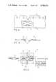
- FIG. 2A carrier element that can be produced very simply by using the intermediate product shown in FIGS. 1a and 1b is shown in FIG. 2.
- the film 3 that is contacted with the semiconductor wafers 1is directed to a casting unit 6.
- the two mold halves 6a and 6bare arranged perpendicularly movable with respect to the film level.
- the casting unitis filled with an appropriate casting material via a feed channel 6c.
- the drain channel 8prevents air pockets from forming in the casting unit during the casting process. Casting arrangements of this sort are known, so that it is not necessary to go into detail here.
- the solidity of the finished carrier elementscan be varied within wide limits by the choice of the casting material.
- the carrier element produced according to the representation in FIG. 2, which can be punched out of the carrier film as a compact unit 10 after the casting process,is suitable, for example, for indirect (contactless) accessing as by capacitive or optical means.
- FIG. 3shows a carrier element which is suitable for direct, galvanic contacting.
- the contact surfaces 4aare initially coated before the casting process, so that bumps 7 are formed over the contact surfaces.
- the coatingcan consist of conductive material, which is, for example, galvanically applied to the contact surfaces.
- the coatingcan also consist of a non-conductive, elastic material (e.g. silicone), which is, for example, applied to the contact surfaces with a wiper by using an appropriate mask.
- a non-conductive, elastic materiale.g. silicone
- the arrangement thus provided with bumps 7is finally directed back into an appropriate casting unit and punched out of the carrier film as a compact unit 11 after the casting process.
- the bumps 7can be formed in such a way that they extend slightly out of the cast block 11. In the case of this carrier element the contact surfaces are then on the same level as the cover film surface of the identification card after the carrier element has been incorporated into the card.
- the carrier elementis suitable for galvanic (direct) contacting.
- the bumpsare formed out of non-conductive material, needles, for example, can be used for contacting, which are directed through the non-conductive material (e.g. silicone) onto the actual contact surfaces 4a.
- non-conductive materiale.g. silicone
- the above-mentioned embodimentsuse for their intermediate products an arrangement in which the semiconductor wafers are connected in a self-supporting way in punched out windows of a film with the appropriate connection leads.
- a disadvantage of this type of arrangementcan result in certain cases of application when as small an interval as possible is required between the contact surfaces.
- the minimal distance of the contact surfacesis determined by the size of the punched out window and thus by the size of the semiconductor wafer.
- the contact surfaces 16 arranged on both sides of the film 12are connected with each other by a throughplating process.
- the semiconductor wafer 1is applied to the film prepared in this way by the known techniques.
- FIGS. 5a, 5bshow the carrier element 15 produced by using the above-mentioned intermediate product in cross-section and from the top.
- the casting processcan be carried out similarly to the manner described in connection with FIG. 2.
- the use of this latter intermediate productallows for a closely adjacent arrangement of the contact surfaces 16.
- FIG. 6shows a carrier element for which a so-called through hole plated film is also used as an intermediate product. This arrangement is characterized by extremely great rigidity.
- the carrier elementconsists in this case of a so-called through hole plated film 12, a spacing film 17 and a rearward cover film 18.
- the rearward cover filmis provided with openings 19 which allow for the inflow and draining of the casting material in the casting unit.
- the spacing film 17has hollows 20 at regular intervals to accept the semiconductor wafers.
- the hollow 20is filled with an appropriate casting material.
- a part of the casting massalso penetrates between the various films, so that the latter are connected with each other particularly well.
- the various films 12, 17, 18are connected with each other in this example by an appropriate adhesive 25. In this way the penetration of the casting mass into the interstices is made easier and simultaneously restricted.
- the restriction of the casting masscan, of course, also be achieved by pressing the film compound together on both sides of the casting unit.
- the rigidity of the arrangementcan be further improved by using films made of epoxy resin reinforced by glass fiber (GEP) and having the resin chosen for the production of the films be identical to the casting mass.
- GEPglass fiber
- the casting massalso penetrates between the various films, which allows for the production of a carrier element with great rigidity and a compact construction.
- FIGS. 7a and 7bshow a further embodiment of an employable intermediate product for the production of carrier elements.
- the semiconductor wafer 30 shown hereis contacted by the so-called bonding technique.
- the carrier film 31is initially punched out at regular intervals in such a way that the recess 32 with its finger-shaped extensions 32a as shown in the figures result.
- the carrier film 31is laminated over its entire surface with a film 33 of conductive material. According to known etching techniques the areas 34 are now isolated from this film, which areas form the contact surfaces of the finished carrier element.
- the carrier film prepared in this manneris finally provided with semiconductor wafers in commercial bonding automata.
- one wafer 30 at a timeis set into the recess 32 and attached to the conductive film 33 by aid of an appropriate adhesive 36.
- the connection points of the wafer 30are connected with the contact surfaces 34 by fine golden wires 37.
- FIG. 8shows the carrier element 40 produced according to FIGS. 7a and 7b, in which the recess 32 with its finger-shaped extensions 32a is filled, for example, with an appropriate resin in a casting unit of the above-mentioned kind.
- the resinalso penetrates into the areas 39 between the contact surfaces 34 that arose during the etching process.
- the filling of the hollowsdoes not necessarily have to be carried out in one of the casting units shown above in the case of the latter arrangement. If the arrangement is sealed on one side, as shown in FIG. 8, for example with a self-adhesive film 38, the hollows can be easily filled with a resin.
- the self-adhesive filmwhich is removed before further processing of the carrier element, simultaneously offers good protection to the contact surfaces, in case the carrier elements are to be stored for long periods.
Landscapes
- Engineering & Computer Science (AREA)
- Microelectronics & Electronic Packaging (AREA)
- Computer Hardware Design (AREA)
- Physics & Mathematics (AREA)
- General Physics & Mathematics (AREA)
- Power Engineering (AREA)
- Condensed Matter Physics & Semiconductors (AREA)
- Theoretical Computer Science (AREA)
- Credit Cards Or The Like (AREA)
- Structures Or Materials For Encapsulating Or Coating Semiconductor Devices Or Solid State Devices (AREA)
- Wire Bonding (AREA)
- Encapsulation Of And Coatings For Semiconductor Or Solid State Devices (AREA)
- Container, Conveyance, Adherence, Positioning, Of Wafer (AREA)
Abstract
Description
Claims (6)
Applications Claiming Priority (2)
| Application Number | Priority Date | Filing Date | Title |
|---|---|---|---|
| DE19803029667DE3029667A1 (en) | 1980-08-05 | 1980-08-05 | CARRIER ELEMENT FOR AN IC COMPONENT |
| DE3029667 | 1981-08-05 |
Related Parent Applications (1)
| Application Number | Title | Priority Date | Filing Date |
|---|---|---|---|
| US06288384Continuation | 1981-07-31 |
Related Child Applications (1)
| Application Number | Title | Priority Date | Filing Date |
|---|---|---|---|
| US07/051,850ContinuationUS4803542A (en) | 1980-08-05 | 1987-05-18 | Carrier element for an IC-module |
Publications (1)
| Publication Number | Publication Date |
|---|---|
| US4709254Atrue US4709254A (en) | 1987-11-24 |
Family
ID=6108951
Family Applications (2)
| Application Number | Title | Priority Date | Filing Date |
|---|---|---|---|
| US06/649,159Expired - LifetimeUS4709254A (en) | 1980-08-05 | 1984-09-10 | Carrier element for an IC module |
| US07/051,850Expired - LifetimeUS4803542A (en) | 1980-08-05 | 1987-05-18 | Carrier element for an IC-module |
Family Applications After (1)
| Application Number | Title | Priority Date | Filing Date |
|---|---|---|---|
| US07/051,850Expired - LifetimeUS4803542A (en) | 1980-08-05 | 1987-05-18 | Carrier element for an IC-module |
Country Status (10)
| Country | Link |
|---|---|
| US (2) | US4709254A (en) |
| JP (2) | JPH0158657B2 (en) |
| BE (1) | BE889815A (en) |
| CH (1) | CH663115A5 (en) |
| DE (2) | DE3029667A1 (en) |
| FR (1) | FR2488446A1 (en) |
| GB (2) | GB2081974B (en) |
| IT (1) | IT1137805B (en) |
| NL (1) | NL194174C (en) |
| SE (1) | SE461694B (en) |
Cited By (20)
| Publication number | Priority date | Publication date | Assignee | Title |
|---|---|---|---|---|
| US4803542A (en)* | 1980-08-05 | 1989-02-07 | Gao Gessellschaft Fur Automation Und Organisation Mbh | Carrier element for an IC-module |
| US4835846A (en)* | 1987-09-14 | 1989-06-06 | Em Microelectronic Marin Sa | Method of manufacture of electronic modules for cards with microcircuits |
| US4961105A (en)* | 1986-02-06 | 1990-10-02 | Hitachi Maxell, Ltd | Arrangement of a semiconductor device for use in a card |
| US5091769A (en)* | 1991-03-27 | 1992-02-25 | Eichelberger Charles W | Configuration for testing and burn-in of integrated circuit chips |
| US5107325A (en)* | 1989-04-17 | 1992-04-21 | Seiko Epson Corporation | Structure and method of packaging a semiconductor device |
| US5182631A (en)* | 1988-04-15 | 1993-01-26 | Nippon Telegraph And Telephone Corporation | Film carrier for RF IC |
| DE4209184C1 (en)* | 1992-03-21 | 1993-05-19 | Orga Kartensysteme Gmbh, 6072 Dreieich, De | |
| US5244840A (en)* | 1989-05-23 | 1993-09-14 | Mitsubishi Denki Kabushiki Kaisha | Method for manufacturing an encapsulated IC card having a molded frame and a circuit board |
| US5278442A (en)* | 1991-07-15 | 1994-01-11 | Prinz Fritz B | Electronic packages and smart structures formed by thermal spray deposition |
| FR2720685A1 (en)* | 1994-05-31 | 1995-12-08 | Seiko Epson Corp | Ink jet recording apparatus. |
| DE19625228A1 (en)* | 1996-06-24 | 1998-01-02 | Siemens Ag | System carrier for mounting an integrated circuit in an injection molded housing |
| US6020627A (en)* | 1996-03-12 | 2000-02-01 | Siemens Aktiengesellschaft | Chip card and method of manufacturing a chip card |
| US6208019B1 (en)* | 1998-03-13 | 2001-03-27 | Kabushiki Kaisha Toshiba | Ultra-thin card-type semiconductor device having an embredded semiconductor element in a space provided therein |
| WO2002063683A2 (en) | 2001-02-09 | 2002-08-15 | Koninklijke Philips Electronics N.V. | Method of manufacturing a semiconductor device and a semiconductor device obtained by means of said method |
| US6572021B1 (en)* | 1998-09-10 | 2003-06-03 | Skidata Ag | Card-shaped data carrier and method for producing the same |
| US6782612B2 (en)* | 2000-08-02 | 2004-08-31 | Wen-Wen Chiu | Manufacturing process of IC module |
| WO2005122072A1 (en)* | 2004-06-09 | 2005-12-22 | Giesecke & Devrient Gmbh | Method for producing a portable data carrier |
| EP1780662A1 (en)* | 2005-10-27 | 2007-05-02 | Axalto SA | Reinforced chipcard module and method of manufacturing the same |
| EP1804202A1 (en)* | 2006-01-02 | 2007-07-04 | Tibc Corporation | Tape carrier and module for contact type IC card and method for manufacturing the tape carrier |
| US20100122457A1 (en)* | 2008-11-19 | 2010-05-20 | Fujitsu Limited | Application method and apparatus for resin |
Families Citing this family (84)
| Publication number | Priority date | Publication date | Assignee | Title |
|---|---|---|---|---|
| US4549247A (en)* | 1980-11-21 | 1985-10-22 | Gao Gesellschaft Fur Automation Und Organisation Mbh | Carrier element for IC-modules |
| DE3131216C3 (en)* | 1981-04-14 | 1994-09-01 | Gao Ges Automation Org | ID card with IC module |
| FR2520541A1 (en)* | 1982-01-22 | 1983-07-29 | Flonic Sa | Mounting assembly for memory integrated circuit in bank card - comprises flexible film support carrying metallic connecting pads for chip connections |
| FR2521350B1 (en)* | 1982-02-05 | 1986-01-24 | Hitachi Ltd | SEMICONDUCTOR CHIP HOLDER |
| DE3235650A1 (en)* | 1982-09-27 | 1984-03-29 | Philips Patentverwaltung Gmbh, 2000 Hamburg | INFORMATION CARD AND METHOD FOR THEIR PRODUCTION |
| CH660551GA3 (en)* | 1982-12-27 | 1987-05-15 | ||
| DE3248385A1 (en)* | 1982-12-28 | 1984-06-28 | GAO Gesellschaft für Automation und Organisation mbH, 8000 München | ID CARD WITH INTEGRATED CIRCUIT |
| US4581678A (en)* | 1983-03-16 | 1986-04-08 | Oxley Developments Company Limited | Circuit component assemblies |
| EP0128822B1 (en)* | 1983-06-09 | 1987-09-09 | Flonic S.A. | Method of producing memory cards, and cards obtained thereby |
| FR2548857B1 (en)* | 1983-07-04 | 1987-11-27 | Cortaillod Cables Sa | PROCESS FOR THE CONTINUOUS MANUFACTURE OF A PRINTED CARD |
| DE3338597A1 (en)* | 1983-10-24 | 1985-05-02 | GAO Gesellschaft für Automation und Organisation mbH, 8000 München | DATA CARRIER WITH INTEGRATED CIRCUIT AND METHOD FOR PRODUCING THE SAME |
| JPS6180195U (en)* | 1984-11-01 | 1986-05-28 | ||
| JPS61123990A (en)* | 1984-11-05 | 1986-06-11 | Casio Comput Co Ltd | Ic card |
| FR2579798B1 (en)* | 1985-04-02 | 1990-09-28 | Ebauchesfabrik Eta Ag | METHOD FOR MANUFACTURING ELECTRONIC MODULES FOR MICROCIRCUIT CARDS AND MODULES OBTAINED ACCORDING TO THIS METHOD |
| FR2580416B1 (en)* | 1985-04-12 | 1987-06-05 | Radiotechnique Compelec | METHOD AND DEVICE FOR MANUFACTURING AN ELECTRONIC IDENTIFICATION CARD |
| FR2583574B1 (en)* | 1985-06-14 | 1988-06-17 | Eurotechnique Sa | MICROMODULE WITH BURIAL CONTACTS AND CARD CONTAINING CIRCUITS COMPRISING SUCH A MICROMODULE. |
| FR2584862B1 (en)* | 1985-07-12 | 1988-05-20 | Eurotechnique Sa | PROCESS FOR THE CONTINUOUS MANUFACTURE OF MICROMODULES FOR CARDS CONTAINING COMPONENTS, CONTINUOUS BAND OF MICROMODULES AND MICROMODULES CARRIED OUT BY SUCH A PROCESS |
| DE3689147T2 (en)* | 1985-07-17 | 1994-03-24 | Ibiden Co Ltd | A method of manufacturing a printed circuit board for semiconductor circuits. |
| FR2588695B1 (en)* | 1985-10-11 | 1988-07-29 | Eurotechnique Sa | PROCESS FOR THE MANUFACTURE OF A MICROBOX, MICROBOX WITH TOUCHING CONTACTS AND APPLICATION TO CARDS CONTAINING COMPONENTS |
| FR2590052B1 (en)* | 1985-11-08 | 1991-03-01 | Eurotechnique Sa | METHOD FOR RECYCLING A CARD COMPRISING A COMPONENT, CARD PROVIDED FOR RECYCLE |
| FR2590051B1 (en)* | 1985-11-08 | 1991-05-17 | Eurotechnique Sa | CARD COMPRISING A COMPONENT AND MICROMODULE WITH SIDING CONTACTS |
| DE3624852A1 (en)* | 1986-01-10 | 1987-07-16 | Orga Druck Gmbh | Electronic data and/or programme carriers and production method therefor |
| JPS62161595A (en)* | 1986-01-13 | 1987-07-17 | 日立マクセル株式会社 | Manufacture of integrated circuit card |
| JPS6314455A (en)* | 1986-07-07 | 1988-01-21 | Hitachi Maxell Ltd | semiconductor equipment |
| JPH0524554Y2 (en)* | 1986-07-21 | 1993-06-22 | ||
| FR2609821B1 (en)* | 1987-01-16 | 1989-03-31 | Flonic Sa | METHOD FOR REALIZING MEMORY CARDS AND CARDS OBTAINED BY THE IMPLEMENTATION OF SAID METHOD |
| AU8034087A (en)* | 1987-02-20 | 1988-09-14 | Lsi Logic Corporation | Integrated circuit package assembly |
| US4907060A (en)* | 1987-06-02 | 1990-03-06 | Nelson John L | Encapsulated thermoelectric heat pump and method of manufacture |
| FR2617668B1 (en)* | 1987-07-03 | 1995-07-07 | Radiotechnique Compelec | DEVICE COMPRISING AN ELECTRONIC CIRCUIT MOUNTED ON A FLEXIBLE SUPPORT AND FLEXIBLE CARD INCLUDING THE SAME |
| FR2624652B1 (en)* | 1987-12-14 | 1990-08-31 | Sgs Thomson Microelectronics | METHOD OF PLACING ON AN SUPPORT, AN ELECTRONIC COMPONENT PROVIDED WITH ITS CONTACTS |
| FR2630843B1 (en)* | 1988-04-28 | 1990-08-03 | Schlumberger Ind Sa | PROCESS FOR PRODUCING CARDS COMPRISING GRAPHIC ELEMENTS AND CARDS OBTAINED BY SAID METHOD |
| US5030407A (en)* | 1988-04-28 | 1991-07-09 | Schlumberger Industries | Method of making cards having graphics elements thereon |
| DE68912426T2 (en)* | 1988-06-21 | 1994-05-11 | Gec Avery Ltd | Manufacture of portable electronic cards. |
| US5387306A (en)* | 1988-06-21 | 1995-02-07 | Gec Avery Limited | Manufacturing integrated circuit cards |
| USRE35578E (en)* | 1988-12-12 | 1997-08-12 | Sgs-Thomson Microelectronics, Inc. | Method to install an electronic component and its electrical connections on a support, and product obtained thereby |
| FR2641102B1 (en)* | 1988-12-27 | 1991-02-22 | Ebauchesfabrik Eta Ag | |
| DE3905657A1 (en)* | 1989-02-24 | 1990-08-30 | Telefunken Electronic Gmbh | Flexible supporting film |
| DE3912891A1 (en)* | 1989-04-19 | 1990-11-08 | Siemens Ag | MOUNTING DEVICE FOR CONTACTING AND INSTALLING AN INTEGRATED CIRCUIT SYSTEM FOR A VALUE CARD |
| DE3924439A1 (en)* | 1989-07-24 | 1991-04-18 | Edgar Schneider | CARRIER ELEMENT WITH AT LEAST ONE INTEGRATED CIRCUIT, ESPECIALLY FOR INSTALLATION IN CHIP CARDS, AND METHOD FOR THE PRODUCTION OF THESE CARRIER ELEMENTS |
| JPH0680706B2 (en)* | 1989-08-22 | 1994-10-12 | 三菱電機株式会社 | Carrier tape and method of manufacturing semiconductor device using the same |
| US5155068A (en)* | 1989-08-31 | 1992-10-13 | Sharp Kabushiki Kaisha | Method for manufacturing an IC module for an IC card whereby an IC device and surrounding encapsulant are thinned by material removal |
| DE9100665U1 (en)* | 1991-01-21 | 1992-07-16 | TELBUS Gesellschaft für elektronische Kommunikations-Systeme mbH, 85391 Allershausen | Carrier element for integrated semiconductor circuits, especially for installation in chip cards |
| ATE133105T1 (en)* | 1991-05-10 | 1996-02-15 | Gao Ges Automation Org | METHOD AND DEVICE FOR PRODUCING PLASTIC MOLDINGS WITH PARTIALLY REDUCED WALL THICKNESS |
| EP0553477A2 (en)* | 1992-01-30 | 1993-08-04 | Siemens Aktiengesellschaft | Printed circuit board to be equipped with components |
| DE4224103A1 (en)* | 1992-07-22 | 1994-01-27 | Manfred Dr Ing Michalk | Miniature housing with electronic components |
| JP2774906B2 (en)* | 1992-09-17 | 1998-07-09 | 三菱電機株式会社 | Thin semiconductor device and method of manufacturing the same |
| DE4232625A1 (en)* | 1992-09-29 | 1994-03-31 | Siemens Ag | Method of assembling integrated semiconductor circuits |
| CH686325A5 (en)* | 1992-11-27 | 1996-02-29 | Esec Sempac Sa | Electronic module and chip card. |
| ZA941671B (en)* | 1993-03-11 | 1994-10-12 | Csir | Attaching an electronic circuit to a substrate. |
| GB9313749D0 (en)* | 1993-07-02 | 1993-08-18 | Gec Avery Ltd | A device comprising a flexible printed circuit |
| EP0644587B1 (en)* | 1993-09-01 | 2002-07-24 | Kabushiki Kaisha Toshiba | Semiconductor package and fabrication method |
| DE4336501A1 (en)* | 1993-10-26 | 1995-04-27 | Giesecke & Devrient Gmbh | Process for the production of identity cards with electronic modules |
| DE4337921C2 (en)* | 1993-11-06 | 1998-09-03 | Ods Gmbh & Co Kg | Contactless chip card with antenna coil |
| DE4340847A1 (en)* | 1993-11-26 | 1995-06-01 | Optosys Gmbh Berlin | Chip module with chip on substrate material |
| DE4401588C2 (en)* | 1994-01-20 | 2003-02-20 | Gemplus Gmbh | Method for capping a chip card module and chip card module |
| FR2715754B1 (en)* | 1994-02-01 | 1996-03-29 | Gemplus Card Int | Method for protecting the contact pads of a memory card. |
| WO1995032520A1 (en)* | 1994-05-23 | 1995-11-30 | Toray Industries, Inc. | Electronic device package and its manufacture |
| FR2721731B1 (en)* | 1994-06-24 | 1996-08-09 | Schlumberger Ind Sa | Memory card. |
| DE4427309C2 (en)* | 1994-08-02 | 1999-12-02 | Ibm | Production of a carrier element module for installation in chip cards or other data carrier cards |
| DE19512191C2 (en)* | 1995-03-31 | 2000-03-09 | Siemens Ag | Card-shaped data carrier and lead frame for use in such a data carrier |
| DE19526010B4 (en)* | 1995-07-17 | 2005-10-13 | Infineon Technologies Ag | Electronic component |
| FR2738077B1 (en)* | 1995-08-23 | 1997-09-19 | Schlumberger Ind Sa | ELECTRONIC MICRO-BOX FOR ELECTRONIC MEMORY CARD AND EMBODIMENT PROCESS |
| US5817207A (en) | 1995-10-17 | 1998-10-06 | Leighton; Keith R. | Radio frequency identification card and hot lamination process for the manufacture of radio frequency identification cards |
| DE19539181C2 (en)* | 1995-10-20 | 1998-05-14 | Ods Gmbh & Co Kg | Chip card module and corresponding manufacturing process |
| RU2173476C2 (en)* | 1995-11-03 | 2001-09-10 | Сименс Акциенгезелльшафт | Integrated circuit module |
| DE19541072A1 (en)* | 1995-11-03 | 1997-05-07 | Siemens Ag | Chip module |
| US5786988A (en)* | 1996-07-02 | 1998-07-28 | Sandisk Corporation | Integrated circuit chips made bendable by forming indentations in their back surfaces flexible packages thereof and methods of manufacture |
| DE19705615A1 (en)* | 1997-02-14 | 1998-06-04 | Dirk Prof Dr Ing Jansen | Chip-card for measuring and displaying temperature e.g. for monitoring foodstuffs cooling chain during transportation |
| DE19708617C2 (en) | 1997-03-03 | 1999-02-04 | Siemens Ag | Chip card module and method for its production as well as this comprehensive chip card |
| DE19845665C2 (en)* | 1998-10-05 | 2000-08-17 | Orga Kartensysteme Gmbh | Method for producing a carrier element for an IC chip for installation in chip cards |
| FR2788882A1 (en)* | 1999-01-27 | 2000-07-28 | Schlumberger Systems & Service | Integrated circuit module for smart card |
| MX2009007905A (en)* | 2007-02-09 | 2009-07-31 | Nagraid Sa | Method for producing electronic cards including at least one printed pattern. |
| US8649820B2 (en) | 2011-11-07 | 2014-02-11 | Blackberry Limited | Universal integrated circuit card apparatus and related methods |
| US8936199B2 (en) | 2012-04-13 | 2015-01-20 | Blackberry Limited | UICC apparatus and related methods |
| USD703208S1 (en) | 2012-04-13 | 2014-04-22 | Blackberry Limited | UICC apparatus |
| USD701864S1 (en) | 2012-04-23 | 2014-04-01 | Blackberry Limited | UICC apparatus |
| USD707682S1 (en)* | 2012-12-05 | 2014-06-24 | Logomotion, S.R.O. | Memory card |
| US9888283B2 (en) | 2013-03-13 | 2018-02-06 | Nagrastar Llc | Systems and methods for performing transport I/O |
| US9647997B2 (en) | 2013-03-13 | 2017-05-09 | Nagrastar, Llc | USB interface for performing transport I/O |
| USD759022S1 (en) | 2013-03-13 | 2016-06-14 | Nagrastar Llc | Smart card interface |
| USD758372S1 (en) | 2013-03-13 | 2016-06-07 | Nagrastar Llc | Smart card interface |
| USD729808S1 (en)* | 2013-03-13 | 2015-05-19 | Nagrastar Llc | Smart card interface |
| USD780763S1 (en)* | 2015-03-20 | 2017-03-07 | Nagrastar Llc | Smart card interface |
| USD864968S1 (en) | 2015-04-30 | 2019-10-29 | Echostar Technologies L.L.C. | Smart card interface |
Citations (11)
| Publication number | Priority date | Publication date | Assignee | Title |
|---|---|---|---|---|
| US3558993A (en)* | 1967-09-01 | 1971-01-26 | Lucas Industries Ltd | Electrical component assemblies with improved printed circuit construction |
| US3591839A (en)* | 1969-08-27 | 1971-07-06 | Siliconix Inc | Micro-electronic circuit with novel hermetic sealing structure and method of manufacture |
| US3611065A (en)* | 1968-09-30 | 1971-10-05 | Siemens Ag | Carrier for semiconductor components |
| US3706464A (en)* | 1970-12-13 | 1972-12-19 | Canadian Kenworth Ltd | Power system for loading an empty trailer onto a tractor or for loading pre-loaded trailers onto a fifth wheel of the tractor |
| US3864728A (en)* | 1970-11-20 | 1975-02-04 | Siemens Ag | Semiconductor components having bimetallic lead connected thereto |
| US3868724A (en)* | 1973-11-21 | 1975-02-25 | Fairchild Camera Instr Co | Multi-layer connecting structures for packaging semiconductor devices mounted on a flexible carrier |
| US4143456A (en)* | 1976-06-28 | 1979-03-13 | Citizen Watch Commpany Ltd. | Semiconductor device insulation method |
| US4222516A (en)* | 1975-12-31 | 1980-09-16 | Compagnie Internationale Pour L'informatique Cii-Honeywell Bull | Standardized information card |
| US4264917A (en)* | 1978-10-19 | 1981-04-28 | Compagnie Internationale Pour L'informatique Cii-Honeywell Bull | Flat package for integrated circuit devices |
| US4300153A (en)* | 1977-09-22 | 1981-11-10 | Sharp Kabushiki Kaisha | Flat shaped semiconductor encapsulation |
| US4336551A (en)* | 1977-05-30 | 1982-06-22 | Hitachi, Ltd. | Thick-film printed circuit board and method for producing the same |
Family Cites Families (31)
| Publication number | Priority date | Publication date | Assignee | Title |
|---|---|---|---|---|
| DE1915501U (en) | 1964-04-11 | 1965-05-13 | Fritsch K G A | HOERNCHEN WRAPPING DEVICE FOR Dough sheeting machines. |
| DE1909480U (en) | 1964-12-07 | 1965-02-04 | Fritz Krug | DEVICE FOR GRINDING SAW CHAINS. |
| GB1249360A (en)* | 1967-12-30 | 1971-10-13 | Sony Corp | Lead assembly and method of making the same |
| DE1909480C2 (en)* | 1968-03-01 | 1984-10-11 | General Electric Co., Schenectady, N.Y. | Carrier arrangement and method for the electrical contacting of semiconductor chips |
| US3570115A (en)* | 1968-05-06 | 1971-03-16 | Honeywell Inc | Method for mounting electronic chips |
| DE1915501C3 (en)* | 1969-03-26 | 1975-10-16 | Siemens Ag, 1000 Berlin Und 8000 Muenchen | Method for connecting an integrated circuit to external electrical leads |
| US3848077A (en)* | 1970-10-16 | 1974-11-12 | M Whitman | Package for electronic semiconductor devices |
| JPS5247419Y2 (en)* | 1972-10-09 | 1977-10-27 | ||
| JPS5040166U (en)* | 1973-08-10 | 1975-04-24 | ||
| JPS5853874B2 (en)* | 1973-09-03 | 1983-12-01 | アリムラ クニタカ | Atsuden on Kansoshio Mochiita Kenshiyutsuhouhou |
| DE2414297C3 (en)* | 1974-03-25 | 1980-01-17 | Siemens Ag, 1000 Berlin Und 8000 Muenchen | Process for the semi-automatic production of intermediate carriers for semiconductor components |
| JPS5716386Y2 (en)* | 1974-04-18 | 1982-04-06 | ||
| JPS519578A (en)* | 1974-07-12 | 1976-01-26 | Sharp Kk | Handotaisochino seizoho |
| US4004133A (en)* | 1974-12-30 | 1977-01-18 | Rca Corporation | Credit card containing electronic circuit |
| FR2299724A1 (en)* | 1975-01-29 | 1976-08-27 | Honeywell Bull Soc Ind | IMPROVEMENTS TO PACKAGING MEDIA FOR INTEGRATED CIRCUIT BOARDS |
| JPS51130866A (en)* | 1975-05-08 | 1976-11-13 | Seiko Instr & Electronics | Method of mounting electronic timekeeper circuits |
| FR2337381A1 (en)* | 1975-12-31 | 1977-07-29 | Honeywell Bull Soc Ind | PORTABLE CARD FOR ELECTRICAL SIGNAL PROCESSING SYSTEM AND PROCESS FOR MANUFACTURING THIS CARD |
| US4064552A (en)* | 1976-02-03 | 1977-12-20 | Angelucci Thomas L | Multilayer flexible printed circuit tape |
| JPS591463B2 (en)* | 1976-07-01 | 1984-01-12 | 鐘淵化学工業株式会社 | Foaming composition |
| JPS535571A (en)* | 1976-07-05 | 1978-01-19 | Seiko Instr & Electronics Ltd | Circuit block and its manufacture |
| JPS5923110B2 (en)* | 1976-11-09 | 1984-05-30 | 松下電器産業株式会社 | Film carrier type electronic component mounting device |
| JPS5481073A (en)* | 1977-12-12 | 1979-06-28 | Seiko Instr & Electronics Ltd | Sealing method for semiconductor element |
| JPS5513985A (en)* | 1978-07-18 | 1980-01-31 | Citizen Watch Co Ltd | Ic mounting structure |
| FR2439438A1 (en)* | 1978-10-19 | 1980-05-16 | Cii Honeywell Bull | RIBBON CARRYING ELECTRIC SIGNAL PROCESSING DEVICES, MANUFACTURING METHOD THEREOF AND APPLICATION THEREOF TO A SIGNAL PROCESSING ELEMENT |
| JPS5562591A (en)* | 1978-10-30 | 1980-05-12 | Fujitsu Ltd | Memory card |
| DE2920012C2 (en) | 1979-05-17 | 1988-09-29 | GAO Gesellschaft für Automation und Organisation mbH, 8000 München | Identification card with IC component and method for producing such an identification card |
| FR2480008A1 (en)* | 1980-04-04 | 1981-10-09 | Flonic Sa | IMPROVEMENTS TO MEMORY CARDS |
| DE3019207A1 (en)* | 1980-05-20 | 1981-11-26 | GAO Gesellschaft für Automation und Organisation mbH, 8000 München | CARRIER ELEMENT FOR AN IC CHIP |
| DE3029667A1 (en)* | 1980-08-05 | 1982-03-11 | GAO Gesellschaft für Automation und Organisation mbH, 8000 München | CARRIER ELEMENT FOR AN IC COMPONENT |
| JPS6018145B2 (en)* | 1980-09-22 | 1985-05-09 | 株式会社日立製作所 | Resin-encapsulated semiconductor device |
| GB2093401B (en)* | 1981-01-17 | 1985-07-17 | Sanyo Electric Co | Composite film |
- 1980
- 1980-08-05DEDE19803029667patent/DE3029667A1/enactiveGranted
- 1980-08-05DEDE19803051195patent/DE3051195C2/ennot_activeExpired - Lifetime
- 1981
- 1981-07-30NLNL8103598Apatent/NL194174C/ennot_activeIP Right Cessation
- 1981-07-31BEBE0/205546Apatent/BE889815A/ennot_activeIP Right Cessation
- 1981-08-03CHCH4999/81Apatent/CH663115A5/ennot_activeIP Right Cessation
- 1981-08-04SESE8104663Apatent/SE461694B/ennot_activeIP Right Cessation
- 1981-08-04ITIT2337281Apatent/IT1137805B/enactive
- 1981-08-04FRFR8115130Apatent/FR2488446A1/enactiveGranted
- 1981-08-05GBGB8123900Apatent/GB2081974B/ennot_activeExpired
- 1981-08-05JPJP56121982Apatent/JPH0158657B2/janot_activeExpired
- 1984
- 1984-09-10USUS06/649,159patent/US4709254A/ennot_activeExpired - Lifetime
- 1984-12-13GBGB8431488Apatent/GB2149209B/ennot_activeExpired
- 1987
- 1987-05-18USUS07/051,850patent/US4803542A/ennot_activeExpired - Lifetime
- 1991
- 1991-10-09JPJP26244391Apatent/JP2702012B2/ennot_activeExpired - Lifetime
Patent Citations (11)
| Publication number | Priority date | Publication date | Assignee | Title |
|---|---|---|---|---|
| US3558993A (en)* | 1967-09-01 | 1971-01-26 | Lucas Industries Ltd | Electrical component assemblies with improved printed circuit construction |
| US3611065A (en)* | 1968-09-30 | 1971-10-05 | Siemens Ag | Carrier for semiconductor components |
| US3591839A (en)* | 1969-08-27 | 1971-07-06 | Siliconix Inc | Micro-electronic circuit with novel hermetic sealing structure and method of manufacture |
| US3864728A (en)* | 1970-11-20 | 1975-02-04 | Siemens Ag | Semiconductor components having bimetallic lead connected thereto |
| US3706464A (en)* | 1970-12-13 | 1972-12-19 | Canadian Kenworth Ltd | Power system for loading an empty trailer onto a tractor or for loading pre-loaded trailers onto a fifth wheel of the tractor |
| US3868724A (en)* | 1973-11-21 | 1975-02-25 | Fairchild Camera Instr Co | Multi-layer connecting structures for packaging semiconductor devices mounted on a flexible carrier |
| US4222516A (en)* | 1975-12-31 | 1980-09-16 | Compagnie Internationale Pour L'informatique Cii-Honeywell Bull | Standardized information card |
| US4143456A (en)* | 1976-06-28 | 1979-03-13 | Citizen Watch Commpany Ltd. | Semiconductor device insulation method |
| US4336551A (en)* | 1977-05-30 | 1982-06-22 | Hitachi, Ltd. | Thick-film printed circuit board and method for producing the same |
| US4300153A (en)* | 1977-09-22 | 1981-11-10 | Sharp Kabushiki Kaisha | Flat shaped semiconductor encapsulation |
| US4264917A (en)* | 1978-10-19 | 1981-04-28 | Compagnie Internationale Pour L'informatique Cii-Honeywell Bull | Flat package for integrated circuit devices |
Cited By (30)
| Publication number | Priority date | Publication date | Assignee | Title |
|---|---|---|---|---|
| US4803542A (en)* | 1980-08-05 | 1989-02-07 | Gao Gessellschaft Fur Automation Und Organisation Mbh | Carrier element for an IC-module |
| US4961105A (en)* | 1986-02-06 | 1990-10-02 | Hitachi Maxell, Ltd | Arrangement of a semiconductor device for use in a card |
| US4835846A (en)* | 1987-09-14 | 1989-06-06 | Em Microelectronic Marin Sa | Method of manufacture of electronic modules for cards with microcircuits |
| US5182631A (en)* | 1988-04-15 | 1993-01-26 | Nippon Telegraph And Telephone Corporation | Film carrier for RF IC |
| US5107325A (en)* | 1989-04-17 | 1992-04-21 | Seiko Epson Corporation | Structure and method of packaging a semiconductor device |
| US5244840A (en)* | 1989-05-23 | 1993-09-14 | Mitsubishi Denki Kabushiki Kaisha | Method for manufacturing an encapsulated IC card having a molded frame and a circuit board |
| US5091769A (en)* | 1991-03-27 | 1992-02-25 | Eichelberger Charles W | Configuration for testing and burn-in of integrated circuit chips |
| US5278442A (en)* | 1991-07-15 | 1994-01-11 | Prinz Fritz B | Electronic packages and smart structures formed by thermal spray deposition |
| DE4209184C1 (en)* | 1992-03-21 | 1993-05-19 | Orga Kartensysteme Gmbh, 6072 Dreieich, De | |
| FR2720685A1 (en)* | 1994-05-31 | 1995-12-08 | Seiko Epson Corp | Ink jet recording apparatus. |
| US5828389A (en)* | 1994-05-31 | 1998-10-27 | Seiko Epson Corporation | Ink jet recording apparatus with selective suction method depending upon ink cartridge replacement |
| US6020627A (en)* | 1996-03-12 | 2000-02-01 | Siemens Aktiengesellschaft | Chip card and method of manufacturing a chip card |
| CN1099703C (en)* | 1996-06-24 | 2003-01-22 | 西门子公司 | Leadframe for the assembly of an integrated circuit in an injection mounded housing |
| DE19625228A1 (en)* | 1996-06-24 | 1998-01-02 | Siemens Ag | System carrier for mounting an integrated circuit in an injection molded housing |
| DE19625228C2 (en)* | 1996-06-24 | 1998-05-14 | Siemens Ag | System carrier for mounting an integrated circuit in an injection molded housing |
| US6614100B1 (en) | 1996-06-24 | 2003-09-02 | Infineon Technologies Ag | Lead frame for the installation of an integrated circuit in an injection-molded package |
| US6208019B1 (en)* | 1998-03-13 | 2001-03-27 | Kabushiki Kaisha Toshiba | Ultra-thin card-type semiconductor device having an embredded semiconductor element in a space provided therein |
| US6572021B1 (en)* | 1998-09-10 | 2003-06-03 | Skidata Ag | Card-shaped data carrier and method for producing the same |
| US6782612B2 (en)* | 2000-08-02 | 2004-08-31 | Wen-Wen Chiu | Manufacturing process of IC module |
| WO2002063683A2 (en) | 2001-02-09 | 2002-08-15 | Koninklijke Philips Electronics N.V. | Method of manufacturing a semiconductor device and a semiconductor device obtained by means of said method |
| WO2002063683A3 (en)* | 2001-02-09 | 2002-10-10 | Koninkl Philips Electronics Nv | Method of manufacturing a semiconductor device and a semiconductor device obtained by means of said method |
| CN1989511B (en)* | 2004-06-09 | 2010-10-06 | 德国捷德有限公司 | Method for producing a portable data carrier |
| WO2005122072A1 (en)* | 2004-06-09 | 2005-12-22 | Giesecke & Devrient Gmbh | Method for producing a portable data carrier |
| US20080135625A1 (en)* | 2004-06-09 | 2008-06-12 | Volker Waschk | Method for Producing a Portable Data Carrier |
| RU2382412C2 (en)* | 2004-06-09 | 2010-02-20 | Гизеке Унд Девриент Гмбх | Method of making portable data carrier |
| US8087591B2 (en) | 2004-06-09 | 2012-01-03 | Giesecke & Devrient Gmbh | Method for producing a portable data carrier |
| EP1780662A1 (en)* | 2005-10-27 | 2007-05-02 | Axalto SA | Reinforced chipcard module and method of manufacturing the same |
| EP1804202A1 (en)* | 2006-01-02 | 2007-07-04 | Tibc Corporation | Tape carrier and module for contact type IC card and method for manufacturing the tape carrier |
| US8065793B2 (en)* | 2008-11-19 | 2011-11-29 | Fujitsu Limited | Method of encapsulating an electronic component |
| US20100122457A1 (en)* | 2008-11-19 | 2010-05-20 | Fujitsu Limited | Application method and apparatus for resin |
Also Published As
| Publication number | Publication date |
|---|---|
| SE461694B (en) | 1990-03-12 |
| JPH0158657B2 (en) | 1989-12-13 |
| GB2149209A (en) | 1985-06-05 |
| GB2149209B (en) | 1985-12-04 |
| IT8123372A0 (en) | 1981-08-04 |
| BE889815A (en) | 1981-11-16 |
| JPS5754356A (en) | 1982-03-31 |
| FR2488446B1 (en) | 1984-11-16 |
| GB2081974A (en) | 1982-02-24 |
| GB2081974B (en) | 1985-07-17 |
| NL8103598A (en) | 1982-03-01 |
| JP2702012B2 (en) | 1998-01-21 |
| FR2488446A1 (en) | 1982-02-12 |
| JPH05270183A (en) | 1993-10-19 |
| NL194174C (en) | 2001-08-03 |
| DE3051195C2 (en) | 1997-08-28 |
| US4803542A (en) | 1989-02-07 |
| DE3029667C2 (en) | 1990-10-11 |
| CH663115A5 (en) | 1987-11-13 |
| DE3029667A1 (en) | 1982-03-11 |
| IT1137805B (en) | 1986-09-10 |
| SE8104663L (en) | 1982-02-06 |
| NL194174B (en) | 2001-04-02 |
| GB8431488D0 (en) | 1985-01-23 |
Similar Documents
| Publication | Publication Date | Title |
|---|---|---|
| US4709254A (en) | Carrier element for an IC module | |
| US4829666A (en) | Method for producing a carrier element for an IC-chip | |
| US4910582A (en) | Semiconductor device and method of manufacturing thereof | |
| US5005282A (en) | Method of making an electronic memory card | |
| US5637536A (en) | Method for interconnecting semiconductor chips in three dimensions, and component resulting therefrom | |
| US4943464A (en) | Electronic component support for memory card and product obtained thereby | |
| KR100358578B1 (en) | Manufacturing process of chip card module, chip card module manufactured by the process and combined chip card containing the module | |
| KR910002035B1 (en) | Semiconductor device and its manufacturing method | |
| USRE35109E (en) | Semiconductor device and method for fabricating the same | |
| US5147982A (en) | Encapsulation of electronic modules | |
| US4483067A (en) | Method of manufacturing an identification card and an identification manufactured, for example, by this method | |
| EP0058068B1 (en) | Integrated circuit chip carrier | |
| US6420790B1 (en) | Semiconductor device | |
| US4526859A (en) | Metallization of a ceramic substrate | |
| US6479887B1 (en) | Circuit pattern tape for wafer-scale production of chip size semiconductor packages | |
| US5124783A (en) | Semiconductor device having insulating substrate adhered to conductive substrate | |
| KR960012397A (en) | Manufacturing method of chip size package type semiconductor device | |
| KR20090079924A (en) | Edge-Connected Wafer Level Stacking | |
| US7163613B2 (en) | Method of manufacturing a semiconductor device by forming plating layers having differing thicknesses | |
| KR890005830A (en) | Semiconductor device and manufacturing method thereof | |
| JPH06244360A (en) | Semiconductor device | |
| USRE36356E (en) | Electronic component support for memory card and product obtained thereby | |
| JPH06227189A (en) | Production of ic card module | |
| EP0186818A2 (en) | Chip to pin interconnect method | |
| JP3394696B2 (en) | Semiconductor device and manufacturing method thereof |
Legal Events
| Date | Code | Title | Description |
|---|---|---|---|
| AS | Assignment | Owner name:GAO GESELLSCHAFT FUR AUTOMATION UND ORGANISATION M Free format text:ASSIGNMENT OF ASSIGNORS INTEREST.;ASSIGNORS:HAGHIRI-TEHRANI, YAHYA;HOPPE, JOACHIM;REEL/FRAME:004681/0610 Effective date:19870120 | |
| STCF | Information on status: patent grant | Free format text:PATENTED CASE | |
| FEPP | Fee payment procedure | Free format text:PAYOR NUMBER ASSIGNED (ORIGINAL EVENT CODE: ASPN); ENTITY STATUS OF PATENT OWNER: LARGE ENTITY | |
| FPAY | Fee payment | Year of fee payment:4 | |
| FEPP | Fee payment procedure | Free format text:PAYER NUMBER DE-ASSIGNED (ORIGINAL EVENT CODE: RMPN); ENTITY STATUS OF PATENT OWNER: LARGE ENTITY Free format text:PAYOR NUMBER ASSIGNED (ORIGINAL EVENT CODE: ASPN); ENTITY STATUS OF PATENT OWNER: LARGE ENTITY | |
| FEPP | Fee payment procedure | Free format text:PAYER NUMBER DE-ASSIGNED (ORIGINAL EVENT CODE: RMPN); ENTITY STATUS OF PATENT OWNER: LARGE ENTITY Free format text:PAYOR NUMBER ASSIGNED (ORIGINAL EVENT CODE: ASPN); ENTITY STATUS OF PATENT OWNER: LARGE ENTITY | |
| FPAY | Fee payment | Year of fee payment:8 | |
| FPAY | Fee payment | Year of fee payment:12 |