US4705606A - Thin-film electrical connections for integrated circuits - Google Patents
Thin-film electrical connections for integrated circuitsDownload PDFInfo
- Publication number
- US4705606A US4705606AUS06/697,092US69709285AUS4705606AUS 4705606 AUS4705606 AUS 4705606AUS 69709285 AUS69709285 AUS 69709285AUS 4705606 AUS4705606 AUS 4705606A
- Authority
- US
- United States
- Prior art keywords
- interconnect lines
- thin
- dielectric layer
- pattern
- film
- Prior art date
- Legal status (The legal status is an assumption and is not a legal conclusion. Google has not performed a legal analysis and makes no representation as to the accuracy of the status listed.)
- Expired - Lifetime
Links
- 239000010409thin filmSubstances0.000titleclaimsabstractdescription54
- 238000000034methodMethods0.000claimsabstractdescription56
- 229910052751metalInorganic materials0.000claimsabstractdescription28
- 239000002184metalSubstances0.000claimsabstractdescription28
- 239000000758substrateSubstances0.000claimsabstractdescription21
- 239000004065semiconductorSubstances0.000claimsabstractdescription13
- 239000004642PolyimideSubstances0.000claimsdescription29
- 229920001721polyimidePolymers0.000claimsdescription29
- 238000004519manufacturing processMethods0.000claimsdescription18
- 238000009713electroplatingMethods0.000claimsdescription14
- 239000000463materialSubstances0.000claimsdescription10
- 238000005530etchingMethods0.000claimsdescription6
- 238000001020plasma etchingMethods0.000claimsdescription3
- 239000010408filmSubstances0.000claims3
- 239000003960organic solventSubstances0.000claims1
- 235000012431wafersNutrition0.000description17
- 239000002243precursorSubstances0.000description13
- 239000004020conductorSubstances0.000description9
- 238000005516engineering processMethods0.000description7
- MHAJPDPJQMAIIY-UHFFFAOYSA-NHydrogen peroxideChemical compoundOOMHAJPDPJQMAIIY-UHFFFAOYSA-N0.000description4
- VYPSYNLAJGMNEJ-UHFFFAOYSA-NSilicium dioxideChemical compoundO=[Si]=OVYPSYNLAJGMNEJ-UHFFFAOYSA-N0.000description4
- 238000004140cleaningMethods0.000description4
- 238000001465metallisationMethods0.000description4
- 229920002120photoresistant polymerPolymers0.000description4
- 229920000642polymerPolymers0.000description4
- VYZAMTAEIAYCRO-UHFFFAOYSA-NChromiumChemical compound[Cr]VYZAMTAEIAYCRO-UHFFFAOYSA-N0.000description3
- XUIMIQQOPSSXEZ-UHFFFAOYSA-NSiliconChemical compound[Si]XUIMIQQOPSSXEZ-UHFFFAOYSA-N0.000description3
- 229910052804chromiumInorganic materials0.000description3
- 239000011651chromiumSubstances0.000description3
- 238000004806packaging method and processMethods0.000description3
- 229910052710siliconInorganic materials0.000description3
- 239000010703siliconSubstances0.000description3
- XLYOFNOQVPJJNP-UHFFFAOYSA-NwaterSubstancesOXLYOFNOQVPJJNP-UHFFFAOYSA-N0.000description3
- XKRFYHLGVUSROY-UHFFFAOYSA-NArgonChemical compound[Ar]XKRFYHLGVUSROY-UHFFFAOYSA-N0.000description2
- IJGRMHOSHXDMSA-UHFFFAOYSA-NAtomic nitrogenChemical compoundN#NIJGRMHOSHXDMSA-UHFFFAOYSA-N0.000description2
- QAOWNCQODCNURD-UHFFFAOYSA-NSulfuric acidChemical compoundOS(O)(=O)=OQAOWNCQODCNURD-UHFFFAOYSA-N0.000description2
- 229910052782aluminiumInorganic materials0.000description2
- XAGFODPZIPBFFR-UHFFFAOYSA-NaluminiumChemical compound[Al]XAGFODPZIPBFFR-UHFFFAOYSA-N0.000description2
- QVGXLLKOCUKJST-UHFFFAOYSA-Natomic oxygenChemical compound[O]QVGXLLKOCUKJST-UHFFFAOYSA-N0.000description2
- 238000009835boilingMethods0.000description2
- 239000008367deionised waterSubstances0.000description2
- 229910021641deionized waterInorganic materials0.000description2
- 238000007598dipping methodMethods0.000description2
- 230000000694effectsEffects0.000description2
- 238000007772electroless platingMethods0.000description2
- PCHJSUWPFVWCPO-UHFFFAOYSA-NgoldChemical compound[Au]PCHJSUWPFVWCPO-UHFFFAOYSA-N0.000description2
- 229910052737goldInorganic materials0.000description2
- 239000010931goldSubstances0.000description2
- 238000007654immersionMethods0.000description2
- 239000001301oxygenSubstances0.000description2
- 229910052760oxygenInorganic materials0.000description2
- 238000002360preparation methodMethods0.000description2
- 239000000377silicon dioxideSubstances0.000description2
- 235000012239silicon dioxideNutrition0.000description2
- 239000007921spraySubstances0.000description2
- VHUUQVKOLVNVRT-UHFFFAOYSA-NAmmonium hydroxideChemical compound[NH4+].[OH-]VHUUQVKOLVNVRT-UHFFFAOYSA-N0.000description1
- RYGMFSIKBFXOCR-UHFFFAOYSA-NCopperChemical compound[Cu]RYGMFSIKBFXOCR-UHFFFAOYSA-N0.000description1
- 229910052581Si3N4Inorganic materials0.000description1
- PNEYBMLMFCGWSK-UHFFFAOYSA-Naluminium oxideInorganic materials[O-2].[O-2].[O-2].[Al+3].[Al+3]PNEYBMLMFCGWSK-UHFFFAOYSA-N0.000description1
- 239000000908ammonium hydroxideSubstances0.000description1
- 229910052786argonInorganic materials0.000description1
- 238000010420art techniqueMethods0.000description1
- 230000004888barrier functionEffects0.000description1
- 230000015572biosynthetic processEffects0.000description1
- 239000000919ceramicSubstances0.000description1
- 238000006243chemical reactionMethods0.000description1
- 239000000356contaminantSubstances0.000description1
- 229910052802copperInorganic materials0.000description1
- 239000010949copperSubstances0.000description1
- 230000007547defectEffects0.000description1
- 230000001419dependent effectEffects0.000description1
- 238000000151depositionMethods0.000description1
- 239000003989dielectric materialSubstances0.000description1
- 230000002708enhancing effectEffects0.000description1
- 238000010438heat treatmentMethods0.000description1
- 238000009413insulationMethods0.000description1
- 239000012212insulatorSubstances0.000description1
- 239000007788liquidSubstances0.000description1
- 230000007774longtermEffects0.000description1
- 230000000873masking effectEffects0.000description1
- 229910052757nitrogenInorganic materials0.000description1
- 238000012536packaging technologyMethods0.000description1
- 239000002245particleSubstances0.000description1
- 238000000206photolithographyMethods0.000description1
- 229920003229poly(methyl methacrylate)Polymers0.000description1
- 239000004926polymethyl methacrylateSubstances0.000description1
- -1polytetrafluoroethylenePolymers0.000description1
- 229920001343polytetrafluoroethylenePolymers0.000description1
- 239000004810polytetrafluoroethyleneSubstances0.000description1
- 230000001902propagating effectEffects0.000description1
- 238000005096rolling processMethods0.000description1
- HBMJWWWQQXIZIP-UHFFFAOYSA-Nsilicon carbideChemical compound[Si+]#[C-]HBMJWWWQQXIZIP-UHFFFAOYSA-N0.000description1
- 229910010271silicon carbideInorganic materials0.000description1
- HQVNEWCFYHHQES-UHFFFAOYSA-Nsilicon nitrideChemical compoundN12[Si]34N5[Si]62N3[Si]51N64HQVNEWCFYHHQES-UHFFFAOYSA-N0.000description1
- 229910052709silverInorganic materials0.000description1
- 239000004332silverSubstances0.000description1
- 239000002904solventSubstances0.000description1
- 238000004528spin coatingMethods0.000description1
- 238000009987spinningMethods0.000description1
- 238000005507sprayingMethods0.000description1
Images

Classifications
- H—ELECTRICITY
- H01—ELECTRIC ELEMENTS
- H01L—SEMICONDUCTOR DEVICES NOT COVERED BY CLASS H10
- H01L23/00—Details of semiconductor or other solid state devices
- H01L23/12—Mountings, e.g. non-detachable insulating substrates
- H01L23/14—Mountings, e.g. non-detachable insulating substrates characterised by the material or its electrical properties
- H01L23/147—Semiconductor insulating substrates
- H—ELECTRICITY
- H01—ELECTRIC ELEMENTS
- H01L—SEMICONDUCTOR DEVICES NOT COVERED BY CLASS H10
- H01L21/00—Processes or apparatus adapted for the manufacture or treatment of semiconductor or solid state devices or of parts thereof
- H01L21/02—Manufacture or treatment of semiconductor devices or of parts thereof
- H01L21/04—Manufacture or treatment of semiconductor devices or of parts thereof the devices having potential barriers, e.g. a PN junction, depletion layer or carrier concentration layer
- H01L21/48—Manufacture or treatment of parts, e.g. containers, prior to assembly of the devices, using processes not provided for in a single one of the groups H01L21/18 - H01L21/326 or H10D48/04 - H10D48/07
- H01L21/4814—Conductive parts
- H01L21/4846—Leads on or in insulating or insulated substrates, e.g. metallisation
- H—ELECTRICITY
- H01—ELECTRIC ELEMENTS
- H01L—SEMICONDUCTOR DEVICES NOT COVERED BY CLASS H10
- H01L23/00—Details of semiconductor or other solid state devices
- H01L23/52—Arrangements for conducting electric current within the device in operation from one component to another, i.e. interconnections, e.g. wires, lead frames
- H01L23/538—Arrangements for conducting electric current within the device in operation from one component to another, i.e. interconnections, e.g. wires, lead frames the interconnection structure between a plurality of semiconductor chips being formed on, or in, insulating substrates
- H—ELECTRICITY
- H05—ELECTRIC TECHNIQUES NOT OTHERWISE PROVIDED FOR
- H05K—PRINTED CIRCUITS; CASINGS OR CONSTRUCTIONAL DETAILS OF ELECTRIC APPARATUS; MANUFACTURE OF ASSEMBLAGES OF ELECTRICAL COMPONENTS
- H05K3/00—Apparatus or processes for manufacturing printed circuits
- H05K3/10—Apparatus or processes for manufacturing printed circuits in which conductive material is applied to the insulating support in such a manner as to form the desired conductive pattern
- H05K3/107—Apparatus or processes for manufacturing printed circuits in which conductive material is applied to the insulating support in such a manner as to form the desired conductive pattern by filling grooves in the support with conductive material
- H—ELECTRICITY
- H05—ELECTRIC TECHNIQUES NOT OTHERWISE PROVIDED FOR
- H05K—PRINTED CIRCUITS; CASINGS OR CONSTRUCTIONAL DETAILS OF ELECTRIC APPARATUS; MANUFACTURE OF ASSEMBLAGES OF ELECTRICAL COMPONENTS
- H05K3/00—Apparatus or processes for manufacturing printed circuits
- H05K3/46—Manufacturing multilayer circuits
- H05K3/4644—Manufacturing multilayer circuits by building the multilayer layer by layer, i.e. build-up multilayer circuits
- H05K3/465—Manufacturing multilayer circuits by building the multilayer layer by layer, i.e. build-up multilayer circuits by applying an insulating layer having channels for the next circuit layer
- H—ELECTRICITY
- H01—ELECTRIC ELEMENTS
- H01L—SEMICONDUCTOR DEVICES NOT COVERED BY CLASS H10
- H01L2224/00—Indexing scheme for arrangements for connecting or disconnecting semiconductor or solid-state bodies and methods related thereto as covered by H01L24/00
- H01L2224/01—Means for bonding being attached to, or being formed on, the surface to be connected, e.g. chip-to-package, die-attach, "first-level" interconnects; Manufacturing methods related thereto
- H01L2224/26—Layer connectors, e.g. plate connectors, solder or adhesive layers; Manufacturing methods related thereto
- H01L2224/31—Structure, shape, material or disposition of the layer connectors after the connecting process
- H01L2224/32—Structure, shape, material or disposition of the layer connectors after the connecting process of an individual layer connector
- H01L2224/321—Disposition
- H01L2224/32151—Disposition the layer connector connecting between a semiconductor or solid-state body and an item not being a semiconductor or solid-state body, e.g. chip-to-substrate, chip-to-passive
- H01L2224/32221—Disposition the layer connector connecting between a semiconductor or solid-state body and an item not being a semiconductor or solid-state body, e.g. chip-to-substrate, chip-to-passive the body and the item being stacked
- H01L2224/32225—Disposition the layer connector connecting between a semiconductor or solid-state body and an item not being a semiconductor or solid-state body, e.g. chip-to-substrate, chip-to-passive the body and the item being stacked the item being non-metallic, e.g. insulating substrate with or without metallisation
- H—ELECTRICITY
- H01—ELECTRIC ELEMENTS
- H01L—SEMICONDUCTOR DEVICES NOT COVERED BY CLASS H10
- H01L2224/00—Indexing scheme for arrangements for connecting or disconnecting semiconductor or solid-state bodies and methods related thereto as covered by H01L24/00
- H01L2224/01—Means for bonding being attached to, or being formed on, the surface to be connected, e.g. chip-to-package, die-attach, "first-level" interconnects; Manufacturing methods related thereto
- H01L2224/42—Wire connectors; Manufacturing methods related thereto
- H01L2224/47—Structure, shape, material or disposition of the wire connectors after the connecting process
- H01L2224/48—Structure, shape, material or disposition of the wire connectors after the connecting process of an individual wire connector
- H01L2224/481—Disposition
- H01L2224/48151—Connecting between a semiconductor or solid-state body and an item not being a semiconductor or solid-state body, e.g. chip-to-substrate, chip-to-passive
- H01L2224/48221—Connecting between a semiconductor or solid-state body and an item not being a semiconductor or solid-state body, e.g. chip-to-substrate, chip-to-passive the body and the item being stacked
- H01L2224/48225—Connecting between a semiconductor or solid-state body and an item not being a semiconductor or solid-state body, e.g. chip-to-substrate, chip-to-passive the body and the item being stacked the item being non-metallic, e.g. insulating substrate with or without metallisation
- H01L2224/48227—Connecting between a semiconductor or solid-state body and an item not being a semiconductor or solid-state body, e.g. chip-to-substrate, chip-to-passive the body and the item being stacked the item being non-metallic, e.g. insulating substrate with or without metallisation connecting the wire to a bond pad of the item
- H—ELECTRICITY
- H01—ELECTRIC ELEMENTS
- H01L—SEMICONDUCTOR DEVICES NOT COVERED BY CLASS H10
- H01L2224/00—Indexing scheme for arrangements for connecting or disconnecting semiconductor or solid-state bodies and methods related thereto as covered by H01L24/00
- H01L2224/73—Means for bonding being of different types provided for in two or more of groups H01L2224/10, H01L2224/18, H01L2224/26, H01L2224/34, H01L2224/42, H01L2224/50, H01L2224/63, H01L2224/71
- H01L2224/732—Location after the connecting process
- H01L2224/73251—Location after the connecting process on different surfaces
- H01L2224/73265—Layer and wire connectors
- H—ELECTRICITY
- H01—ELECTRIC ELEMENTS
- H01L—SEMICONDUCTOR DEVICES NOT COVERED BY CLASS H10
- H01L24/00—Arrangements for connecting or disconnecting semiconductor or solid-state bodies; Methods or apparatus related thereto
- H01L24/73—Means for bonding being of different types provided for in two or more of groups H01L24/10, H01L24/18, H01L24/26, H01L24/34, H01L24/42, H01L24/50, H01L24/63, H01L24/71
- H—ELECTRICITY
- H01—ELECTRIC ELEMENTS
- H01L—SEMICONDUCTOR DEVICES NOT COVERED BY CLASS H10
- H01L2924/00—Indexing scheme for arrangements or methods for connecting or disconnecting semiconductor or solid-state bodies as covered by H01L24/00
- H01L2924/10—Details of semiconductor or other solid state devices to be connected
- H01L2924/102—Material of the semiconductor or solid state bodies
- H01L2924/1025—Semiconducting materials
- H01L2924/10251—Elemental semiconductors, i.e. Group IV
- H01L2924/10253—Silicon [Si]
- H—ELECTRICITY
- H01—ELECTRIC ELEMENTS
- H01L—SEMICONDUCTOR DEVICES NOT COVERED BY CLASS H10
- H01L2924/00—Indexing scheme for arrangements or methods for connecting or disconnecting semiconductor or solid-state bodies as covered by H01L24/00
- H01L2924/10—Details of semiconductor or other solid state devices to be connected
- H01L2924/11—Device type
- H01L2924/14—Integrated circuits
- H—ELECTRICITY
- H01—ELECTRIC ELEMENTS
- H01L—SEMICONDUCTOR DEVICES NOT COVERED BY CLASS H10
- H01L2924/00—Indexing scheme for arrangements or methods for connecting or disconnecting semiconductor or solid-state bodies as covered by H01L24/00
- H01L2924/15—Details of package parts other than the semiconductor or other solid state devices to be connected
- H01L2924/151—Die mounting substrate
- H01L2924/156—Material
- H01L2924/157—Material with a principal constituent of the material being a metal or a metalloid, e.g. boron [B], silicon [Si], germanium [Ge], arsenic [As], antimony [Sb], tellurium [Te] and polonium [Po], and alloys thereof
- H—ELECTRICITY
- H01—ELECTRIC ELEMENTS
- H01L—SEMICONDUCTOR DEVICES NOT COVERED BY CLASS H10
- H01L2924/00—Indexing scheme for arrangements or methods for connecting or disconnecting semiconductor or solid-state bodies as covered by H01L24/00
- H01L2924/19—Details of hybrid assemblies other than the semiconductor or other solid state devices to be connected
- H01L2924/191—Disposition
- H01L2924/19101—Disposition of discrete passive components
- H01L2924/19107—Disposition of discrete passive components off-chip wires
- H—ELECTRICITY
- H01—ELECTRIC ELEMENTS
- H01L—SEMICONDUCTOR DEVICES NOT COVERED BY CLASS H10
- H01L2924/00—Indexing scheme for arrangements or methods for connecting or disconnecting semiconductor or solid-state bodies as covered by H01L24/00
- H01L2924/30—Technical effects
- H01L2924/301—Electrical effects
- H01L2924/3011—Impedance
- H—ELECTRICITY
- H05—ELECTRIC TECHNIQUES NOT OTHERWISE PROVIDED FOR
- H05K—PRINTED CIRCUITS; CASINGS OR CONSTRUCTIONAL DETAILS OF ELECTRIC APPARATUS; MANUFACTURE OF ASSEMBLAGES OF ELECTRICAL COMPONENTS
- H05K1/00—Printed circuits
- H05K1/02—Details
- H05K1/0286—Programmable, customizable or modifiable circuits
- H05K1/0287—Programmable, customizable or modifiable circuits having an universal lay-out, e.g. pad or land grid patterns or mesh patterns
- H05K1/0289—Programmable, customizable or modifiable circuits having an universal lay-out, e.g. pad or land grid patterns or mesh patterns having a matrix lay-out, i.e. having selectively interconnectable sets of X-conductors and Y-conductors in different planes
- H—ELECTRICITY
- H05—ELECTRIC TECHNIQUES NOT OTHERWISE PROVIDED FOR
- H05K—PRINTED CIRCUITS; CASINGS OR CONSTRUCTIONAL DETAILS OF ELECTRIC APPARATUS; MANUFACTURE OF ASSEMBLAGES OF ELECTRICAL COMPONENTS
- H05K2201/00—Indexing scheme relating to printed circuits covered by H05K1/00
- H05K2201/01—Dielectrics
- H05K2201/0137—Materials
- H05K2201/0154—Polyimide
- H—ELECTRICITY
- H05—ELECTRIC TECHNIQUES NOT OTHERWISE PROVIDED FOR
- H05K—PRINTED CIRCUITS; CASINGS OR CONSTRUCTIONAL DETAILS OF ELECTRIC APPARATUS; MANUFACTURE OF ASSEMBLAGES OF ELECTRICAL COMPONENTS
- H05K2201/00—Indexing scheme relating to printed circuits covered by H05K1/00
- H05K2201/03—Conductive materials
- H05K2201/0332—Structure of the conductor
- H05K2201/0364—Conductor shape
- H05K2201/0376—Flush conductors, i.e. flush with the surface of the printed circuit
- H—ELECTRICITY
- H05—ELECTRIC TECHNIQUES NOT OTHERWISE PROVIDED FOR
- H05K—PRINTED CIRCUITS; CASINGS OR CONSTRUCTIONAL DETAILS OF ELECTRIC APPARATUS; MANUFACTURE OF ASSEMBLAGES OF ELECTRICAL COMPONENTS
- H05K2203/00—Indexing scheme relating to apparatus or processes for manufacturing printed circuits covered by H05K3/00
- H05K2203/07—Treatments involving liquids, e.g. plating, rinsing
- H05K2203/0703—Plating
- H05K2203/0723—Electroplating, e.g. finish plating
- H—ELECTRICITY
- H05—ELECTRIC TECHNIQUES NOT OTHERWISE PROVIDED FOR
- H05K—PRINTED CIRCUITS; CASINGS OR CONSTRUCTIONAL DETAILS OF ELECTRIC APPARATUS; MANUFACTURE OF ASSEMBLAGES OF ELECTRICAL COMPONENTS
- H05K2203/00—Indexing scheme relating to apparatus or processes for manufacturing printed circuits covered by H05K3/00
- H05K2203/07—Treatments involving liquids, e.g. plating, rinsing
- H05K2203/0703—Plating
- H05K2203/0733—Method for plating stud vias, i.e. massive vias formed by plating the bottom of a hole without plating on the walls
- H—ELECTRICITY
- H05—ELECTRIC TECHNIQUES NOT OTHERWISE PROVIDED FOR
- H05K—PRINTED CIRCUITS; CASINGS OR CONSTRUCTIONAL DETAILS OF ELECTRIC APPARATUS; MANUFACTURE OF ASSEMBLAGES OF ELECTRICAL COMPONENTS
- H05K3/00—Apparatus or processes for manufacturing printed circuits
- H05K3/0011—Working of insulating substrates or insulating layers
- H05K3/0017—Etching of the substrate by chemical or physical means
- H05K3/0023—Etching of the substrate by chemical or physical means by exposure and development of a photosensitive insulating layer
- H—ELECTRICITY
- H05—ELECTRIC TECHNIQUES NOT OTHERWISE PROVIDED FOR
- H05K—PRINTED CIRCUITS; CASINGS OR CONSTRUCTIONAL DETAILS OF ELECTRIC APPARATUS; MANUFACTURE OF ASSEMBLAGES OF ELECTRICAL COMPONENTS
- H05K3/00—Apparatus or processes for manufacturing printed circuits
- H05K3/10—Apparatus or processes for manufacturing printed circuits in which conductive material is applied to the insulating support in such a manner as to form the desired conductive pattern
- H05K3/108—Apparatus or processes for manufacturing printed circuits in which conductive material is applied to the insulating support in such a manner as to form the desired conductive pattern by semi-additive methods; masks therefor
- H—ELECTRICITY
- H05—ELECTRIC TECHNIQUES NOT OTHERWISE PROVIDED FOR
- H05K—PRINTED CIRCUITS; CASINGS OR CONSTRUCTIONAL DETAILS OF ELECTRIC APPARATUS; MANUFACTURE OF ASSEMBLAGES OF ELECTRICAL COMPONENTS
- H05K3/00—Apparatus or processes for manufacturing printed circuits
- H05K3/22—Secondary treatment of printed circuits
- H05K3/24—Reinforcing the conductive pattern
- H05K3/241—Reinforcing the conductive pattern characterised by the electroplating method; means therefor, e.g. baths or apparatus
- H05K3/242—Reinforcing the conductive pattern characterised by the electroplating method; means therefor, e.g. baths or apparatus characterised by using temporary conductors on the printed circuit for electrically connecting areas which are to be electroplated
- H—ELECTRICITY
- H05—ELECTRIC TECHNIQUES NOT OTHERWISE PROVIDED FOR
- H05K—PRINTED CIRCUITS; CASINGS OR CONSTRUCTIONAL DETAILS OF ELECTRIC APPARATUS; MANUFACTURE OF ASSEMBLAGES OF ELECTRICAL COMPONENTS
- H05K3/00—Apparatus or processes for manufacturing printed circuits
- H05K3/22—Secondary treatment of printed circuits
- H05K3/24—Reinforcing the conductive pattern
- H05K3/244—Finish plating of conductors, especially of copper conductors, e.g. for pads or lands
- H—ELECTRICITY
- H05—ELECTRIC TECHNIQUES NOT OTHERWISE PROVIDED FOR
- H05K—PRINTED CIRCUITS; CASINGS OR CONSTRUCTIONAL DETAILS OF ELECTRIC APPARATUS; MANUFACTURE OF ASSEMBLAGES OF ELECTRICAL COMPONENTS
- H05K3/00—Apparatus or processes for manufacturing printed circuits
- H05K3/38—Improvement of the adhesion between the insulating substrate and the metal
- H05K3/388—Improvement of the adhesion between the insulating substrate and the metal by the use of a metallic or inorganic thin film adhesion layer
- H—ELECTRICITY
- H05—ELECTRIC TECHNIQUES NOT OTHERWISE PROVIDED FOR
- H05K—PRINTED CIRCUITS; CASINGS OR CONSTRUCTIONAL DETAILS OF ELECTRIC APPARATUS; MANUFACTURE OF ASSEMBLAGES OF ELECTRICAL COMPONENTS
- H05K3/00—Apparatus or processes for manufacturing printed circuits
- H05K3/46—Manufacturing multilayer circuits
- H05K3/4644—Manufacturing multilayer circuits by building the multilayer layer by layer, i.e. build-up multilayer circuits
Definitions
- This inventionrelates generally to devices and methods of forming electrical connections for integrated circuits and more specifically relates to devices and methods of fabricating thin-film multilayer, interconnect signal planes for connecting semiconductor integrated circuits.
- the packaging of the chips in a computer systembecomes a very important issue.
- the packagemust be capable of (i) handling a large number of signal lines, (ii) minimizing the distortion and delay of pulses propagating between chips, and (iii) enhancing its capability to dissipate an increasing amount of heat generated by the VLSI chips.
- the inventioncan be described as a device for connecting semiconductor integrated circuits and as a method for fabricating thin-film multilayer interconnect signal planes for connecting semiconductor integrated circuits.
- a thin-film metallic patternis deposited on a substrate.
- a dielectric layeris then provided over the substrate and the metallic pattern.
- a portion of the dielectric layeris removed to expose the underlying metallic pattern and to form a series of trenches over the pattern.
- the metallic patternis then electroplated to cause thicker metal interconnect lines to be formed such that the thicker metal interconnect lines and the remaining dielectric layer form a substantially planar surface.
- the dielectric layeris typically formed from a polymer which may be progressively cured during various fabrication stages to increase long-term reliability of the device and to affect the final thickness of the dielectric layer. This process can be repeated to form multiple interconnect signal planes. In the preferred embodiment, vias may be provided between signal planes for electrical connection purposes.
- An object of the subject inventionis to provide a method to fabricate multilayer interconnect signal planes in which each plane has a very high density of interconnect lines.
- Another object of the present inventionis to provide a method of fabricating planarized multilayer interconnect signal planes in which the characteristic impedance can be accurately controlled.
- Another object of the present inventionis to provide a method of fabricating multilayer interconnect signal planes in which the value of the characteristic impedance can be controlled to be between 30 to 200 ohms.
- Another object of the present inventionis to provide a method of fabricating multilayer interconnect signal planes which provides a reasonably high yield for commercial production purposes.
- Another object of the present inventionis to provide a method of fabricating multilayer interconnect signal planes which will enhance the performance of systems using high-speed semiconductor devices.
- Another object of the present inventionis to provide a manufacturing technique which is relatively easy to implement and is not unduly expensive.
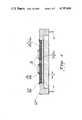
- FIG. 1is a cross-sectional schematic view illustrating a multilayer interconnect device using step coverage techniques common in the prior art
- FIG. 2is a cross-sectional schematic view illustrating the subject invention in an intermediate phase of fabrication
- FIG. 3is a cross-sectional schematic view illustrating a thin-film multilayer interconnect signal plane device fabricated using the subject invention having two signal planes;
- FIG. 4is a cross-sectional schematic view of a multichip thin-film module.
- each interconnect signal planerequires approximately ten (10) separate steps. These steps can be briefly described as follows:
- the substrate 14, FIG. 2is a standard silicon wafer in the preferred embodiment. Due to the particular materials used in the preferred embodiment, it is desirable to provide a diffussion barrier for the metal used in Step 2, discussed below. Other materials can be used as the substrate such as alumina, silicon carbide or other kinds of ceramic can also be used.
- the substrategoes through a standard cleaning procedure typically used for silicon wafers. The cleaning procedure includes a ten-minute immersion in a boiling solution of ammonium hydroxide, hydrogen peroxide and water. This is followed by a ten-minute rinse in flowing deionized water. After the wafer is rinsed, it is then immersed for ten minutes in a boiling solution of sulfuric acid and hydrogen peroxide.
- the second immersionis then followed by a second ten-minute rinse in flowing deionized water and then the wafer is spun dried in a nitrogen environment. It should be noted that other cleaning procedures can be used.
- the major objects of the cleaning stepare to provide a wafer free of particles and organic contaminants.
- the cleaned wafersare then loaded into planetary fixtures.
- a planetary fixtureis a device in which a plurality of wafers may be subjected to rotation about an axis to ensure uniform metallization as discussed below.
- three planetary fixtures, each containing seven wafers,may be inserted in an evaporator at a time.
- the wafersare then patterned using standard photolithographic techniques to form a first pattern 16, FIG. 2, of thin-film metallic interconnect lines on the surface of the substrate.
- the thickness of the thin-film metallic interconnect linesis in the range of 500 to 5,000 Angstroms.
- the thickness of the thin-film metallic interconnect linesis approximately 1,000 Angstroms consisting of approximately 100 Angstroms of chromium overlaid by 900 Angstroms of gold. These thin-film are sufficiently thin that planarization is easily accomplished. It should be noted that in other embodiments, other materials may be used to form the thin-film metallic pattern such as copper or silver.
- Another technique for providing the thin-film patternis in the use of the "lift off” technique.
- the waferis coated with a photoresist on which the thin-film pattern is defined.
- Metalis then evaporated onto the defined pattern and the photoresist is rinsed away, leaving the metal adhering in only the desired areas.
- a photosensitive polyimide precursor 18, FIG. 2is applied by spin coating on the patterned thin-film metallized substrate.
- other methods of applicationmay be used such as spraying, dipping and rolling.
- sprayingdipping and rolling.
- other materialsmay be used. These materials will be mentioned below and will not be discussed here since each particular material may require difference procedures than those discussed in the preferred embodiment.
- the product produced by Step 3is then prebaked at 70 degrees Centigrade for 180 minutes to remove the solvent and partially harden the polyimide precursor.
- the prebake timeis dependent on the thickness of the polyimide precursor.
- the thickness of the polyimide precursoris typically 11 microns in the preferred embodiment.
- the polyimide precursoris next exposed using relatively standard photolithographic techniques. First a photomask containing a pattern of the thin-film metallic interconnect lines is aligned with the thin-film metallic interconnect lines on the substrate. In the preferred embodiment, it is possible to see the thin-film metallic interconnect lines through the dielectric in order to accomplish the alignment process. After alignment, the polyimide precursor is then exposed to ultraviolet light to render the exposed areas insoluble.
- the exposed polyimide photoresistis then subjected to a fairly standard spray development technique.
- Other techniquesmay be used to develop the photoresist such as dipping techniques.
- the spray techniquethe wafer is placed on a spinner and then the developer is sprayed onto the spinning wafer. This technique is repeated until a series of trenches 20, FIG. 2, are formed over the thin-film metallic interconnect lines.
- the deviceis then placed into a plasma etcher to remove any dielectric residue remaining in the trenches over the thin-film metallic interconnect lines.
- a plasma etcherto remove any dielectric residue remaining in the trenches over the thin-film metallic interconnect lines.
- an eight percent oxygen/argon plasmais used at a pressure of 3 torr for 2 minutes at a power of 100 watts.
- the wafersare then subjected to an intermediate bake procedure to partially cure the dielectric.
- thisentails heating the wafers to 200 degrees Centigrade for 90 minutes.
- the purpose of the intermediate bakeis to prepare the device for the next step which is the electroplating step. If the dielectric layer is not sufficiently cured prior to electroplating, the dielectric may peel off during the electroplating stage.
- One of the effects of the intermediate bakeis to partially transform the polyimide precursor into polyimide.
- the thin-film metallic interconnect patternis next subjected to an electroplating procedure.
- This procedureincludes placing each wafer in a fixture in which electrical connection can be made to the thin-film metallic pattern.
- the wafer and fixtureare then placed in an electroplating bath and a series of thicker metallic interconnect lines 22, FIG. 2, are formed over the thin-film metallic interconnect pattern.
- the final thickness of the dielectric layeris chosen so that it is approximately equal to the thickness of the electroplated conductors.
- the thickness of the electroplated conductorsis approximately 5 microns.
- the thicker metal interconnect linesmay be in the range of 1 to 10 microns. It should also be noted that other techniques for forming the thicker metal interconnect lines may be used such as electroless plating.
- the product produced by Step 9is then subjected to a final bake to completely cure the polymer.
- the wafersare subjected to a post bake of 400 degrees Centigrade for 50 minutes in an inert atmosphere.
- the purpose of the post bakeis to fully convert the polyimide precursor to polyimide.
- One of the effects of the conversion of the precursor to polyimideis to cause the polymer to shrink in a predictable fashion.
- the polyimide dielectric layer and the thicker metal interconnect linesform a substantially planar surface.
- the process described abovemay be repeated to produce multilayered interconnect signal planes for connecting multiple integrated circuits as illustrated by device 24 in FIG. 3. It should be noted that before the procedures described above are repeated to produce each signal plane, an intermediate layer of dielectric 31 must be deposited for insulation purposes.
- the intermediate layercontains vias 26, FIG. 3, for electrical connection between selected interconnect lines.
- the interconnect lines 28 in the lower planeare in a direction generally orthogonal to the interconnect lines 30 in the upper plane.
- the intermediate dielectric layer and the metallic viasare produced in a fashion very similar to the production of the thicker metal interconnect lines. However, it is not necessary to produce a thin-film metallic base since the underlying metal conductors act as a base for the growth of metal in vias.
- a plurality of semiconductor integrated circuitsmay be electrically connected to the electrical interconnect planes of the subject invention.
- FIG. 4As can be seen in the figure, a silicon substrate 32 having thin-film multilayer interconnect signal planes 35 in accordance with the subject invention is electrically connected 34 to a plurality of semiconductor integrated circuits chips 36.
- a heat sink 38may be provided which is further described in U.S. patent application Ser. No. 698,472, filed Feb. 5, 1985 entitled A NEW MULTICHIP THIN-FILM MODULE.
- this pathis typically formed along a perimeter of the substrate so that the path can be subsequently destroyed after the thicker metallic interconnect lines have been formed. In other embodiments, this path may be located in other portions on the substrate. In those embodiments in which electroless plating is used to form the thicker metallic interconnect lines, this path is not necessary.
- a conventional polyimide precursormay be used instead of using a photosensitive polyimide precursor.
- a conventional polyimide precursoris used that is not photosensitive, different techniques must be used for creating patterns on the dielectric layer. Other techniques include masking the polyimide with an inorganic layer such as silicon dioxide or aluminum. These inorganic layers are patterned with conventional photolithography and serve as an etching mask for the polyimide. The etching procedure for the polyimide entails exposing the polyimide and mask structure to oxygen, or other plasma, which then removes the exposed areas which form the trenches discussed above.
- polymersmay be used instead of any form of polyimide.
- polymethylmethacrylate, or polytetrafluoroethyleneas the dielectric material.
- non-polymeric materialsfor example, silicon dioxide or silicon nitride may be used as the dielectric. If a non-polymeric material is used as the dielectric, a polymeric etching mask is typically applied and the above-discussed trenches are etched by liquid echants or plasma etching methods.
- the subject inventionis advantageous in that the characteristic impedance can be controlled to be within 30 to 300 ohms because the subject invention provides for well-defined geometrics which are highly planar.
- the precise geometric configuration of the conductive interconnect lines and their relationship to the dielectric layerscan be well controlled to produce interconnect lines which are substantially rectangular as opposed to trapezodial interconnect lines.
- the fact that the interconnect lines are substantially rectangular as opposed to trapezodicalis important, not so much from any specific shape requirements, but is important from the point of view that the specific dimensions (regardless of what dimensions or shape are chosen) are highly reproducible and uniform using the fabrication methods described herein.
- the actual device produced in accordance with the methods described hereinis closer to theoretical geometrics than devices using prior-art techniques.
- the impedance of the devicedepends on the dielectric constant and its geometrical dimensions which can both be fabricated to high precision with the planarized electrical connection process discussed in this patent application.
- the planarized processis superior to other non-planar processes because firstly, all dimension of the device are better defined and secondly the planar process is inherently less susceptible to defects (either a short between the different metal layers, or an open within a metal layer). It is a practical way to make multi-metal layer with thin dielectric insulator layers in between the metal layer.
Landscapes
- Engineering & Computer Science (AREA)
- Microelectronics & Electronic Packaging (AREA)
- Manufacturing & Machinery (AREA)
- Physics & Mathematics (AREA)
- Condensed Matter Physics & Semiconductors (AREA)
- General Physics & Mathematics (AREA)
- Computer Hardware Design (AREA)
- Power Engineering (AREA)
- Ceramic Engineering (AREA)
- Internal Circuitry In Semiconductor Integrated Circuit Devices (AREA)
- Design And Manufacture Of Integrated Circuits (AREA)
- Wire Bonding (AREA)
Abstract
Description
Claims (16)
Priority Applications (6)
| Application Number | Priority Date | Filing Date | Title |
|---|---|---|---|
| US06/697,092US4705606A (en) | 1985-01-31 | 1985-01-31 | Thin-film electrical connections for integrated circuits |
| EP85308479AEP0190490B1 (en) | 1985-01-31 | 1985-11-21 | Thin-film electrical connections for integrated circuits |
| DE8585308479TDE3576611D1 (en) | 1985-01-31 | 1985-11-21 | ELECTRICAL THICK LAYER CONNECTIONS FOR INTEGRATED CIRCUITS. |
| AT85308479TATE51109T1 (en) | 1985-01-31 | 1985-11-21 | ELECTRICAL THIN FILM CONNECTIONS FOR INTEGRATED CIRCUITS. |
| JP61016967AJPS61182245A (en) | 1985-01-31 | 1986-01-30 | Method and element for forming thin film-like mutual connection signal surface to connect a plurality of semiconductor ics |
| US07/257,171US4996584A (en) | 1985-01-31 | 1988-10-13 | Thin-film electrical connections for integrated circuits |
Applications Claiming Priority (1)
| Application Number | Priority Date | Filing Date | Title |
|---|---|---|---|
| US06/697,092US4705606A (en) | 1985-01-31 | 1985-01-31 | Thin-film electrical connections for integrated circuits |
Related Child Applications (1)
| Application Number | Title | Priority Date | Filing Date |
|---|---|---|---|
| US06891079Division | 1986-07-31 |
Publications (1)
| Publication Number | Publication Date |
|---|---|
| US4705606Atrue US4705606A (en) | 1987-11-10 |
Family
ID=24799756
Family Applications (1)
| Application Number | Title | Priority Date | Filing Date |
|---|---|---|---|
| US06/697,092Expired - LifetimeUS4705606A (en) | 1985-01-31 | 1985-01-31 | Thin-film electrical connections for integrated circuits |
Country Status (5)
| Country | Link |
|---|---|
| US (1) | US4705606A (en) |
| EP (1) | EP0190490B1 (en) |
| JP (1) | JPS61182245A (en) |
| AT (1) | ATE51109T1 (en) |
| DE (1) | DE3576611D1 (en) |
Cited By (16)
| Publication number | Priority date | Publication date | Assignee | Title |
|---|---|---|---|---|
| US4980034A (en)* | 1989-04-04 | 1990-12-25 | Massachusetts Institute Of Technology | High-density, multi-level interconnects, flex circuits, and tape for TAB |
| US5086500A (en)* | 1987-08-07 | 1992-02-04 | Tektronix, Inc. | Synchronized system by adjusting independently clock signals arriving at a plurality of integrated circuits |
| US5098860A (en)* | 1990-05-07 | 1992-03-24 | The Boeing Company | Method of fabricating high-density interconnect structures having tantalum/tantalum oxide layers |
| US5106461A (en)* | 1989-04-04 | 1992-04-21 | Massachusetts Institute Of Technology | High-density, multi-level interconnects, flex circuits, and tape for tab |
| US5220487A (en)* | 1992-01-27 | 1993-06-15 | International Business Machines Corporation | Electronic package with enhanced heat sinking |
| US5237268A (en)* | 1990-08-13 | 1993-08-17 | Kabushiki Kaisha Toshiba | Film carrier structure capable of simplifying test |
| US5305186A (en)* | 1993-01-27 | 1994-04-19 | International Business Machines Corporation | Power carrier with selective thermal performance |
| US5309025A (en)* | 1992-07-27 | 1994-05-03 | Sgs-Thomson Microelectronics, Inc. | Semiconductor bond pad structure and method |
| US5317194A (en)* | 1989-10-17 | 1994-05-31 | Kabushiki Kaisha Toshiba | Resin-sealed semiconductor device having intermediate silicon thermal dissipation means and embedded heat sink |
| US5391914A (en)* | 1994-03-16 | 1995-02-21 | The United States Of America As Represented By The Secretary Of The Navy | Diamond multilayer multichip module substrate |
| US5591676A (en)* | 1991-10-21 | 1997-01-07 | Motorola, Inc. | Method of making a semiconductor device having a low permittivity dielectric |
| US5986340A (en)* | 1996-05-02 | 1999-11-16 | National Semiconductor Corporation | Ball grid array package with enhanced thermal and electrical characteristics and electronic device incorporating same |
| US6034425A (en)* | 1999-03-17 | 2000-03-07 | Chipmos Technologies Inc. | Flat multiple-chip module micro ball grid array packaging |
| US6127099A (en)* | 1995-04-24 | 2000-10-03 | Nec Corporation | Method of producing a semiconductor device |
| WO2001031092A3 (en)* | 1999-10-28 | 2001-09-13 | Semitool Inc | Method, chemistry, and apparatus for noble metal electroplating a on a microelectronic workpiece |
| US20080050925A1 (en)* | 2006-08-24 | 2008-02-28 | Micron Technology, Inc. | Photoresist processing methods |
Families Citing this family (8)
| Publication number | Priority date | Publication date | Assignee | Title |
|---|---|---|---|---|
| DE3627417A1 (en)* | 1986-08-13 | 1988-02-18 | Siemens Ag | Process for producing low-resistance connections in the insulating layer between two metallisation levels |
| EP0286854A1 (en)* | 1987-04-13 | 1988-10-19 | Oerlikon-Contraves AG | Method for making a multilayer thin-film circuit |
| EP0372108B1 (en)* | 1988-12-05 | 1994-08-31 | Heinz Karl Diedrich | Vacuum container for cryogenically cooled electron device packaging |
| US5182420A (en)* | 1989-04-25 | 1993-01-26 | Cray Research, Inc. | Method of fabricating metallized chip carriers from wafer-shaped substrates |
| US5266446A (en)* | 1990-11-15 | 1993-11-30 | International Business Machines Corporation | Method of making a multilayer thin film structure |
| JPH0746755B2 (en)* | 1990-11-15 | 1995-05-17 | インターナシヨナル・ビジネス・マシーンズ・コーポレーシヨン | Method for manufacturing multilayer thin film structure |
| US5196377A (en)* | 1990-12-20 | 1993-03-23 | Cray Research, Inc. | Method of fabricating silicon-based carriers |
| EP0690494B1 (en) | 1994-06-27 | 2004-03-17 | Infineon Technologies AG | Connection and build-up-process for multi-chip-modules |
Citations (5)
| Publication number | Priority date | Publication date | Assignee | Title |
|---|---|---|---|---|
| US4134125A (en)* | 1977-07-20 | 1979-01-09 | Bell Telephone Laboratories, Incorporated | Passivation of metallized semiconductor substrates |
| US4210885A (en)* | 1978-06-30 | 1980-07-01 | International Business Machines Corporation | Thin film lossy line for preventing reflections in microcircuit chip package interconnections |
| US4254445A (en)* | 1979-05-07 | 1981-03-03 | International Business Machines Corporation | Discretionary fly wire chip interconnection |
| US4349862A (en)* | 1980-08-11 | 1982-09-14 | International Business Machines Corporation | Capacitive chip carrier and multilayer ceramic capacitors |
| US4430690A (en)* | 1982-10-07 | 1984-02-07 | International Business Machines Corporation | Low inductance MLC capacitor with metal impregnation and solder bar contact |
Family Cites Families (9)
| Publication number | Priority date | Publication date | Assignee | Title |
|---|---|---|---|---|
| FR2042059A5 (en)* | 1969-04-02 | 1971-02-05 | Ibm | |
| US3876460A (en)* | 1974-01-24 | 1975-04-08 | Plessey Inc | Fine-line thick-film substrate fabrication |
| JPS5571042A (en)* | 1978-11-09 | 1980-05-28 | Maruman Integrated Circuits | Semiconductor package and method of manufacturing same |
| US4221047A (en)* | 1979-03-23 | 1980-09-09 | International Business Machines Corporation | Multilayered glass-ceramic substrate for mounting of semiconductor device |
| US4367119A (en)* | 1980-08-18 | 1983-01-04 | International Business Machines Corporation | Planar multi-level metal process with built-in etch stop |
| US4336320A (en)* | 1981-03-12 | 1982-06-22 | Honeywell Inc. | Process for dielectric stenciled microcircuits |
| JPS57170524A (en)* | 1981-04-15 | 1982-10-20 | Toshiba Corp | Manufacture of semiconductor device |
| JPS57177537A (en)* | 1981-04-24 | 1982-11-01 | Matsushita Electric Ind Co Ltd | Isolation of semiconductor element |
| US4386116A (en)* | 1981-12-24 | 1983-05-31 | International Business Machines Corporation | Process for making multilayer integrated circuit substrate |
- 1985
- 1985-01-31USUS06/697,092patent/US4705606A/ennot_activeExpired - Lifetime
- 1985-11-21EPEP85308479Apatent/EP0190490B1/ennot_activeExpired - Lifetime
- 1985-11-21ATAT85308479Tpatent/ATE51109T1/ennot_activeIP Right Cessation
- 1985-11-21DEDE8585308479Tpatent/DE3576611D1/ennot_activeExpired - Lifetime
- 1986
- 1986-01-30JPJP61016967Apatent/JPS61182245A/enactivePending
Patent Citations (5)
| Publication number | Priority date | Publication date | Assignee | Title |
|---|---|---|---|---|
| US4134125A (en)* | 1977-07-20 | 1979-01-09 | Bell Telephone Laboratories, Incorporated | Passivation of metallized semiconductor substrates |
| US4210885A (en)* | 1978-06-30 | 1980-07-01 | International Business Machines Corporation | Thin film lossy line for preventing reflections in microcircuit chip package interconnections |
| US4254445A (en)* | 1979-05-07 | 1981-03-03 | International Business Machines Corporation | Discretionary fly wire chip interconnection |
| US4349862A (en)* | 1980-08-11 | 1982-09-14 | International Business Machines Corporation | Capacitive chip carrier and multilayer ceramic capacitors |
| US4430690A (en)* | 1982-10-07 | 1984-02-07 | International Business Machines Corporation | Low inductance MLC capacitor with metal impregnation and solder bar contact |
Non-Patent Citations (8)
| Title |
|---|
| Davidson, "Electrical Design of a High Speed Computer Packaging System", IEEE Transactions on Components, Hybrids, and Manufacturing Tech., CHMT-6, #3, (1983), 272-282. |
| Davidson, Electrical Design of a High Speed Computer Packaging System , IEEE Transactions on Components, Hybrids, and Manufacturing Tech., CHMT 6, 3, (1983), 272 282.* |
| Lewis, "High-Density High-Impedance Hybrid Circuits . . .", IEEE Transactions on Components, Hybrids, and Mfg. Tech., CHMT-2, #4, (1979), 441-450. |
| Lewis, High Density High Impedance Hybrid Circuits . . . , IEEE Transactions on Components, Hybrids, and Mfg. Tech., CHMT 2, 4, (1979), 441 450.* |
| Moriya et al, "A Planar Metallization Process . . .", International Electron Devices Meeting 1983 IEEE, (1983), 550-552. |
| Moriya et al, A Planar Metallization Process . . . , International Electron Devices Meeting 1983 IEEE, (1983), 550 552.* |
| Moriya et al., "High-Density Multilayer Interconnection with Photo-Sensitive . . .", 1984 Proceedings of the 34th Elec. Components Conf., (1984), 82-87. |
| Moriya et al., High Density Multilayer Interconnection with Photo Sensitive . . . , 1984 Proceedings of the 34 th Elec. Components Conf., (1984), 82 87.* |
Cited By (24)
| Publication number | Priority date | Publication date | Assignee | Title |
|---|---|---|---|---|
| US5086500A (en)* | 1987-08-07 | 1992-02-04 | Tektronix, Inc. | Synchronized system by adjusting independently clock signals arriving at a plurality of integrated circuits |
| US5106461A (en)* | 1989-04-04 | 1992-04-21 | Massachusetts Institute Of Technology | High-density, multi-level interconnects, flex circuits, and tape for tab |
| US4980034A (en)* | 1989-04-04 | 1990-12-25 | Massachusetts Institute Of Technology | High-density, multi-level interconnects, flex circuits, and tape for TAB |
| US5317194A (en)* | 1989-10-17 | 1994-05-31 | Kabushiki Kaisha Toshiba | Resin-sealed semiconductor device having intermediate silicon thermal dissipation means and embedded heat sink |
| US5436504A (en)* | 1990-05-07 | 1995-07-25 | The Boeing Company | Interconnect structures having tantalum/tantalum oxide layers |
| US5098860A (en)* | 1990-05-07 | 1992-03-24 | The Boeing Company | Method of fabricating high-density interconnect structures having tantalum/tantalum oxide layers |
| US5237268A (en)* | 1990-08-13 | 1993-08-17 | Kabushiki Kaisha Toshiba | Film carrier structure capable of simplifying test |
| US5396185A (en)* | 1990-08-13 | 1995-03-07 | Kabushiki Kaisha Toshiba | System and carrier for testing semiconductor integrated circuit devices |
| US5591676A (en)* | 1991-10-21 | 1997-01-07 | Motorola, Inc. | Method of making a semiconductor device having a low permittivity dielectric |
| US5220487A (en)* | 1992-01-27 | 1993-06-15 | International Business Machines Corporation | Electronic package with enhanced heat sinking |
| US5309025A (en)* | 1992-07-27 | 1994-05-03 | Sgs-Thomson Microelectronics, Inc. | Semiconductor bond pad structure and method |
| US5305186A (en)* | 1993-01-27 | 1994-04-19 | International Business Machines Corporation | Power carrier with selective thermal performance |
| US5391914A (en)* | 1994-03-16 | 1995-02-21 | The United States Of America As Represented By The Secretary Of The Navy | Diamond multilayer multichip module substrate |
| US6127099A (en)* | 1995-04-24 | 2000-10-03 | Nec Corporation | Method of producing a semiconductor device |
| US5986340A (en)* | 1996-05-02 | 1999-11-16 | National Semiconductor Corporation | Ball grid array package with enhanced thermal and electrical characteristics and electronic device incorporating same |
| US6034425A (en)* | 1999-03-17 | 2000-03-07 | Chipmos Technologies Inc. | Flat multiple-chip module micro ball grid array packaging |
| WO2001031092A3 (en)* | 1999-10-28 | 2001-09-13 | Semitool Inc | Method, chemistry, and apparatus for noble metal electroplating a on a microelectronic workpiece |
| US20040055895A1 (en)* | 1999-10-28 | 2004-03-25 | Semitool, Inc. | Platinum alloy using electrochemical deposition |
| US7300562B2 (en) | 1999-10-28 | 2007-11-27 | Semitool, Inc. | Platinum alloy using electrochemical deposition |
| US20080050925A1 (en)* | 2006-08-24 | 2008-02-28 | Micron Technology, Inc. | Photoresist processing methods |
| US20110159698A2 (en)* | 2006-08-24 | 2011-06-30 | Micron Technology, Inc. | Photoresist Processing Methods |
| US7977037B2 (en)* | 2006-08-24 | 2011-07-12 | Micron Technology, Inc. | Photoresist processing methods |
| US8283112B2 (en) | 2006-08-24 | 2012-10-09 | Micron Technology, Inc. | Photoresist processing methods |
| US8685625B2 (en) | 2006-08-24 | 2014-04-01 | Micron Technology, Inc. | Photoresist processing methods |
Also Published As
| Publication number | Publication date |
|---|---|
| DE3576611D1 (en) | 1990-04-19 |
| ATE51109T1 (en) | 1990-03-15 |
| JPS61182245A (en) | 1986-08-14 |
| EP0190490A2 (en) | 1986-08-13 |
| EP0190490A3 (en) | 1987-01-28 |
| EP0190490B1 (en) | 1990-03-14 |
Similar Documents
| Publication | Publication Date | Title |
|---|---|---|
| US4996584A (en) | Thin-film electrical connections for integrated circuits | |
| US4705606A (en) | Thin-film electrical connections for integrated circuits | |
| US4770897A (en) | Multilayer interconnection system for multichip high performance semiconductor packaging | |
| EP0099544B1 (en) | Method for forming conductive lines and via studs on lsi carrier substrates | |
| Jensen et al. | Copper/polyimide materials system for high performance packaging | |
| US4920639A (en) | Method of making a multilevel electrical airbridge interconnect | |
| US4367119A (en) | Planar multi-level metal process with built-in etch stop | |
| US5436504A (en) | Interconnect structures having tantalum/tantalum oxide layers | |
| US5106461A (en) | High-density, multi-level interconnects, flex circuits, and tape for tab | |
| EP0411165B1 (en) | Method of forming of an integrated circuit chip packaging structure | |
| US4980034A (en) | High-density, multi-level interconnects, flex circuits, and tape for TAB | |
| US4918811A (en) | Multichip integrated circuit packaging method | |
| KR960013632B1 (en) | Multichip integrated circuit package configuration and method | |
| US5112448A (en) | Self-aligned process for fabrication of interconnect structures in semiconductor applications | |
| EP0450381B1 (en) | Multilayer interconnection structure | |
| US4447824A (en) | Planar multi-level metal process with built-in etch stop | |
| US4536249A (en) | Integrated circuit processing methods | |
| US4520554A (en) | Method of making a multi-level metallization structure for semiconductor device | |
| US5661341A (en) | Method of manufacturing a composite structure for use in electronic devices and structure, manufactured by said method | |
| JPH088302B2 (en) | Interconnect in multilayer wiring and method of forming the same | |
| McDonald et al. | Multilevel interconnections for wafer scale integration | |
| EP1465246B1 (en) | Method for producing electrical through hole interconnects | |
| JP3272945B2 (en) | Manufacturing method of wiring board | |
| Ray et al. | Dual-level metal (DLM) method for fabricating thin film wiring structures | |
| JPH0569308B2 (en) |
Legal Events
| Date | Code | Title | Description |
|---|---|---|---|
| AS | Assignment | Owner name:GOULD INC., A CORP OF DE Free format text:ASSIGNMENT OF ASSIGNORS INTEREST.;ASSIGNORS:YOUNG, PETER L.;CECH, JAY;LI, KIN;REEL/FRAME:004365/0405 Effective date:19850129 | |
| STCF | Information on status: patent grant | Free format text:PATENTED CASE | |
| FEPP | Fee payment procedure | Free format text:PAYOR NUMBER ASSIGNED (ORIGINAL EVENT CODE: ASPN); ENTITY STATUS OF PATENT OWNER: LARGE ENTITY | |
| FEPP | Fee payment procedure | Free format text:PAYER NUMBER DE-ASSIGNED (ORIGINAL EVENT CODE: RMPN); ENTITY STATUS OF PATENT OWNER: LARGE ENTITY Free format text:PAYOR NUMBER ASSIGNED (ORIGINAL EVENT CODE: ASPN); ENTITY STATUS OF PATENT OWNER: LARGE ENTITY | |
| FPAY | Fee payment | Year of fee payment:4 | |
| FPAY | Fee payment | Year of fee payment:8 | |
| FPAY | Fee payment | Year of fee payment:12 | |
| AS | Assignment | Owner name:AMERICAN MICROSYSTEMS, INC., IDAHO Free format text:ASSIGNMENT OF ASSIGNORS INTEREST;ASSIGNOR:GOULD INC.;REEL/FRAME:011284/0696 Effective date:20000724 | |
| AS | Assignment | Owner name:AMERICAN MICROSYSTEMS HOLDING CORPORATION, IDAHO Free format text:MERGER;ASSIGNOR:AMERICAN MICROSYSTEMS, INC.;REEL/FRAME:011277/0491 Effective date:19970725 Owner name:GA-TEK INC., OHIO Free format text:MERGER AND CHANGE OF NAME;ASSIGNOR:AMERICAN MICROSYSTEMS HOLDING CORPORATION;REEL/FRAME:011277/0509 Effective date:19980101 | |
| AS | Assignment | Owner name:AMI SPINCO, INC., IDAHO Free format text:ASSIGNMENT OF ASSIGNORS INTEREST;ASSIGNOR:GA-TEK, INC.;REEL/FRAME:011369/0264 Effective date:20000729 | |
| AS | Assignment | Owner name:CREDIT SUISSE FIRST BOSTON, AS COLLATERAL AGENT, N Free format text:SECURITY INTEREST;ASSIGNOR:AMI SPINCO, INC.;REEL/FRAME:011457/0562 Effective date:20001221 | |
| AS | Assignment | Owner name:AMI SEMICONDUCTOR, INC., IDAHO Free format text:MERGER/CHANGE OF NAME;ASSIGNOR:AMI SPINCO, INC.;REEL/FRAME:011601/0413 Effective date:20001221 | |
| AS | Assignment | Owner name:AMI SPINCO, INC., IDAHO Free format text:RELEASE BY SECURED PARTY;ASSIGNOR:CREDIT SUISSE AG, CAYMAN ISLANDS BRANCH (F/K/A CREDIT SUISSE FIRST BOSTON);REEL/FRAME:038355/0131 Effective date:20160401 Owner name:AMI SEMICONDUCTOR, INC., IDAHO Free format text:RELEASE BY SECURED PARTY;ASSIGNOR:CREDIT SUISSE AG, CAYMAN ISLANDS BRANCH (F/K/A CREDIT SUISSE FIRST BOSTON);REEL/FRAME:038355/0131 Effective date:20160401 |